Embed Size (px)
Citation preview
ARTICLES
Additive nanomanufacturing – A review
D.S. Engstrom, B. Porter, M. Pacios, and H. Bhaskarana)
Department of Materials, University of Oxford, Oxford OX1 3PH, United Kingdom
(Received 8 April 2014; accepted 10 June 2014)
Additive manufacturing has provided a pathway for inexpensive and flexible manufacturing ofspecialized components and one-off parts. At the nanoscale, such techniques are less ubiquitous.Manufacturing at the nanoscale is dominated by lithography tools that are too expensive forsmall- and medium-sized enterprises (SMEs) to invest in. Additive nanomanufacturing (ANM)empowers smaller facilities to design, create, and manufacture on their own while providinga wider material selection and flexible design. This is especially important as nanomanufacturingthus far is largely constrained to 2-dimensional patterning techniques and being able tomanufacture in 3-dimensions could open up new concepts. In this review, we outline the state-of-the-art within ANM technologies such as electrohydrodynamic jet printing, dip-pen lithography,direct laser writing, and several single particle placement methods such as optical tweezers andelectrokinetic nanomanipulation. The ANM technologies are compared in terms of depositionspeed, resolution, and material selection and finally the future prospects of ANM are discussed.This review is up-to-date until April 2014.
I. INTRODUCTION
Nanoscale manufacturing techniques are essential to liveup to the promises made on the prospects of nanotechnol-ogy; without methods to rapidly fabricate and test newconcepts, innovation in this emerging field can be stifled.Additive manufacturing is already used at the macroscalefor rapid prototyping and low volume production in areassuch as dental and medical care, automotive, aerospace,fashion, and entertainment.1 These areas have benefitedfrom the freedom of design and reduced time-to-marketprovided by additive manufacturing. Unfortunately, suchrapid prototyping techniques are yet to be developed fornanomanufacturing. Such a technology would have thepotential to transform manufacturing on the nanoscale aswell. Within the scientific community, the focus has beenon tissue engineering,2,3 electronics,4,5 microfluidics,6,7
orthopedics,8,9 health care,10,11 and materials,12 but as theresolution improves more applications such as photovol-taics,13,14 optics,15 and nanoelectronics16,17 are emerging.
For decades, realistic options for full scale industrialnanomanufacturing have relied on photolithography usingelectromagnetic radiation with increasingly shorter wavelength.18 The equipment to reach nanometer dimensionsreliably is, however, prohibitively expensive, therebyexcluding smaller R&D facilities and small and mediumenterprises (SMEs) from taking advantage of their innova-tions. Electron beam lithography (EBL) offers flexibilityand high resolution19 for R&D and is comparably cheap but
is still only affordable for well-funded universities andcompanies with large capital investments. Device fabrica-tion using both photolithography and EBL relies onexposures of multiple layers of polymer thin films. Theseare planar technologies operating virtually only in twodimensions; developing fabrication methods that extendinto the third dimension seems an obvious way to savespace, cost and to gain additional functionality. Moreover,the lift-off and etching processes related to resist-basedmanufacturing are extremely wasteful as only a smallpercentage of the used materials is turned into functionalelements.20 Additive nanomanufacturing (ANM) does notseek to replace the resist-based planar manufacturingmethods used for integrated circuit (IC) fabrication, butrather seeks to add functionally in ways these technologiescannot. More importantly, it could change the way we thinkabout manufacturing at the nanoscale, which could also leadto much greater flexibility in the design.Before we begin a technical review, we will define
ANM as we perceive it for the purposes of this review.We define ANM as incorporating techniques that directlyadd the desired material in its final shape, with sub-100 nm resolution, without subtractive removal. Thisdefinition excludes thin film fabrication methods such asatomic layer deposition (ALD) and molecular beamepitaxy (MBE) although these methods might success-fully be combined with additive manufacturing methods.Direct laser writing (DLW), near-field optical lithogra-phy, and plasmonic lensing are borderline ANM tech-nologies, as these can produce structures in their finalshape after an additional development process. Forcompleteness these are included in the review.
a)Address all correspondence to this author.e-mail: [email protected]
DOI: 10.1557/jmr.2014.159
J. Mater. Res., 2014 �Materials Research Society 2014 1
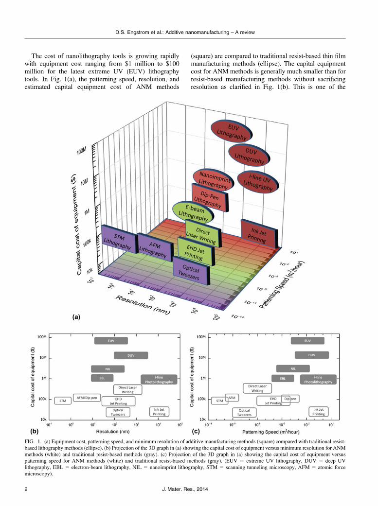
The cost of nanolithography tools is growing rapidlywith equipment cost ranging from $1 million to $100million for the latest extreme UV (EUV) lithographytools. In Fig. 1(a), the patterning speed, resolution, andestimated capital equipment cost of ANM methods
(square) are compared to traditional resist-based thin filmmanufacturing methods (ellipse). The capital equipmentcost for ANM methods is generally much smaller than forresist-based manufacturing methods without sacrificingresolution as clarified in Fig. 1(b). This is one of the
FIG. 1. (a) Equipment cost, patterning speed, and minimum resolution of additive manufacturing methods (square) compared with traditional resist-based lithography methods (ellipse). (b) Projection of the 3D graph in (a) showing the capital cost of equipment versus minimum resolution for ANMmethods (white) and traditional resist-based methods (gray). (c) Projection of the 3D graph in (a) showing the capital cost of equipment versuspatterning speed for ANM methods (white) and traditional resist-based methods (gray). (EUV 5 extreme UV lithography, DUV 5 deep UVlithography, EBL 5 electron-beam lithography, NIL 5 nanoimprint lithography, STM 5 scanning tunneling microscopy, AFM 5 atomic forcemicroscopy).
D.S. Engstrom et al.: Additive nanomanufacturing – A review
J. Mater. Res., 20142
primary reasons ANM is envisioned to spread to SMEsand research labs. The price per unit can still be high foradditive manufacturing1 because of the relatively lowpatterning speed as shown in Fig. 1(c); but for low volumeand high value products, the comparatively low invest-ment prospects of this technique can be particularlyattractive.
When comparing manufacturing methods at the micro-and nanoscale, one often focuses on the resolution of thetechnology as it is closely linked to the performance ofthe product. For commercial use, resolution is, however,only one significant parameter as the ability to positionstructures relative to one another (accuracy/alignment),writing speed and materials are equally important.
Manufacturing at the nanoscale is very different frommacroscale manufacturing because of fundamental phys-ical limits. Therefore, the difficulties met are also verydifferent. Fabrication at the nanoscale is a matter ofmanipulating very few atoms or molecules at a time andmanufacturing variations of just a single atom or mole-cule can lead to device failure. Additionally, structureswith dimensions below 50 nm also have a reducedmelting point which can affect their mechanical stabil-ity21,22 and even defining alloy composition, doping levelsand crystallinity becomes complex as the presence orspatial location of a single atom will change the materialproperties. At the nanoscale, gravity is insignificant andthe dominating forces are the surface interactions such asvan derWaals forces that can cause unwanted adhesion. Inliquid, Brownian motion and convection forces are com-paratively strong making particle capture difficult. Even inair or vacuum, vibrations from fans, pumps or passingtraffic can render structural alignment impossible.
For ANM, the challenge is to manufacture nanoscalestructures at a large scale with great accuracy, highresolution, low cost and using materials ranging frombiomaterials to ceramics and metals. However, ANMdoes not aim to compete with existing technologies and itcan create new ways to manufacture and change theway we design products. In this review, we focus onthe range of ANM methods available today and thelevel they are at in terms of resolution, accuracy,speed, and materials. We have divided the manu-facturing methods into two groups: direct writing andsingle particle placement. Within each group, thestate-of-the-art ANM techniques will be describedand evaluated and finally these techniques will becompared to provide an outlook on ANM and itsprospects over the next decade.
II. DIRECT WRITING
Direct writing of nanoscale devices composed ofmetals, insulators, and organic materials is of interestfor a range of ANM applications. Here, we review recent
advances in three key direct writing methods of nano-structures: dip-pen nanolithography (DPN), electrohy-drodynamic (EHD) jet printing, and DLW. All threetechnologies are able to achieve sub-30 nm resolution,relatively high writing speed, and the capacity for3-dimensional nanomanufacturing. The choice of mate-rials, at least for DPN and EHD jet printing, is alreadyvast ranging from metals to biomaterials while thematerial selection for DLW is also increasing. In thissection, the promising future of direct writing ANM isoutlined through examples of the state-of-the-art foreach of these three technologies.
A. Dip-pen nanolithography
DPN is a scanning probe microscopy (SPM)-basedflexible nanofabrication process for making 2D nanoscalefeatures that uniquely combines direct-write soft-mattercompatibility with the high resolution and registry of atomicforce microscopy (AFM), all in a mask-free and biocom-patible system.23 Originally, scanning probe microscopes(SPMs), such as the scanning tunnelingmicroscope (STM)24
and the atomic force microscope (AFM),25 emerged asnanoscale imaging and spectroscopic tools in the mid1980s. Soon thereafter manipulation of single-atoms26 andatom-by-atom construction of nanopatterns marked the birthof scanning probe lithography (SPL), suggesting that SPMscould indeed be used for molecular printing or perhaps evenmanufacturing.27
Hereafter, a series of indirect SPL methods based ondestructive delivery of energy to create functionalpatterns were developed. Taking advantage of thepositioning resolution enabled by piezo-actuation andthe nanoscale radii of the tips, scientists were able togenerate sub-50-nm features by scratching, etching, andoxidizing surfaces.28 A process known as nanoshavingor nanografting uses the tip of an AFM and an appliedforce to remove a molecular monolayer on gold in a site-specific fashion29 and anodic oxidation of silicon wasdeveloped by Quate and colleagues for patterning siliconsubstrates.30,31
In contrast to nanoshaving and nanografting, DPNselectively transfers material from an ink-coated probe tipon to a surface with a variety of ink-surface combina-tions.23,32 A schematic of the process is shown in Fig. 2.Ink molecules are transported via mass diffusion from thetip on to the surface. Features are formed on the surface viaeither chemisorption based self-assembly or physisorp-tion.35 Ink transport is mediated by the presence of thewater meniscus that forms when the tip is brought in closeproximity to the surface under ambient conditions. Due tothe naturally occurring water meniscus for mass transferthis method also avoids the necessity for ultrahighvacuum. Moreover, there is no need to expose the sub-strate to ultraviolet, ion- or electron-beam radiation,
D.S. Engstrom et al.: Additive nanomanufacturing – A review
3J. Mater. Res., 2014

characteristic of indirect patterning techniques, and there-fore DPN can be used to print fragile or reactive organicand biological materials.
From initial demonstrations involving alkanethiols ongold,36 DPN has evolved into a versatile technique used towrite or template both inorganic and organic nanostruc-tures.23,32 Polymers,37 colloidal nanoparticles (e.g., mag-netic nanocrystals and carbon nanotubes (CNTs)),38–40
electrodeposited metals,41 sol-gel precursors,42 smallorganic molecules,43,44 biomolecules (proteins45,46 andoligonucleotides47) and even single viruses48 and bacteriahave been patterned on a variety of substrates (includingmetals, semiconductors, and insulators)38 by controllingvarious experimental parameters such as ambient humid-ity, writing speed, and dwell time.44,49 In fact, theseexperimental parameters serve a useful function of beingthe levers that control the features size. However, DPNinitially faced a drawback common to other indirect SPL ofpoor throughput. This was because the first incarnations ofDPN were serial processes, and were thus lower inthroughput than stamping or optical lithography-basedtechniques. To compete with these techniques, it wasnecessary to increase the throughput of DPN by parallelizing
the deposition process. The scalability of DPN wasdemonstrated by Salaita et al.50 who were able tofabricate a 55,000-pen 2D array generating 88 millionAu dots (pitch distance 400 nm) with a diameterequal to 100 6 20 nm (see Fig. 3). This increased thethroughput of DPN by four orders of magnitude,fabricating the 88 million dots in approximately5 min. Even with impressive recent advances in can-tilever array design, such arrays tend to be highlyspecialized for a given application. They are alsomechanically fragile, expensive, and often difficult toimplement. It is therefore difficult to imagine commer-cially viable production methods based on scanningprobe systems that rely on conventional cantilevers.51
Hence new methods to reduce the cost barriers asso-ciated with massively parallel DPN were demonstratedto achieve high-throughput and to define patterns withhigh-resolution.52
The second key advance in molecular printing wastherefore to replace the cantilever with an elastomericpyramid on a solid backing. This approach is calledpolymer pen lithography (PPL) and is shown in Fig. 4.53
The elastomeric tips can print a digitized pattern with spot
FIG. 2. (a) Schematic representation of the basic molecular deposition by DPN through a water meniscus formed between the scanning probe tip andthe substrate surface. (b) Direct deposition of SAMs (16-mercaptohexadecanoic acid) on Ag as an etch resist to pattern 70-nm wide features.Reproduced from Refs. 33 and 34.
FIG. 3. (a) Optical micrograph of part of the 2D array of cantilevers used for patterning. Inset: SEM image of the cantilever arrays at a differentviewing angle. (b) Large-area SEM image of part of an 88,000 ,000-gold-dot array (40 � 40 within each block) on an oxidized silicon substrate.(c) Representative AFM topographical image of part of one of the blocks, where the dot-to-dot distance is 400 nm and the dot diameter is 1006 20 nm.Reproduced from Ref. 50.
D.S. Engstrom et al.: Additive nanomanufacturing – A review
J. Mater. Res., 20144
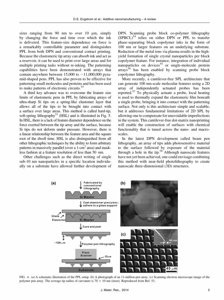
sizes ranging from 90 nm to over 10 lm, simplyby changing the force and time over which the inkis delivered. This feature-size dependence on force isa remarkably controllable parameter and distinguishesPPL from both DPN and conventional contact printing.Because the elastomeric tip array can absorb ink and act asa reservoir, it can be used to print over large areas and formultiple printing tasks without re-inking. The patterningcapabilities have been demonstrated with arrays thatcontain anywhere between 15,000 to ;11,000,000 pyra-mid-shaped pens. PPL has also proven to be effective forpatterning small molecules and proteins and has been usedto make patterns of electronic circuits.53
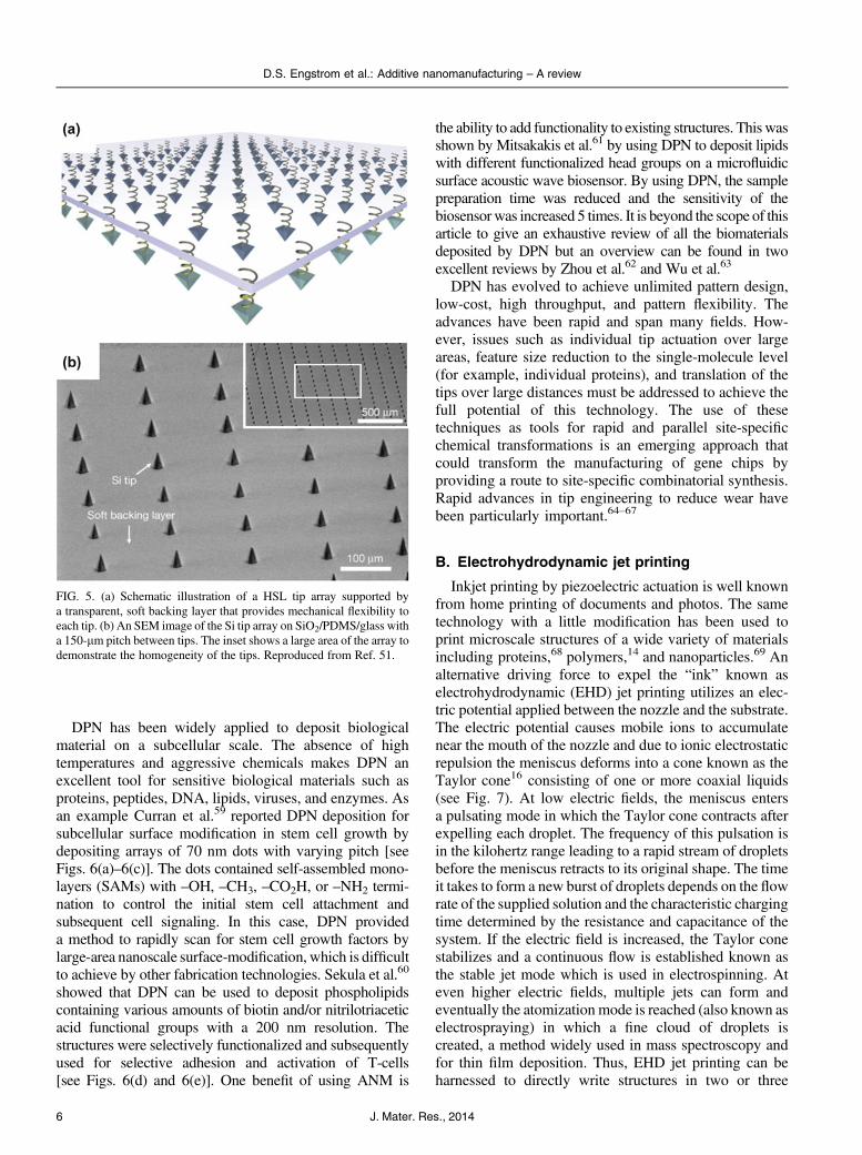
A third key advance was to overcome the feature sizelimits of elastomeric pens in PPL by fabricating arrays ofultra-sharp Si tips on a spring-like elastomer layer thatallows all of the tips to be brought into contact witha surface over large areas. This method is called hard-tip,soft-spring lithography51 (HSL) and is illustrated in Fig. 5.In HSL, there is a lack of feature diameter dependence on theforce exerted between the tip array and the surface, becauseSi tips do not deform under pressure. However, there isa linear relationship between the feature area and the squareroot of the dwell time. HSL is also distinguished from allother lithographic techniques by the ability to form arbitrarypatterns in massively parallel (over a 1-cm2 area) and mask-less fashion at a feature resolution of less than 50 nm.
Other challenges such as the direct writing of singlesub-10 nm nanoparticles in a specific location individu-ally on a substrate have allowed further development of
DPN. Scanning probe block co-polymer lithography(SPBCL)54 relies on either DPN or PPL to transferphase-separating block copolymer inks in the form of100 nm or larger features on an underlying substrate.Reduction of the metal ions via plasma results in the high-yield formation of single crystal nanoparticles per blockcopolymer feature. For instance, integration of individualnanoparticles on devices55 or single-molecule proteinarrays56 has been enabled by scanning probe blockcopolymer lithography.
More recently, a cantilever-free SPL architecture thatcan generate 100 nm-scale molecular features using a 2Darray of independently actuated probes has beenreported.57 To physically actuate a probe, local heatingis used to thermally expand the elastomeric film beneatha single probe, bringing it into contact with the patterningsurface. Not only is this architecture simple and scalable,but it addresses fundamental limitations of 2D SPL byallowing one to compensate for unavoidable imperfectionsin the system. This cantilever-free dot-matrix nanoprintingwill enable the construction of surfaces with chemicalfunctionality that is tuned across the nano- and macro-scales.
In the latest DPN development called beam penlithography, an array of tips adds photosensitive materialto the surface followed by exposure of the materialthrough a hole in the tip.58 Although nanoscale featureshave not yet been achieved, one could envisage combiningthis method with near-field photolithography to createnanoscale three-dimensional (3D) structures.
FIG. 4. (a) A schematic illustration of the PPL setup. (b) A photograph of an 11-million-pen array. (c) Scanning electron microscope image of thepolymer pen array. The average tip radius of curvature is 70 6 10 nm (inset). Reproduced from Ref. 53.
D.S. Engstrom et al.: Additive nanomanufacturing – A review
5J. Mater. Res., 2014
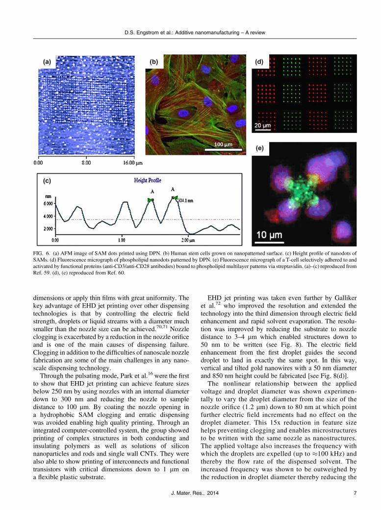
DPN has been widely applied to deposit biologicalmaterial on a subcellular scale. The absence of hightemperatures and aggressive chemicals makes DPN anexcellent tool for sensitive biological materials such asproteins, peptides, DNA, lipids, viruses, and enzymes. Asan example Curran et al.59 reported DPN deposition forsubcellular surface modification in stem cell growth bydepositing arrays of 70 nm dots with varying pitch [seeFigs. 6(a)–6(c)]. The dots contained self-assembled mono-layers (SAMs) with –OH, –CH3, –CO2H, or –NH2 termi-nation to control the initial stem cell attachment andsubsequent cell signaling. In this case, DPN provideda method to rapidly scan for stem cell growth factors bylarge-area nanoscale surface-modification, which is difficultto achieve by other fabrication technologies. Sekula et al.60
showed that DPN can be used to deposit phospholipidscontaining various amounts of biotin and/or nitrilotriaceticacid functional groups with a 200 nm resolution. Thestructures were selectively functionalized and subsequentlyused for selective adhesion and activation of T-cells[see Figs. 6(d) and 6(e)]. One benefit of using ANM is
the ability to add functionality to existing structures. This wasshown by Mitsakakis et al.61 by using DPN to deposit lipidswith different functionalized head groups on a microfluidicsurface acoustic wave biosensor. By using DPN, the samplepreparation time was reduced and the sensitivity of thebiosensorwas increased 5 times. It is beyond the scope of thisarticle to give an exhaustive review of all the biomaterialsdeposited by DPN but an overview can be found in twoexcellent reviews by Zhou et al.62 and Wu et al.63
DPN has evolved to achieve unlimited pattern design,low-cost, high throughput, and pattern flexibility. Theadvances have been rapid and span many fields. How-ever, issues such as individual tip actuation over largeareas, feature size reduction to the single-molecule level(for example, individual proteins), and translation of thetips over large distances must be addressed to achieve thefull potential of this technology. The use of thesetechniques as tools for rapid and parallel site-specificchemical transformations is an emerging approach thatcould transform the manufacturing of gene chips byproviding a route to site-specific combinatorial synthesis.Rapid advances in tip engineering to reduce wear havebeen particularly important.64–67
B. Electrohydrodynamic jet printing
Inkjet printing by piezoelectric actuation is well knownfrom home printing of documents and photos. The sametechnology with a little modification has been used toprint microscale structures of a wide variety of materialsincluding proteins,68 polymers,14 and nanoparticles.69 Analternative driving force to expel the “ink” known aselectrohydrodynamic (EHD) jet printing utilizes an elec-tric potential applied between the nozzle and the substrate.The electric potential causes mobile ions to accumulatenear the mouth of the nozzle and due to ionic electrostaticrepulsion the meniscus deforms into a cone known as theTaylor cone16 consisting of one or more coaxial liquids(see Fig. 7). At low electric fields, the meniscus entersa pulsating mode in which the Taylor cone contracts afterexpelling each droplet. The frequency of this pulsation isin the kilohertz range leading to a rapid stream of dropletsbefore the meniscus retracts to its original shape. The timeit takes to form a new burst of droplets depends on the flowrate of the supplied solution and the characteristic chargingtime determined by the resistance and capacitance of thesystem. If the electric field is increased, the Taylor conestabilizes and a continuous flow is established known asthe stable jet mode which is used in electrospinning. Ateven higher electric fields, multiple jets can form andeventually the atomization mode is reached (also known aselectrospraying) in which a fine cloud of droplets iscreated, a method widely used in mass spectroscopy andfor thin film deposition. Thus, EHD jet printing can beharnessed to directly write structures in two or three
FIG. 5. (a) Schematic illustration of a HSL tip array supported bya transparent, soft backing layer that provides mechanical flexibility toeach tip. (b) An SEM image of the Si tip array on SiO2/PDMS/glass witha 150-lm pitch between tips. The inset shows a large area of the array todemonstrate the homogeneity of the tips. Reproduced from Ref. 51.
D.S. Engstrom et al.: Additive nanomanufacturing – A review
J. Mater. Res., 20146
dimensions or apply thin films with great uniformity. Thekey advantage of EHD jet printing over other dispensingtechnologies is that by controlling the electric fieldstrength, droplets or liquid streams with a diameter muchsmaller than the nozzle size can be achieved.70,71 Nozzleclogging is exacerbated by a reduction in the nozzle orificeand is one of the main causes of dispensing failure.Clogging in addition to the difficulties of nanoscale nozzlefabrication are some of the main challenges in any nano-scale dispensing technology.
Through the pulsating mode, Park et al.16 were the firstto show that EHD jet printing can achieve feature sizesbelow 250 nm by using nozzles with an internal diameterdown to 300 nm and reducing the nozzle to sampledistance to 100 lm. By coating the nozzle opening ina hydrophobic SAM clogging and erratic dispensingwas avoided enabling high quality printing. Through anintegrated computer-controlled system, the group showedprinting of complex structures in both conducting andinsulating polymers as well as solutions of siliconnanoparticles and rods and single wall CNTs. They werealso able to show printing of interconnects and functionaltransistors with critical dimensions down to 1 lm ona flexible plastic substrate.
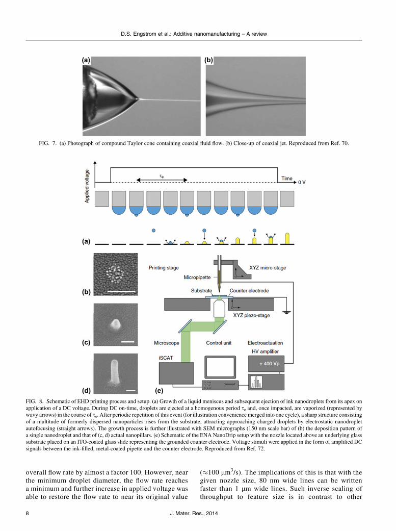
EHD jet printing was taken even further by Gallikeret al.72 who improved the resolution and extended thetechnology into the third dimension through electric fieldenhancement and rapid solvent evaporation. The resolu-tion was improved by reducing the substrate to nozzledistance to 3–4 lm which enabled structures down to50 nm to be written (see Fig. 8). The electric fieldenhancement from the first droplet guides the seconddroplet to land in exactly the same spot. In this way,vertical and tilted gold nanowires with a 50 nm diameterand 850 nm height could be fabricated [see Fig. 8(d)].
The nonlinear relationship between the appliedvoltage and droplet diameter was shown experimen-tally to vary the droplet diameter from the size of thenozzle orifice (1.2 lm) down to 80 nm at which pointfurther electric field increments had no effect on thedroplet diameter. This 15x reduction in feature sizehelps preventing clogging and enables microstructuresto be written with the same nozzle as nanostructures.The applied voltage also increases the frequency withwhich the droplets are expelled (up to �100 kHz) andthereby the flow rate of the dispensed solvent. Theincreased frequency was shown to be outweighed bythe reduction in droplet diameter thereby reducing the
FIG. 6. (a) AFM image of SAM dots printed using DPN. (b) Human stem cells grown on nanopatterned surface. (c) Height profile of nanodots ofSAMs. (d) Fluorescence micrograph of phospholipid nanodots patterned by DPN. (e) Fluorescence micrograph of a T-cell selectively adhered to andactivated by functional proteins (anti-CD3/anti-CD28 antibodies) bound to phospholipid multilayer patterns via streptavidin. (a)–(c) reproduced fromRef. 59. (d), (e) reproduced from Ref. 60.
D.S. Engstrom et al.: Additive nanomanufacturing – A review
7J. Mater. Res., 2014
overall flow rate by almost a factor 100. However, nearthe minimum droplet diameter, the flow rate reachesa minimum and further increase in applied voltage wasable to restore the flow rate to near its original value
(�100 lm3/s). The implications of this is that with thegiven nozzle size, 80 nm wide lines can be writtenfaster than 1 lm wide lines. Such inverse scaling ofthroughput to feature size is in contrast to other
FIG. 8. Schematic of EHD printing process and setup. (a) Growth of a liquid meniscus and subsequent ejection of ink nanodroplets from its apex onapplication of a DC voltage. During DC on-time, droplets are ejected at a homogenous period se and, once impacted, are vaporized (represented bywavy arrows) in the course of se. After periodic repetition of this event (for illustration convenience merged into one cycle), a sharp structure consistingof a multitude of formerly dispersed nanoparticles rises from the substrate, attracting approaching charged droplets by electrostatic nanodropletautofocusing (straight arrows). The growth process is further illustrated with SEM micrographs (150 nm scale bar) of (b) the deposition pattern ofa single nanodroplet and that of (c, d) actual nanopillars. (e) Schematic of the ENA NanoDrip setup with the nozzle located above an underlying glasssubstrate placed on an ITO-coated glass slide representing the grounded counter electrode. Voltage stimuli were applied in the form of amplified DCsignals between the ink-filled, metal-coated pipette and the counter electrode. Reproduced from Ref. 72.
FIG. 7. (a) Photograph of compound Taylor cone containing coaxial fluid flow. (b) Close-up of coaxial jet. Reproduced from Ref. 70.
D.S. Engstrom et al.: Additive nanomanufacturing – A review
J. Mater. Res., 20148
techniques and can thus be advantageous for nano-manufacturing.
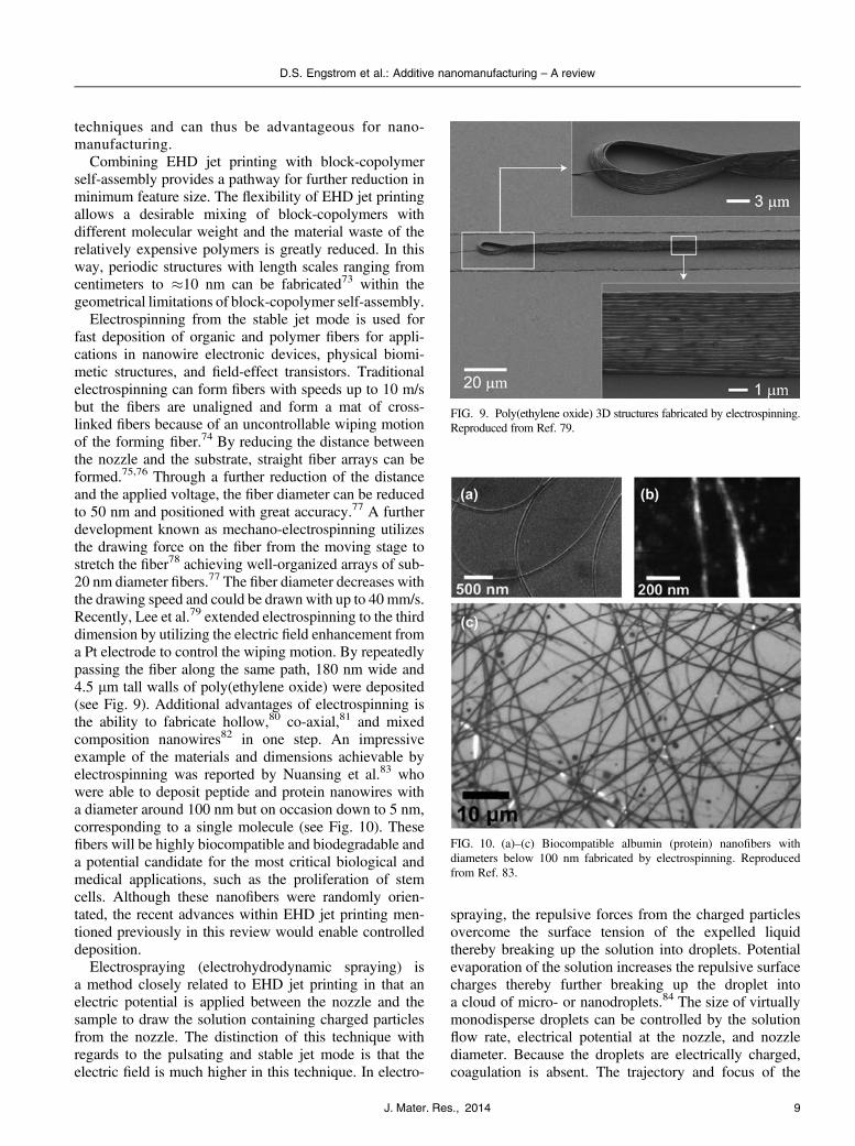
Combining EHD jet printing with block-copolymerself-assembly provides a pathway for further reduction inminimum feature size. The flexibility of EHD jet printingallows a desirable mixing of block-copolymers withdifferent molecular weight and the material waste of therelatively expensive polymers is greatly reduced. In thisway, periodic structures with length scales ranging fromcentimeters to �10 nm can be fabricated73 within thegeometrical limitations of block-copolymer self-assembly.
Electrospinning from the stable jet mode is used forfast deposition of organic and polymer fibers for appli-cations in nanowire electronic devices, physical biomi-metic structures, and field-effect transistors. Traditionalelectrospinning can form fibers with speeds up to 10 m/sbut the fibers are unaligned and form a mat of cross-linked fibers because of an uncontrollable wiping motionof the forming fiber.74 By reducing the distance betweenthe nozzle and the substrate, straight fiber arrays can beformed.75,76 Through a further reduction of the distanceand the applied voltage, the fiber diameter can be reducedto 50 nm and positioned with great accuracy.77 A furtherdevelopment known as mechano-electrospinning utilizesthe drawing force on the fiber from the moving stage tostretch the fiber78 achieving well-organized arrays of sub-20 nm diameter fibers.77 The fiber diameter decreases withthe drawing speed and could be drawn with up to 40 mm/s.Recently, Lee et al.79 extended electrospinning to the thirddimension by utilizing the electric field enhancement froma Pt electrode to control the wiping motion. By repeatedlypassing the fiber along the same path, 180 nm wide and4.5 lm tall walls of poly(ethylene oxide) were deposited(see Fig. 9). Additional advantages of electrospinning isthe ability to fabricate hollow,80 co-axial,81 and mixedcomposition nanowires82 in one step. An impressiveexample of the materials and dimensions achievable byelectrospinning was reported by Nuansing et al.83 whowere able to deposit peptide and protein nanowires witha diameter around 100 nm but on occasion down to 5 nm,corresponding to a single molecule (see Fig. 10). Thesefibers will be highly biocompatible and biodegradable anda potential candidate for the most critical biological andmedical applications, such as the proliferation of stemcells. Although these nanofibers were randomly orien-tated, the recent advances within EHD jet printing men-tioned previously in this review would enable controlleddeposition.
Electrospraying (electrohydrodynamic spraying) isa method closely related to EHD jet printing in that anelectric potential is applied between the nozzle and thesample to draw the solution containing charged particlesfrom the nozzle. The distinction of this technique withregards to the pulsating and stable jet mode is that theelectric field is much higher in this technique. In electro-
spraying, the repulsive forces from the charged particlesovercome the surface tension of the expelled liquidthereby breaking up the solution into droplets. Potentialevaporation of the solution increases the repulsive surfacecharges thereby further breaking up the droplet intoa cloud of micro- or nanodroplets.84 The size of virtuallymonodisperse droplets can be controlled by the solutionflow rate, electrical potential at the nozzle, and nozzlediameter. Because the droplets are electrically charged,coagulation is absent. The trajectory and focus of the
FIG. 9. Poly(ethylene oxide) 3D structures fabricated by electrospinning.Reproduced from Ref. 79.
FIG. 10. (a)–(c) Biocompatible albumin (protein) nanofibers withdiameters below 100 nm fabricated by electrospinning. Reproducedfrom Ref. 83.
D.S. Engstrom et al.: Additive nanomanufacturing – A review
9J. Mater. Res., 2014
charged particle beam can also be controlled by anexternal electric field.85 In this way, Lee et al. were ableto focus electrosprayed silver nanoparticles to write lines100 lm wide and 100 nm thick with a deposition rate of2 lL/min.86
Electrospraying is a flexible deposition method thathas been used for thin film deposition, direct writing,and nanoparticle fabrication within a variety of fields.Virtually all materials can be electrosprayed, whichmeans that organic as well as inorganic thin films canbe formed. An excellent review paper by Jaworeket al.85 lists more than 40 materials and their solventsthat have been used so far. Due to the spraying natureof the process, the resolution of the process is currentlylimited to 100 lm for direct writing. Therefore, electro-spraying is not suited for direct writing of nanostruc-tures but can distribute nanoparticles locally. However,electrospraying is a mature technology with a widerange of proven material choices which for the mostcan be used for nanofabrication if operating in thepulsating or stable jet mode EHD jet printing. A searchfor materials to use in EHD jet printing can herebybenefit from looking through the literature for electro-spraying.
Taking into account the high writing speeds, widematerial choice, and ability to print in three dimen-sions, the possibilities for EHD jet printing are vast.However, because EHD jet printing does not have aninbuilt alignment technique, as is the case formanufacturing technologies based on microscopy tech-niques, aligning consecutive layers will prove moredifficult. Nevertheless, this technology is one of themost promising ANM technologies for large-scalefabrication of structures where nanoscale alignment isnot essential.
C. DLW and resist-based nanomanufacturing
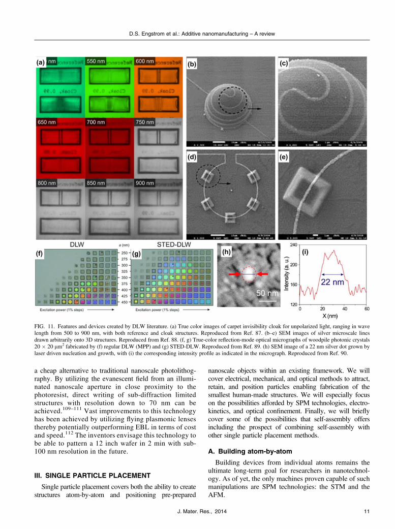
DLW of nanoscale features is capable of building 3Dstructures from the ground up in a rapid and facilemanner (see Fig. 11). Although DLW is a resist-basedfabrication method and therefore requires an additionaldevelopment step, it is very similar in nature to additivenanofabrication because the fabricated structures havetheir final shape without following deposition or etchsteps. Laser driven 3D nanofabrication is best achieved bymultiphoton polymerization (MPP).91,92 In MPP, theconcentration of photons in the neck of a femtosecondpulse of a laser beam allows for the controlled photo-polymerization of a targeted volume (or voxel) in a pho-toresist. Development of this resin allows 3D features to bewritten at typically 10–500 lm/s with nanoscale resolu-tion. This is particularly useful for fabricating 3D photonicstructures87,92,93 that would otherwise be extremelyexpensive and difficult to manufacture with the alignment
of sequential 2D layers via traditional lithography. Thesuccessful commercialization of this technology by com-panies like Nanoscribe GmbH has enabled photonicsresearchers to investigate new applications in 3D withinvisibility cloaks,87,93 Gecko-mimicking surfaces,94 and3D data storage95 among other impressive achievements inrecent years.
The range of materials that can be polymerized forMPP nanofabrication is a significant challenge for mate-rials science to explore. For solid structures, advancedcomposites or solutions that respond to MPP have beendemonstrated, resulting in structures of vanadium96 andsilver.90 The simplest approach to avoid this is to use thesurfaces of 3D polymer structures as scaffolds for thedeposition of other materials. Metallization of such scaf-folds by ALD or electroless plating has been shown towork for metallic photonic crystals97 and metamaterials.98
The polymer structures written can also be used for castingof 3D structures from other materials like titania.99
Maximizing the resolution of MPP is of course animportant goal, with Abbe’s diffraction limit representingthe typical limit. A recent review100 summarized theadvances in sub-diffraction limit DLW. As an exampleCao et al. achieved the highest resolution of this techniqueto date with 40 nm dots in a highly sensitive photoresin101
and 22 nm silver dots by laser activated nanoparticlegrowth.90 These results are extremely impressive, but thehigh resolution was only achievable for individual dots.When continuous structures were attempted, a larger linewidth of 130 nm was achieved at a comparatively lowscanning speed of 3 lm/s.101 Stimulated emissiondepletion (STED), which has achieved 5.8 6 0.8 nmresolution in microscopy,102 is also being put forward asa promising route to sub-diffraction MPP. It has beeneffective in building 3D nanoscale structures over a largearea87,99 and shows significant improvement over regularMPP for 175 nm parallel structures89 achieving 65 nm linewidths103 whilst scanning at 100 lm/s.
DLW is also able to create a wider range of features in2D by initiating reactions locally with the input of energyfrom the laser. This includes reducing graphite oxide todraw supercapacitors,104 the laser-induced chemical vapordeposition of graphene on Ni,105 the growth ofCNTs,106,107 and the electroless plating of silver.88 In-tegrating these technologies could enable the entirely laserdriven fabrication of carbon nanotechnologies. Othermethods of laser writing like sintering of a silver nano-particle ink108 could work well for large scale patterning ofelectrodes. In these cases, higher scan speeds up to1000 mm/s have been shown to reduce the features linewidth and height to below 5 lm and 50 nm, respectively,with an increasingly high surface roughness an unfortu-nate consequence.
Although technically not an additive manufacturingmethod, scanning near-field photolithography provides
D.S. Engstrom et al.: Additive nanomanufacturing – A review
J. Mater. Res., 201410
a cheap alternative to traditional nanoscale photolithog-raphy. By utilizing the evanescent field from an illumi-nated nanoscale aperture in close proximity to thephotoresist, direct writing of sub-diffraction limitedstructures with resolution down to 70 nm can beachieved.109–111 Vast improvements to this technologyhas been achieved by utilizing flying plasmonic lensesthereby potentially outperforming EBL in terms of costand speed.112 The inventors envisage this technology tobe able to pattern a 12 inch wafer in 2 min with sub-100 nm resolution in the future.
III. SINGLE PARTICLE PLACEMENT
Single particle placement covers both the ability to createstructures atom-by-atom and positioning pre-prepared
nanoscale objects within an existing framework. We willcover electrical, mechanical, and optical methods to attract,retain, and position particles enabling fabrication of thesmallest human-made structures. We will especially focuson the possibilities afforded by SPM technologies, electro-kinetics, and optical confinement. Finally, we will brieflycover some of the possibilities that self-assembly offersincluding the prospect of combining self-assembly withother single particle placement methods.
A. Building atom-by-atom
Building devices from individual atoms remains theultimate long-term goal for researchers in nanotechnol-ogy. As of yet, the only machines proven capable of suchmanipulations are SPM technologies: the STM and theAFM.
FIG. 11. Features and devices created by DLW literature. (a) True color images of carpet invisibility cloak for unpolarized light, ranging in wavelength from 500 to 900 nm, with both reference and cloak structures. Reproduced from Ref. 87. (b–e) SEM images of silver microscale linesdrawn arbitrarily onto 3D structures. Reproduced from Ref. 88. (f, g) True-color reflection-mode optical micrographs of woodpile photonic crystals20 � 20 lm2 fabricated by (f) regular DLW (MPP) and (g) STED-DLW. Reproduced from Ref. 89. (h) SEM image of a 22 nm silver dot grown bylaser driven nucleation and growth, with (i) the corresponding intensity profile as indicated in the micrograph. Reproduced from Ref. 90.
D.S. Engstrom et al.: Additive nanomanufacturing – A review
11J. Mater. Res., 2014

In arguably the most well-known use of a STM,researchers at IBM pioneered atomic manipulation byrearranging Xe atoms on a Ni substrate to spell out“IBM” [Figs. 12(a) and 12(b)].27 AFM manipulation ofatoms even advanced the technology up to room temper-atures, achieving the atomic switching of adatoms113
[see Figs. 12(c)–12(e)] or the more unconventional verticalinterchange of atoms between the surface and the tip.114
These approaches demonstrate the impressive atomic limit ofthe current technology and are used frequently in fundamen-tal research to position and characterize atoms and mole-cules.115–117 Although STM probes do not offer highthroughput, it is the most precise nanomanufacturing toolavailable and is being used to fabricate some of the first singleatom transistors for quantum computing.118 The processknown as STM lithography involves selectively driving the
FIG. 12. (a, b) STM images of the arrangement of Xe atoms on a Ni surface (a) before and (b) after manipulation with the STM probe. Reproducedfrom Ref. 27. Each letter is 5 nm from top to bottom. (c–e) A sequence of AFM images showing the lateral manipulation of substitutional Sn adatomsin a Ge surface by inducing adatom exchange at room temperature with an AFM probe tip. Reproduced fromRef. 113. One of these manipulation stepsis presented (c) before and (d) after adatom exchange of the brighter Sn atoms and (c) shows the final AFM image of the Sn atoms rearranged to givethe atomic symbol Sn. (c) and (d) are 4.6 � 4.6 nm2 and (e) is 7.7 � 7.7 nm2.
D.S. Engstrom et al.: Additive nanomanufacturing – A review
J. Mater. Res., 201412
electrical desorption of hydrogen atoms from the surface ofhydrogen passivated silicon and letting a phosphorus atomdiffuse through the window formed by the missing hydrogenatom.
B. Nanoparticle manipulation
The visual image of additive manufacturing is oftena robotic arm picking up a component and inserting itinto another component. This literal understanding ofAM has been miniaturized and microscale electrother-mally actuated robotic arms have been used to break offvertically aligned CNTs and place them onto surfaces,such as on the tip of an AFM probe.120,121 With arms likethese, even nanotubes of tens of nanometers in diametercan be gripped and moved.122 Although this is a processthat struggles to manipulate smaller nano-objects andoperates at very high temperatures for many applications,microgrippers challenged the idea that some objects arejust too small to pick up and place in a desired location.
The AFM offers more flexibility to researchers; it iscapable of maneuvering a diverse range of materials fromnanoparticles123,124 and atoms113,114 to biological cells,125
be it under vacuum or immersed in liquid. The rudimen-tary method of nanoparticle manipulation with an AFMuses the probe tip to push, pull, and slide nanoparticlesaround on a substrate, positioning them into desiredconfigurations.126 By moving the probe on a vectorthrough the center of the targeted particle in the desireddirection, the nanoparticle can be moved across the surfaceby the interaction forces between the nanoparticle and tipapex. Unfortunately, these methods have very lowthroughput and require the operator to constantly imagethe surface to track the particle’s progress. The accuracy ofeach iterative process has a high uncertainty, since theparticle will be likely skewed to one side or the other of theintended path if not pushed precisely in the center, whichbecomes more likely for smaller particles. Recognizingthese flaws, Kim et al. pioneered a novel method ofmanipulating nanoparticles whilst simultaneously imag-ing the surface.123 They relied on the principle that staticfriction is time-dependant and will increase if two surfacesare left inert. They studied 15 nm Au nanoparticles onplanar quartz surfaces. One nanoparticle was initially“kicked” to reduce the standing friction, before the surfacewas scanned at a sufficiently high rate (;7 Hz) with theAFM in tapping mode. The kicked particle moved acrossthe surface in a direction perpendicular to the scanningaxis, with motion ceasing abruptly and precisely when thescan speed was dropped below the threshold. Thisphenomenon resulted from the mechanical force the probetip exerts on the nanoparticle on each pass pushing it alongthe surface, which also created ghost images of the particlegiving an intuitive picture of its path. Critically, this resultwas only observed for the nanoparticle that was initially
kicked, validating the hypothesis regarding the importanceof the change in friction. To demonstrate how effectivethis technique was, they ran comparison studies with theexisting manipulation method, reporting that efficiencywas improved by a factor of 5–10 whilst achieving at leastparity of precision. Using this method of nanomanipula-tion, the same group has managed to characterize thecoupling between a gold nanoparticle in a hybrid nano-structure with a semiconductor quantum dot,124 demon-strating the usefulness of this technique to more efficientmechanical manipulation. Testing with other particles andnanoscale objects will be needed to see how transferrablethe method can be.
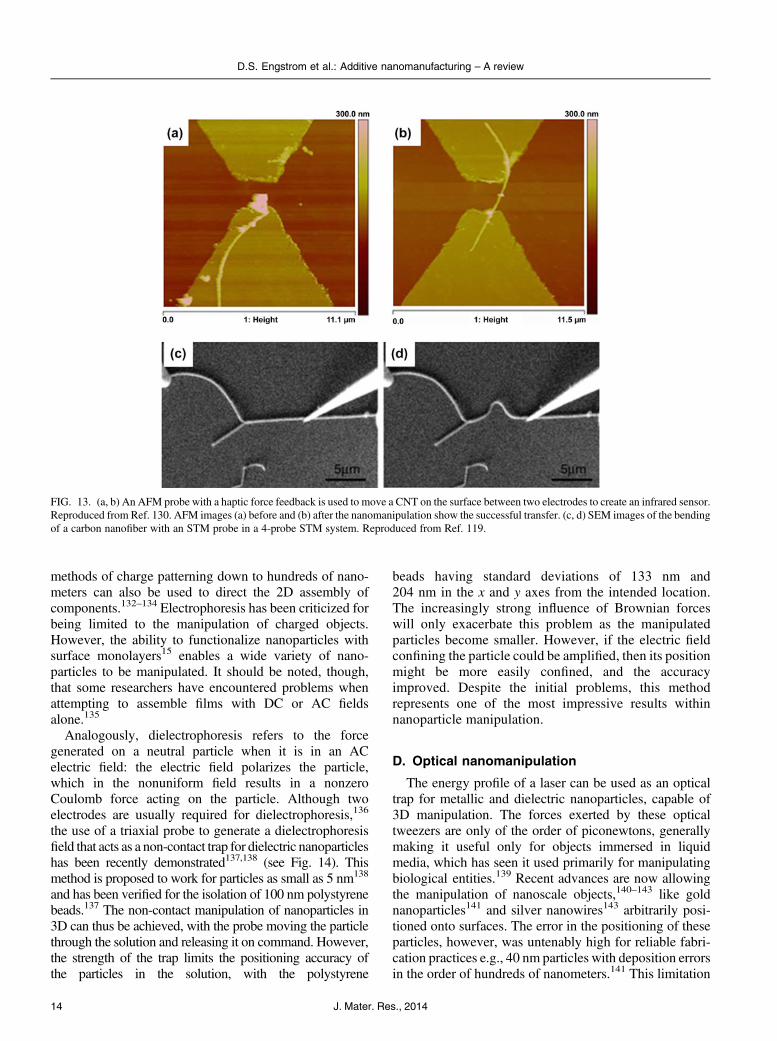
In an alternative approach to circumventing the unreliablemanipulation of objects with the AFM, Li et al. havedeveloped a system that generates real-time force feedbackto the operator through a haptic joystick,127 that is also usedto update AFM scans of the surface.128 The development ofthis technology129 has culminated in a corrective fabricationtechnique, wherein CNTs are assembled near electrodes bydielectrophoresis before being repositioned to bridge theelectrode gap [see Figs. 13(a) and 13(b)].130 Using thistechnique of nanorobotic manipulation, they were able tobuild and test single-walled, multi-walled, and bundles ofCNTs onto electrodes to operate as functional infraredsensors.
In many cases, visualization is realized by building themanipulators into an SEM setup to give operators real-time visualization of the objects they are controlling. Thisis a common combination for microgrippers, but has alsobeen used using SPM probes. For example, in the workby Qin et al., carbon fibers are pushed, bent, burnt, andbroken under the real-time observations of the SEM [seeFigs. 13(c) and 13(d)]. The combination of these machinescould prove useful to researchers, who can take measure-ments and images of their devices during processes drivenby the probe tips.
The need for active engagement of a human operatorwith these different mechanisms to ensure successfulmanipulation of nano-objects makes industrial adaptationimpractical at present, with the best applications availablein pure research. This problem may be solved if recogni-tion and positioning of components can be automated bysoftware. Additionally, mechanical manipulations are pri-marily limited to the 2D rearrangement of existing nano-objects, which limits the scope for 3D manufacturing.
C. Electrokinetic nanomanipulation
A force can be exerted on charged objects in solutionwhen in a DC electric field, an effect known aselectrophoresis, which allows for straightforward manip-ulation of particles toward charged surfaces. Thesecharged surfaces are easily created by the application ofa DC voltage between electrodes,131 although alternative
D.S. Engstrom et al.: Additive nanomanufacturing – A review
13J. Mater. Res., 2014
methods of charge patterning down to hundreds of nano-meters can also be used to direct the 2D assembly ofcomponents.132–134 Electrophoresis has been criticized forbeing limited to the manipulation of charged objects.However, the ability to functionalize nanoparticles withsurface monolayers15 enables a wide variety of nano-particles to be manipulated. It should be noted, though,that some researchers have encountered problems whenattempting to assemble films with DC or AC fieldsalone.135
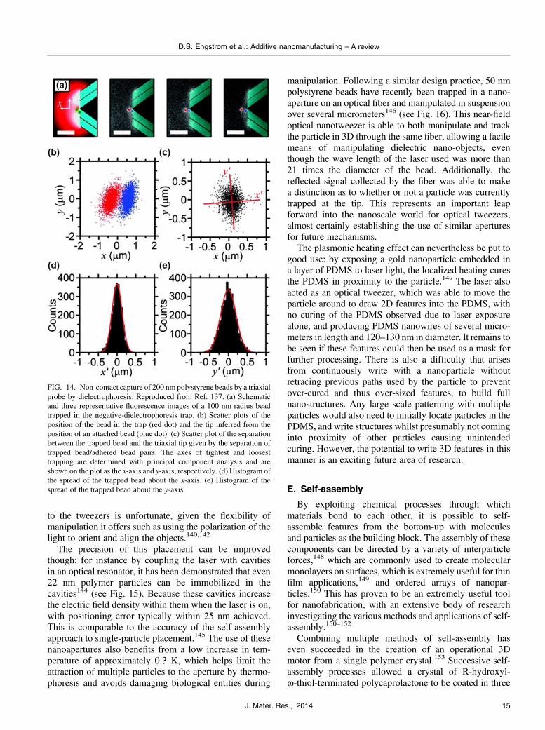
Analogously, dielectrophoresis refers to the forcegenerated on a neutral particle when it is in an ACelectric field: the electric field polarizes the particle,which in the nonuniform field results in a nonzeroCoulomb force acting on the particle. Although twoelectrodes are usually required for dielectrophoresis,136
the use of a triaxial probe to generate a dielectrophoresisfield that acts as a non-contact trap for dielectric nanoparticleshas been recently demonstrated137,138 (see Fig. 14). Thismethod is proposed to work for particles as small as 5 nm138
and has been verified for the isolation of 100 nm polystyrenebeads.137 The non-contact manipulation of nanoparticles in3D can thus be achieved, with the probe moving the particlethrough the solution and releasing it on command. However,the strength of the trap limits the positioning accuracy ofthe particles in the solution, with the polystyrene
beads having standard deviations of 133 nm and204 nm in the x and y axes from the intended location.The increasingly strong influence of Brownian forceswill only exacerbate this problem as the manipulatedparticles become smaller. However, if the electric fieldconfining the particle could be amplified, then its positionmight be more easily confined, and the accuracyimproved. Despite the initial problems, this methodrepresents one of the most impressive results withinnanoparticle manipulation.
D. Optical nanomanipulation
The energy profile of a laser can be used as an opticaltrap for metallic and dielectric nanoparticles, capable of3D manipulation. The forces exerted by these opticaltweezers are only of the order of piconewtons, generallymaking it useful only for objects immersed in liquidmedia, which has seen it used primarily for manipulatingbiological entities.139 Recent advances are now allowingthe manipulation of nanoscale objects,140–143 like goldnanoparticles141 and silver nanowires143 arbitrarily posi-tioned onto surfaces. The error in the positioning of theseparticles, however, was untenably high for reliable fabri-cation practices e.g., 40 nm particles with deposition errorsin the order of hundreds of nanometers.141 This limitation
FIG. 13. (a, b) An AFM probe with a haptic force feedback is used to move a CNT on the surface between two electrodes to create an infrared sensor.Reproduced from Ref. 130. AFM images (a) before and (b) after the nanomanipulation show the successful transfer. (c, d) SEM images of the bendingof a carbon nanofiber with an STM probe in a 4-probe STM system. Reproduced from Ref. 119.
D.S. Engstrom et al.: Additive nanomanufacturing – A review
J. Mater. Res., 201414
to the tweezers is unfortunate, given the flexibility ofmanipulation it offers such as using the polarization of thelight to orient and align the objects.140,142
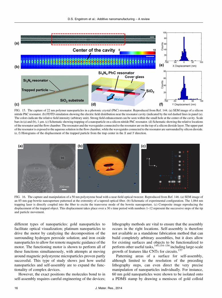
The precision of this placement can be improvedthough: for instance by coupling the laser with cavitiesin an optical resonator, it has been demonstrated that even22 nm polymer particles can be immobilized in thecavities144 (see Fig. 15). Because these cavities increasethe electric field density within them when the laser is on,with positioning error typically within 25 nm achieved.This is comparable to the accuracy of the self-assemblyapproach to single-particle placement.145 The use of thesenanoapertures also benefits from a low increase in tem-perature of approximately 0.3 K, which helps limit theattraction of multiple particles to the aperture by thermo-phoresis and avoids damaging biological entities during
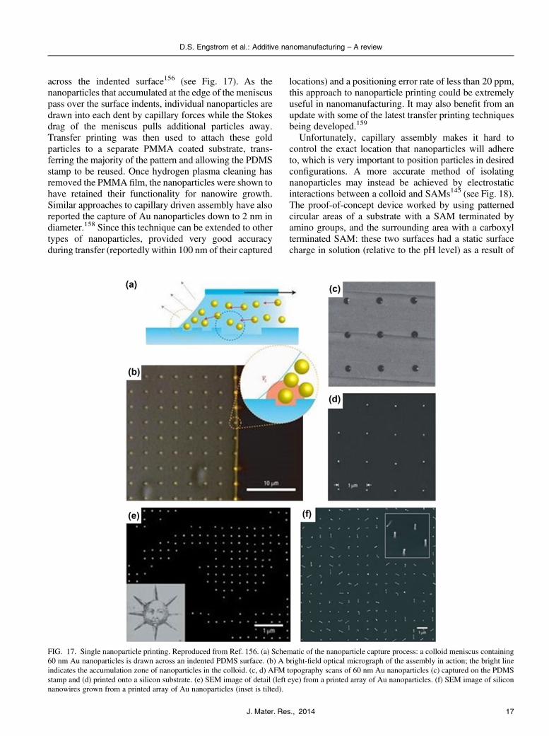
manipulation. Following a similar design practice, 50 nmpolystyrene beads have recently been trapped in a nano-aperture on an optical fiber and manipulated in suspensionover several micrometers146 (see Fig. 16). This near-fieldoptical nanotweezer is able to both manipulate and trackthe particle in 3D through the same fiber, allowing a facilemeans of manipulating dielectric nano-objects, eventhough the wave length of the laser used was more than21 times the diameter of the bead. Additionally, thereflected signal collected by the fiber was able to makea distinction as to whether or not a particle was currentlytrapped at the tip. This represents an important leapforward into the nanoscale world for optical tweezers,almost certainly establishing the use of similar aperturesfor future mechanisms.
The plasmonic heating effect can nevertheless be put togood use: by exposing a gold nanoparticle embedded ina layer of PDMS to laser light, the localized heating curesthe PDMS in proximity to the particle.147 The laser alsoacted as an optical tweezer, which was able to move theparticle around to draw 2D features into the PDMS, withno curing of the PDMS observed due to laser exposurealone, and producing PDMS nanowires of several micro-meters in length and 120–130 nm in diameter. It remains tobe seen if these features could then be used as a mask forfurther processing. There is also a difficulty that arisesfrom continuously write with a nanoparticle withoutretracing previous paths used by the particle to preventover-cured and thus over-sized features, to build fullnanostructures. Any large scale patterning with multipleparticles would also need to initially locate particles in thePDMS, and write structures whilst presumably not cominginto proximity of other particles causing unintendedcuring. However, the potential to write 3D features in thismanner is an exciting future area of research.
E. Self-assembly
By exploiting chemical processes through whichmaterials bond to each other, it is possible to self-assemble features from the bottom-up with moleculesand particles as the building block. The assembly of thesecomponents can be directed by a variety of interparticleforces,148 which are commonly used to create molecularmonolayers on surfaces, which is extremely useful for thinfilm applications,149 and ordered arrays of nanopar-ticles.150 This has proven to be an extremely useful toolfor nanofabrication, with an extensive body of researchinvestigating the various methods and applications of self-assembly.150–152
Combining multiple methods of self-assembly haseven succeeded in the creation of an operational 3Dmotor from a single polymer crystal.153 Successive self-assembly processes allowed a crystal of R-hydroxyl-x-thiol-terminated polycaprolactone to be coated in three
FIG. 14. Non-contact capture of 200 nm polystyrene beads by a triaxialprobe by dielectrophoresis. Reproduced from Ref. 137. (a) Schematicand three representative fluorescence images of a 100 nm radius beadtrapped in the negative-dielectrophoresis trap. (b) Scatter plots of theposition of the bead in the trap (red dot) and the tip inferred from theposition of an attached bead (blue dot). (c) Scatter plot of the separationbetween the trapped bead and the triaxial tip given by the separation oftrapped bead/adhered bead pairs. The axes of tightest and loosesttrapping are determined with principal component analysis and areshown on the plot as the x-axis and y-axis, respectively. (d) Histogram ofthe spread of the trapped bead about the x-axis. (e) Histogram of thespread of the trapped bead about the y-axis.
D.S. Engstrom et al.: Additive nanomanufacturing – A review
15J. Mater. Res., 2014
different types of nanoparticles: gold nanoparticles tofacilitate optical visualization; platinum nanoparticles todrive the motor by catalyzing the decomposition of thesurrounding hydrogen peroxide solution; and iron oxidenanoparticles to allow for remote magnetic guidance of themotor. The functioning motor is shown to perform all ofthese functions simultaneously, with attempts at movingaround magnetic polystyrene microparticles proven partlysuccessful. This type of study shows just how usefulnanoparticles and self-assembly are to expand the func-tionality of complex devices.
However, the exact positions the molecules bond to inself-assembly requires careful engineering of the devices;
lithography methods are vital to ensure that the assemblyoccurs in the right locations. Self-assembly is thereforenot available as a standalone fabrication method that canbuild completely arbitrary assemblies, but it does allowfor existing surfaces and objects to be functionalized toperform other useful tasks,149,154–156 including large-scalegrowth of features like CNTs for circuits.157
Patterning areas of a surface for self-assembly,although limited to the resolution of the precedinglithography steps, can even direct the very precisemanipulation of nanoparticles individually. For instance,60 nm gold nanoparticles were shown to be isolated ontoa PDMS stamp by drawing a meniscus of gold colloid
FIG. 15. The capture of 22 nm polymer nanoparticles in a photonic crystal (PhC) resonator. Reproduced from Ref. 144. (a) SEM image of a siliconnitride PhC resonator. (b) FDTD simulation showing the electric field distribution near the resonator cavity (indicated by the red dashed lines in panel (a).The colors indicate the relative field intensity (arbitrary unit). Strong field enhancement can be seen within the small hole at the center of the cavity. Scalebars in (a) and (b), 1 lm. (c) Schematic showing trapping of a nanoparticle on a silicon nitride PhC resonator. (d) Schematic showing the relative locationsof the resonator and theflow chamber. The resonator and thewaveguides connected to the resonator are on the top of a silicon dioxide layer. The upper partof the resonator is exposed to the aqueous solution in the flowchamber, while thewaveguides connected to the resonator are surrounded by silicon dioxide.(e, f) Histograms of the displacement of the trapped particle from the trap center in the X and Y direction.
FIG. 16. The capture and manipulation of a 50 nm polystyrene bead with a near-field optical tweezer. Reproduced from Ref. 146. (a) SEM image ofan 85-nm-gap bowtie nanoaperture patterned at the extremity of a tapered optical fiber. (b) Schematic of experimental configuration. The 1,064 nmtrapping laser is directly coupled into the fiber to excite the transverse mode of the bowtie nanoaperture. (c) Composite image reproducing thedisplacement of the trapped object. This displacement takes place over a 30 s time period with numbers 1–12 represent the successive steps of the tipand particle movement.
D.S. Engstrom et al.: Additive nanomanufacturing – A review
J. Mater. Res., 201416
across the indented surface156 (see Fig. 17). As thenanoparticles that accumulated at the edge of the meniscuspass over the surface indents, individual nanoparticles aredrawn into each dent by capillary forces while the Stokesdrag of the meniscus pulls additional particles away.Transfer printing was then used to attach these goldparticles to a separate PMMA coated substrate, trans-ferring the majority of the pattern and allowing the PDMSstamp to be reused. Once hydrogen plasma cleaning hasremoved the PMMA film, the nanoparticles were shown tohave retained their functionality for nanowire growth.Similar approaches to capillary driven assembly have alsoreported the capture of Au nanoparticles down to 2 nm indiameter.158 Since this technique can be extended to othertypes of nanoparticles, provided very good accuracyduring transfer (reportedly within 100 nm of their captured
locations) and a positioning error rate of less than 20 ppm,this approach to nanoparticle printing could be extremelyuseful in nanomanufacturing. It may also benefit from anupdate with some of the latest transfer printing techniquesbeing developed.159
Unfortunately, capillary assembly makes it hard tocontrol the exact location that nanoparticles will adhereto, which is very important to position particles in desiredconfigurations. A more accurate method of isolatingnanoparticles may instead be achieved by electrostaticinteractions between a colloid and SAMs145 (see Fig. 18).The proof-of-concept device worked by using patternedcircular areas of a substrate with a SAM terminated byamino groups, and the surrounding area with a carboxylterminated SAM: these two surfaces had a static surfacecharge in solution (relative to the pH level) as a result of
FIG. 17. Single nanoparticle printing. Reproduced from Ref. 156. (a) Schematic of the nanoparticle capture process: a colloid meniscus containing60 nm Au nanoparticles is drawn across an indented PDMS surface. (b) A bright-field optical micrograph of the assembly in action; the bright lineindicates the accumulation zone of nanoparticles in the colloid. (c, d) AFM topography scans of 60 nm Au nanoparticles (c) captured on the PDMSstamp and (d) printed onto a silicon substrate. (e) SEM image of detail (left eye) from a printed array of Au nanoparticles. (f) SEM image of siliconnanowires grown from a printed array of Au nanoparticles (inset is tilted).
D.S. Engstrom et al.: Additive nanomanufacturing – A review
17J. Mater. Res., 2014
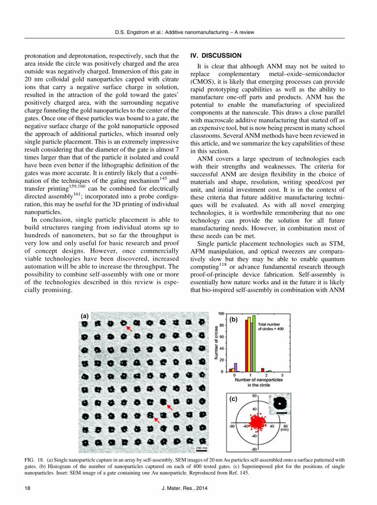
protonation and deprotonation, respectively, such that thearea inside the circle was positively charged and the areaoutside was negatively charged. Immersion of this gate in20 nm colloidal gold nanoparticles capped with citrateions that carry a negative surface charge in solution,resulted in the attraction of the gold toward the gates’positively charged area, with the surrounding negativecharge funneling the gold nanoparticles to the center of thegates. Once one of these particles was bound to a gate, thenegative surface charge of the gold nanoparticle opposedthe approach of additional particles, which insured onlysingle particle placement. This is an extremely impressiveresult considering that the diameter of the gate is almost 7times larger than that of the particle it isolated and couldhave been even better if the lithographic definition of thegates was more accurate. It is entirely likely that a combi-nation of the techniques of the gating mechanism145 andtransfer printing159,160 can be combined for electricallydirected assembly161; incorporated into a probe configu-ration, this may be useful for the 3D printing of individualnanoparticles.
In conclusion, single particle placement is able tobuild structures ranging from individual atoms up tohundreds of nanometers, but so far the throughput isvery low and only useful for basic research and proofof concept designs. However, once commerciallyviable technologies have been discovered, increasedautomation will be able to increase the throughput. Thepossibility to combine self-assembly with one or moreof the technologies described in this review is espe-cially promising.
IV. DISCUSSION
It is clear that although ANM may not be suited toreplace complementary metal–oxide–semiconductor(CMOS), it is likely that emerging processes can providerapid prototyping capabilities as well as the ability tomanufacture one-off parts and products. ANM has thepotential to enable the manufacturing of specializedcomponents at the nanoscale. This draws a close parallelwith macroscale additive manufacturing that started off asan expensive tool, but is now being present in many schoolclassrooms. Several ANMmethods have been reviewed inthis article, and we summarize the key capabilities of thesein this section.
ANM covers a large spectrum of technologies eachwith their strengths and weaknesses. The criteria forsuccessful ANM are design flexibility in the choice ofmaterials and shape, resolution, writing speed/cost perunit, and initial investment cost. It is in the context ofthese criteria that future additive manufacturing techni-ques will be evaluated. As with all novel emergingtechnologies, it is worthwhile remembering that no onetechnology can provide the solution for all futuremanufacturing needs. However, in combination most ofthese needs can be met.
Single particle placement technologies such as STM,AFM manipulation, and optical tweezers are compara-tively slow but they may be able to enable quantumcomputing118 or advance fundamental research throughproof-of-principle device fabrication. Self-assembly isessentially how nature works and in the future it is likelythat bio-inspired self-assembly in combination with ANM
FIG. 18. (a) Single nanoparticle capture in an array by self-assembly. SEM images of 20 nmAu particles self-assembled onto a surface patterned withgates. (b) Histogram of the number of nanoparticles captured on each of 400 tested gates. (c) Superimposed plot for the positions of singlenanoparticles. Inset: SEM image of a gate containing one Au nanoparticle. Reproduced from Ref. 145.
D.S. Engstrom et al.: Additive nanomanufacturing – A review
J. Mater. Res., 201418
will create novel structures on a large scale. So far, self-assembly is in its infancy but as a tool to controlwettability72 and adhesion16 or guide charged particles145
SAMs have found extensive use.162
DPN has been shown to offer an excellent selection ofboth organic and inorganic materials with sub-50 nmresolution. In the course of the development of thistechnology, the traditional cantilever structure has beenreplaced by cantilever-free systems and arrays of probes. Sofar, the resolution is limited by the size of both the tip andthe meniscus forming between the tip and the substrate. Formany biological applications, the current resolution isadequate; in fact, DPN is a powerful research tool formanipulating cells at subcellular resolution163 and changingthe growth conditions for these cells. This resolution is,however, not sufficient for the future of IC manufacturing,but closely related lithography methods such as local anodicoxidation reach sub-10 nm resolution164 proving that betterresolution is possible with DPN when combined with anelectrically driven reaction. DPN has so far been a two-dimensional lithography technique but the technology is veryflexible with an inbuilt imaging capability and extending itinto the third dimension seems plausible in the near future.
Electrohydrodynamic (EHD) jet printing has gonethrough a rapid development in the last couple of yearswith resolutions now reaching sub-50 nm72,77 or sub-10 nm when combined with block copolymer technolo-gies.73 The writing speed is unparalleled when comparedto other additive manufacturing technologies presentedhere (see Table I) and is comparable to the writing speed ofEBL. Additionally, EHD jet printing is capable of printingin three dimensions72 and because the material is de-posited through a solvent, a wide range of materials can beavailable. The equipment requirements are basic, soequipment cost can be kept low. The main challengesare nozzle clogging and layer-to-layer alignment but theseare not insurmountable problems making EHD jet printinga promising candidate for future ANM.
DLW offers great flexibility and was one of the firsttechnologies capable of 3D manufacturing at the nanoscale.
It has proven invaluable for fabrication of 3D photonicstructures and has already had commercial success. Despitethis success, DLW has drawbacks particularly becausematerial selection is still limited in spite of it beinga relatively mature technology.
Direct write nanomanufacturing is still not able toproduce the billions of structures needed for the ICindustry, but neither is macroscale additive manufacturingable to compete with the cost per unit of injection moldingand other mass-fabrication methods. Macroscale additivemanufacturing first found a home in niche areas of dentaland medical care, aerospace, automotive, and entertain-ment; nevertheless, macroscale additive manufacturing ison the rise and the market is predicted to double from 2011to 2015.1 ANM will have to start out with markets smallerthan IC manufacturing and the smaller investment neededfor ANM equipment will help this development.
Currently an IC manufacturing plant costs around$9 billion; an ANM unit at ,$500,000 would be trans-formational for small and medium size firms to own theirmanufacturing facilities. Additionally, the way designersthink will change as 3D structures become readily avail-able and the low material waste enables the use ofexpensive materials such as proteins in biosensors. Thereis also a potential environmental gain to using ANM overplanar device fabrication as a traditionally built 2 g siliconchip requires 1.6 kg of fossil fuel, 73 g of chemicals, and32 kg of water.20,168 Research into additive nanomanu-facture could focus on cutting this environmental impact,for example by eliminating waste by directly placingmaterials where needed. Additionally, ideas that previ-ously had no future because the market did not require themillions of sold units needed to break-even may nowbecome viable. The unit price of direct writing does notdepend on the density of the printed structures, as is thecase for planar device fabrication, but rather depends onthe total printed area. For a chemical or biomarker sensor,the detector area might be much smaller than the minimumdie size and planar manufacturing could become pro-hibitively expensive.
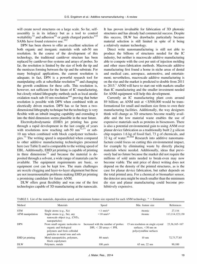
TABLE I. List of the materials, deposition speed, and minimum feature size reported for each ANM technology. * 5 Estimated.
Method Materials Speed Min. feature size References
STM Single atoms (e.g., Xe) ,1 nm/s* Atomic 27,116AFM manipulation Single atoms (e.g., Sn), any
nanoscale object (e.g., CNTs,nanoparticles)
,10 nm/s* Atomic 113,114,123,130
DPN From small organic molecules toorganic and biologicalpolymers and from colloidalparticles to metal ions and sols
Increased with the number of probes:DPL , 2D arrays , PPL
15 nm resolution on single crystalsurfaces, ,50 nm onpolycrystalline surfaces
23,36,165–167
EHD jet printing Metal nanoparticles, polymers,block copolymers
80 mm/s 10 nm 72,73,77,85
DLW Polymers, metals 100 lm/s 65 nm, 22 nm 90,100
D.S. Engstrom et al.: Additive nanomanufacturing – A review
19J. Mater. Res., 2014
The aspect of resolution as compared to semiconductormanufacturing is also seeing progress; the resolution ofsome of these techniques has reached a level where it cancompete with that of EUV-lithography. They arewell suited to a range of materials, not just “CMOS-compatible” materials; Table I summarizes a subset of theavailable materials possible in each of these technologies.
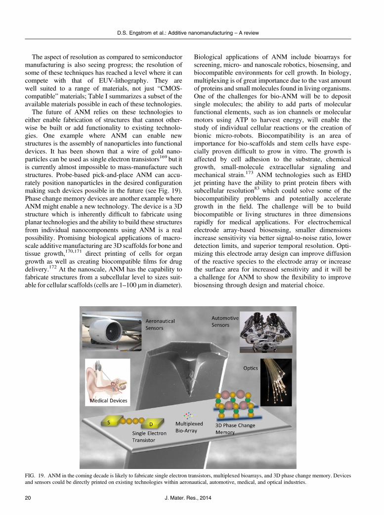
The future of ANM relies on these technologies toeither enable fabrication of structures that cannot other-wise be built or add functionality to existing technolo-gies. One example where ANM can enable newstructures is the assembly of nanoparticles into functionaldevices. It has been shown that a wire of gold nano-particles can be used as single electron transistors169 but itis currently almost impossible to mass-manufacture suchstructures. Probe-based pick-and-place ANM can accu-rately position nanoparticles in the desired configurationmaking such devices possible in the future (see Fig. 19).Phase change memory devices are another example whereANM might enable a new technology. The device is a 3Dstructure which is inherently difficult to fabricate usingplanar technologies and the ability to build these structuresfrom individual nanocomponents using ANM is a realpossibility. Promising biological applications of macro-scale additive manufacturing are 3D scaffolds for bone andtissue growth,170,171 direct printing of cells for organgrowth as well as creating biocompatible films for drugdelivery.172 At the nanoscale, ANM has the capability tofabricate structures from a subcellular level to sizes suit-able for cellular scaffolds (cells are 1–100 lm in diameter).
Biological applications of ANM include bioarrays forscreening, micro- and nanoscale robotics, biosensing, andbiocompatible environments for cell growth. In biology,multiplexing is of great importance due to the vast amountof proteins and small molecules found in living organisms.One of the challenges for bio-ANM will be to depositsingle molecules; the ability to add parts of molecularfunctional elements, such as ion channels or molecularmotors using ATP to harvest energy, will enable thestudy of individual cellular reactions or the creation ofbionic micro-robots. Biocompatibility is an area ofimportance for bio-scaffolds and stem cells have espe-cially proven difficult to grow in vitro. The growth isaffected by cell adhesion to the substrate, chemicalgrowth, small-molecule extracellular signaling andmechanical strain.173 ANM technologies such as EHDjet printing have the ability to print protein fibers withsubcellular resolution83 which could solve some of thebiocompatibility problems and potentially accelerategrowth in the field. The challenge will be to buildbiocompatible or living structures in three dimensionsrapidly for medical applications. For electrochemicalelectrode array-based biosensing, smaller dimensionsincrease sensitivity via better signal-to-noise ratio, lowerdetection limits, and superior temporal resolution. Opti-mizing this electrode array design can improve diffusionof the reactive species to the electrode array or increasethe surface area for increased sensitivity and it will bea challenge for ANM to show the flexibility to improvebiosensing through design and material choice.
FIG. 19. ANM in the coming decade is likely to fabricate single electron transistors, multiplexed bioarrays, and 3D phase change memory. Devicesand sensors could be directly printed on existing technologies within aeronautical, automotive, medical, and optical industries.
D.S. Engstrom et al.: Additive nanomanufacturing – A review
J. Mater. Res., 201420
Direct writing of graphene might also be possible inthe future by allowing an AFM tip coated with graphite toslide over a surface, thereby leaving a nanoribbon/monolayer of exfoliated graphene. This would be animprovement of the results by Zhang et al.174 who useda mounted graphite block on the cantilever as the tip of anAFM to transfer thin graphite samples onto a SiO2/Sisubstrate. “Writing” with the nanopencil yielded slices ofgraphite just a few tens of atomic layers thick, therebyalmost succeeding in direct writing of graphene. This couldenable device fabrication and repairing or modification ofexisting circuits to tailor functionality. Other areas in whichANM can solve fabrication challenges in the future arephotonic crystals, metamaterials such as negative refractiveindex materials and invisibility cloaks, electrochemicalreactors, and high-density electronics.
ANM can also be used to add functionality to existingstructures in the future. For example, electronics could beprinted directly at the end of an optical fiber therebyintegrating optics and electronics in ways never seenbefore, and sensors can be printed directly onto engineparts or medical devices. ANM would also enable fullyintegrated devices including electronic, optical, and bio-chemical elements.
In conclusion, we have reviewed both single particleplacement and direct writing technologies able tocreate sub-100 nm structures. We have especiallyfocused on their ability to create heterogenous struc-tures from multiple materials and the possibility toextend fabrication into the third dimension. We iden-tified single particle placement technologies such asSTM, AFM manipulation, and optical tweezers asenablers of technological advances but not as futuremanufacturing tools. Direct writing technologies, onthe other hand, offer a much more promising future ofdesign flexibility, high resolution, and high throughput.DLW offers high geometrical flexibility and mediumthroughput but currently suffers from a poor selectionof materials. DPN is a reasonably mature technology witha wide material selection and promises of sub-10 nm reso-lution. The technology can be scaled up and currently themain challenges are to print in three dimensions andcombine more functional materials. EHD jet printing is asimple and inexpensive technology that offers writingspeeds comparable with e-beam lithography with highresolution (;20 nm) and great material choice. Addition-ally, 3D structures of only 50 nm wide have been printedproving the possibility of true 3D ANM.
Within the next few years, we predict a rapiddevelopment of the ANM technologies presented here,especially toward 3D ANM. This new capability willinevitably lead to more innovation as new applicationsemerge. If ANM follows the development trajectory ofthe last decade, its rise as a nanoscale rapid prototypingtool will soon be imminent.
ACKNOWLEDGMENTS
This review was made possible by an EPSRCManufacturing Fellowship “Additive nanomanufacturingvia probe-based pick-and-place nanoparticle assembly,”Grant EP/J018694/1.
REFERENCES
1. F. Feenstra, M. Schaefer, O. Jay, and R. Scudamore: AdditiveManufacturing: Strategic Research Agenda. AM Platform: TheEuropean collaboration on Additive Manufacturing 1(1), 1(2013).
2. T. Boland, A. Ovsianikov, B.N. Chickov, A. Doraiswamy,R.J. Narayan, W.Y. Yeong, K.F. Leong, and C.K. Chua: Rapidprototyping of artificial tissues and medical devices. Adv. Mater.Processess 165(4), 51 (2007).
3. I. Zein, D.W. Hutmacher, K.C. Tan, and S.H. Teoh: Fuseddeposition modeling of novel scaffold architectures for tissueengineering applications. Biomaterials 23(4), 1169 (2002).
4. A.C. Arias, J.D. MacKenzie, I. McCulloch, J. Rivnay, andA. Salleo: Materials and applications for large area electronics:Solution-based approaches. Chem. Rev. 110(1), 3 (2010).
5. L.L. Zhang, X. Zhao, M.D. Stoller, Y.W. Zhu, H.X. Ji,S. Murali, Y.P. Wu, S. Perales, B. Clevenger, and R.S. Ruoff:Highly conductive and porous activated reduced grapheneoxide films for high-power supercapacitors. Nano Lett. 12(4),1806 (2012).
6. D.C. Duffy, J.C. McDonald, O.J.A. Schueller, and G.M. Whitesides:Rapid prototyping of microfluidic systems in poly(dimethylsiloxane).Anal. Chem. 70(23), 4974 (1998).
7. M.A. Unger, H.P. Chou, T. Thorsen, A. Scherer, and S.R. Quake:Monolithic microfabricated valves and pumps by multilayer softlithography. Science 288(5463), 113 (2000).
8. R. van Noort: The future of dental devices is digital. Dent. Mater.28(1), 3 (2012).
9. G. Ryan, A. Pandit, and D.P. Apatsidis: Fabrication methods ofporous metals for use in orthopaedic applications. Biomaterials27(13), 2651 (2006).
10. J. Giannatsis and V. Dedoussis: Additive fabrication technologiesapplied to medicine and health care: A review. Int. J. Adv. Manuf.Technol. 40(1–2), 116 (2009).
11. R.J. Narayan, A. Doraiswamy, D.B. Chrisey, and B.N. Chichkov:Medical prototyping using two photon polymerization. Mater.Today 13(12), 42 (2010).
12. D.D. Gu, W. Meiners, K. Wissenbach, and R. Poprawe: Laseradditive manufacturing of metallic components: Materials,processes and mechanisms. Int. Mater. Rev. 57(3), 133 (2012).
13. Y. Jang, I.H. Tambunan, H. Tak, V.D. Nguyen, T. Kang, andD. Byun: Non-contact printing of high aspect ratio Ag electrodesfor polycrystalline silicone solar cell with electrohydrodynamic jetprinting. Appl. Phys. Lett. 102(12), 123901 (2013).
14. F.C. Krebs: Fabrication and processing of polymer solar cells:A review of printing and coating techniques. Sol. Energy Mater.Sol. Cells 93(4), 394 (2009).
15. A.G. Mark, J.G. Gibbs, T.C. Lee, and P. Fischer: Hybrid nano-colloids with programmed three-dimensional shape and materialcomposition. Nat. Mater. 12(9), 802 (2013).
16. J.U. Park, M. Hardy, S.J. Kang, K. Barton, K. Adair,D.K. Mukhopadhyay, C.Y. Lee, M.S. Strano, A.G. Alleyne,J.G. Georgiadis, P.M. Ferreira, and J.A. Rogers: High-resolutionelectrohydrodynamic jet printing. Nat. Mater. 6(10), 782 (2007).
17. S.Y. Min, T.S. Kim, B.J. Kim, H. Cho, Y.Y. Noh, H. Yang,J.H. Cho, and T.W. Lee: Large-scale organic nanowirelithography and electronics. Nat. Commun. 4, 1773 (2013).
D.S. Engstrom et al.: Additive nanomanufacturing – A review
21J. Mater. Res., 2014
18. C. Wagner and N. Harned: EUV lithography: Lithography getsextreme. Nat. Photonics 4(1), 24 (2010).
19. V.R. Manfrinato, L.H. Zhang, D. Su, H.G. Duan, R.G. Hobbs,E.A. Stach, and K.K. Berggren: Resolution limits of electron-beam lithography toward the atomic scale. Nano Lett. 13(4), 1555(2013).
20. E.D. Williams, R.U. Ayres, and M. Heller: The 1.7 kilogrammicrochip: Energy and material use in the production of semi-conductor devices. Environ. Sci. Technol. 36(24), 5504 (2002).
21. P.R. Couchman and W.A. Jesser: Thermodynamic theory of sizedependence of melting temperature in metals. Nature 269(5628),481 (1977).
22. G.L. Allen, R.A. Bayles, W.W. Gile, and W.A. Jesser: Smallparticle melting of pure metals. Thin Solid Films 144(2), 297(1986).
23. D.S. Ginger, H. Zhang, and C.A.Mirkin: The evolution of dip-pennanolithography. Angew. Chem., Int. Ed. 43(1), 30 (2004).
24. G. Binnig, H. Rohrer, C. Gerber, and E. Weibel: Surface studies byscanning tunneling microscopy. Phys. Rev. Lett. 49(1), 57 (1982).
25. G. Binnig, C.F. Quate, and C. Gerber: Atomic force microscope.Phys. Rev. Lett. 56(9), 930 (1986).
26. J.K. Gimzewski and C. Joachim: Nanoscale science of singlemolecules using local probes. Science 283(5408), 1683 (1999).
27. D.M. Eigler and E.K. Schweizer: Positioning single atoms witha scanning tunnelling microscope. Nature 344(6266), 524 (1990).
28. Y. Xia and G.M. Whitesides: Soft lithography. Angew. Chem. Int.Ed. 37(5), 550 (1998).
29. J-F. Liu, S. Cruchon-Dupeyrat, J.C. Garno, J. Frommer, andG-Y. Liu: Three-dimensional nanostructure construction viananografting: Positive and negative pattern transfer. Nano Lett.2(9), 937 (2002).
30. S.C. Minne, S.R. Manalis, A. Atalar, and C.F. Quate: Independentparallel lithography using the atomic force microscope. J. Vac.Sci. Technol., B 14(4), 2456 (1996).
31. S.C. Minne, J.D. Adams, G. Yaralioglu, S.R. Manalis, A. Atalar,and C.F. Quate: Centimeter scale atomic force microscopeimaging and lithography. Appl. Phys. Lett. 73(12), 1742 (1998).
32. K. Salaita, Y. Wang, and C.A. Mirkin: Applications of dip-pennanolithography. Nat. Nanotechnol. 2(3), 145 (2007).
33. B.D. Gates, Q. Xu, M. Stewart, D. Ryan, C.G. Willson, andG.M. Whitesides: New approaches to nanofabrication: Molding,printing, and other techniques. Chem. Rev. 105(4), 1171 (2005).
34. H. Zhang and C.A. Mirkin: DPN-generated nanostructures madeof gold, silver, and palladium. Chem. Mater. 16(8), 1480 (2004).
35. K. Brown, D. Eichelsdoerfer, X. Liao, S. He, andC.Mirkin:Materialtransport in dip-pen nanolithography. Front. Phys. 9(3), 385 (2014).
36. R.D. Piner, J. Zhu, F. Xu, S. Hong, and C.A. Mirkin: Dip-pennanolithography. Science 283(5402), 661 (1999).
37. D. Nyamjav and A. Ivanisevic: Properties of polyelectrolytetemplates generated by dip-pen nanolithography andmicrocontactprinting. Chem. Mater. 16(25), 5216 (2004).
38. R. Suriano, S. Biella, F. Cesura, M. Levi, and S. Turri: Thermo-plastic polymers surfaces for dip-pen nanolithography of oligo-nucleotides. Appl. Surf. Sci. 273, 717 (2013).
39. S. Park, H.W. Lee, H. Wang, S. Selvarasah, M.R. Dokmeci,Y.J. Park, S.N. Cha, J.M. Kim, and Z. Bao: Highly effectiveseparation of semiconducting carbon nanotubes verified via short-channel devices fabricated using dip-pen nanolithography. ACSNano 6(3), 2487 (2012).
40. Y. Wang, D. Maspoch, S. Zou, G.C. Schatz, R.E. Smalley, andC.A. Mirkin: Controlling the shape, orientation, and linkage ofcarbon nanotube features with nano affinity templates. Proc. Natl.Acad. Sci. U. S. A. 103(7), 2026 (2006).
41. Y. Li, B.W.Maynor, and J. Liu: Electrochemical AFM “dip-pen”’nanolithography. J. Am. Chem. Soc. 123(9), 2105 (2001).
42. L. Fu, X. Liu, Y. Zhang, V.P. Dravid, and C.A. Mirkin: Nano-patterning of “hard” magnetic nanostructures via dip-pen nano-lithography and a sol-based ink. Nano Lett. 3(6), 757 (2003).
43. S. Lenhert, P. Sun, Y. Wang, H. Fuchs, and C.A. Mirkin:Massively parallel dip-pen nanolithography of heterogeneoussupported phospholipid multilayer patterns. Small 3(1), 71 (2007).
44. M. Hirtz, O. Antonios, G. Thanasis, F. Harald, and V. Aravind:Multiplexed biomimetic lipid membranes on graphene by dip-pennanolithography. Nat. Commun. 4, (2013).
45. K-B. Lee, S-J. Park, C.A. Mirkin, J.C. Smith, and M. Mrksich:Protein nanoarrays generated by dip-pen nanolithography.Science 295(5560), 1702 (2002).
46. K-B. Lee, J-H. Lim, and C.A. Mirkin: Protein nanostructuresformed via direct-write dip-pen nanolithography. J. Am. Chem.Soc. 125(19), 5588 (2003).
47. L.M. Demers, D.S. Ginger, S-J. Park, Z. Li, S-W. Chung, andC.A. Mirkin: Direct patterning of modified oligonucleotides onmetals and insulators by dip-pen nanolithography. Science296(5574), 1836 (2002).
48. R.A. Vega, C.K.F. Shen, D. Maspoch, J.G. Robach, R.A. Lamb,and C.A. Mirkin: Monitoring single-cell infectivity from virus-particle nanoarrays fabricated by parallel dip-pen nanolithogra-phy. Small 3(9), 1482 (2007).
49. S.D. Cronin, K. Sabolsky, E.M. Sabolsky, and K.A. Sierros: Dippen nanolithography and transfer of ZnO patterns on plastics forlarge-area flexible optoelectronic applications. Thin Solid Films552, 50 (2014).
50. K. Salaita, Y. Wang, J. Fragala, R.A. Vega, C. Liu, andC.A. Mirkin: Massively parallel dip–pen nanolithography with55 000-pen two-dimensional arrays. Angew. Chem. Int. Ed.45(43), 7220 (2006).
51. W. Shim, A.B. Braunschweig, X. Liao, J.N. Chai, J.K. Lim,G.F. Zheng, and C.A. Mirkin: Hard-tip, soft-spring lithography.Nature 469(7331), 516 (2011).
52. L.R. Giam and C.A. Mirkin: Cantilever-free scanning probemolecular printing. Angew. Chem. Int. Ed. 50(33), 7482(2011).
53. F. Huo, Z. Zheng, G. Zheng, L.R. Giam, H. Zhang, andC.A. Mirkin: Polymer pen lithography. Science 321(5896),1658 (2008).
54. J. Chai, F. Huo, Z. Zheng, L.R. Giam, W. Shim, and C.A. Mirkin:Scanning probe block copolymer lithography. Proce. Natl. Acad.Sci. 107(47), 20202 (2010).
55. G. Liu, D.J. Eichelsdoerfer, B. Rasin, Y. Zhou, K.A. Brown,X. Liao, and C.A. Mirkin: Delineating the pathways for the site-directed synthesis of individual nanoparticles on surfaces. Proc.Natl. Acad. Sci. 110(3), 887 (2013).
56. J. Chai, L.S. Wong, L. Giam, and C.A. Mirkin:Single-molecule protein arrays enabled by scanning probeblock copolymer lithography. Proc. Natl. Acad. Sci. 108(49),19521 (2011).
57. K.A. Brown, D.J. Eichelsdoerfer, W. Shim, B. Rasin, B. Radha,X. Liao, A.L. Schmucker, G. Liu, and C.A. Mirkin: A cantilever-free approach to dot-matrix nanoprinting. Proc. Natl. Acad. Sci.110(32), 12921 (2013).
58. S.D. Bian, S.B. Zieba, W. Morris, X. Han, D.C. Richter,K.A. Brown, C.A. Mirkin, and A.B. Braunschweig: Beam penlithography as a new tool for spatially controlled photochemistry,and its utilization in the synthesis of multivalent glycan arrays.Chem. Sci. 5(5), 2023 (2014).
59. J.M. Curran, R. Chen, R. Stokes, E. Irvine, D. Graham,E. Gubbins, D. Delaney, N. Amro, R. Sanedrin, H. Jamil, andJ.A. Hunt: Nanoscale definition of substrate materials to directhuman adult stem cells towards tissue specific populations.J. Mater. Sci. Mater. Med. 21(3), 1021 (2010).
D.S. Engstrom et al.: Additive nanomanufacturing – A review
J. Mater. Res., 201422
60. S. Sekula, J. Fuchs, S. Weg-Remers, P. Nagel, S. Schuppler,J. Fragala, N. Theilacker, M. Franueb, C. Wingren, P. Ellmark,C.A.K. Borrebaeck, C.A. Mirkin, H. Fuchs, and S. Lenhert:Multiplexed lipid dip-pen nanolithography on subcellular scalesfor the templating of functional proteins and cell culture. Small4(10), 1785 (2008).
61. K. Mitsakakis, S. Sekula-Neuner, S. Lenhert, H. Fuchs, andE. Gizeli: Convergence of dip-pen nanolithography and acousticbiosensors towards a rapid-analysis multi-sample microsystem.Analyst 137(13), 3076 (2012).
62. X.Z. Zhou, F. Boey, F.W.Huo, L. Huang, andH. Zhang: Chemicallyfunctionalized surface patterning. Small 7(16), 2273 (2011).
63. C.C. Wu, D.N. Reinhoudt, C. Otto, V. Subramaniam, andA.H. Velders: Strategies for patterning biomolecules with dip-pen nanolithography. Small 7(8), 989 (2011).
64. H. Bhaskaran, B. Gotsmann, A. Sebastian, U. Drechsler,M.A. Lantz, M. Despont, P. Jaroenapibal, R.W. Carpick,Y. Chen, and K. Sridharan: Ultralow nanoscale wear throughatom-by-atom attrition in silicon-containing diamond-like carbon.Nat. Nanotechnol. 5(3), 181 (2010).
65. H. Bhaskaran, A. Sebastian, and M. Despont: Nanoscale PtSi tipsfor conducting probe technologies. IEEE. Trans. Nanotechnol.8(1), 128 (2009).
66. H. Bhaskaran, A. Sebastian, U. Drechsler, and M. Despont:Encapsulated tips for reliable nanoscale conduction in scanningprobe technologies. Nanotechnology 20 (10), 105701 (2009).
67. P.C. Fletcher, J.R. Felts, Z.T. Dai, T.D. Jacobs, H.J. Zeng,W. Lee,P.E. Sheehan, J.A. Carlisle, R.W. Carpick, and W.P. King: Wear-resistant diamond nanoprobe tips with integrated silicon heater fortip-based nanomanufacturing. ACS Nano 4(6), 3338 (2010).
68. J.T. Delaney, P.J. Smith, and U.S. Schubert: Inkjet printing ofproteins. Soft Matter 5(24), 4866 (2009).
69. S.B. Fuller, E.J. Wilhelm, and J.M. Jacobson: Ink-jet printednanoparticle microelectromechanical systems. J. Microelectro-mech. Syst. 11(1), 54 (2002).
70. A. Barrero and I.G. Loscertales: Micro- and nanoparticles viacapillary flows. Annu. Rev. Fluid Mech. 39, 89 (2007).
71. H.K. Choi, J.U. Park, O.O. Park, P.M. Ferreira, J.G. Georgiadis,and J.A. Rogers: Scaling laws for jet pulsations associated withhigh-resolution electrohydrodynamic printing. Appl. Phys. Lett.92(12), 123109 (2008).
72. P. Galliker, J. Schneider, H. Eghlidi, S. Kress, V. Sandoghdar,and D. Poulikakos: Direct printing of nanostructures byelectrostatic autofocussing of ink nanodroplets. Nat. Commun.3, 890 (2012).
73. M.S. Onses, C. Song, L. Williamson, E. Sutanto, P.M. Ferreira,A.G. Alleyne, P.F. Nealey, H. Ahn, and J.A. Rogers: Hierarchicalpatterns of three-dimensional block-copolymer films formed byelectrohydrodynamic jet printing and self-assembly. Nat. Nano-technol. 8(9), 667 (2013).
74. Y. Huang, N. Bu, Y. Duan, Y. Pan, H. Liu, Z. Yin, and Y. Xiong:Electrohydrodynamic direct-writing. Nanoscale 5(24), 12007(2013).
75. B. Sundaray, V. Subramanian, T.S. Natarajan, R.Z. Xiang,C.C. Chang, and W.S. Fann: Electrospinning of continuousaligned polymer fibers. Appl. Phys. Lett. 84(7), 1222 (2004).
76. Y.A. Huang, X.M. Wang, Y.Q. Duan, N.B. Bu, and Z.P. Yin:Controllable self-organization of colloid microarrays based onfinite length effects of electrospun ribbons. Soft Matter 8(32),8302 (2012).
77. G.S. Bisht, G. Canton, A. Mirsepassi, L. Kuinsky, S. Oh,D. Dunn-Rankin, and M.J. Madou: Controlled continuouspatterning of polymeric nanofibers on three-dimensional substratesusing low-voltage near-field electrospinning. Nano Lett. 11(4),1831 (2011).
78. N. Bu, Y. Huang, X. Wang, and Z. Yin: Continuously tunable andoriented nanofiber direct-written by mechano-electrospinning.Mater. Manuf. Processes 27(12), 1318 (2012).
79. M. Lee and H.Y. Kim: Toward nanoscale three-dimensionalprinting: Nanowalls built of electrospun nanofibers. Langmuir30(5), 1210 (2014).
80. D. Li and Y.N. Xia: Direct fabrication of composite and ceramichollow nanofibers by electrospinning. Nano Lett. 4(5), 933(2004).
81. Y.Z. Zhang, X. Wang, Y. Feng, J. Li, C.T. Lim, andS. Ramakrishna: Coaxial electrospinning of (fluorescein isothio-cyanate-conjugated bovine serum albumin)-encapsulated poly(epsilon-caprolactone) nanofibers for sustained release. Bioma-cromolecules 7(4), 1049 (2006).
82. D.Z. Wang, S.N. Jayasinghe, M.J. Edirisinghe, andZ.B. Luklinska: Coaxial electrohydrodynamic direct writing ofnano-suspensions. J. Nanopart. Res. 9(5), 825 (2007).
83. W. Nuansing, D. Frauchiger, F. Huth, A. Rebollo, R. Hillenbrand,and A.M. Bittner: Electrospinning of peptide and protein fibres:Approaching the molecular scale. Faraday Discuss. 166, 209(2013).
84. O.V. Salata: Tools of nanotechnology: Electrospray. Curr. Nano-sci. 1(1), 25 (2005).
85. A. Jaworek and A.T. Sobczyk: Electrospraying route to nano-technology: An overview. J. Electrostat. 66(3–4), 197 (2008).
86. D.Y. Lee, Y.S. Shin, S.E. Park, T.U. Yu, and J. Hwang: Electro-hydrodynamic printing of silver nanoparticles by using a focusednanocolloid jet. Appl. Phys. Lett. 90(8), 081905 (2007).
87. J. Fischer, T. Ergin, and M. Wegener: Three-dimensional polar-ization-independent visible-frequency carpet invisibility cloak.Opt. Lett. 36(11), 2059 (2011).
88. B-B. Xu, H. Xia, L-G. Niu, Y-L. Zhang, K. Sun, Q-D. Chen,Y. Xu, Z-Q. Lv, Z-H. Li, H. Misawa, and H-B. Sun:Flexible nanowiring of metal on nonplanar substrates byfemtosecond-laser-induced electroless plating. Small 6(16),1762 (2010).
89. J. Fischer andM.Wegener: Three-dimensional direct laser writinginspired by stimulated-emission-depletion microscopy. Opt.Mater. Express 1(4), 614 (2011).
90. Y. Cao and M. Gu: k/26 silver nanodots fabricated by direct laserwriting through highly sensitive two-photon photoreduction.Appl. Phys. Lett. 103(21), 213104 (2013).
91. S. Kawata, H.B. Sun, T. Tanaka, and K. Takada: Finer features forfunctional microdevices. Nature 412(6848), 697 (2001).
92. M. Deubel, G. von Freymann, M. Wegener, S. Pereira, K. Busch,and C.M. Soukoulis: Direct laser writing of three-dimensionalphotonic-crystal templates for telecommunications. Nat. Mater.3(7), 444 (2004).
93. T. Ergin, N. Stenger, P. Brenner, J.B. Pendry, and M. Wegener:Three-dimensional invisibility cloak at optical wavelengths.Science 328(5976), 337 (2010).
94. M. Röhrig, M. Thiel, M. Worgull, and H. Hölscher: 3D directlaser writing of nano- and microstructured hierarchical gecko-mimicking surfaces. Small 8(19), 3009 (2012).
95. X. Li, Y. Cao, and M. Gu: Superresolution-focal-volume induced3.0 Tbytes/disk capacity by focusing a radially polarized beam.Opt. Lett. 36(13), 2510 (2011).
96. E. Kabouraki, A.N. Giakoumaki, P. Danilevicius, D. Gray,M. Vamvakaki, and M. Farsari: Redox multiphoton poly-merization for 3D nanofabrication. Nano Lett. 13(8), 3831(2013).
97. N. Vasilantonakis, K. Terzaki, I. Sakellari, V. Purlys, D. Gray,C.M. Soukoulis, M. Vamvakaki, M. Kafesaki, and M. Farsari:Three-dimensional metallic photonic crystals with optical bandg-aps. Adv. Mater. 24(8), 1101 (2012).
D.S. Engstrom et al.: Additive nanomanufacturing – A review
23J. Mater. Res., 2014
98. I. Staude, M. Decker, M.J. Ventura, C. Jagadish, D.N. Neshev,M. Gu, and Y.S. Kivshar: Hybrid high-resolution three-dimensional nanofabrication for metamaterials and nanoplas-monics. Adv. Mater. 25(9), 1260 (2013).
99. A. Frölich, J. Fischer, T. Zebrowski, K. Busch, and M. Wegener:Titania woodpiles with complete three-dimensional photonicbandgaps in the visible. Adv. Mater. 25(26), 3588 (2013).
100. J. Fischer and M. Wegener: Three-dimensional optical laserlithography beyond the diffraction limit. Laser Photonics Rev.7(1), 22 (2013).
101. Y. Cao, Z. Gan, B. Jia, R.A. Evans, andM.Gu: High-photosensitiveresin for super-resolution direct-laser-writing based on photoinhi-bited polymerization. Opt. Express 19(20), 19486 (2011).
102. E. Rittweger, K.Y. Han, S.E. Irvine, C. Eggeling, and S.W. Hell:STED microscopy reveals crystal colour centres with nanometricresolution. Nat. Photonics 3(3), 144 (2009).
103. J. Fischer, G. von Freymann, and M. Wegener: The materialschallenge in diffraction-unlimited direct-laser-writing optical li-thography. Adv. Mater. 22(32), 3578 (2010).
104. M.F. El-Kady and R.B. Kaner: Scalable fabrication of high-powergraphene micro-supercapacitors for flexible and on-chip energystorage. Nat. Commun. 4, 1475 (2013).
105. J.B. Park, W. Xiong, Y. Gao, M. Qian, Z.Q. Xie, M. Mitchell,Y.S. Zhou, G.H. Han, L. Jiang, and Y.F. Lu: Fast growth ofgraphene patterns by laser direct writing. Appl. Phys. Lett. 98(12),123109 (2011).
106. K. Kwok andW.K.S. Chiu: Growth of carbon nanotubes by open-air laser-induced chemical vapor deposition. Carbon 43(2), 437(2005).
107. M. Mahjouri-Samani, Y.S. Zhou, W. Xiong, Y. Gao, M. Mitchell,L. Jiang, and Y.F. Lu: Diameter modulation by fast temperaturecontrol in laser-assisted chemical vapor deposition of single-walledcarbon nanotubes. Nanotechnology 21(39), 395601 (2010).
108. S. Hong, J. Yeo, G. Kim, D. Kim, H.H. Lee, J. Kwon, P. Lee, andS.H. Ko: Nonvacuum, maskless fabrication of a flexible metal gridtransparent conductor by low-temperature selective laser sinteringof nanoparticle ink. ACS Nano 7(6), 5024 (2013).
109. X. Liao, K.A. Brown, A.L. Schmucker, G.L. Liu, S. He, W. Shim,and C.A. Mirkin: Desktop nanofabrication with massively multi-plexed beam pen lithography. Nat. Commun. 4, 2103 (2013).
110. G.J. Leggett: Scanning near-field photolithography-surface pho-tochemistry with nanoscale spatial resolution. Chem. Soc. Rev.35(11), 1150 (2006).
111. E. ul Haq, Z.M. Liu, Y.A. Zhang, S.A.A. Ahmad, L.S. Wong,S.P. Armes, J.K. Hobbs, G.J. Leggett, J. Micklefield, C.J. Roberts,and J.M.R.Weaver: Parallel scanning near-field photolithography:The snomipede. Nano Lett. 10(11), 4375 (2010).
112. W. Srituravanich, L. Pan, Y. Wang, C. Sun, D.B. Bogy, andX. Zhang: Flying plasmonic lens in the near field for high-speednanolithography. Nat. Nanotechnol. 3(12), 733 (2008).
113. Y. Sugimoto, M. Abe, S. Hirayama, N. Oyabu, O. Custance, andS. Morita: Atom inlays performed at room temperature usingatomic force microscopy. Nat. Mater. 4(2), 156 (2005).
114. O. Custance, R. Perez, and S. Morita: Atomic force microscopy asa tool for atom manipulation. Nat. Nanotechnol. 4(12), 803(2009).
115. D. Gohlke, R. Mishra, O.D. Restrepo, D. Lee, W. Windl, andJ. Gupta: Atomic-scale engineering of the electrostatic landscapeof semiconductor surfaces. Nano Lett. 13(6), 2418 (2013).
116. D.A. Olyanich, V.G. Kotlyar, T.V. Utas, A.V. Zotov, andA.A. Saranin: The manipulation of C-60 in molecular arrays withan STM tip in regimes below the decomposition threshold.Nanotechnology 24(5), 055302 (2013).
117. K. Morgenstern, N. Lorente, and K.H. Rieder: Controlledmanipulation of single atoms and small molecules using the
scanning tunnelling microscope. Phys. Status Solidi B 250(9),1671 (2013).
118. M. Fuechsle, J.A. Miwa, S. Mahapatra, H. Ryu, S. Lee,O. Warschkow, L.C.L. Hollenberg, G. Klimeck, andM.Y. Simmons: A single-atom transistor. Nat. Nanotechnol.7(4), 242 (2012).
119. S.Y. Qin, T.H. Kim, Z.H. Wang, and A.P. Li: Nanomanipulationand nanofabrication with multi-probe scanning tunneling micro-scope: From individual atoms to nanowires. Rev. Sci. Instrum.83(6), 063704 (2012).
120. K. Molhave, T. Wich, A. Kortschack, and P. Boggild: Pick-and-place nanomanipulation using microfabricated grippers. Nano-technology 17(10), 2434 (2006).
121. O. Sardan, V. Eichhorn, D.H. Petersen, S. Fatikow, O. Sigmund,and P. Boggild: Rapid prototyping of nanotube-based devicesusing topology-optimized microgrippers. Nanotechnology 19(49),495503 (2008).
122. A. Cagliani, R. Wierzbicki, L. Occhipinti, D.H. Petersen,K.N. Dyvelkov, O.S. Sukas, B.G. Herstrom, T. Booth, andP. Boggild: Manipulation and in situ transmission electronmicroscope characterization of sub-100 nm nanostructures usinga microfabricated nanogripper. J. Micromech. Microeng. 20(3),035009 (2010).
123. S. Kim, D.C. Ratchford, and X. Li: Atomic force microscopenanomanipulation with simultaneous visual guidance. ACS Nano3(10), 2989 (2009).
124. S. Kim, F. Shafiei, D. Ratchford, and X. Li: Controlled AFMmanipulation of small nanoparticles and assembly of hybridnanostructures. Nanotechnology 22(11), 115301 (2011).
125. J. Castillo, M. Dimaki, and W.E. Svendsen: Manipulation ofbiological samples using micro and nano techniques. Integr. Biol.1(1), 30 (2009).
126. T. Junno, K. Deppert, L. Montelius, and L. Samuelson: Controlledmanipulation of nanoparticles with an atomic force microscope.Appl. Phys. Lett. 66(26), 3627 (1995).
127. G. Li, N. Xi, M. Yu, and W-K. Fung: Development of augmentedreality system for AFM-based nanomanipulation. IEEE Trans.Nanotechnol. 9(2), 358 (2004).
128. G. Li, N. Xi, H. Chen, C. Pomeroy, and M. Prokos: “Videolized”atomic force microscopy for interactive nanomanipulation andnanoassembly. IEEE Trans. Nanotechnol. 4(5), 605 (2005).
129. N. Xi and G. Li: Introduction to Nanorobotic Manipulation andAssembly (Artech House, Norwood, 2012), p. 1.
130. J. Zhang, S. Member, N. Xi, and H. Chen: Design, manufacturing,and testing of single-carbon-nanotube-based infrared sensors.IEEE Trans. Nanotechnol. 8(2), 245 (2009).
131. X. Xiong, P. Makaram, A. Busnaina, K. Bakhtari, S. Somu,N. McGruer, and J. Park: Large scale directed assembly ofnanoparticles using nanotrench templates. Appl. Phys. Lett.89(19), 193108 (2006).
132. J-U. Park, S. Lee, S. Unarunotai, Y. Sun, S. Dunham, T. Song,P.M. Ferreira, A.G. Alleyene, and U. Paik, and J.A. Rogers:Nanoscale, electrified liquid jets for high-resolution printing ofcharge. Nano Lett. 10(2), 584 (2010).
133. M. Kolíbal, M. Kone�cný, F. Ligmajer, D. Škoda, T. Vystavěl,J. Zlámal, P. Varga, and T. Šikola: Guided assembly of goldcolloidal nanoparticles on silicon substrates prepatterned bycharged particle beams. ACS Nano 6(11), 10098 (2012).
134. Y.S. Zhou, Y. Liu, G. Zhu, Z-H. Lin, C. Pan, Q. Jing, andZ.L. Wang: In situ quantitative study of nanoscale triboelectrifi-cation and patterning. Nano Lett. 13(6), 2771 (2013).
135. C. Yilmaz, T-H. Kim, and S. Somu, and A.A. Busnaina: Large-Scalenanorods nanomanufacturing by electric-field-directed assembly fornanoscale device applications. IEEE Trans. Nanotechnol. 9(5), 653(2010).
D.S. Engstrom et al.: Additive nanomanufacturing – A review
J. Mater. Res., 201424
136. N.R. Wood, A.I. Wolsiefer, R.W. Cohn, and S.J. Williams:Dielectrophoretic trapping of nanoparticles with an electrokineticnanoprobe. Electrophoresis 34(13), 1922 (2013).
137. K.A. Brown and R.M. Westervelt: Triaxial AFM probes for non-contact trapping and manipulation. Nano Lett. 11(8), 3197 (2011).
138. K.A. Brown and R.M. Westervelt: Proposed triaxial atomic forcemicroscope contact-free tweezers for nanoassembly. Nanotech-nology 20(38), 385302 (2009).
139. A. Jonás and P. Zemánek: Light at work: The use of optical forcesfor particle manipulation, sorting, and analysis. Electrophoresis29(24), 4813 (2008).
140. L. Tong, V.D. Miljkovi�c, and M. Käll: Alignment, rotation, andspinning of single plasmonic nanoparticles and nanowires usingpolarization dependent optical forces. Nano Lett. 10(1), 268 (2010).
141. M.J. Guffey and N.F. Scherer: All-optical patterning of Aunanoparticles on surfaces using optical traps. Nano Lett. 10(11),4302 (2010).
142. Z. Yan, J. Sweet, J.E. Jureller, M.J. Guffey, M. Pelton, andN.F. Scherer: Controlling the position and orientation of singlesilver nanowires on a surface using structured optical fields.ACS Nano 6(9), 8144 (2012).
143. Z. Yan, R.A. Shah, G. Chado, S.K. Gray, M. Pelton, andN.F. Scherer: Guiding spatial arrangements of silver nanoparticlesby optical binding interactions in shaped light fields. ACS Nano7(2), 1790 (2013).
144. Y-F. Chen, X. Serey, R. Sarkar, P. Chen, and D. Erickson:Controlled photonic manipulation of proteins and other nano-materials. Nano Lett. 12(3), 1633 (2012).
145. H-W. Huang, P. Bhadrachalam, V. Ray, and S.J. Koh: Single-particle placement via self-limiting electrostatic gating. Appl.Phys. Lett. 93(7), 073110 (2008).
146. J. Berthelot, S.S. A�cimovi�c, M.L. Juan, M.P. Kreuzer, J. Renger,and R. Quidant: Three-dimensional manipulation with scanningnear-field optical nanotweezers. Nat. Nanotechnol. 9(4), 295(2014).
147. M. Fedoruk, M. Meixner, S. Carretero-Palacios, T. Lohmüller,and J. Feldmann: Nanolithography by plasmonic heating andoptical manipulation of gold nanoparticles. ACS Nano 7(9), 7648(2013).
148. K.J.M. Bishop, C.E. Wilmer, S. Soh, and B.A. Grzybowski:Nanoscale forces and their uses in self-assembly. Small 5(14),1600 (2009).
149. K. Sakakibara, J.P. Hill, and K. Ariga: Thin-film-based nano-architectures for soft matter: Controlled assemblies into two-dimensional worlds. Small 7(10), 1288 (2011).
150. S.J. Barrow, A.M. Funston, X.Z. Wei, and P. Mulvaney: DNA-directed self-assembly and optical properties of discrete 1D, 2Dand 3D plasmonic structures. Nano Today 8(2), 138 (2013).
151. J.X. Gong, G.D. Li, and Z.Y. Tang: Self-assembly of noble metalnanocrystals: Fabrication, optical property, and application. NanoToday 7(6), 564 (2012).
152. E. Bellido, N. Domingo, I. Ojea-Jimenez, and D. Ruiz-Molina:Structuration and integration of magnetic nanoparticles on surfa-ces and devices. Small 8(10), 1465 (2012).
153. B. Dong, T. Zhou, H. Zhang, and C.Y. Li: Directed self-assemblyof nanoparticles for nanomotors. ACS Nano 7(6), 5192 (2013).
154. J.F. Galisteo-López, M. Ibisate, R. Sapienza, L.S. Froufe-Pérez,A. Blanco, and C. López: Self-assembled photonic structures. Adv.Mater. 23(1), 30 (2011).
155. F.S. Kim, G. Ren, and S.A. Jenekhe: One-dimensional nano-structures of p-conjugated molecular systems: Assembly,properties, and applications from photovoltaics, sensors, and
nanophotonics to nanoelectronics. Chem. Mater. 23(3), 682(2011).
156. T. Kraus, L. Malaquin, H. Schmid, W. Riess, N.D. Spencer, andH. Wolf: Nanoparticle printing with single-particle resolution.Nat. Nanotechnol. 2(9), 570 (2007).
157. H. Park, A. Afzali, S-J. Han, G.S. Tulevski, A.D. Franklin,J. Tersoff, J.B. Hannon, andW. Haensch: High-density integrationof carbon nanotubes via chemical self-assembly. Nat. Nano-technol. 7(12), 787 (2012).
158. Y. Cui, M.T. Bjork, J.A. Liddle, C. Sonnichsen, B. Boussert, andA.P. Alivisatos: Integration of colloidal nanocrystals into litho-graphically patterned devices. Nano Lett. 4(6), 1093 (2004).
159. A. Carlson, A.M. Bowen, Y.G. Huang, R.G. Nuzzo, andJ.A. Rogers: Transfer printing techniques for materials assemblyand micro/nanodevice fabrication. Adv. Mater. 24(39), 5284 (2012).
160. Y. Zheng, C.H. Lalander, T. Thai, S. Dhuey, S. Cabrini, andU. Bach: Gutenberg-style printing of self-assembled nanoparticlearrays: Electrostatic nanoparticle immobilization and DNA-mediated transfer. Angew. Chem., Int. Ed. Engl. 50(19), 4398 (2011).
161. B.F. Porter, L. Abelmann, and H. Bhaskaran: Design parametersfor voltage-controllable directed assembly of single nanoparticles.Nanotechnology 24(40), 405304 (2013).
162. J.J. Gooding and S. Ciampi: The molecular level modification ofsurfaces: From self-assembled monolayers to complex molecularassemblies. Chem. Soc. Rev. 40(5), 2704 (2011).
163. A. Pulsipher and M.N. Yousaf: Surface chemistry and cellbiological tools for the analysis of cell adhesion and migration.ChemBioChem 11(6), 745 (2010).
164. J. Martinez, R.V. Martinez, and R. Garcia: Silicon nanowiretransistors with a channel width of 4 nm fabricated by atomic forcemicroscope nanolithography. Nano Lett. 8(11), 3636 (2008).
165. S. Hong and C.A. Mirkin: A nanoplotter with both parallel andserial writing capabilities. Science 288(5472), 1808 (2000).
166. S. Hong, J. Zhu, and C.A. Mirkin: Multiple ink nanolithography:Toward a multiple-pen nano-plotter. Science 286(5439), 523(1999).
167. D.J. Pena, M.P. Raphael, and J.M. Byers: “Dip-Pen” nanolithog-raphy in registry with photolithography for biosensor develop-ment. Langmuir 19(21), 9028 (2003).
168. E. Williams: Energy intensity of computer manufacturing: Hybridassessment combining process and economic input-output meth-ods. Environ. Sci. Technol. 38(22), 6166 (2004).
169. J. Kane, M. Inan, and R.F. Saraf: Self-assembled nanoparticlenecklaces network showing single-electron switching at roomtemperature and biogating current by living microorganisms. ACSNano 4(1), 317 (2010).
170. I.C. Bonzani, J.H. George, and M.M. Stevens: Novel materials forbone and cartilage regeneration. Curr. Opin. Chem. Biol. 10(6),568 (2006).
171. Q.P. Pham, U. Sharma, and A.G. Mikos: Electrospinning ofpolymeric nanofibers for tissue engineering applications: A re-view. Tissue Eng. 12(5), 1197 (2006).
172. B.C. Wang, Y.Z. Wang, T.Y. Yin, and Q.S. Yu: Applications ofelectrospinning technique in drug delivery. Chem. Eng. Commun.197(10), 1315 (2010).
173. D.A. Brafman: Constructing stem cell microenvironments usingbioengineering approaches. Physiol. Genomics 45(23), 1123(2013).
174. Y.B. Zhang, J.P. Small, W.V. Pontius, and P. Kim: Fabricationand electric-field-dependent transport measurements of meso-scopic graphite devices. Appl. Phys. Lett. 86(7), 073104(2005).
D.S. Engstrom et al.: Additive nanomanufacturing – A review
25J. Mater. Res., 2014