Embed Size (px)
Citation preview
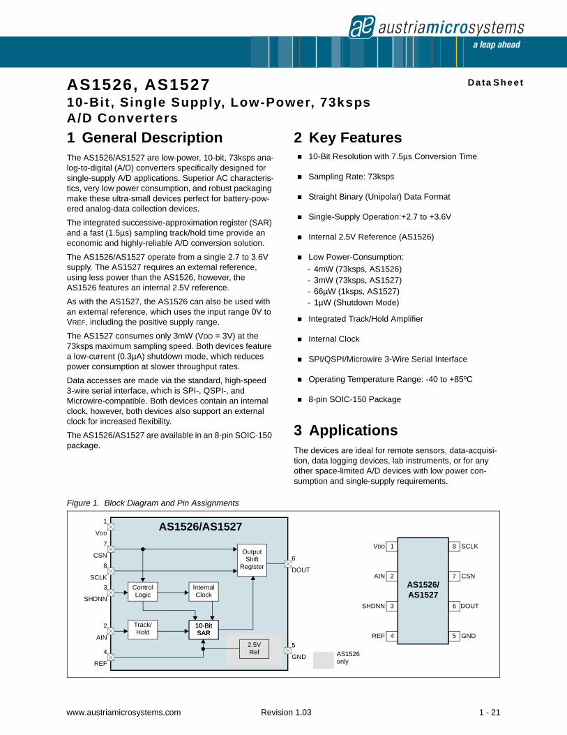
AS1526, AS1527 10-Bit , Single Supply, Low-Power, 73ksps A/D Converters
Data Sheet
1 General DescriptionThe AS1526/AS1527 are low-power, 10-bit, 73ksps ana-log-to-digital (A/D) converters specifically designed for single-supply A/D applications. Superior AC characteris-tics, very low power consumption, and robust packaging make these ultra-small devices perfect for battery-pow-ered analog-data collection devices.
The integrated successive-approximation register (SAR) and a fast (1.5µs) sampling track/hold time provide an economic and highly-reliable A/D conversion solution.
The AS1526/AS1527 operate from a single 2.7 to 3.6V supply. The AS1527 requires an external reference, using less power than the AS1526, however, the AS1526 features an internal 2.5V reference.
As with the AS1527, the AS1526 can also be used with an external reference, which uses the input range 0V to VREF, including the positive supply range.
The AS1527 consumes only 3mW (VDD = 3V) at the 73ksps maximum sampling speed. Both devices feature a low-current (0.3µA) shutdown mode, which reduces power consumption at slower throughput rates.
Data accesses are made via the standard, high-speed 3-wire serial interface, which is SPI-, QSPI-, and Microwire-compatible. Both devices contain an internal clock, however, both devices also support an external clock for increased flexibility.
The AS1526/AS1527 are available in an 8-pin SOIC-150 package.
Figure 1. Block Diagram and Pin Assignments
2 Key Features! 10-Bit Resolution with 7.5µs Conversion Time
! Sampling Rate: 73ksps
! Straight Binary (Unipolar) Data Format
! Single-Supply Operation:+2.7 to +3.6V
! Internal 2.5V Reference (AS1526)
! Low Power-Consumption: - 4mW (73ksps, AS1526)- 3mW (73ksps, AS1527)- 66µW (1ksps, AS1527)- 1µW (Shutdown Mode)
! Integrated Track/Hold Amplifier
! Internal Clock
! SPI/QSPI/Microwire 3-Wire Serial Interface
! Operating Temperature Range: -40 to +85ºC
! 8-pin SOIC-150 Package
3 ApplicationsThe devices are ideal for remote sensors, data-acquisi-tion, data logging devices, lab instruments, or for any other space-limited A/D devices with low power con-sumption and single-supply requirements.
AS1526/AS1527
ControlLogic
OutputShift
Register
InternalClock
10-BitSAR
Track/Hold
2.5VRef
AS1526/AS1527
4REF
AS1526 only
10-BitSAR
6
DOUT
5
GND
1
VDD
7
CSN8
SCLK3
SHDNN
2
AIN
4
REF
3SHDNN
2AIN
1VDD
5 GND
6 DOUT
7 CSN
8 SCLK
www.austriamicrosystems.com Revision 1.03 1 - 21
AS1526/AS1527Data Sheet
Contents1 General Description ..............................................................................................................................12 Key Features .........................................................................................................................................13 Applications ...........................................................................................................................................14 Pinout and Packaging ...........................................................................................................................3
Pin Assignments ...................................................................................................................................................3Pin Descriptions ....................................................................................................................................................3
5 Absolute Maximum Ratings ..................................................................................................................46 Electrical Characteristics .......................................................................................................................5
Timing Characteristics ..........................................................................................................................................77 Typical Operating Characteristics .........................................................................................................88 Detailed Description ............................................................................................................................ 11
Analog Input ........................................................................................................................................................11Input Protection ..............................................................................................................................................12
Track/Hold ...........................................................................................................................................................12External Clock .....................................................................................................................................................12Timing and Control ..............................................................................................................................................12Transfer Function ................................................................................................................................................14Reducing Supply Current ....................................................................................................................................14Internal 2.5V Reference (AS1526) ......................................................................................................................15External Reference .............................................................................................................................................15
9 Application Information .......................................................................................................................16Initialization .........................................................................................................................................................16Serial Interface ....................................................................................................................................................16
Serial Interface Configuration .........................................................................................................................16SPI and Microwire Interfaces .........................................................................................................................16QSPI 17
Layout Considerations ........................................................................................................................................18Package Drawings and Markings .......................................................................................................................19
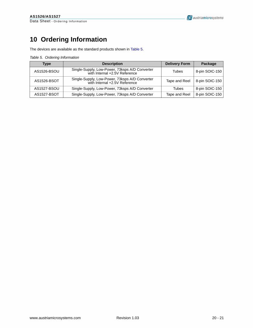
10 Ordering Information ........................................................................................................................20
www.austriamicrosystems.com Revision 1.03 2 - 21
AS1526/AS1527Data Sheet - P inou t and Packag ing
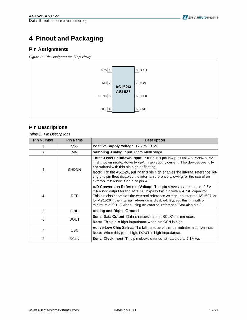
4 Pinout and PackagingPin AssignmentsFigure 2. Pin Assignments (Top View)
Pin DescriptionsTable 1. Pin Descriptions
Pin Number Pin Name Description1 VDD Positive Supply Voltage. +2.7 to +3.6V
2 AIN Sampling Analog Input. 0V to VREF range.
3 SHDNN
Three-Level Shutdown Input. Pulling this pin low puts the AS1526/AS1527 in shutdown mode, down to 4µA (max) supply current. The devices are fully operational with this pin high or floating. Note: For the AS1526, pulling this pin high enables the internal reference; let-ting this pin float disables the internal reference allowing for the use of an external reference. See also pin 4.
4 REF
A/D Conversion Reference Voltage. This pin serves as the internal 2.5V reference output for the AS1526; bypass this pin with a 4.7µF capacitor. This pin also serves as the external reference voltage input for the AS1527, or for AS1526 if the internal reference is disabled. Bypass this pin with a minimum of 0.1µF when using an external reference. See also pin 3.
5 GND Analog and Digital Ground
6 DOUTSerial Data Output. Data changes state at SCLK’s falling edge.Note: This pin is high-impedance when pin CSN is high.
7 CSNActive-Low Chip Select. The falling edge of this pin initiates a conversion.Note: When this pin is high, DOUT is high-impedance.
8 SCLK Serial Clock Input. This pin clocks data out at rates up to 2.1MHz.
AS1526/AS1527
4REF
3SHDNN
2AIN
1VDD
5 GND
6 DOUT
7 CSN
8 SCLK
www.austriamicrosystems.com Revision 1.03 3 - 21
AS1526/AS1527Data Sheet - Abso lu te Max imum Rat ings
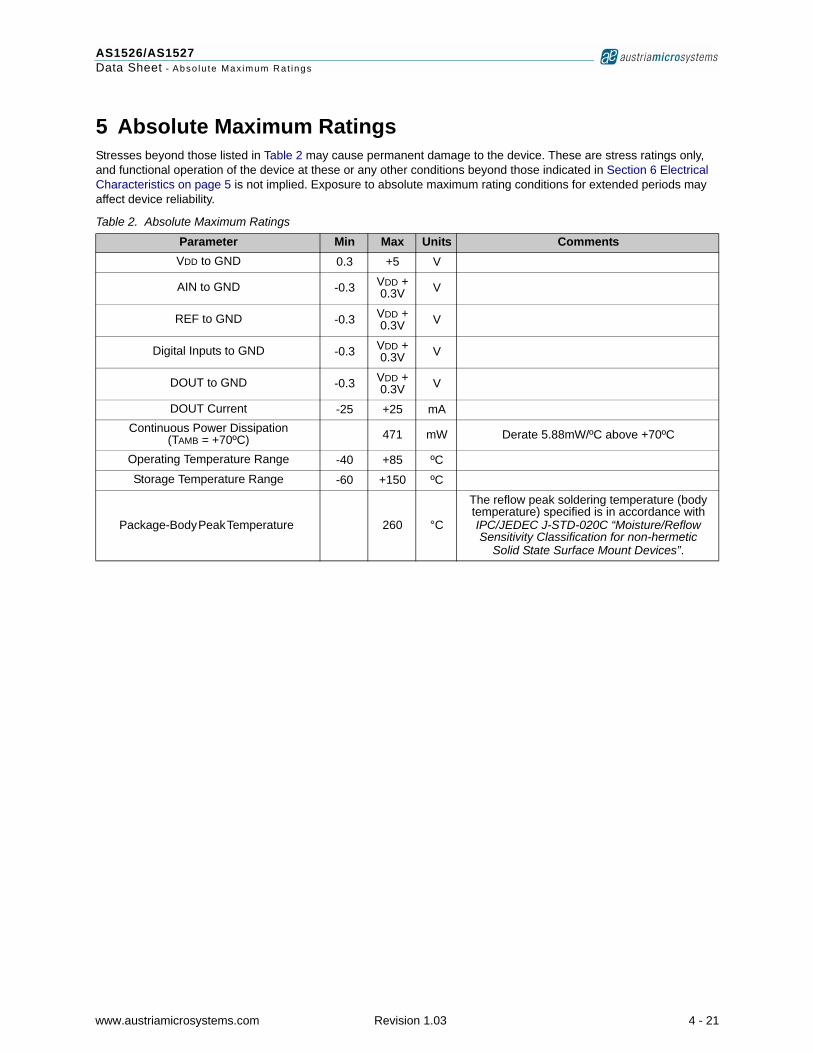
5 Absolute Maximum RatingsStresses beyond those listed in Table 2 may cause permanent damage to the device. These are stress ratings only, and functional operation of the device at these or any other conditions beyond those indicated in Section 6 Electrical Characteristics on page 5 is not implied. Exposure to absolute maximum rating conditions for extended periods may affect device reliability.
Table 2. Absolute Maximum Ratings
Parameter Min Max Units CommentsVDD to GND 0.3 +5 V
AIN to GND -0.3 VDD + 0.3V V
REF to GND -0.3 VDD + 0.3V V
Digital Inputs to GND -0.3 VDD + 0.3V V
DOUT to GND -0.3 VDD + 0.3V V
DOUT Current -25 +25 mAContinuous Power Dissipation
(TAMB = +70ºC) 471 mW Derate 5.88mW/ºC above +70ºC
Operating Temperature Range -40 +85 ºCStorage Temperature Range -60 +150 ºC
Package-Body Peak Temperature 260 °C
The reflow peak soldering temperature (body temperature) specified is in accordance withIPC/JEDEC J-STD-020C “Moisture/Reflow Sensitivity Classification for non-hermetic
Solid State Surface Mount Devices”.
www.austriamicrosystems.com Revision 1.03 4 - 21
AS1526/AS1527Data Sheet - E lec t r i ca l Charac te r i s t i cs
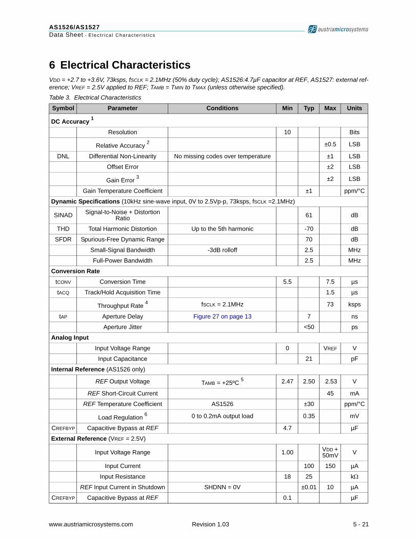
6 Electrical CharacteristicsVDD = +2.7 to +3.6V, 73ksps, fSCLK = 2.1MHz (50% duty cycle); AS1526:4.7µF capacitor at REF, AS1527: external ref-erence; VREF = 2.5V applied to REF; TAMB = TMIN to TMAX (unless otherwise specified).
Table 3. Electrical Characteristics
Symbol Parameter Conditions Min Typ Max Units
DC Accuracy 1
Resolution 10 Bits
Relative Accuracy 2 ±0.5 LSB
DNL Differential Non-Linearity No missing codes over temperature ±1 LSB
Offset Error ±2 LSB
Gain Error 3 ±2 LSB
Gain Temperature Coefficient ±1 ppm/°C
Dynamic Specifications (10kHz sine-wave input, 0V to 2.5Vp-p, 73ksps, fSCLK =2.1MHz)
SINAD Signal-to-Noise + Distortion Ratio 61 dB
THD Total Harmonic Distortion Up to the 5th harmonic -70 dB
SFDR Spurious-Free Dynamic Range 70 dB
Small-Signal Bandwidth -3dB rolloff 2.5 MHz
Full-Power Bandwidth 2.5 MHz
Conversion Rate tCONV Conversion Time 5.5 7.5 µs
tACQ Track/Hold Acquisition Time 1.5 µs
Throughput Rate 4 fSCLK = 2.1MHz 73 ksps
tAP Aperture Delay Figure 27 on page 13 7 ns
Aperture Jitter <50 ps
Analog Input Input Voltage Range 0 VREF V
Input Capacitance 21 pF
Internal Reference (AS1526 only)
REF Output Voltage TAMB = +25ºC 5 2.47 2.50 2.53 V
REF Short-Circuit Current 45 mA
REF Temperature Coefficient AS1526 ±30 ppm/°C
Load Regulation 6 0 to 0.2mA output load 0.35 mV
CREFBYP Capacitive Bypass at REF 4.7 µF
External Reference (VREF = 2.5V)
Input Voltage Range 1.00 VDD + 50mV V
Input Current 100 150 µA
Input Resistance 18 25 kΩ
REF Input Current in Shutdown SHDNN = 0V ±0.01 10 µA
CREFBYP Capacitive Bypass at REF 0.1 µF
www.austriamicrosystems.com Revision 1.03 5 - 21
AS1526/AS1527Data Sheet - E lec t r i ca l Charac te r i s t i cs
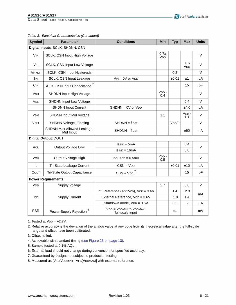
Digital Inputs: SCLK, SHDNN, CSN
VIH SCLK, CSN Input High Voltage 0.7x VDD V
VIL SCLK, CSN Input Low Voltage 0.3x VDD V
VHYST SCLK, CSN Input Hysteresis 0.2 V
IIN SCLK, CSN Input Leakage VIN = 0V or VDD ±0.01 ±1 µA
CIN SCLK, CSN Input Capacitance 7 15 pF
VSH SHDNN Input High Voltage VDD - 0.4 V
VSL SHDNN Input Low Voltage 0.4 V
SHDNN Input Current SHDNN = 0V or VDD ±4.0 µA
VSM SHDNN Input Mid Voltage 1.1 VDD - 1.1 V
VFLT SHDNN Voltage, Floating SHDNN = float VDD/2 V
SHDNN Max Allowed Leakage, Mid Input SHDNN = float ±50 nA
Digital Output: DOUT
VOL Output Voltage Low ISINK = 5mA 0.4
VISINK = 16mA 0.8
VOH Output Voltage High ISOURCE = 0.5mA VDD - 0.5 V
IL Tri-State Leakage Current CSN = VDD ±0.01 ±10 µA
COUT Tri-State Output Capacitance CSN = VDD 7 15 pF
Power Requirements VDD Supply Voltage 2.7 3.6 V
IDD Supply Current
Int. Reference (AS1526), VDD = 3.6V 1.4 2.0 mA
External Reference, VDD = 3.6V 1.0 1.4
Shutdown mode, VDD = 3.6V 0.3 2 µA
PSR Power-Supply Rejection 8VDD = VDDMIN to VDDMAX,
full-scale input ±1 mV
1. Tested at VDD = +2.7V. 2. Relative accuracy is the deviation of the analog value at any code from its theoretical value after the full-scale
range and offset have been calibrated. 3. Offset nulled.4. Achievable with standard timing (see Figure 25 on page 13).5. Sample tested at 0.1% AQL.6. External load should not change during conversion for specified accuracy.7. Guaranteed by design; not subject to production testing.8. Measured as [VFS(VDDMIN) - VFS(VDDMAX)] with external reference.
Table 3. Electrical Characteristics (Continued)
Symbol Parameter Conditions Min Typ Max Units
www.austriamicrosystems.com Revision 1.03 6 - 21
AS1526/AS1527Data Sheet - E lec t r i ca l Charac te r i s t i cs
Timing CharacteristicsVDD = +2.7 to +3.6V, TAMB = TMIN to TMAX (unless otherwise specified).
Figure 3. DOUT Enable-Time Load Circuits
Figure 4. DOUT Disable-Time Load Circuits
Table 4. Timing Characteristics
Parameter Symbol Conditions Min Typ Max Units
Acquisition Time 1
1. To guarantee acquisition time, tACQ is the maximum time the device takes to acquire the signal, and is also the minimum time needed for the signal to be acquired
tACQ 1.5 µs
SCLK Falling-to-DOUT Valid tDO Figure 3, CLOAD = 50pF 20 200 ns
CSN Falling-to-Output Enable tDV Figure 3, CLOAD = 50pF 240 ns
CSN Rising-to-Output Disable tTR Figure 4, CLOAD = 50pF 240 ns
SCLK Clock Frequency fSCLK 0 2.1 MHz
SCLK Pulse Width High tCH 200 ns
SCLK Pulse Width Low tCL 200 ns
SCLK Low-to-CSN Falling Setup Time tCS0 50 ns
DOUT Rising-to-SCLK Rising 2
2. Guaranteed by design; not subject to production testing.
tSTR 0 ns
CSN Pulse Width tCS 240 ns
CLOAD 50pF
CLOAD 50pF
6kΩ
GND
DGND
DOUT
DOUT
High-impedance to VOH and VOL to VOH
+2.7V
High-impedance to VOL and VOH to VOL
6kΩ
DGND
6kΩ CLOAD 50pF
CLOAD 50pF
6kΩ
DGND GND
DGND
DOUT
DOUT
VOH to high-impedance
+2.7V
VOL to high-impedance
www.austriamicrosystems.com Revision 1.03 7 - 21
AS1526/AS1527Data Sheet - Typ ica l Opera t ing Charac te r i s t i cs
7 Typical Operating CharacteristicsVDD = 3.0V, VREF = 2.5V, fSCLK = 2.1MHz, CLOAD = 50pF, TAMB = +25ºC (unless otherwise specified).Figure 5. Integral Nonlinearity vs. Digital Output Code Figure 6. Differential Nonlinearity vs. Digital Output Code
Figure 7. FFT @ 1kHz Figure 8. FFT @ 10kHz
Figure 9. ENOB vs. VREF Figure 10. ENOB vs. Input Signal Frequency
-1
-0.8
-0.6
-0.4
-0.2
0
0.2
0.4
0.6
0.8
1
0 256 512 768 1024Digital Output Code
INL
(LS
B)
.
-1
-0.8
-0.6
-0.4
-0.2
0
0.2
0.4
0.6
0.8
1
0 256 512 768 1024Digital Output Code
DN
L (L
SB
) .
-160
-140
-120
-100
-80
-60
-40
-20
0
0 10 20 30 40Input Signal Frequency (kHz)
FFT
(dB
C)
.
-160
-140
-120
-100
-80
-60
-40
-20
0
0 10 20 30 40Input Signal Frequency (kHz)
FFT
(dB
C)
.
Fsample = 80.8ksps NFFT = 16384
Fsample = 80.8ksps NFFT = 16384
9.77
9.8
9.83
9.86
9.89
9.92
9.95
0.8 1.2 1.6 2 2.4 2.8 3.2 3.6Reference Voltage (V)
EN
OB
(Bit)
.
9.89
9.9
9.91
9.92
9.93
9.94
9.95
0 10 20 30 40Frequency (kHz)
EN
OB
(Bit)
.
www.austriamicrosystems.com Revision 1.03 8 - 21
AS1526/AS1527Data Sheet - Typ ica l Opera t ing Charac te r i s t i cs
Figure 11. Supply Current vs. Supply Voltage Figure 12. Supply Current vs. Temperature
Figure 13. Shutdown Supply Current vs. Supply Voltage Figure 14. Shutdown Supply Current vs. Temperature
Figure 15. Offset Error vs. Supply Voltage Figure 16. Offset Voltage vs. Temperature
0
0.5
1
1.5
2
2.7 3 3.3 3.6Supply Voltage (V)
Sup
ply
Cur
rent
(mA
) .
0
0.5
1
1.5
2
-40 -15 10 35 60 85Temperature (°C)
Sup
ply
Cur
rent
(mA
) .
Internal Reference
External Reference
Internal Reference
External Reference
0
0.5
1
1.5
2
-40 -15 10 35 60 85Temperature (°C)
Sup
ply
Cur
rent
(µA
) .
0
0.25
0.5
0.75
1
2.7 3 3.3 3.6Supply Voltage (V)
Shu
tdow
n S
uppl
y C
urre
nt (µ
A)
.
0
0.1
0.2
0.3
0.4
0.5
-40 -15 10 35 60 85Temperature (°C)
Offs
et E
rror
(LS
B)
.
-0.2
-0.1
0
0.1
0.2
0.3
2.7 3 3.3 3.6Supply Voltage (V)
Offs
et E
rror
(LS
B)
.
www.austriamicrosystems.com Revision 1.03 9 - 21
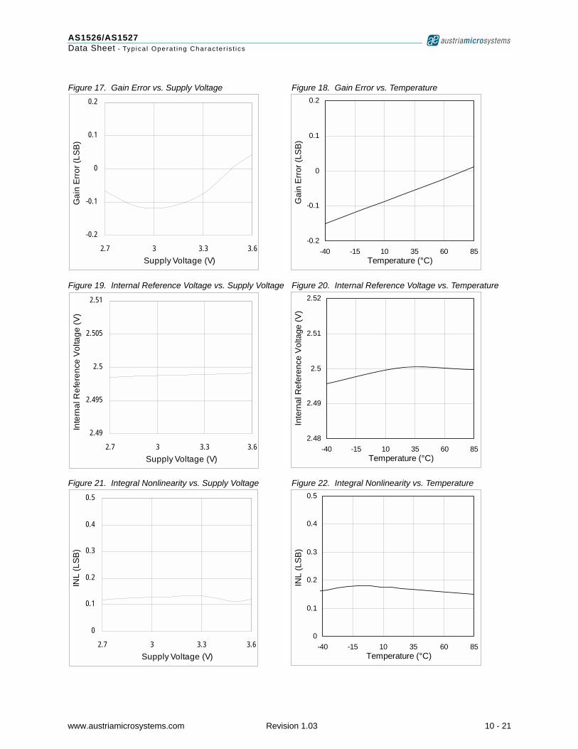
AS1526/AS1527Data Sheet - Typ ica l Opera t ing Charac te r i s t i cs
Figure 17. Gain Error vs. Supply Voltage Figure 18. Gain Error vs. Temperature
Figure 19. Internal Reference Voltage vs. Supply Voltage Figure 20. Internal Reference Voltage vs. Temperature
Figure 21. Integral Nonlinearity vs. Supply Voltage Figure 22. Integral Nonlinearity vs. Temperature
-0.2
-0.1
0
0.1
0.2
-40 -15 10 35 60 85Temperature (°C)
Gai
n E
rror (
LSB
) .
-0.2
-0.1
0
0.1
0.2
2.7 3 3.3 3.6Supply Voltage (V)
Gai
n Er
ror (
LSB
) .
2.48
2.49
2.5
2.51
2.52
-40 -15 10 35 60 85Temperature (°C)
Inte
rnal
Ref
eren
ce V
olta
ge (V
) .
2.49
2.495
2.5
2.505
2.51
2.7 3 3.3 3.6Supply Voltage (V)
Inte
rnal
Ref
eren
ce V
olta
ge (V
) .
0
0.1
0.2
0.3
0.4
0.5
-40 -15 10 35 60 85Temperature (°C)
INL
(LS
B)
.
0
0.1
0.2
0.3
0.4
0.5
2.7 3 3.3 3.6Supply Voltage (V)
INL
(LSB
) .
www.austriamicrosystems.com Revision 1.03 10 - 21

AS1526/AS1527Data Sheet - De ta i led Descr ip t ion
8 Detailed DescriptionThe AS1526/AS1527 analog-to-digital converters have two modes of operation:! Normal A/D Conversion Mode – Pulling pin SHDNN high or leaving it open puts the device into normal A/D conver-
sion mode.
! Shutdown Mode – Pulling pin SHDNN low shuts the device down and reduces supply current below 2µA (VDD ≤ 3.6V).
Note: Pulling pin CSN low starts a conversion. The conversion result is available at pin DOUT in unipolar serial for-mat (see Timing and Control on page 12).
Figure 23 shows a basic configuration for the AS1526/AS1527. The integrated input track/hold circuitry and a succes-sive-approximation register (SAR) circuitry convert analog input signals to a digital 10-bit output. No external-hold capacitor is needed for the track/hold circuit.
The devices convert analog input signals in the 0V to VREF range in 13µs (includes track/hold acquisition time).
The AS1526 internal reference is trimmed to 2.5V; the AS1527 requires an external reference. Both devices can accept external reference voltages from 1.0V to VDD. The serial interface requires only three digital lines (at pins SCLK, CSN, and DOUT) and provides a simple microprocessor interface.
Figure 23. Operational Diagram
Analog InputFigure 24 illustrates the integrated comparator sampling architecture. The full scale input voltage is set by the voltage at pin REF.
Figure 24. Equivalent Input Circuit
AS1526/AS1527
+2.7 to +3.6V
AS1526 – 4.7µFAS1527 – 0.1µF
Reference InputRequired for AS1527,
Optional for AS1526
0.1µF4.7µF+
6
DOUT
5
GND
1
VDD
7
CSN
8
SCLK
3
SHDNN
2
AIN
4
REF
+
–
+
ComparatorRIN
CSWITCH14pF
CHOLD13pF
–
REF
AIN
+
CHOLD13pF
–
SampleSwitch
CSWITCH includes all parasitics
GNDS&H and DAC
www.austriamicrosystems.com Revision 1.03 11 - 21
AS1526/AS1527Data Sheet - De ta i led Descr ip t ion
The devices’ input tracking circuitry has a 2.5MHz small-signal bandwidth, thus it is possible to under-sample (digitize high-speed transient events) and measure periodic signals with bandwidths exceeding the devices’ sampling rate.
Note: Anti-aliasing filtering should be used to avoid aliasing of unwanted high-frequency signals into the bandwidth of interest.
Input ProtectionInternal protection diodes clamp the analog input to VDD and GND, allowing the input to swing from (GND - 0.3V) to (VDD + 0.3V) without damage. However, for accurate conversions near full scale, the input must not exceed VDD by more than 50mV, or be lower than GND by 50mV.
Note: If the analog input exceeds the supply by 50mV, limit the input current to 2mA.
Track/HoldIn track mode, the analog signal is acquired and stored in the internal hold capacitors. During acquisition, the analog input at pin AIN charges capacitor CHOLD (see Figure 24 on page 11). Bringing CSN low ends the acquisition interval and the charge on CHOLD represent the sampled input voltage.
In hold mode, the T/H switches are opened thus the input is disconnected from the capacitor CHOLD. During this mode the successive approximation is performed which in turn forms a digital representation of the analog input signal. At the end of the conversion, the input side of the in meantime discharged CHOLD switches back to AIN, and CHOLD charges to the input signal again.
The maximum time for the T/H to acquire a signal (tACQ) is a function of how quickly its input capacitance is charged. tACQ increases proportionally to the input signal’s impedance, and at higher impedances more time must be allowed between conversions. tACQ is also the minimum time needed for the signal to be acquired, and is calculated by:
tACQ = 7(RS + RIN) x 21pF (EQ 1)Where:RIN = 4.5kΩRS = the input signal’s source impedance.tACQ is never less than 1.5µs. Source impedances < 1kΩ do not significantly affect the AC performance of the devices.
Note: Higher source impedances can be used if a 0.01µF capacitor is connected to the analog input. Note that the input capacitor forms an RC filter with the input source impedance, limiting the devices’ input signal bandwidth.
External ClockThe AS1526/AS1527 do not require an external clock for analog-to-digital data conversion. This allows the micropro-cessor to read back the conversion results at any clock rate from up to 2.1MHz at any time. The clock duty cycle is unrestricted if each clock phase is at least 200ns.
Note: The external clock must not be run while a conversion is in progress.
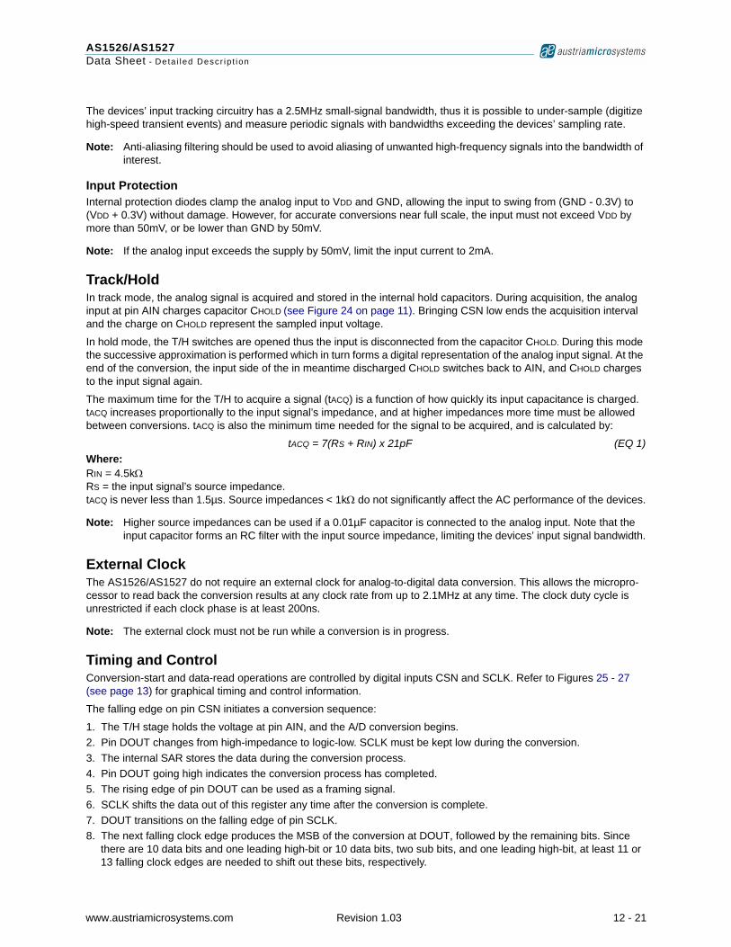
Timing and ControlConversion-start and data-read operations are controlled by digital inputs CSN and SCLK. Refer to Figures 25 - 27 (see page 13) for graphical timing and control information.
The falling edge on pin CSN initiates a conversion sequence:
1. The T/H stage holds the voltage at pin AIN, and the A/D conversion begins.2. Pin DOUT changes from high-impedance to logic-low. SCLK must be kept low during the conversion. 3. The internal SAR stores the data during the conversion process. 4. Pin DOUT going high indicates the conversion process has completed.5. The rising edge of pin DOUT can be used as a framing signal. 6. SCLK shifts the data out of this register any time after the conversion is complete. 7. DOUT transitions on the falling edge of pin SCLK. 8. The next falling clock edge produces the MSB of the conversion at DOUT, followed by the remaining bits. Since
there are 10 data bits and one leading high-bit or 10 data bits, two sub bits, and one leading high-bit, at least 11 or 13 falling clock edges are needed to shift out these bits, respectively.
www.austriamicrosystems.com Revision 1.03 12 - 21
AS1526/AS1527Data Sheet - De ta i led Descr ip t ion
9. Extra clock pulses occurring after the conversion result has been clocked out, and prior to a rising edge of CSN, produce trailing zeros at DOUT and have no effect on the conversion process.
10. For minimum cycle time, clock out the data with 10.5 clock cycles at full speed using the rising edge of DOUT as the EOC signal. Pull CSN high after reading the conversion’s LSB. After the specified minimum time (tCS) CSN can be pulled low to initiate the next conversion.
Figure 25. Serial Interface Standard Cycle Timing Diagram
Figure 26. Serial Interface Minimum Cycle Timing Diagram
Figure 27. Detailed Serial Interface Timing Diagram
CSN
SCLK
DOUT
ConversionIn Progress
Hold
EOC
Track/Hold Stage Track
Clock Out Serial Data
Track
Cycle TimeTotal = 13.7µs
Trailing0s Idle
0.24µstCS0µstCONV
7.5µs
Hold
Interface Idle
B9 B8 B7 B6 B5 B4 B3 B2 B1 B0 S1 S0
0µs 12.5 x 0.476µs = 5.95µs
SubBits
HoldTrack/Hold Stage Track Track Hold
Total = 12.74µsCycle Time
DOUT B9 B8 B7 B6 B5 B4 B3 B1 B0
CSN
EOC Clock Out Serial Data IdleInterface Idle
0.24µstCS
7.5µstCONV 0µs 10.5 x 0.476µs = 5µs
SCLK
B2
ConversionIn Progress
Track/Acquire
CSN
SCLK
DOUT
Internal Track/Hold
tCONV
tAP
tDV
tSTRHold
tCSO
tDO
tCH
tCL
tCS
tTR
Track/Acquire
B0 S1 S0
www.austriamicrosystems.com Revision 1.03 13 - 21
AS1526/AS1527Data Sheet - De ta i led Descr ip t ion
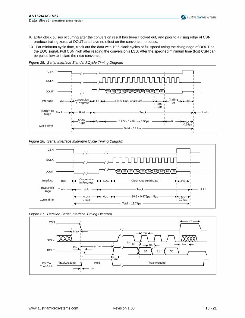
Transfer Function The data output from the AS1526/AS1527 is binary (unipolar), and Figure 28 depicts the nominal transfer function. Code transitions occur midway between successive integer LSB values.
Note: If VREF = +2.50V, then 1 LSB = 2.44mV (2.50V/1024).
Figure 28. Unipolar Transfer Function
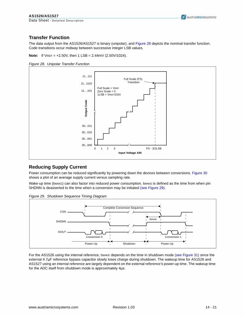
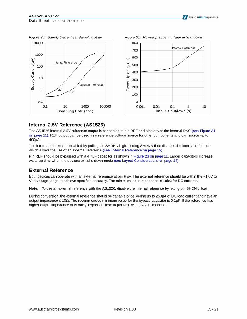
Reducing Supply CurrentPower consumption can be reduced significantly by powering down the devices between conversions. Figure 30 shows a plot of an average supply current versus sampling rate.
Wake-up time (tWAKE) can also factor into reduced power consumption. tWAKE is defined as the time from when pin SHDNN is deasserted to the time when a conversion may be initiated (see Figure 29).
Figure 29. Shutdown Sequence Timing Diagram
For the AS1526 using the internal reference, tWAKE depends on the time in shutdown mode (see Figure 31) since the external 4.7µF reference bypass capacitor slowly loses charge during shutdown. The wakeup time for AS1526 and AS1527 using an internal reference are largely dependent on the external reference’s power-up time. The wakeup time for the ADC itself from shutdown mode is approximately 4µs.
11...111
11...1110
11....101
00...011
00...010
00...001
00...000
Out
put C
ode
0 1 2 3Input Voltage AIN
FS - 3/2LSB
Full Scale (FS) Transition
Full Scale = VREFZero Scale = 01LSB = VREF/1024
Complete Conversion Sequence
Conversion 0 Conversion 1
Power-Up Shutdown
tWAKE
Power-Up
CSN
SHDNN
DOUT
www.austriamicrosystems.com Revision 1.03 14 - 21
AS1526/AS1527Data Sheet - De ta i led Descr ip t ion
Figure 30. Supply Current vs. Sampling Rate Figure 31. Powerup Time vs. Time in Shutdown
Internal 2.5V Reference (AS1526)The AS1526 internal 2.5V reference output is connected to pin REF and also drives the internal DAC (see Figure 24 on page 11). REF output can be used as a reference voltage source for other components and can source up to 400µA.
The internal reference is enabled by pulling pin SHDNN high. Letting SHDNN float disables the internal reference, which allows the use of an external reference (see External Reference on page 15).
Pin REF should be bypassed with a 4.7µF capacitor as shown in Figure 23 on page 11. Larger capacitors increase wake-up time when the devices exit shutdown mode (see Layout Considerations on page 18)
External Reference Both devices can operate with an external reference at pin REF. The external reference should be within the +1.0V to VDD voltage range to achieve specified accuracy. The minimum input impedance is 18kΩ for DC currents.
Note: To use an external reference with the AS1526, disable the internal reference by letting pin SHDNN float.
During conversion, the external reference should be capable of delivering up to 250µA of DC load current and have an output impedance ≤ 10Ω. The recommended minimum value for the bypass capacitor is 0.1µF. If the reference has higher output impedance or is noisy, bypass it close to pin REF with a 4.7µF capacitor.
0.1
1
10
100
1000
10000
0.1 10 1000 100000Sampling Rate (sps)
Supp
ly C
urre
nt (µ
A)
.
0
100
200
300
400
500
600
700
800
0.001 0.01 0.1 1 10Tim e in Shutdown (s )
Pow
er-U
p de
lay
(µs)
.
Internal Reference
External Reference
3V3V
Internal Reference
www.austriamicrosystems.com Revision 1.03 15 - 21
AS1526/AS1527Data Sheet - App l ica t ion In fo rmat ion
9 Application InformationInitialization When power is first applied, and if SHDNN is not pulled low, it takes the fully discharged 4.7µF reference bypass capacitor up to 20ms to provide adequate charge for specified accuracy.
With an external reference, the initialization time is 10µs after the power supplies have stabilized.
Note: A/D conversions must not be started during initialization of the AS1526/AS1527.
Serial InterfaceThe AS1526/AS1527 fully support SPI, QSPI, and Microwire interfaces. For SPI, select the correct clock polarity and sampling edge in the SPI control registers (set CPOL = 0 and CPHA = 0).
Microwire, SPI, and QSPI all transmit a byte and receive a byte at the same time.
Serial Interface Configuration The AS1526/AS1527 serial interface can be configured with the following procedure:
1. Put the microprocessor’s serial interface into master mode (so that it generates the serial clock). 2. Select a clock frequency up to 2.1MHz. 3. Keeping SCLK low, pull CSN low via one of the microprocessor’s general-purpose I/O lines. 4. Monitor DOUT for its rising edge to determine the EOC, or wait the maximum conversion time specified before acti-
vating SCLK.5. Activate SCLK for a minimum of 11 clock cycles. The first falling clock edge produces the MSB of the conversion.
Output data transitions on the falling edge of SCLK, and is available in MSB-first format at pin DOUT. Observe the SCLK to DOUT valid timing characteristic. Data can be clocked into the microprocessor on the rising edge of SCLK.
6. CSN should be pulled high at or after the 13th falling clock edge. If CSN remains low, trailing zeros are clocked out after the LSB.
7. With CSN = high, wait the minimum specified time, tCS, before initiating a new conversion by pulling CSN low. If a conversion is aborted by pulling CSN high before the conversion’s end, wait for the minimum acquisition time, tACQ, before starting a new conversion.
Note: CSN must be held low until all data bits are clocked out. 8. Data can be output in two bytes or continuously (see Figure 34 on page 17). The bytes contain the result of the con-
version padded with one leading 1, two sub-bits, and trailing 0s.
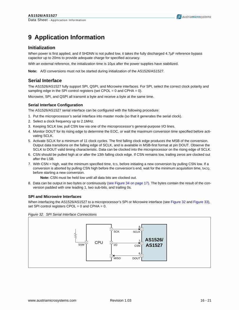
SPI and Microwire InterfacesWhen interfacing the AS1526/AS1527 to a microprocessor’s SPI or Microwire interface (see Figure 32 and Figure 33), set SPI control registers CPOL = 0 and CPHA = 0.
Figure 32. SPI Serial Interface Connections
AS1526/AS1527CPUSSM
MISO
I/O
SCK
6
DOUT
7
CSN
8
SCLK
www.austriamicrosystems.com Revision 1.03 16 - 21
AS1526/AS1527Data Sheet - App l ica t ion In fo rmat ion
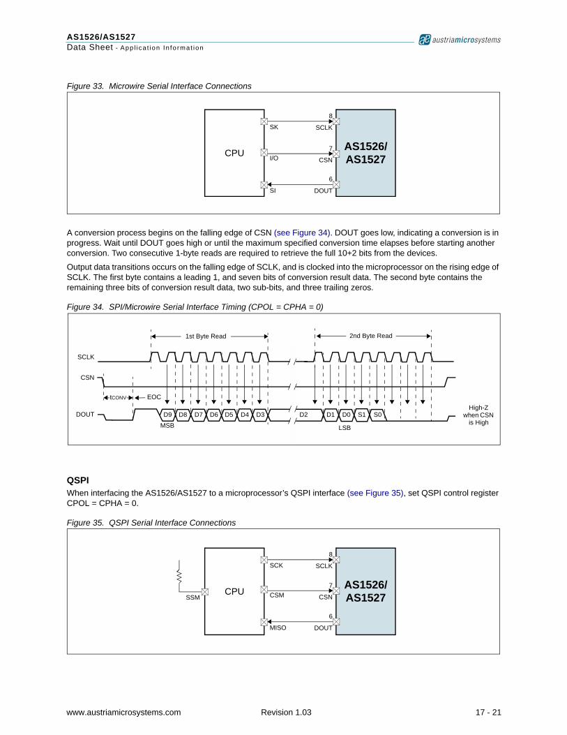
Figure 33. Microwire Serial Interface Connections
A conversion process begins on the falling edge of CSN (see Figure 34). DOUT goes low, indicating a conversion is in progress. Wait until DOUT goes high or until the maximum specified conversion time elapses before starting another conversion. Two consecutive 1-byte reads are required to retrieve the full 10+2 bits from the devices.
Output data transitions occurs on the falling edge of SCLK, and is clocked into the microprocessor on the rising edge of SCLK. The first byte contains a leading 1, and seven bits of conversion result data. The second byte contains the remaining three bits of conversion result data, two sub-bits, and three trailing zeros.
Figure 34. SPI/Microwire Serial Interface Timing (CPOL = CPHA = 0)
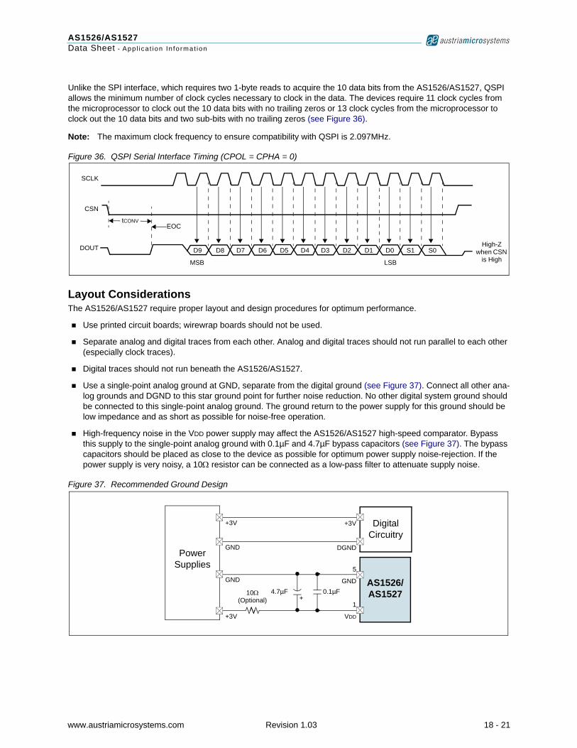
QSPIWhen interfacing the AS1526/AS1527 to a microprocessor’s QSPI interface (see Figure 35), set QSPI control register CPOL = CPHA = 0.
Figure 35. QSPI Serial Interface Connections
AS1526/AS1527CPU
SI
I/O
SK
6
DOUT
7
CSN
8
SCLK
1st Byte Read 2nd Byte Read
LSBMSB
EOCtCONV
CSN
SCLK
DOUT D9 D8 D7 D6 D5 D4 D3 D2 D1 D0 S1 S0High-Z
when CSN is High
AS1526/AS1527CPU
SSM
MISO
CSM
SCK
6
DOUT
7
CSN
8
SCLK
www.austriamicrosystems.com Revision 1.03 17 - 21
AS1526/AS1527Data Sheet - App l ica t ion In fo rmat ion
Unlike the SPI interface, which requires two 1-byte reads to acquire the 10 data bits from the AS1526/AS1527, QSPI allows the minimum number of clock cycles necessary to clock in the data. The devices require 11 clock cycles from the microprocessor to clock out the 10 data bits with no trailing zeros or 13 clock cycles from the microprocessor to clock out the 10 data bits and two sub-bits with no trailing zeros (see Figure 36).
Note: The maximum clock frequency to ensure compatibility with QSPI is 2.097MHz.
Figure 36. QSPI Serial Interface Timing (CPOL = CPHA = 0)
Layout ConsiderationsThe AS1526/AS1527 require proper layout and design procedures for optimum performance.
! Use printed circuit boards; wirewrap boards should not be used.
! Separate analog and digital traces from each other. Analog and digital traces should not run parallel to each other (especially clock traces).
! Digital traces should not run beneath the AS1526/AS1527.
! Use a single-point analog ground at GND, separate from the digital ground (see Figure 37). Connect all other ana-log grounds and DGND to this star ground point for further noise reduction. No other digital system ground should be connected to this single-point analog ground. The ground return to the power supply for this ground should be low impedance and as short as possible for noise-free operation.
! High-frequency noise in the VDD power supply may affect the AS1526/AS1527 high-speed comparator. Bypass this supply to the single-point analog ground with 0.1µF and 4.7µF bypass capacitors (see Figure 37). The bypass capacitors should be placed as close to the device as possible for optimum power supply noise-rejection. If the power supply is very noisy, a 10Ω resistor can be connected as a low-pass filter to attenuate supply noise.
Figure 37. Recommended Ground Design
SCLK
CSN
DOUT
EOCtCONV
LSBMSB
D9 D8 D7 D6 D5 D4 D3 D2 D1 D0 S1 S0High-Z
when CSN is High
AS1526/AS1527
Power Supplies
DigitalCircuitry
0.1µF+
4.7µF10Ω(Optional)
GND
GND
+3V
1
VDD
5
GND
+3V
+3V
DGND
www.austriamicrosystems.com Revision 1.03 18 - 21
AS1526/AS1527Data Sheet - App l ica t ion In fo rmat ion
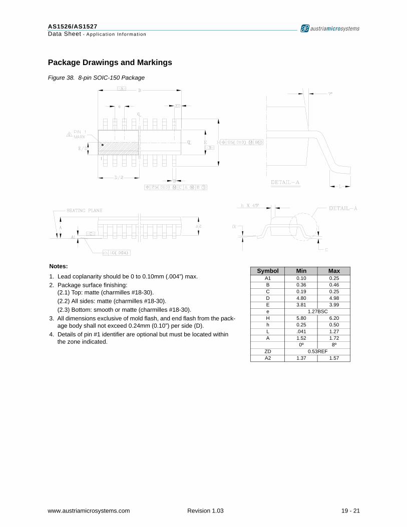
Package Drawings and Markings
Figure 38. 8-pin SOIC-150 Package
Symbol Min MaxA1 0.10 0.25B 0.36 0.46C 0.19 0.25D 4.80 4.98E 3.81 3.99e 1.27BSCH 5.80 6.20h 0.25 0.50L .041 1.27A 1.52 1.72
0º 8ºZD 0.53REFA2 1.37 1.57
Notes:1. Lead coplanarity should be 0 to 0.10mm (.004”) max. 2. Package surface finishing:
(2.1) Top: matte (charmilles #18-30).(2.2) All sides: matte (charmilles #18-30).(2.3) Bottom: smooth or matte (charmilles #18-30).
3. All dimensions exclusive of mold flash, and end flash from the pack-age body shall not exceed 0.24mm (0.10”) per side (D).
4. Details of pin #1 identifier are optional but must be located within the zone indicated.
www.austriamicrosystems.com Revision 1.03 19 - 21
AS1526/AS1527Data Sheet - Order ing In format ion
10 Ordering InformationThe devices are available as the standard products shown in Table 5.
Table 5. Ordering Information
Type Description Delivery Form Package
AS1526-BSOU Single-Supply, Low-Power, 73ksps A/D Converter with Internal +2.5V Reference Tubes 8-pin SOIC-150
AS1526-BSOT Single-Supply, Low-Power, 73ksps A/D Converter with Internal +2.5V Reference Tape and Reel 8-pin SOIC-150
AS1527-BSOU Single-Supply, Low-Power, 73ksps A/D Converter Tubes 8-pin SOIC-150AS1527-BSOT Single-Supply, Low-Power, 73ksps A/D Converter Tape and Reel 8-pin SOIC-150
www.austriamicrosystems.com Revision 1.03 20 - 21
AS1526/AS1527Data Sheet
CopyrightsCopyright © 1997-2007, austriamicrosystems AG, Schloss Premstaetten, 8141 Unterpremstaetten, Austria-Europe. Trademarks Registered ®. All rights reserved. The material herein may not be reproduced, adapted, merged, trans-lated, stored, or used without the prior written consent of the copyright owner.
All products and companies mentioned are trademarks or registered trademarks of their respective companies.
DisclaimerDevices sold by austriamicrosystems AG are covered by the warranty and patent indemnification provisions appearing in its Term of Sale. austriamicrosystems AG makes no warranty, express, statutory, implied, or by description regarding the information set forth herein or regarding the freedom of the described devices from patent infringement. austriami-crosystems AG reserves the right to change specifications and prices at any time and without notice. Therefore, prior to designing this product into a system, it is necessary to check with austriamicrosystems AG for current information. This product is intended for use in normal commercial applications. Applications requiring extended temperature range, unusual environmental requirements, or high reliability applications, such as military, medical life-support or life-sustaining equipment are specifically not recommended without additional processing by austriamicrosystems AG for each application. For shipments of less than 100 parts the manufacturing flow might show deviations from the standard production flow, such as test flow or test location.
The information furnished here by austriamicrosystems AG is believed to be correct and accurate. However, austriamicrosystems AG shall not be liable to recipient or any third party for any damages, including but not limited to personal injury, property damage, loss of profits, loss of use, interruption of business or indirect, special, incidental or consequential damages, of any kind, in connection with or arising out of the furnishing, performance or use of the tech-nical data herein. No obligation or liability to recipient or any third party shall arise or flow out of austriamicrosystems AG rendering of technical or other services.
Contact InformationHeadquartersaustriamicrosystems AGA-8141 Schloss Premstaetten, Austria
Tel: +43 (0) 3136 500 0Fax: +43 (0) 3136 525 01
For Sales Offices, Distributors and Representatives, please visit:
http://www.austriamicrosystems.com/contact
www.austriamicrosystems.com Revision 1.03 21 - 21
![tbd - Digi-Key Sheets/Austriamicrosystems PDFs/AS7261_V1-00_2016...ams Datasheet Page 5 [v1-00] 2016-Dec-30 Document Feedback AS7261 − Absolute Maximum Ratings Stresses beyond those](https://img.pdfslide.net/doc/110x75/5e53c6b8ade47a26b947ad37/tbd-digi-key-sheetsaustriamicrosystems-pdfsas7261v1-002016-ams-datasheet.jpg)


![AS399x UHF Pico Reader - Digi-Key Notes/austriamicrosystems... · [v1-00] 2014-Jul-24 Document Feedback AS399x UHF Pico Reader ... o Between the Controller and the AS399x is SPI via](https://img.pdfslide.net/doc/110x75/5b5286237f8b9af4408da77f/as399x-uhf-pico-reader-digi-key-notesaustriamicrosystems-v1-00-2014-jul-24.jpg)