Embed Size (px)
Citation preview
Reference: CMV2000-datasheet-v2.13
CMV2000 v2 Datasheet Page 1 of 63
© 2014 CMOSIS bvba
2.2 Megapixel machine vision CMOS image sensor
Datasheet

Reference: CMV2000-datasheet-v2.13
CMV2000 v2 Datasheet Page 2 of 63
© 2014 CMOSIS bvba
Change record
Issue Date Modification
1 06/05/2009 Origination
1.1 12/11/2009 - Corrected register address of sub_s[7:0] to ‘35’ (p 29/30/33)
1.2 11/01/2010 Adjusted min input frequency (chapter 3.5)
1.3 14/01/2010 Adjusted pin width in package drawing
2.7 29/03/2010 Added spectral response
Added spectral response for color devices
Updated specifications for version 2 devices
Changed VDD18 to VDD20
Added ordering info
Added handling and soldering procedures
Removed “confidential” from footer
Added recommended and adjustable register settings
2.1 22/7/2010 Frame rate calculation included
2.2 2/8/2010 Read-out in 12 bit mode added
2.3 1/9/2010 Added exposure time offset ((0.65 x register73 x clk_per x 129)
2.4 17/9/2010 Added Vtf_l1 to GND remark
2.5 19/10/2010 Added E12 spectral response curve and part numbers
2.6 11/1/2011 Added RGB Bayer pattern details
2.7 1/2/2011 Added electrical IO specifications
2.8 25/3/2011 Updated reflow soldering profile
2.9 13/4/2011 Changed tilt to 0.2 degrees, updated spectral response, changed exposure time
formula
2.9.1 20/5/2011 Changed 12 bit read-out mode (removed 16 and 8 outputs)
2.9.2 17/11/2011 Add frame rate calculation and examples
2.9.3 24/02/2012 Added:
- Temperature sensor details
- Image flipping details
- Power consumption details
- Gain details
- LCC package
Full revision
2.9.4 23/03/2012 Added:
- Input clocks phase
- LVDS termination
- LVDS TIA/EIA-644A standard
- Details on frame rate in external mode
- Use of register 125
- Minimum length of SYS_RES_N and FRAME_REQ
- Dark current doubling rate
- Offset details
- LCC pinout list
- Pin layout
Changed FOT_REG_VALUE to reg73
Layout changes

Reference: CMV2000-datasheet-v2.13
CMV2000 v2 Datasheet Page 3 of 63
© 2014 CMOSIS bvba
Issue Date Modification
2.9.5 24/05/2012 Added:
- Self-heating
- Supply peaks and decoupling
- I/O capacitance
- Power supplies startup sequence
- Overview outputs vs. channel mapping
- Actual gain vs. register setting for multiple clock speeds
- Typical response curve
Updated package drawing PGA dim. 8.889 to 0.889
2.9.6 30/07/2012 Added:
- PLR Vlow2/3 enable bit
- Sampling of digital inputs on rising CLK_IN
- Details on LVDS data out in multiplex modes
- CTR channel bits on TDIG1 and TDIG2 pins
- Evaluation kit available
- Minimum time between Frane_
- req pulses in internal mode
- Temperature sensor calibration example
Updated:
- Bayer pattern figure (pixel(0,0) green red). No actual device change
compared to previous devices.
- Supply noise influence
- Control bit INTE1/2 (no FOT overlap)
- FOT and Read-out time rounding
- Detailed timing of control channel figure
- LVDS clock delay figure (CLK_IN period)
- SPI timing from SPI upload to FRAME_REQ (1µs 1ms)
Removed:
- Reference errors
2.9.7 01/08/2013 Added:
- Pin head dimensions to package drawing
- TDIG1 and TDIG2 addresses to register overview
- Recommended FOT register settings to register overview
- Angular response curve
- Minimum exposure value
Updated:
- Training pattern of control channel
- Text and figure in Image flipping chapter
- Text and figure in Color Filter chapter
- Assembly drawing: now refers to pixel(0,0), added dimensions, transparent
view, pin numbers and corrected tile of die
- Supply settings table: peak current calculation, typical values to
recommended values, supply voltage range
- Connection diagram: changed 1.8V to 2.1V
- Response curve: replaced figure
- Temperature sensor figure now refers to pixel (0,0)
- Start-up sequence: time after SPI upload described more accurately
- LVDS driver specification: Voc dependency

Reference: CMV2000-datasheet-v2.13
CMV2000 v2 Datasheet Page 4 of 63
© 2014 CMOSIS bvba
Issue Date Modification
2.10 04/12/2013 Added:
- Skew limits for LVDS clock
Updated:
- Added settling time to reset sequence figure
- Corrected some spelling mistakes
- Some layout improvements
- Assembly drawing: corrected pixel(0,0) location
- Mechanical drawing: now has correct dimensions for cavity, and higher
resolution
- Recommended register settings table is now sorted on register address.
- Corrected aspect ratio for figure 29
- Temperature sensor location figure is updated
2.11 20/03/2014 Added:
- The FOT register can be lowered to 5, when required for very short
integration times
- The pin list description now lists what pins are optional
- Recommendation for unused pin in pinning chapter
- Description for i_lvds register. Lowering this can be useful for meeting EMC
standards
- All necessary register names are now in the register overview
- All register addresses in Chapter 5 now include bit numbers
- Part numbers for all package types are now included in the Ordering
Information table
Updated:
- Register overview: some new descriptions and references
- New figures for transmittance and QE are easier to read
- “color” register is now named “mono”, to better fit the description
- Pin list table is now sorted on function rather than pin number
- Specification overview in Chapter 1.3 is now clearer
- Description for optimizing register settings is now more complete
- Description for start-up and reset sequence
- Vtglow2 and Vtglow3 registers are 6 bits long, instead of 7
- Description for settling time should be clearer now
- LCC package was listed as 95 pins in the spec overview, should be 92 pins
Removed:
- Pixel coordinates on block diagram are removed as they were causing
confusion
2.12 28/01/2015 Updated:
- The power figure in the Specification Overview is now more accurate; it
considers the sensor configuration
- The exposure time is shortest in external exposure mode, so this mode is
added to the calculation.
- FRAME_REQ is level sensitive, not edge sensitive
- Maximum number of frames is 65535, not 65548
- Corrected note that said that the exposure starts directly after F_REQ, there
is a delay between the two
- Corrected calibration procedure, step 2 should be repeated, not step 1.
Removed
- Nr_slopes2 register from overview, this is an unused register.
- Scratch/dig/bubble spec for cover glass

Reference: CMV2000-datasheet-v2.13
CMV2000 v2 Datasheet Page 5 of 63
© 2014 CMOSIS bvba
Issue Date Modification
2.13 18/06/2015 Updated:
- LCC pin layout now correctly says it’s the bottom view, not the top
- LCC Product number now for AR coated glass only
Added
- Transmittance curve for AR coated glass
Disclaimer
CMOSIS reserves the right to change the product, specification and other information contained in this document without notice. Although CMOSIS does its best efforts to provide correct information, this is not warranted.
Reference: CMV2000-datasheet-v2.13
CMV2000 v2 Datasheet Page 6 of 63
© 2014 CMOSIS bvba
Table of Contents
1 Introduction ........................................................................................................................................................... 9
1.1 Overview ....................................................................................................................................................................... 9
1.2 Features ........................................................................................................................................................................ 9
1.3 Specifications ................................................................................................................................................................ 9
1.4 Connection diagram ................................................................................................................................................... 10
2 Sensor architecture .............................................................................................................................................. 11
2.1 Pixel array.................................................................................................................................................................... 11
2.2 Analog front end ......................................................................................................................................................... 12
2.3 LVDS block ................................................................................................................................................................... 12
2.4 Sequencer ................................................................................................................................................................... 12
2.5 SPI interface ................................................................................................................................................................ 12
2.6 Temperature sensor ................................................................................................................................................... 12
3 Driving the CMV2000 ........................................................................................................................................... 14
Supply settings ............................................................................................................................................................ 14
3.1 14
3.2 Biasing ......................................................................................................................................................................... 14
3.3 Digital input pins ......................................................................................................................................................... 14
3.4 Electrical IO specifications ......................................................................................................................................... 15
3.4.1 Digital I/O CMOS/TTL DC specifications (see pin list for specific pins) ....................................................... 15
3.4.2 TIA/EIA-644A LVDS driver specifications (OUTx_N/P, OUTCLK_N/P, OUTCTR_N/P) ................................ 15
3.4.3 TIA/EIA-644A LVDS receiver specifications (LVDS_CLK_N/P) ...................................................................... 15
3.5 Input clock ................................................................................................................................................................... 16
3.6 Frame rate calculation ............................................................................................................................................... 17
3.7 Start-up sequence ...................................................................................................................................................... 18
3.8 Reset sequence ........................................................................................................................................................... 19
3.9 SPI programming ........................................................................................................................................................ 19
3.9.1 SPI write .......................................................................................................................................................... 19
3.9.2 SPI read ............................................................................................................................................................ 20
3.10 Requesting a frame .................................................................................................................................................... 20
3.10.1 Internal exposure control .............................................................................................................................. 21
3.10.2 External exposure time .................................................................................................................................. 22
4 Reading out the sensor ........................................................................................................................................ 23
4.1 LVDS data outputs ...................................................................................................................................................... 23
4.2 Low-level pixel timing ................................................................................................................................................ 23

Reference: CMV2000-datasheet-v2.13
CMV2000 v2 Datasheet Page 7 of 63
© 2014 CMOSIS bvba
4.3 Read-out timing .......................................................................................................................................................... 24
4.3.1 10 Bit mode ..................................................................................................................................................... 24
4.3.2 12 Bit mode ..................................................................................................................................................... 25
4.4 Pixel remapping .......................................................................................................................................................... 25
4.4.1 16 Outputs ...................................................................................................................................................... 25
4.4.2 8 Outputs......................................................................................................................................................... 26
4.4.3 4 Outputs......................................................................................................................................................... 26
4.4.4 2 Outputs......................................................................................................................................................... 26
4.4.5 Overview ......................................................................................................................................................... 27
4.5 Control channel .......................................................................................................................................................... 27
4.5.1 DVAL, LVAL, FVAL............................................................................................................................................ 28
4.6 Training data ............................................................................................................................................................... 29
5 Image sensor programming .................................................................................................................................. 30
5.1 Exposure modes ......................................................................................................................................................... 30
5.2 High dynamic range modes ....................................................................................................................................... 30
5.2.1 Interleaved read-out ...................................................................................................................................... 31
5.2.2 Piecewise linear response .............................................................................................................................. 32
5.2.3 Multi-frame read-out ..................................................................................................................................... 34
5.3 Windowing .................................................................................................................................................................. 35
5.3.1 Single window ................................................................................................................................................. 35
5.3.2 Multiple windows ........................................................................................................................................... 35
5.4 Image flipping ............................................................................................................................................................. 37
5.5 Image subsampling ..................................................................................................................................................... 37
5.5.1 Simple subsampling ........................................................................................................................................ 37
5.5.2 Advanced subsampling .................................................................................................................................. 38
5.6 Number of frames ...................................................................................................................................................... 39
5.7 Output mode .............................................................................................................................................................. 39
5.8 Training pattern .......................................................................................................................................................... 39
5.9 10-bit or 12-bit mode ................................................................................................................................................. 39
5.10 Data rate ..................................................................................................................................................................... 39
5.11 Power control ............................................................................................................................................................. 40
5.12 Offset and gain ........................................................................................................................................................... 40
5.12.1 Offset ............................................................................................................................................................... 40
5.12.2 Gain .................................................................................................................................................................. 41
5.13 Recommended register settings ............................................................................................................................... 42
5.13.1 Adjusting registers for optimal performance ............................................................................................... 42
6 Register overview ................................................................................................................................................ 43

Reference: CMV2000-datasheet-v2.13
CMV2000 v2 Datasheet Page 8 of 63
© 2014 CMOSIS bvba
7 Mechanical specifications .................................................................................................................................... 46
7.1 Package drawing ......................................................................................................................................................... 46
7.1.1 95 pins µPGA and LGA .................................................................................................................................... 46
7.1.2 92 pins LCC ...................................................................................................................................................... 47
7.2 Assembly drawing ...................................................................................................................................................... 48
7.3 Cover glass .................................................................................................................................................................. 49
7.4 Color filters ................................................................................................................................................................. 49
8 Response curve .................................................................................................................................................... 51
9 Spectral response ................................................................................................................................................. 52
9.1 5µm epi devices .......................................................................................................................................................... 52
9.2 12µm epi devices ........................................................................................................................................................ 52
10 Angular response ................................................................................................................................................. 53
11 Pinning ................................................................................................................................................................. 54
11.1 Pin list .......................................................................................................................................................................... 54
11.2 µPGA and LGA pin layout ........................................................................................................................................... 56
11.3 LCC pin layout ............................................................................................................................................................. 56
12 Specification overview ......................................................................................................................................... 57
13 Ordering info ........................................................................................................................................................ 59
14 Handling and soldering procedure ....................................................................................................................... 60
14.1 Soldering ..................................................................................................................................................................... 60
14.1.1 Manual soldering ............................................................................................................................................ 60
14.1.2 Wave soldering ............................................................................................................................................... 60
14.1.3 Reflow soldering ............................................................................................................................................. 61
14.1.4 Soldering recommendations.......................................................................................................................... 61
14.2 Handling image sensors ............................................................................................................................................. 61
14.2.1 ESD ................................................................................................................................................................... 61
14.2.2 Glass cleaning ................................................................................................................................................. 61
14.2.3 Image sensor storing ...................................................................................................................................... 61
15 Evaluation kit ....................................................................................................................................................... 62
16 Additional information ......................................................................................................................................... 63

Reference: CMV2000-datasheet-v2.13
CMV2000 v2 Datasheet Page 9 of 63
© 2014 CMOSIS bvba
1 INTRODUCTION
1.1 OVERVIEW
The CMV2000 is a high speed CMOS image sensor with 2048 by 1088 pixels (2/3 optical inch) developed for machine
vision applications. The image array consists of 5.5μm x 5.5μm pipelined global shutter pixels which allow exposure
during read-out, while performing CDS operation. The image sensor has sixteen 10- or 12-bit digital LVDS outputs
(serial). The image sensor also integrates a programmable gain amplifier and offset regulation. Each channel runs at
480Mbps maximum which results in 340FPS frame rate at full resolution. Higher frame rates can be achieved in row-
windowing mode or row-subsampling mode. These modes are all programmable using the SPI interface. All internal
exposure and read-out timings are generated by a programmable on-board sequencer. External triggering and exposure
programming is also possible. Extended optical dynamic range can be achieved by multiple integrated high dynamic
range modes.
1.2 FEATURES
Capability to define up to 8 different windows
Horizontal and vertical mirroring function
Multiplexable output channels: 16, 8, 4 or 2 channel output possible
LVDS control channel with read-out and frame information
DDR LVDS output clock to sample data on the receiving end
Selectable ADC Resolution: choose between maximum frame rate (10bit) or better image quality (12bit)
Multiple High Dynamic Range options
Configurable subsampling modes
On-chip temperature sensor
On-chip timing generation
Sensor controllable via SPI-interface
Available as panchromatic or with RGB Bayer-filter
1.3 SPECIFICATIONS
Full well charge: 13.5Ke-
Sensitivity: 5.56 V/lux.s (with microlenses @ 550nm)
Dark noise: 13e- RMS
Conversion gain: 0.075LSB/e- (10 bit mode) at unity gain
Dynamic range: 60 dB
Parasitic light sensitivity: 1/50000
Dark current: 125 e-/s (@ 25°C die temperature)
Fixed pattern noise: <1 LSB (10 bit mode, <0.1% of full swing, standard deviation on full image)
Power consumption: 550mW to 1200mW
3.3V signaling
2048 by 1088 active pixels on a 5.5µm pitch
Maximum frame rate of 340FPS
Range of input clocks is 5 to 48MHz (Master clock) and 50 to 480MHz (LVDS clock)
Range of custom ceramic packages available: 95 pins μPGA or LGA, or 92 pins LCC

Reference: CMV2000-datasheet-v2.13
CMV2000 v2 Datasheet Page 10 of 63
© 2014 CMOSIS bvba
1.4 CONNECTION DIAGRAM
CMV2000
Image sensor
2.1V 3.3V
All ground pins
Decoupling
pins
Vdd
SYS_RES
SPI_EN
SPI_CLK
SPI_IN
SPI_OUT
FRAME_REQ
LVDS output
clock
LVDS control
signal
16 LVDS
outputs
CLK_IN
3.0V
LVDS_CLK_N
LVDS_CLK_P
FIGURE 1: CONNECTION DIAGRAM FOR THE CMV2000 IMAGE SENSOR
Please look at the pin list for a detailed description of all pins and their proper connections. Some optional pins are not
displayed on Figure 1 above. The exact pin numbers can be found in the pin list and on the package drawing.

Reference: CMV2000-datasheet-v2.13
CMV2000 v2 Datasheet Page 11 of 63
© 2014 CMOSIS bvba
2 SENSOR ARCHITECTURE
Active pixel area
1088 rows
2048 columns
Analog front end (AFE)
(gain, offset, ADCs)
LVDS block
(drivers, multiplexers)
16, 8, 4 or 2
ouputs
sequencer
SPI
Temp
sensor
Input clock
SPI signals
External driving
signals
FIGURE 2: SENSOR BLOCK DIAGRAM
Figure 2 shows the image sensor architecture. The internal sequencer generates the necessary signals for image
acquisition. The image is stored in the pixel (global shutter) and is then read out sequentially, row-by-row. On the pixel
output, an analog gain of x1, x1.2, x1.4 and x1.6 is possible. The pixel values then passes to a column ADC cell, in which
ADC conversion is performed. The digital signals are then read out over multiple LVDS channels. Each LVDS channel
reads out 128 adjacent columns of the array. In the Y-direction, rows of interest are selected through a row-decoder
which allows a flexible windowing. Control registers are foreseen for the programming of the sensor. These register
parameters are uploaded via a four-wire SPI interface. A temperature sensor which can be read out over the SPI
interface is also included.
2.1 PIXEL ARRAY
The pixel array consists of 2048 x 1088 square global shutter pixels with a pitch of 5.5µm (5.5μm x 5.5μm). This results
in an optical area of close to 2/3 optical inch (12.7mm). This means that most off-the-shelf C-mount lenses can be used.
The pixels are designed to achieve maximum sensitivity with low noise and low PLS specifications. Micro lenses are
placed on top of the pixels for improved fill factor and quantum efficiency (>50%).

Reference: CMV2000-datasheet-v2.13
CMV2000 v2 Datasheet Page 12 of 63
© 2014 CMOSIS bvba
2.2 ANALOG FRONT END
The analog front end consists of 2 major parts, a column amplifier block and a column ADC block.
The column amplifier prepares the pixel signal for the column ADC and applies analog gain if desired (programmable
using the SPI interface). The column ADC converts the analog pixel value to a 10 or 12 bit value. A digital offset can also
be applied to the output of the column ADC’s. All gain and offset settings can be programmed using the SPI interface.
2.3 LVDS BLOCK
The LVDS block converts the digital data coming from the column ADC into standard serial LVDS data running at
maximum 480Mbps. The sensor has 18 LVDS output pairs:
16 Data channels
1 Control channel
1 Clock channel
The 16 data channels are used to transfer 10-bit or 12-bit data words from sensor to receiver. The output clock channel
transports a DDR clock, synchronous to the data on the other LVDS channels. This clock can be used at the receiving end
to sample the data. The data on the control channel contains status information on the validity of the data on the data
channels, among other useful sensor status information. Details on the LVDS timing and format can be found in Chapter
4 of this document.
LVDS requires parallel termination at the receiver side. So between LVDS_CLK_P (pin D1) and LVDS_CLK_N (pin D2)
should be an external 100Ω resistor. Also all the LVDS outputs should all be externally terminated at the receiver side.
See the TIA/EIA-644A standard for details.
2.4 SEQUENCER
The on-chip sequencer will generate all required control signals to operate the sensor from only a few external control
clocks. This sequencer can be activated and programmed through the SPI interface. A detailed description of the SPI
registers and sensor (sequencer) programming can be found in Chapter 5 of this document.
2.5 SPI INTERFACE
The SPI interface is used to load the sequencer registers with data. The data in these registers is used by the sequencer
while driving and reading out the image sensor. Features like windowing, subsampling, gain and offset are programmed
using this interface. The data in the on-chip registers can also be read back for test and debug of the surrounding system.
Chapter 3.9 contains more details on SPI programming and timing.
2.6 TEMPERATURE SENSOR
A 16-bit digital temperature sensor is included in the image sensor and can be controlled by the SPI-interface. The on-
chip temperature can be obtained by reading out the registers with address 126 and 127 (in burst mode, see Chapter
3.9.2 for more details on this mode).
A calibration of the temperature sensor is needed for absolute temperature measurements per device because the
offset differs from device to device. The temperature sensor requires a running input clock (CLK_IN), the other functions
of the image sensor can be operational or in standby mode. The output value of the sensor is dependent on the input
clock. A typical temperature sensor output vs. temperature curve at 40MHz can be found below. The die temperature
will be about 10°C to 15°C higher than ambient temperature. The ceramic package has about the same temperature as
the die.

Reference: CMV2000-datasheet-v2.13
CMV2000 v2 Datasheet Page 13 of 63
© 2014 CMOSIS bvba
The typical (offset) value of the temperature sensor at 0°C would be: 1000 ∗ 𝑓 [𝑀𝐻𝑧]
40 DN. This offset can differ per device.
A typical slope would be around 0.3 ∗40
𝑓[𝑀𝐻𝑧] °C/DN.
For example, for the calibration of a sensor you’re reading out a temperature register value of 1066 at 35°C die
temperature and an input frequency of 40MHz. If later you read out the temperature register value and it is 1184. You
can calculate the ambient temperature back from that.
Ambient temperature = [(1184-1066)*0.3*40/40Mhz] + 35°C = 70.4°C die temperature.
Or vice versa, if you want to know the temperature register value for a die temperature of -10°C at 40MHz:
Register value = (-10°C -35°C) * 40MHz/40 * (1/0.3) +1066 = 916 DN
If you want a more accurate calibration you can calibrate the sensor at multiple temperatures, so you will have the exact
value of the slope also. For most devices this should be around 0.29 to 0.31.
FIGURE 3: TYPICAL OUTPUT OF THE TEMPERATURE SENSOR OF THE CMV2000
Optical center
Pixel (0,0)
3.19mm
6.58mm
Temp. sensor
FIGURE 4: LOCATION OF THE TEMPERATURE SENSOR
0
200
400
600
800
1000
1200
1400
-40 -20 0 20 40 60 80
dig
ital
ou
tpu
t (D
N)
Temp (°C)
Temperature sensor

Reference: CMV2000-datasheet-v2.13
CMV2000 v2 Datasheet Page 14 of 63
© 2014 CMOSIS bvba
3 DRIVING THE CMV2000
3.1 SUPPLY SETTINGS
Supply name
Usage Recommended
value [V] Range [V]
DC power nominal [mW]
DC current nominal [mA]
DC current peak [mA]
VDD20 LVDS, ADC 2.1 2.0 - 2.2 780 370 370
VDD33 Dig. I\O, PGA, SPI, ADC 3.3 3.0 - 3.6 220 65 65
VDDPIX Pixel array power supply 3.0 2.3 - 3.6 60 20 115
Vres_h Pixel reset pulse 3.3 3.0 - 3.6 50 15 15
The power figures are measured at 48MHz CLK_IN speed in 16 channel mode while constantly grabbing images. When
idle, the sensor will consume about 30% less energy. Reducing the amount of output channels will reduce power
consumption of the VDD20 supply and will have the biggest impact on the power consumption.
All variations on the VDD33 and VDDPIX can contribute to variations (noise) on the analog pixel signal, which is seen as
noise in the image. During the camera design precautions have to be taken to supply the sensor with very stable supply
voltages to avoid this additional noise.
Because of the peak currents, decoupling is advised. Place large decoupling capacitors directly at the output of the
voltage regulator to filter low noise and improve peak current supply. We advise 1x 330µF electrolytic, 1x 33µF tantalum
and a 10µF ceramic capacitor per supply, directly at the output of the regulator.
Place small decoupling capacitors as close as possible to the sensor between supply pins and ground. We advise 1x 4.7µF
and 1x 100nF ceramic capacitor per power supply pin (see pin list) and 1x 100µF ceramic capacitor per power supply
plane (VDD20, VDDPIX, VDD33). Vres_h doesn’t need a 100µF capacitor. See the pin list for exact pin numbers for every
supply. Analog and digital ground can be tied together.
3.2 BIASING
For optimal performance, some pins need to be decoupled to ground or to VDD. Please refer to the pin list for a detailed
description for every pin and the appropriate decoupling if applicable.
3.3 DIGITAL INPUT PINS
The table below gives an overview of the external pins used to drive the sensor. The digital signals are sampled on the
rising edge of the CLK_IN, therefore the length of the signal applied to an input should be at least 1 CLK_IN period to
assure it has been detected. All digital I/O’s have a capacitance of 2pF max.
Pin name Description
CLK_IN Master input clock, frequency range between 5 and 48 MHz
LVDS_CLK_N/P High speed LVDS input clock, frequency range between 50 and 480 MHz
SYS_RES_N System reset pin, active low signal. Resets the on-board sequencer and must be kept low during start-up. This signal should be at least one period of CLK_IN to assure detection on the rising edge of CLK_IN.
FRAME_REQ Frame request pin. When a high level is detected on this pin the programmed number of frames is captured and sent by the sensor. This signal should be at least one period of CLK_IN to assure detection on the rising edge of CLK_IN.
SPI_IN Data input pin for the SPI interface. The data to program the image sensor is sent over this pin.
SPI_EN SPI enable pin. When this pin is high the data should be written/read on the SPI
SPI_CLK SPI clock. This is the clock on which the SPI runs (max 48Mz)
T_EXP1 Input pin to program the exposure time externally. Optional
T_EXP2 Input pin to program the exposure time externally in HDR mode. Optional
Reference: CMV2000-datasheet-v2.13
CMV2000 v2 Datasheet Page 15 of 63
© 2014 CMOSIS bvba
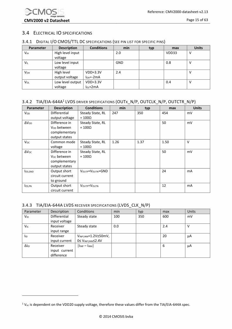
3.4 ELECTRICAL IO SPECIFICATIONS
3.4.1 DIGITAL I/O CMOS/TTL DC SPECIFICATIONS (SEE PIN LIST FOR SPECIFIC PINS)
Parameter Description Conditions min typ max Units
VIH High level input voltage
2.0 VDD33 V
VIL Low level input voltage
GND 0.8 V
VOH High level output voltage
VDD=3.3V IOH=-2mA
2.4 V
VOL Low level output voltage
VDD=3.3V IOL=2mA
0.4 V
3.4.2 TIA/EIA-644A1 LVDS DRIVER SPECIFICATIONS (OUTX_N/P, OUTCLK_N/P, OUTCTR_N/P)
Parameter Description Conditions min typ max Units
VOD Differential output voltage
Steady State, RL = 100Ω
247 350 454 mV
∆VOD Difference in VOD between complementary output states
Steady State, RL = 100Ω
50 mV
VOC Common mode voltage
Steady State, RL = 100Ω
1.26 1.37 1.50 V
∆VOC Difference in VOC between complementary output states
Steady State, RL = 100Ω
50 mV
IOS,GND Output short circuit current to ground
VOUTP=VOUTN=GND 24 mA
IOS,PN Output short circuit current
VOUTP=VOUTN 12 mA
3.4.3 TIA/EIA-644A LVDS RECEIVER SPECIFICATIONS (LVDS_CLK_N/P)
Parameter Description Conditions min typ max Units
VID Differential input voltage
Steady state 100 350 600 mV
VIC Receiver input range
Steady state 0.0 2.4 V
IID Receiver input current
VINP|INN=1.2V±50mV, 0≤ VINP|INN≤2.4V
20 µA
∆IID Receiver input current difference
|IINP – IINN| 6 µA
1 Voc is dependent on the VDD20 supply voltage, therefore these values differ from the TIA/EIA-644A spec.

Reference: CMV2000-datasheet-v2.13
CMV2000 v2 Datasheet Page 16 of 63
© 2014 CMOSIS bvba
3.5 INPUT CLOCK
The high speed LVDS input clock (LVDS_CLK_N/P) defines the output data rate of the CMV2000. The master clock
(CLK_IN) must be 10 or 12 times slower depending on the programmed bit mode setting. The maximum data rate of the
output is 480Mbps which results in a LVDS_CLK_N/P of 480MHz and a CLK_IN of 48MHz in 10-bit mode and 40MHz in
12-bit mode. The minimum frequencies are 5MHz for CLK_IN and 50MHz for LVDS_CLK_N/P. Any frequency between
the minimum and maximum can be applied by the user and will result in a corresponding output data rate.
CLK_IN LVDS_CLK 10bit LVDS_CLK 12bit
5 MHz 50 MHz 60 MHz
40 MHz 400 MHz 480 MHz
48 MHz 480 MHz n/a
The rising edge LVDS input clock can have a limited delay with respect to the rising edge of the master input clock,
depending on clock speed. In Figure 5 below, the skew limits are shown for different clock speeds and for an LVDS clock
that rises before and after the master input clock. To assure proper working of the sensor, the skew of the LVDS clock
should always fall within these limits, shown as the green area.
1400
780
1680
660
CLK_IN
LVDS_CLK 400MHz
LVDS_CLK 350MHz
LVDS_CLK 300MHz
640
LVDS_CLK 250MHz
680
LVDS_CLK 200MHz
1145
600
1240
580
LVDS_CLK 480MHz
LVDS_CLK 450MHz
FIGURE 5: LVDS CLOCK DELAY VERSUS MASTER CLOCK

Reference: CMV2000-datasheet-v2.13
CMV2000 v2 Datasheet Page 17 of 63
© 2014 CMOSIS bvba
3.6 FRAME RATE CALCULATION
The frame rate is defined by 2 main factors.
1. Exposure time
2. Read-out time
To simplify the calculation we will assume that the exposure time is shorter than the read-out time and that the sensor
is operating at default settings, taking a full resolution 10-bit image at 48MHz through 16 outputs. This means that the
frame rate will be defined only by the read-out time because the exposure time happens in parallel with the read-out.
The read-out time is defined by:
1. Output clock speed: max 240MHz
2. ADC mode: 10 or 12 bit
3. Number of lines read-out
4. Number of LVDS outputs used: max 16 outputs
If any of these parameters is changed, it will have an impact on the frame rate. In default operation this will result in
340FPS. The total read-out time is composed of two parts: FOT (frame overhead time) and image read-out time.
The FOT is defined as:
𝐹𝑂𝑇 = (𝑓𝑜𝑡_𝑙𝑒𝑛𝑔𝑡ℎ + (2 ∗16
#𝑜𝑢𝑡𝑝𝑢𝑡𝑠 𝑢𝑠𝑒𝑑)) ∗ 129 ∗ 𝑚𝑎𝑠𝑡𝑒𝑟 𝑐𝑙𝑜𝑐𝑘 𝑝𝑒𝑟𝑖𝑜𝑑
With fot_length (register 73) at its default value of 10, this results in 32.25µs frame overhead time.
The image read-out time is defined as:
𝐼𝑚𝑎𝑔𝑒 𝑟𝑒𝑎𝑑-𝑜𝑢𝑡 𝑡𝑖𝑚𝑒 = (129 ∗ 𝑚𝑎𝑠𝑡𝑒𝑟 𝑐𝑙𝑜𝑐𝑘 𝑝𝑒𝑟𝑖𝑜𝑑 ∗16
#𝑜𝑢𝑡𝑝𝑢𝑡𝑠 𝑢𝑠𝑒𝑑) ∗ 𝑛𝑟_𝑙𝑖𝑛𝑒𝑠
Reading out a full resolution image, this results in 2.924ms image read-out time.
The total read-out time is now the sum of the FOT and the image read-out time, which results in 32.25µs + 2.924ms or
2.9525ms to read out a single full resolution image. The frame rate is thus 338FPS.
The table below gives some examples of how the frame rate increases when reading out a smaller frame in 10 bit
mode.
Number of columns Number of lines Frame rate [FPS]
2048 1088 338
2048 512 710
2048 70 4537
FRAME_REQ
Frame1_cycle FOT Read-out time
Exposure timeFrame2_cycle FOT Read-out time
Exposure time
Frame period
FIGURE 6: FRAME PERIOD
When the exposure time is greater than the read-out time, the frame rate is mostly defined by the exposure time itself (as the exposure time will be much longer than the FOT).

Reference: CMV2000-datasheet-v2.13
CMV2000 v2 Datasheet Page 18 of 63
© 2014 CMOSIS bvba
3.7 START-UP SEQUENCE
The sequence as described in Figure 6 should be followed when the sensor is started up in default output mode
(480Mbps, 10bit resolution). There is no specific startup sequence for the power supplies needed.
1μs
1μs
Stable time
Supply
CLK_IN
SYS_RES_N
FRAME_REQ
FIGURE 7: START-UP SEQUENCE FOR 480MBPS @ 10-BIT
The CLK_IN master clock (48MHz for 480Mbps in 10-bit mode) should only start after the rise time of the supplies. The
external reset pin should be released at least 1μs after the supplies have become stable. The first frame can be
requested 1μs after the reset pin has been released.
If the register settings need to be changed (e.g. when using 12-bit mode), this can be done through an SPI upload 1µs
after the rising edge on the SYS_RES_N pin, as described in Figure 9. In this case, the FRAME_REQ pulse must not be
sent until after the SPI upload is completed, plus a settling time. This settling time is to ensure that the changes
programmed in the SPI upload have taken effect before an image is captured. The main factor that determines this
settling time is the change in ADC gain, because the voltage over the ramp capacitor has to settle. For typical
applications, where the ADC gain is changed from the default value of 32 to a value that saturates the ADC output (40
to 45 at 48MHz), the settling time is 5ms. In extreme cases, when the gain is changed from default to the maximum
value, the settling time will increase to 20ms.
1μsStable time
Supply
CLK_IN
SYS_RES_N
FRAME_REQ
SPI uploadSPI upload
1μs
Settling time
FIGURE 8: START-UP SEQUENCE FOR 12-BIT MODE
Reference: CMV2000-datasheet-v2.13
CMV2000 v2 Datasheet Page 19 of 63
© 2014 CMOSIS bvba
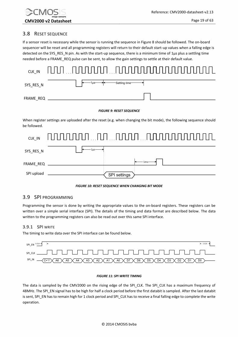
3.8 RESET SEQUENCE
If a sensor reset is necessary while the sensor is running the sequence in Figure 8 should be followed. The on-board
sequencer will be reset and all programming registers will return to their default start-up values when a falling edge is
detected on the SYS_RES_N pin. As with the start-up sequence, there is a minimum time of 1µs plus a settling time
needed before a FRAME_REQ pulse can be sent, to allow the gain settings to settle at their default value.
CLK_IN
SYS_RES_N
FRAME_REQ
1µs Settling time
FIGURE 9: RESET SEQUENCE
When register settings are uploaded after the reset (e.g. when changing the bit mode), the following sequence should
be followed.
1μs
CLK_IN
SYS_RES_N
FRAME_REQ
SPI settingsSPI upload
1ms
FIGURE 10: RESET SEQUENCE WHEN CHANGING BIT MODE
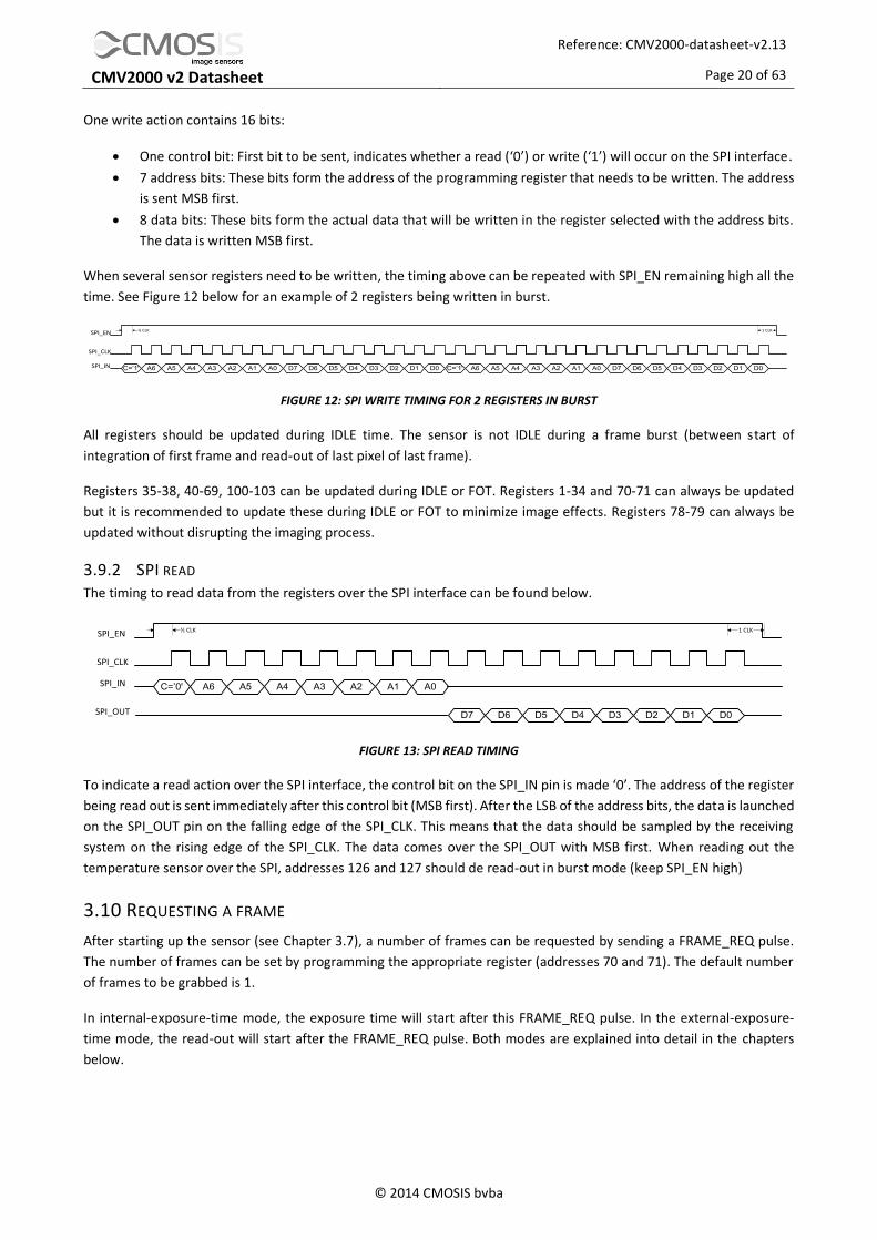
3.9 SPI PROGRAMMING
Programming the sensor is done by writing the appropriate values to the on-board registers. These registers can be
written over a simple serial interface (SPI). The details of the timing and data format are described below. The data
written to the programming registers can also be read out over this same SPI interface.
3.9.1 SPI WRITE
The timing to write data over the SPI interface can be found below.
SPI_EN
SPI_IN
SPI_CLK
C=’1' A6 A5 A4 A3 A2 A1 A0 D7 D6 D5 D4 D3 D2 D1 D0
½ CLK 1 CLK
FIGURE 11: SPI WRITE TIMING
The data is sampled by the CMV2000 on the rising edge of the SPI_CLK. The SPI_CLK has a maximum frequency of
48MHz. The SPI_EN signal has to be high for half a clock period before the first databit is sampled. After the last databit
is sent, SPI_EN has to remain high for 1 clock period and SPI_CLK has to receive a final falling edge to complete the write
operation.
Reference: CMV2000-datasheet-v2.13
CMV2000 v2 Datasheet Page 20 of 63
© 2014 CMOSIS bvba
One write action contains 16 bits:
One control bit: First bit to be sent, indicates whether a read (‘0’) or write (‘1’) will occur on the SPI interface.
7 address bits: These bits form the address of the programming register that needs to be written. The address
is sent MSB first.
8 data bits: These bits form the actual data that will be written in the register selected with the address bits.
The data is written MSB first.
When several sensor registers need to be written, the timing above can be repeated with SPI_EN remaining high all the
time. See Figure 12 below for an example of 2 registers being written in burst.
SPI_EN
SPI_IN
SPI_CLK
C=’1' A6 A5 A4 A3 A2 A1 A0 D7 D6 D5 D4 D3 D2 D1 D0 C=’1' A6 A5 A4 A3 A2 A1 A0 D7 D6 D5 D4 D3 D2 D1 D0
½ CLK 1 CLK
FIGURE 12: SPI WRITE TIMING FOR 2 REGISTERS IN BURST
All registers should be updated during IDLE time. The sensor is not IDLE during a frame burst (between start of
integration of first frame and read-out of last pixel of last frame).
Registers 35-38, 40-69, 100-103 can be updated during IDLE or FOT. Registers 1-34 and 70-71 can always be updated
but it is recommended to update these during IDLE or FOT to minimize image effects. Registers 78-79 can always be
updated without disrupting the imaging process.
3.9.2 SPI READ The timing to read data from the registers over the SPI interface can be found below.
SPI_EN
SPI_IN
SPI_CLK
C=’0' A6 A5 A4 A3 A2 A1 A0
D7 D6 D5 D4 D3 D2 D1 D0SPI_OUT
½ CLK 1 CLK
FIGURE 13: SPI READ TIMING
To indicate a read action over the SPI interface, the control bit on the SPI_IN pin is made ‘0’. The address of the register
being read out is sent immediately after this control bit (MSB first). After the LSB of the address bits, the data is launched
on the SPI_OUT pin on the falling edge of the SPI_CLK. This means that the data should be sampled by the receiving
system on the rising edge of the SPI_CLK. The data comes over the SPI_OUT with MSB first. When reading out the
temperature sensor over the SPI, addresses 126 and 127 should de read-out in burst mode (keep SPI_EN high)
3.10 REQUESTING A FRAME
After starting up the sensor (see Chapter 3.7), a number of frames can be requested by sending a FRAME_REQ pulse.
The number of frames can be set by programming the appropriate register (addresses 70 and 71). The default number
of frames to be grabbed is 1.
In internal-exposure-time mode, the exposure time will start after this FRAME_REQ pulse. In the external-exposure-
time mode, the read-out will start after the FRAME_REQ pulse. Both modes are explained into detail in the chapters
below.

Reference: CMV2000-datasheet-v2.13
CMV2000 v2 Datasheet Page 21 of 63
© 2014 CMOSIS bvba
3.10.1 INTERNAL EXPOSURE CONTROL In this mode, the exposure time is set by programming the appropriate registers (address 42-44) of the CMV2000. After
the high state of the FRAME_REQ pulse is detected, the exposure time will start after a delay of 133 clock cycles, see
AN16 – Exposure Timings for all the timing details. When the exposure time ends, the pixels are sampled and prepared
for read-out. This sequence is called the frame overhead time (FOT). Immediately after the FOT, the frame is read-out
automatically. If more than one frame is requested, the exposure of the next frame starts already during the read-out
of the previous one. See the diagram below for more details.
FRAME_REQ
Exposure timeFrame1_cycle FOT Read-out time
Exposure timeFrame2_cycle FOT Read-out time
FIGURE 14: REQUEST FOR 2 FRAMES IN INTERNAL- EXPOSURE-TIME MODE
When the exposure time is shorter than the read-out time, the FOT and read-out of the next frame will start immediately
after the read-out of the previous frame. Keep in mind that the next FRAME_REQ pulse has to occur after the FOT of
the current frame. For an exact calculation of the exposure time see Chapter 5.1.
FRAME_REQ
Frame1_cycle FOT Read-out time
Exposure timeFrame2_cycle FOT Read-out time
Exposure time
FIGURE 15: REQUEST FOR 2 FRAMES IN INTERNAL EXPOSURE MODE WITH EXPOSURE TIME < READ-OUT TIME
If a next FRAME_REQ pulse is applied during exposure time or FOT of the current frame, it will be ignored and no new
frame is requested. FRAME_REQ should occur during or after the read-out time of the current frame.
If the exposure time is shorter than the read-out time, keep in mind that when you apply a next FRAME_REQ pulse
during the read-out of the current frame, the exposure of that new frame will start immediately. So you have to keep
enough time between the two FRAME_REQ pulses so the read-out times don’t overlap. If the FOT of the next frame
starts during the read-out of the current frame, that read-out will be aborted immediately as shown in Figure 16. If the
exposure time is longer than the read-out time, the read-out times of two consecutive frames can’t overlap and won’t
cause a problem. The minimum time between two FRAME_REQ pulses should be:
𝑒𝑥𝑝𝑜𝑠𝑢𝑟𝑒 𝑡𝑖𝑚𝑒 + 𝐹𝑂𝑇 + (𝑅𝑒𝑎𝑑𝑜𝑢𝑡 𝑡𝑖𝑚𝑒 − 𝐸𝑥𝑝𝑜𝑠𝑢𝑟𝑒 𝑡𝑖𝑚𝑒) = 𝐹𝑂𝑇 + 𝑅𝑒𝑎𝑑𝑜𝑢𝑡 𝑡𝑖𝑚𝑒

Reference: CMV2000-datasheet-v2.13
CMV2000 v2 Datasheet Page 22 of 63
© 2014 CMOSIS bvba
FRAME_REQ
Frame1_cycle FOT Read-out time
Exposure timeFrame2_cycle FOT
Exposure time
Read-out time
FRAME_REQ
Frame1_cycle FOT Read-out time
Exposure timeFrame2_cycle FOT
Exposure time
Read-out time
FRAME_REQ
Frame1_cycle FOT Lost ROTRead-out time
Exposure timeFrame2_cycle FOT
Exposure time
Read-out time
FIGURE 16: THE TIMING EFFECT OF TWO REQUESTS FOR 1 FRAME IN INTERNAL EXPOSURE MODE
3.10.2 EXTERNAL EXPOSURE TIME The exposure time can also be programmed externally by using the T_EXP1 input pin. This mode needs to be enabled
by setting the appropriate register (address 41). In this case, the exposure starts when a high state is detected on the
T_EXP1 pin. When a high state is detected on the FRAME_REQ input, the exposure time stops and the read-out will start
automatically. A new exposure can start by sending a pulse to the T_EXP1 pin during or after the read-out of the previous
frame. The minimum time between T_EXP1 and FRAME_REQ is 1 master clock cycle and between FRAME_REQ and
T_EXP1 is FOT. For an exact calculation of the exposure time see Chapter 5.1.
FRAME_REQ
Exposure timeFrame1_cycle FOT Read-out time
Exposure timeFrame2_cycle FOT Read-out time
T_EXP1
FIGURE 17: REQUEST FOR 2 FRAMES USING EXTERNAL-EXPOSURE-TIME MODE

Reference: CMV2000-datasheet-v2.13
CMV2000 v2 Datasheet Page 23 of 63
© 2014 CMOSIS bvba
4 READING OUT THE SENSOR
4.1 LVDS DATA OUTPUTS
The CMV2000 has LVDS (low voltage differential signaling) outputs to transport the image data to the surrounding
system. Next to 16 data channels, the sensor also has two other LVDS channels for control and synchronization of the
image data. In total, the sensor has 18 LVDS output pairs (2 pins for each LVDS channel):
16 Data channels
1 Control channel
1 Clock channel
This means that a total of 36 pins of the CMV2000 are used for the LVDS outputs (32 for data + 2 for LVDS clock + 2 for
control channel). See the pin list for the exact pin numbers of the LVDS outputs.
The 16 data channels are used to transfer the 10-bit or 12-bit pixel data from the sensor to the receiver in the
surrounding system.
The output clock channel transports a clock, synchronous to the data on the other LVDS channels. This clock can be
used at the receiving end to sample the data. This clock is a DDR clock which means that the frequency will be half of
the output data rate. When 480Mbps output data rate is used, the LVDS output clock will be 240MHz.
The data on the control channel contains status information on the validity of the data on the data channels. Information
on the control channel is grouped in 10-bit or 12-bit words that are transferred synchronous to the 16 data channels.
4.2 LOW-LEVEL PIXEL TIMING Figure 18 and Figure 19 show the timing for transfer of 10-bit and 12-bit pixel data over one LVDS output. To make the
timing more clear, the figures show only the p-channel of each LVDS pair. The data is transferred LSB first, with the
transfer of bit D0 during the high phase of the DDR output clock OUTCLK.
D8 D9 D0 D1 D2 D3 D4 D5 D6 D7 D8 D9 D0 D1 D2 D3
T1
OUTCLK_P
OUTX_P
FIGURE 18: 10-BIT PIXEL DATA ON AN LVDS CHANNEL
The time ‘T1’ in Figure 18 is 1/10th of the period of the CLK_IN input clock. If a frequency of 48MHz is used for CLK_IN
(max in 10-bit mode) and 480MHz for LVDS_CLK_N/P this results in a 240MHz OUTCLK frequency.
D10 D11 D0 D1 D2 D3 D4 D5 D6 D7 D8 D9 D10 D11 D0 D1
T2
OUTCLK_P
OUTX_P
FIGURE 19: 12-BIT PIXEL DATA ON AN LVDS CHANNEL
The time ‘T2’ in Figure 19 is 1/12th of the period of the CLK_IN input clock. When a frequency of 40MHz is used for
CLK_IN (max in 12-bit mode) and 480MHz for LVDS_CLK_N/P this results in a 240MHz OUTCLK frequency.

Reference: CMV2000-datasheet-v2.13
CMV2000 v2 Datasheet Page 24 of 63
© 2014 CMOSIS bvba
4.3 READ-OUT TIMING The read-out of image data is grouped in bursts of 128 pixels per channel. Each pixel is either 10 or 12 bits of data (see
Chapter 4.2). One complete pixel period equals one period of the input clock CLK_IN. For details on pixel remapping
and pixel vs. channel location please see Chapter 4.4 of this document. An overhead time exists between two bursts of
128 pixels. This overhead time has the same length of one pixel read-out (i.e. the length of 10 or 12 bits at the selected
data rate or one CLK_IN period). For details on how to program the sequencer for different output modes, see Chapter
5.7.
4.3.1 10 BIT MODE In this chapter, the read-out timing for the default 10 bit mode is explained. In this mode the maximum frame rate of
340FPS can be reached. To simplify the figures below, the timing for only one LVDS channel is shown in every case.
4.3.1.1 16 OUTPUT CHANNELS
By default, all 16 data output channels are used to transmit the image data. This means that an entire row of image data
is transferred in one slot of 128 pixel periods (16 x 128 = 2048). This results in a maximum frame rate of 340FPS.
IDLE OH 128 OHDATA_OUT 128 OH 128 OH 128
Row 1 Row 2 Row 3 Row 4
FIGURE 20: OUTPUT TIMING IN DEFAULT 16 CHANNEL MODE
4.3.1.2 8 OUTPUT CHANNELS
When only 8 LVDS output channels are used, the read-out of one row takes (2*128) + (2*1) CLK_IN periods. The
maximum frame rate is reduced with a factor of 2 compared to 16 channel mode.
IDLE OH 128 OHDATA_OUT 128 OH 128 OH 128
Row 1 Row 2
FIGURE 21: OUTPUT TIMING IN 8 CHANNEL MODE
4.3.1.3 4 OUTPUT CHANNELS
When only 4 LVDS output channels are used, the read-out of one row takes (4*128) + (4*1) CLK_IN periods. The
maximum frame rate is reduce with a factor of 4 compared to 16 channel mode.
IDLE OH 128 OHDATA_OUT 128 OH 128 OH 128
Row 1 Row 2
OH 128 OH 128 OH 128 OH 128
FIGURE 22: OUTPUT TIMING IN OF 4 CHANNEL MODE
4.3.1.4 2 OUTPUT CHANNELS
When only 2 LVDS output channels are used, the read-out of one row takes (8*128) + (8*1) CLK_IN periods. The
maximum frame rate is reduced with a factor of 8 compared to 16 channel mode.
IDLE OH 128 128 128 128 128
Row 1
128 128 128 128 128 128 128 128
Row 2
128 128 128OH OH OH OH OH OH OH OH OH OH OH OH OH OH OH
FIGURE 23: OUTPUT TIMING IN 2 CHANNEL MODE

Reference: CMV2000-datasheet-v2.13
CMV2000 v2 Datasheet Page 25 of 63
© 2014 CMOSIS bvba
4.3.2 12 BIT MODE In 12 bit mode, the analog-to-digital conversion takes 4x longer to complete. This causes the frame rate to drop to 70FPS
when 480MHz is used for LVDS_CLK_N/P. Due to this extra conversion time, the sensor automatically multiplexes to 4
outputs when 12 bit is used. To simplify the figures below, the timing for only one LVDS channel is shown in every case.
4.3.2.1 4 OUTPUT CHANNELS
By default, the CMV2000 uses only 4 LVDS output channels in 12 bit mode. This means that the read-out of one row
takes (4*128) + (4*1) CLK_IN periods.
IDLE OH 128 OHDATA_OUT 128 OH 128 OH 128
Row 1 Row 2
OH 128 OH 128 OH 128 OH 128
FIGURE 24: OUTPUT TIMING IN OF 4 CHANNEL MODE
4.3.2.2 2 OUTPUT CHANNELS
When only 2 LVDS output channels are used, the read-out of one row takes (8*128) + (8*1) CLK_IN periods. The
maximum frame rate is reduced with a factor of 2 compared to 4-channel mode.
IDLE OH 128 128 128 128 128
Row 1
128 128 128 128 128 128 128 128
Row 2
128 128 128OH OH OH OH OH OH OH OH OH OH OH OH OH OH OH
FIGURE 25: OUTPUT TIMING IN 2 CHANNEL MODE
4.4 PIXEL REMAPPING
Depending on the number of output channels, the pixels are read out by different channels and come out at a different
moment in time. With the details from the next chapters, the end user is able to remap the pixel values at the output
to their correct image array location.
4.4.1 16 OUTPUTS Figure 26 below shows the location of the image pixels versus the output channel of the image sensor.
16 bursts of 128 pixels happen in parallel on the data outputs. This means that one complete row is read out in one
burst. The amount of rows that will be read out depends on the value in the corresponding register. By default there
are 1088 rows being read out.
IDLE Pixel 0 to 127Channel 1
IDLE Pixel 128 to 255Channel 2
IDLE Pixel 256 to 383Channel 3
IDLE Pixel 1792 to 1919Channel 15
IDLE Pixel 1920 to 2047Channel 16
Row 1
Pixel 0 to 127
Row 2
Pixel 128 to 255
Pixel 256 to 383
Pixel 1792 to 1919
Pixel 1920 to 2047
FIGURE 26: PIXEL REMAPPING FOR 16 OUTPUT CHANNELS

Reference: CMV2000-datasheet-v2.13
CMV2000 v2 Datasheet Page 26 of 63
© 2014 CMOSIS bvba
4.4.2 8 OUTPUTS When only 8 outputs are used, the pixel data is placed on the outputs as detailed in Figure 27. 8 bursts of 128 pixels
happen in parallel on the data outputs. This means that one complete row is read out in two bursts. The time needed
to read out one row is doubled compared to when 16 outputs are used. Channel 2, 4, 6…16 are not being used in this
mode, so they can be turned off by setting the correct bits in the register with addresses 80-82. Turning off these
channels will reduce the power consumption of the chip.
The amount of rows that will be read out can be set in the register. By default there are 1088 rows being read out.
IDLE Pixel 0 to 127Channel 1
IDLE
Pixel 128 to 255
Channel 3
IDLE
Pixel 256 to 383
Channel 5
IDLE
Pixel 1792 to 1919
Channel 13
IDLE
Pixel 1536 to 1663
Channel 15
Row 1
Pixel 384 to 511
Pixel 512 to 639
Pixel 1664 to 1791
Pixel 1920 to 2047
Pixel 640 to 767
FIGURE 27: PIXEL REMAPPING FOR 8 OUTPUT CHANNELS
4.4.3 4 OUTPUTS When only 4 outputs are used, the pixel data is placed on the outputs as detailed in Figure 28. 4 bursts of 128 pixels
happen in parallel on the data outputs. This means that one complete row is read out in four bursts. The time needed
to read out one row is 4x longer compared to when 16 outputs are used. Only channel 1, 5, 9 and 13 are being used in
this mode, so the remaining channels can be turned off by setting the correct bits in the register with addresses 80-82.
Turning off these channels will reduce the power consumption of the chip.
The amount of rows that will be read out can be set in the register. By default there are 1088 rows being read out.
IDLE Pixel 0 to 127Channel 1
IDLE
Pixel 128 to 255
Channel 5
IDLE
Pixel 256 to 383
Channel 9
IDLEChannel 13 Pixel 1536 to 1663
Row 1
Pixel 384 to 511
Pixel 512 to 639
Pixel 1664 to 1791
Pixel 640 to 767 Pixel 768 to 895 Pixel 896 to 1023
Pixel 1024 to 1151 Pixel 1152 to 1279 Pixel 1280 to 1407 Pixel 1408 to 1535
Pixel 1792 to 1919 Pixel 1920 to 2047
FIGURE 28: PIXEL REMAPPING FOR 4 OUTPUT CHANNELS
4.4.4 2 OUTPUTS When only 2 outputs are used, the pixel data is placed on the outputs as detailed in Figure 29. 2 bursts of 128 pixels
happen in parallel on the data outputs. This means that one complete row is read out in 8 bursts. The time needed to
read out one row is 8x longer compared to when 16 outputs are used. Only channel 1 and 9 are being used in this mode,
so the remaining channels can be turned off by setting the correct bits in the register with addresses 80-82. Turning off
these channels will reduce the power consumption of the chip.
The amount of rows that will be read out can be set in the register. By default there are 1088 rows being read out.
IDLE Pixel 0 to 127Channel 1
IDLE
Pixel 128 to 255
Channel 9
Pixel 256 to 383
Pixel 1536 to 1663
Row 1
Pixel 384 to 511 Pixel 512 to 639
Pixel 1664 to 1791
Pixel 640 to 767 Pixel 768 to 895 Pixel 896 to 1023
Pixel 1024 to 1151 Pixel 1152 to 1279 Pixel 1280 to 1407 Pixel 1408 to 1535 Pixel 1792 to 1919 Pixel 1920 to 2047
FIGURE 29: PIXEL REMAPPING FOR 2 OUTPUT CHANNELS
Reference: CMV2000-datasheet-v2.13
CMV2000 v2 Datasheet Page 27 of 63
© 2014 CMOSIS bvba
4.4.5 OVERVIEW All outputs are always used to send data, but if you use less than 16 channels, some channels will have duplicate data.
For example if you multiplex to 4 channels, outputs 6, 7 and 8 will have identical data as output 5. Below you see an
overview of which channel data is on which output at a certain output mode.
MUX to
OUT 1
OUT 2
OUT 3
OUT 4
OUT 5
OUT 6
OUT 7
OUT 8
OUT 9
OUT 10
OUT 11
OUT 12
OUT 13
OUT 14
OUT 15
OUT 16
16 CH1 CH2 CH3 CH4 CH5 CH6 CH7 CH8 CH9 CH10 CH11 CH12 CH13 CH14 CH15 CH16
8 CH1 CH1 CH3 CH3 CH5 CH5 CH7 CH7 CH9 CH9 CH11 CH11 CH13 CH13 CH15 CH15
4 CH1 CH1 CH1 CH1 CH5 CH5 CH5 CH5 CH9 CH9 CH9 CH9 CH13 CH13 CH13 CH13
2 CH1 CH1 CH1 CH1 CH1 CH1 CH1 CH1 CH9 CH9 CH9 CH9 CH9 CH9 CH9 CH9
4.5 CONTROL CHANNEL The CMV2000 has one LVDS output channel dedicated for the valid data synchronization and timing of the output
channels. The end user must use this channel to know when valid image data or training data is available on the data
output channels. Data is transferred in 10-bit or 12-bit word format. Every bit has a specific function, which is described
in the following table, but only the DVAL, LVAL and FVAL signal are necessary to know when to sample the image data.
Bit Function Description
[0] DVAL Indicates valid pixel data on the outputs
[1] LVAL Indicates validity of the read-out of a row
[2] FVAL Indicates the validity of the read-out of a frame
[3] SLOT Indicates the overhead period before 128-pixel bursts (*)
[4] ROW Indicates the overhead period before the read-out of a row (*)
[5] FOT Indicates when the sensor is in FOT (sampling of image data in pixels) (*)
[6] INTE1 Indicates when pixels of integration block 1 are integrating (*)
[7] INTE2 Indicates when pixels of integration block 2 are integrating (*)
[8] ‘0’ Constant zero
[9] ‘1’ Constant one
[10] ‘0’ Constant zero
[11] ‘0’ Constant zero
(*)Note: These bits are purely informational and are not required to know when the data is valid.
INTE1 and INTE2 will be low when FOT is high, so the exposure during the 0.43*fot_length overlap (see Chapter 5.1),
will not be visible in the INTE1 and INTE2 bits.
Pins H2 (TDIG1) and G2 (TDIG2) can be programmed to map the state of control channel bits [0] (DVAL), [1] (LVAL), [2]
(FVAL), [6] (INTE1) or [7] (INTE2) with registers 108 (T_dig1) and 109 (T_dig2).
Register 108/109 Value TDIG1 TDIG2
0 INTE1 INTE1
1 INTE2 INTE2
2 DVAL DVAL
3 LVAL LVAL
4 FVAL FVAL

Reference: CMV2000-datasheet-v2.13
CMV2000 v2 Datasheet Page 28 of 63
© 2014 CMOSIS bvba
4.5.1 DVAL, LVAL, FVAL
The first three bits of the control word must be used to identify valid data and the read-out status.
Next figure shows the timing of the DVAL, LVAL and FVAL bits of the control channel with an example of the read-out of
a frame of 3 rows (default is 1088 rows). This example uses the default mode of 16 outputs in 10 bit mode.
IDLE OH 128 OH 128 OH 128DATA_OUT
DVAL
LVAL
FVAL
FIGURE 30: DVAL, LVAL AND FVAL TIMING IN 16 OUTPUT MODE
When only 8 outputs are used, the line read-out time is 2x longer. The control channel takes this into account and the
timing in this mode is shown in Figure 31 and Figure 32. The timing extrapolates identically for 4 and 2 outputs.
IDLE OH 128 OH 128 OH 128DATA_OUT
DVAL
LVAL
FVAL
OH 128 OH 128 OH 128
FIGURE 31: DVAL, LVAL AND FVAL TIMING IN 8 OUTPUT MODE
OH 128 OH 128 OH 128DATA_OUT
DVAL
LVAL
FVAL
OH 128 OH 128 OH 128
Exposure 1 Read-out 1FOTFrames
cycleExposure 2 Read-out 2FOT
DVAL [0]
LVAL [1]
FVAL [2]
SLOT [3]
ROW [4]
FOT [5]
INTE1 [6]
INTE2 [7]
10 0000 0000
Data
CTRL_OUT
Data
Data
Data
Data
Data
Data
Data
Data
Data
10 000x xxxx 10 1100 0000 10 0010 0000 10 000x xxxx
Training PatternDATA_OUT Data Training Data Training Pattern
10 1100 0000 10 0010 0000 10 0000 000010 110x xxxx
Read-out 1
Exposure 2
Frames
cycle
SLOT
ROW
FOT
INTE1
INTE2
10 0001
1000CTRL_OUT 10 0000 0111 10 0000
1110 10 0000 0111 10 0001
1100 10 0000 0111 10 0000
1110 10 0000 0111 10 0001 0011 10 0000 0111
10 1100 1110 10 1100 011110 1100 0111
10 bit, 8 outputs, single window of 3 lines
FIGURE 32: DETAILED TIMINGS OF THE CONTROL CHANNEL (8 OUTPUTS, 3 LINES WINDOW)

Reference: CMV2000-datasheet-v2.13
CMV2000 v2 Datasheet Page 29 of 63
© 2014 CMOSIS bvba
4.6 TRAINING DATA To synchronize the receiving side with the LVDS outputs of the CMV2000, a known data pattern can be put on the output
channels. This pattern can be used to “train” the LVDS receiver of the surrounding system to achieve correct word
alignment of the image data. Such a training pattern is put on all 16 data channel outputs when there is no valid image
data to be sent (so, also in between bursts of 128 pixels). The training pattern is a 10-bit or 12-bit data word that
replaces the pixel data. The sensor has a 12-bit sequencer register (address 78-79) that can be loaded through the SPI
to change the contents of the 12-bit training pattern.
The control channel does not send a training pattern, because it is used to send control information at all time. Word
alignment can be done on this channel when the sensor is idle (not exposing or sending image data). In this case all bits
of the control word are zero, except for bit [9] (= 0010 0000 0000 or 512 decimal).
Figure 33 shows the location of the training pattern (TP) on the data channels and control channels when the sensor is
in idle mode and when a frame of 3 rows is read-out. The default mode of 16 outputs is selected.
Training pattern TP 128 TP 128 TP 128Data
channels
DVAL
LVAL
FVAL
Control
channel0010 0000 0000 Control information
Sensor in idle mode
FIGURE 33: TRAINING PATTERN LOCATION IN THE DATA AND CONTROL CHANNELS

Reference: CMV2000-datasheet-v2.13
CMV2000 v2 Datasheet Page 30 of 63
© 2014 CMOSIS bvba
5 IMAGE SENSOR PROGRAMMING This section explains how the CMV2000 can be programmed using the on-board sequencer registers.
5.1 EXPOSURE MODES
The exposure time can be programmed in two ways, externally or internally. Externally, the exposure time is defined as
the time between the rising edge of T_EXP1 and the rising edge of FRAME_REQ (see Chapter 3.10.2 for more details).
Internally, the exposure time is set by uploading the desired value to the corresponding sequencer register.
The table below gives an overview of the registers involved in the exposure mode.
Exposure time settings
Register name Register address Default value Description of the value
Exp_ext 41[0] 0 0: Use registers for defining integration time 1: Use external signals T_EXP1 and FRAME_REQ for integration control
Exp_time 42[7:0] 43[7:0] 44[7:0]
1088 If Exp_ext = ‘0’: Defines the exposure time according to the following formula:
129 ∗ 𝑐𝑙𝑘_𝑝𝑒𝑟(0.43 ∗ 𝑓𝑜𝑡_𝑙𝑒𝑛𝑔𝑡ℎ + 𝐸𝑥𝑝_𝑡𝑖𝑚𝑒)
Where clk_per is the period of the CLK_IN input clock and fot_length is the value in register 73. If Exp_ext = ‘1’: The exposure time is:
129 ∗ 𝑐𝑙𝑘_𝑝𝑒𝑟(0.43 ∗ 𝑓𝑜𝑡_𝑙𝑒𝑛𝑔𝑡ℎ) + 𝑒𝑥𝑡𝑒𝑟𝑛𝑎𝑙 𝑒𝑥𝑝𝑜𝑠𝑢𝑟𝑒 𝑡𝑖𝑚𝑒
Where external exposure time is the time between the T_EXP1 and FRAME_REQ pulses.
To calculate back from actual exposure time to the register value for internal exposure you can use the following formula
(exposure time and clk_per should have the same time unit):
𝐸𝑥𝑝_𝑡𝑖𝑚𝑒 =𝑒𝑥𝑝𝑜𝑠𝑢𝑟𝑒 𝑡𝑖𝑚𝑒
129 ∗ 𝑐𝑙𝑘𝑝𝑒𝑟
− 0.43 ∗ 𝑓𝑜𝑡_𝑙𝑒𝑛𝑔𝑡ℎ
For very short integration times, the fot_length should be lowered to 5 and the maximum clock speed should be used.
In internal exposure mode, the shortest exposure time is limited by the exp_time register, when this is set to 1, the
shortest exposure time is 14.24µs, or 8.47µs for fot_length = 5.
In external exposure mode, the time between T_EXP1 and FRAME_REQ can be as short as one clock cycle, reducing the
shortest exposure time even more to 11.58µs, or 5.80µs for fot_length = 5.
5.2 HIGH DYNAMIC RANGE MODES
The sensor has different ways to achieve high optical dynamic range in the grabbed image.
Interleaved read-out: the odd and even rows have a different exposure time
Piecewise linear response: pixels respond to light with a piecewise linear response curve.
Multi-frame read-out: Different frames are read-out with increasing exposure time

Reference: CMV2000-datasheet-v2.13
CMV2000 v2 Datasheet Page 31 of 63
© 2014 CMOSIS bvba
All the HDR modes mentioned above can be used in both the internal and external exposure time mode.
5.2.1 INTERLEAVED READ-OUT In this HDR mode, the odd and even rows of the image sensors will have a different exposure time. This mode can be
enabled by setting the register in the table below.
HDR settings – interleaved read-out
Register name Register address Default value Description of the value
Exp_dual 41[1] 0 0: interleaved exposure mode disabled 1: interleaved exposure mode enabled
The surrounding system can combine the image of the odd rows with the image of the even rows which results in a high
dynamic range image. In this image very bright and very dark objects are made visible without clipping. The table below
gives an overview of the registers involved in the interleaved read-out when the internal exposure mode is selected.
HDR settings – interleaved read-out
Register name Register address Default value Description of the value
Exp_time 42[7:0] 43[7:0] 44[7:0]
1088 If Exp_dual = ‘1’ Defines the exposure time for the even rows according following formula:
129 ∗ 𝑐𝑙𝑘_𝑝𝑒𝑟(0.43 ∗ 𝑓𝑜𝑡_𝑙𝑒𝑛𝑔𝑡ℎ + 𝐸𝑥𝑝_𝑡𝑖𝑚𝑒)
Where clk_per is the period of the CLK_IN input clock.
Exp_time2 56[7:0] 57[7:0] 58[7:0]
1088 If Exp_dual = ‘1’ Defines the exposure time for the odd rows according following formula:
129 ∗ 𝑐𝑙𝑘_𝑝𝑒𝑟(0.43 ∗ 𝑓𝑜𝑡_𝑙𝑒𝑛𝑔𝑡ℎ + 𝐸𝑥𝑝_𝑡𝑖𝑚𝑒2)
Where clk_per is the period of the CLK_IN input clock.
When the external exposure mode and interleaved read-out are selected, the different exposure times are achieved by
using the T_EXP1 and T_EXP2 input pins. T_EXP1 defines the exposure time for the even lines, while T_EXP2 defines the
exposure time for the odd lines. See Figure 34 below for more details.
FRAME_REQ
T_EXP1
T_EXP2
Exposure time even rows
Exposure time odd rows
FIGURE 34: INTERLEAVED READ-OUT IN EXTERNAL EXPOSURE MODE
When a color sensor is used, the sequencer should be programmed to make sure it takes the Bayer pattern into account
when doing interleaved read-out. This can be done by setting the appropriate register to ‘0’.
Color/mono
Register name Register address Default value Description of the value
mono 39[0] 1 0: color sensor is used 1: monochrome sensor is used

Reference: CMV2000-datasheet-v2.13
CMV2000 v2 Datasheet Page 32 of 63
© 2014 CMOSIS bvba
5.2.2 PIECEWISE LINEAR RESPONSE The CMV2000 has the possibility to achieve a high optical dynamic range by using a piecewise linear response. This
feature will clip illuminated pixels which reach a programmable voltage, while leaving the darker pixels untouched. The
clipping level can be adjusted 2 times within one exposure time to achieve a maximum of 3 slopes in the response curve,
as shown in Figure 35.
Vhigh
Vlow3
Vlow2
Vlow1
Total exposure time
Exposure kneepoint 2
Pixel reset Pixel sample
Exposure kneepoint 1
FIGURE 35: PIECEWISE LINEAR RESPONSE DETAILS
In Figure 35, the red lines represent a pixel on which a large amount of light is falling. The blue line represents a pixel
on which less light is falling. The bright pixel is held to a programmable voltage for a programmable time during the
exposure time. This happens two times to make sure that at the end of the exposure time the pixel is not saturated. The
darker pixel is not influenced and will have a normal response. The Vlow voltages and different exposure times are
programmable using the sequencer registers. Using this feature, a response as shown in Figure 36 can be achieved. The
placement of the knee points on the X-axis is controlled by the Vlow programming, while the slope of the segments is
controlled by the programmed exposure times.
Saturation
level
Kneepoint 2
Kneepoint 1
# of electrons
Ou
tpu
t sig
na
l
FIGURE 36: PIECEWISE LINEAR RESPONSE

Reference: CMV2000-datasheet-v2.13
CMV2000 v2 Datasheet Page 33 of 63
© 2014 CMOSIS bvba
5.2.2.1 PIECEWISE LINEAR RESPONSE WITH INTERNAL EXPOSURE MODE
The following registers need to be programmed when a piecewise linear response in internal exposure mode is desired.
HDR settings – multiple slope
Register name Register address Default value Description of the value
Exp_time 42[7:0] 43[7:0] 44[7:0]
1088 Defines the total exposure time according following formula:
129 ∗ 𝑐𝑙𝑘_𝑝𝑒𝑟(0.43 ∗ 𝑓𝑜𝑡_𝑙𝑒𝑛𝑔𝑡ℎ + 𝐸𝑥𝑝_𝑡𝑖𝑚𝑒)
Where clk_per is the period of the CLK_IN input clock.
Nr_slopes 54[1:0] 1 Defines the number of slopes (min=1, max=3).
Exp_kp1 48[7:0] 49[7:0] 50[7:0]
1 Defines the exposure time of kneepoint 1. Formula:
129 ∗ 𝑐𝑙𝑘_𝑝𝑒𝑟(0.43 ∗ 𝑓𝑜𝑡_𝑙𝑒𝑛𝑔𝑡ℎ + 𝐸𝑥𝑝_𝑘𝑝1)
Where clk_per is the period of the CLK_IN input clock.
Exp_kp2 51[7:0] 52[7:0] 53[7:0]
1 Defines the exposure time of kneepoint 2. Formula:
129 ∗ 𝑐𝑙𝑘_𝑝𝑒𝑟(0.43 ∗ 𝑓𝑜𝑡_𝑙𝑒𝑛𝑔𝑡ℎ + 𝐸𝑥𝑝_𝑘𝑝2)
Where clk_per is the period of the CLK_IN input clock.
Vlow3 90[6:0] 96 Defines the Vlow3 voltage (DAC setting). Bit [6] = enable Bit [5:0] = Vlow3 value
Vlow2 89[6:0] 96 Defines the Vlow2 voltage (DAC setting). Bit [6] = enable Bit [5:0] = Vlow2 value
5.2.2.2 PIECEWISE LINEAR RESPONSE WITH EXTERNAL EXPOSURE MODE
When external exposure time is used and a piecewise linear response is desired, the following registers should be
programmed. Note that a combination of the piecewise linear response and interleaved read-out is not possible.
HDR settings – multiple slope
Register name Register address Default value Description of the value
Nr_slopes 54[1:0] 1 Defines the number of slopes (min=1, max=3).
Vlow3 90[6:0] 96 Defines the Vlow3 voltage (DAC setting).
Vlow2 89[6:0] 96 Defines the Vlow2 voltage (DAC setting).
The timing that needs to be applied in this external exposure mode looks like the one below.
FRAME_REQ
T_EXP1
Total exposure time
Exposure kp2
Exposure kp1
FIGURE 37: PIECEWISE LINEAR RESPONSE WITH EXTERNAL EXPOSURE TIME MODE

Reference: CMV2000-datasheet-v2.13
CMV2000 v2 Datasheet Page 34 of 63
© 2014 CMOSIS bvba
5.2.3 MULTI-FRAME READ-OUT The sensor has the possibility to read-out multiple frames with increasing exposure time for each frame. The exposure
time step and number of frames can be programmed using the appropriate registers. The frames grabbed in this mode,
can be combined to create one high dynamic range image. This combination needs to be made by the receiving system.
The following registers should be used when this multi-frame read-out is selected. This mode only works with internal
exposure time setting.
HDR settings – multi-frame read-out
Register name Register address Default value Description of the value
Exp_time 42[7:0] 43[7:0] 44[7:0]
1088 Defines the exposure time of the first frame in the sequence. Formula:
129 ∗ 𝑐𝑙𝑘_𝑝𝑒𝑟(0.43 ∗ 𝑓𝑜𝑡_𝑙𝑒𝑛𝑔𝑡ℎ + 𝐸𝑥𝑝_𝑡𝑖𝑚𝑒)
Where clk_per is the period of the CLK_IN input clock.
Exp_step 45[7:0] 46[7:0] 47[7:0]
0 Defines the step size for the increasing exposure times in multi-frame read-out. This value will be added to Exp_time per frame. So the exposure time for the nth frame is:
129 ∗ 𝑐𝑙𝑘_𝑝𝑒𝑟(0.43 ∗ 𝑓𝑜𝑡_𝑙𝑒𝑛𝑔𝑡ℎ + 𝐸𝑥𝑝_𝑡𝑖𝑚𝑒 + (𝑛 − 1)∗ 𝐸𝑥𝑝_𝑠𝑡𝑒𝑝)
Where clk_per is the period of the CLK_IN input clock and n is the nth frame.
Exp_seq 55[7:0] 1 Defines the number of frames to be read-out in multi-frame mode (min = 1, max = 255).

Reference: CMV2000-datasheet-v2.13
CMV2000 v2 Datasheet Page 35 of 63
© 2014 CMOSIS bvba
5.3 WINDOWING
To limit the amount of data or to increase the frame rate of the sensor, windowing in Y direction is possible. The number
of lines and start address can be set by programming the appropriate registers. The CMV2000 has the possibility to
read-out multiple (max=8) predefined subwindows in one read-out cycle. The default mode is to read-out one window
with the full frame size (2048x1088).
5.3.1 SINGLE WINDOW When a single window is read out, the start address and size can be uploaded in the corresponding registers. The default
start address is 0 and the default size is 1088 (full frame).
Windowing – single window
Register name Register address Default value Description of the value
start1 3[7:0] 4[7:0]
0 Defines the start address of the window in Y (min=0, max=1087)
Number_lines 1[7:0] 2[7:0]
1088 Defines the number of lines read-out by the sensor (min=1, max=1088)
2048
10
88
Number_lines
start1
FIGURE 38: SINGLE WINDOW SETTINGS
5.3.2 MULTIPLE WINDOWS The CMV2000 can read out a maximum of 8 different subwindows in one read-out cycle. The location and length of
these subwindows must be programmed in the correct registers. The total number of lines to be read-out (sum of all
windows) needs to be specified in the Number_lines register. The registers which need to be programmed for the
multiple windows can be found in the table below. The default values will result in one window with 1088 lines to be
read out.
Windowing – multiple windows
Register name Register address Default value Description of the value
Number_lines 1[7:0] 2[7:0]
1088 Defines the total number of lines read-out by the sensor (min=1, max=1088)
start1 3[7:0] 4[7:0]
0 Defines the start address of the first window in Y (min=0, max=1087)
Number_lines1 19[7:0] 20[7:0]
0 Defines the number of lines of the first window (min=1, max=1088)
start2 5[7:0] 6[7:0]
0 Defines the start address of the second window in Y (min=0, max=1087)

Reference: CMV2000-datasheet-v2.13
CMV2000 v2 Datasheet Page 36 of 63
© 2014 CMOSIS bvba
Windowing – multiple windows
Register name Register address Default value Description of the value
Number_lines2 21[7:0] 22[7:0]
0 Defines the number of lines of the second window (min=1, max=1088)
start3 7[7:0] 8[7:0]
0 Defines the start address of the third window in Y (min=0, max=1087)
Number_lines3 23[7:0] 24[7:0]
0 Defines the number of lines of the third window (min=1, max=1088)
start4 9[7:0] 10[7:0]
0 Defines the start address of the fourth window in Y (min=0, max=1087)
Number_lines4 25[7:0] 26[7:0]
0 Defines the number of lines of the fourth window (min=1, max=1088)
start5 11[7:0] 12[7:0]
0 Defines the start address of the fifth window in Y (min=0, max=1087)
Number_lines5 27[7:0] 28[7:0]
0 Defines the number of lines of the fifth window (min=1, max=1088)
start6 13[7:0] 14[7:0]
0 Defines the start address of the sixth window in Y (min=0, max=1087)
Number_lines6 29[7:0] 30[7:0]
0 Defines the number of lines of the sixth window (min=1, max=1088)
start7 15[7:0] 16[7:0]
0 Defines the start address of the seventh window in Y (min=0, max=1087)
Number_lines7 31[7:0] 32[7:0]
0 Defines the number of lines of the seventh window (min=1, max=1088)
start8 17[7:0] 18[7:0]
0 Defines the start address of the eighth window in Y (min=0, max=1087)
Number_lines8 33[7:0] 34[7:0]
0 Defines the number of lines of the eighth window (min=1, max=1088)
2048
10
88
Number_lines1
start1
Number_lines2
start2
Number_lines3start3
Number_lines4
start4
Number_lines = Number_lines1 + Number_lines2 + Number_lines3 + Number_lines4
FIGURE 39: EXAMPLE OF 4 MULTIPLE FRAMES READ-OUT

Reference: CMV2000-datasheet-v2.13
CMV2000 v2 Datasheet Page 37 of 63
© 2014 CMOSIS bvba
5.4 IMAGE FLIPPING
The image coming out of the image sensor can be flipped in X (per channel) and/or Y direction. When no flipping is
enabled, the pixel in the upper left corner of the screen - (pixel (0,0) - is read out first. When flipping in Y is enabled, the
bottom left pixel (0,1087) is read out first instead of the top left pixel (0,0). When flipping in X is enabled, only the pixels
within a channel are mirrored, not the channels themselves. Therefore, the first row in channel 1 to be read out is pixel
(1023,0) to pixel (0,0). In channel 2, this is pixel (2047,0) to pixel (1024,0).
2048x1088
2048x1088
Pixel (0,0)
Pixel (2047,1087)
2048x1088
Pixel (0,0)
Pixel (2047,1087)
Image flipping in Y
CH1
(1024x1088)
Pixel (0,0)
Pixel (1023,1087)
CH2
(1024x1088)
Pixel (1024,0)
Pixel (2047,1087)
CH1
(1024x1088)
Pixel (0,0)
Pixel (1023,1087)
CH2
(1024x1088)
Pixel (1024,0)
Pixel (2047,1087)
Image flipping in X
Using 2 output
channels
Pixel (0,1087)
Pixel (2047,0)
2048x1088
Pixel (0,0)
Pixel (2047,1087)
Image flipping in Y
CH1
(1024x1088)
Pixel (0,0)
Pixel
(1023,1087)
CH2
(1024x1088)
Pixel (1024,0)
Pixel
(2047,1087)
CH1
(1024x1088)
Pixel (1023,0)
Pixel
(0,1087)
CH2
(1024x1088)
Pixel (2047,0)
Pixel
(1024,1087)
Image flipping in X
Using 2 output
channels
Pixel (0,1087)
Pixel (2047,0)
Pixel (0,0)
Pixel (2047,0)
Pixel
(0,1087)
Pixel (1023,0)
Pixel
(1024,1087)
Pixel (2047,1087)
Pixel (1024,0)
Pixel
(2047,1087)
Pixel (0,0)
Pixel
(1023,1087)
FIGURE 40: IMAGE FLIPPING
Image flipping
Register name Register address Default value Description of the value
Image_flipping 40[1:0] 0 0: No image flipping 1: Image flipping in X 2: Image flipping in Y 3: Image flipping in X and Y
5.5 IMAGE SUBSAMPLING
To maintain the same field of view but reduce the amount of data coming out of the sensor, a subsampling mode is
implemented on the chip. Different subsampling schemes can be programmed by setting the appropriate registers.
These subsampling schemes can take into account whether a color or monochrome sensor is used to preserve the Bayer
pattern information. The registers involved in subsampling are detailed below. A distinction is made between a simple
and advanced mode (can be used for color devices). Subsampling can be enabled in every windowing mode.
5.5.1 SIMPLE SUBSAMPLING
Image subsampling - simple
Register name Register address Default value Description of the value
Number_lines 1[7:0] 2[7:0]
1088 Defines the total number of lines read-out by the sensor (min=1, max=1088)
Sub_s 35[7:0] 36[7:0]
0 Number of rows to skip (min=0, max=1086)
Sub_a 37[7:0] 38[7:0]
0 Identical to Sub_s

Reference: CMV2000-datasheet-v2.13
CMV2000 v2 Datasheet Page 38 of 63
© 2014 CMOSIS bvba
Figure 41 below give two subsampling examples (skip 4x and skip 1x).
Sub_s = 4
Sub_a = 4
Number_lines = sum of red lines
Sub_s = 1
Sub_a = 1
Number_lines = sum of red lines
FIGURE 41: SUBSAMPLING EXAMPLES (SKIP 4X AND SKIP 1X)
5.5.2 ADVANCED SUBSAMPLING When a color sensor is used, the subsampling scheme should take into account that a Bayer color filter is applied on the
sensor. This Bayer pattern should be preserved when subsampling is used. This means that the number of rows to be
skipped should always be a multiple of two. An advanced subsampling scheme can be programmed to achieve these
requirements. Of course, this advanced subsampling scheme can also be programmed in a monochrome sensor. See
the table of registers below for more details.
Image subsampling - advanced
Register name Register address Default value Description of the value
Number_lines 1[7:0] 2[7:0]
1088 Defines the total number of lines read-out by the sensor (min=1, max=1088)
Sub_s 35[7:0] 36[7:0]
0 Should be ‘0’ at all times
Sub_a 37[7:0] 38[7:0]
0 Number of rows to skip, it should be an even number between (0 and 1086).
Figure 42 below give two subsampling examples (skip 4x and skip 2x) in advanced mode.
Sub_s = 0
Sub_a = 4
Number_lines = sum of red lines
Sub_s = 0
Sub_a = 2
Number_lines = sum of red lines
FIGURE 42: SUBSAMPLING EXAMPLES IN ADVANCED MODE (SKIP 4X AND SKIP2X)

Reference: CMV2000-datasheet-v2.13
CMV2000 v2 Datasheet Page 39 of 63
© 2014 CMOSIS bvba
5.6 NUMBER OF FRAMES
When internal exposure mode is selected, the number of frames sent by the sensor after a frame request can be
programmed in the corresponding sequencer register.
Number of frames
Register name Register address Default value Description of the value
Number_frames 70[7:0] 71[7:0]
1 Defines the number of frames grabbed and sent by the image sensor in internal exposure mode (min =1, max = 65535)
5.7 OUTPUT MODE
The number of LVDS channels can be selected by programming the appropriate sequencer register. The pixel remapping
scheme and the read-out timing for each mode can be found in Chapter 4 of this document.
Output mode
Register name Register address Default value Description of the value
Output_mode 72[1:0] 0 0: 16 outputs 1: 8 outputs 2: 4 outputs 3: 2 outputs
5.8 TRAINING PATTERN
As detailed in Chapter 4.6, a training pattern is sent over the LVDS data channels whenever no valid image data is sent.
This training pattern can be programmed using the sequencer register.
Training pattern
Register name Register address Default value Description of the value
Training_pattern 78[7:0] 79[3:0]
85 The 12 LSBs of this 16 bit word are sent in 12-bit mode. In 10 bit mode the 10 LSBs are sent.
5.9 10-BIT OR 12-BIT MODE
The CMV2000 has the possibility to send 12 bits or 10 bits per pixel. The end user can select the desired resolution by
programming the corresponding sequencer register.
10-bit or 12-bit mode
Register name Register address Default value Description of the value
Bit_mode 111[0] 1 0: 12 bits per pixel 1: 10 bits per pixel
ADC_Resolution 112[1:0] 0 0: 10 bits per pixel 1: 11 bits per pixel 2: 12 bits per pixel
5.10 DATA RATE
During start-up or after a sequencer reset, the data rate can be changed if a lower speed than 480Mbps is desired. This
can be done by lowering the speed of the input clocks CLK_IN and LVDS_CLK. See Chapter 3.5 for more details on the
input clocks. See Chapter 3.6 for details on how the data rate can be changed. No registers have to be changed when
using a data rate different from 480Mbps.

Reference: CMV2000-datasheet-v2.13
CMV2000 v2 Datasheet Page 40 of 63
© 2014 CMOSIS bvba
5.11 POWER CONTROL
The power consumption of the CMV2000 can be regulated by disabling the LVDS data channels when they are not used
(in 8, 4 or 2 outputs mode). The power will decrease with approximately 18mW per channel. So reducing the outputs
from 16 to 4 will save you about 216mW or 33%. This is the main source for power saving.
10-bit or 12-bit mode
Register name Register address Default value Description of the value
Channel_en 80[7:0] 81[7:0] 82[2:0]
All ’1’ Bit 0-15 enable/disable the data output channels Bit 16 enables/disables the clock channel Bit 17 enables/disables the control channel Bit 18 enables/disables the clock input 0: disabled 1: enabled
Decreasing the CLK_IN frequency and the LVDS_CLK frequency will also decrease power consumption a little. Decreasing
the LVDS_CLK frequency from 480MHz to 128MHz will decrease power consumption with about 25mW. All power
savings will happen on the VDD20 supply. Other settings or factors have little to no effect on the power consumption.
5.12 OFFSET AND GAIN
5.12.1 OFFSET A digital offset can be applied to the output signal. This dark level offset can be programmed by setting the desired value
in the sequencer register. The 14 bit register value is a 2-complement number, allowing us to have a positive and a
negative offset (from 8191 to -8192). The ADC itself has a fixed offset of 70.
So the dark-level @ output = 70 + Offset (in 2’s complement). For example register value 16323 (11 1111 1100 0011)
equals -61 in 2’s complement. The default dark-level is thus set at 70 -61 = 9 digital numbers.
Offset
Register name Register address Default
value
Description of the value
Offset 100[7:0]
101[5:0]
16323 Defines the dark level offset applied to the output signal
(min = 0, max = 16383).
The value is in 2’s complement:
Decimal Binary 2’s Comp.
0 00 0000 0000 0000 0
1 00 0000 0000 0001 1
… … …
8191 01 1111 1111 1111 8191
8192 10 0000 0000 0000 -8192
8193 10 0000 0000 0001 -8191
… … …
16383 11 1111 1111 1111 -1

Reference: CMV2000-datasheet-v2.13
CMV2000 v2 Datasheet Page 41 of 63
© 2014 CMOSIS bvba
5.12.2 GAIN An analog gain and ADC gain can be applied to the output signal. The analog gain is applied by a PGA in every column.
The digital gain is applied by the ADC.
Gain
Register name Register address Default value Description of the value
PGA 102[1:0] 0 0: x1 gain 1: x1.2 gain 2: x1.4 gain 3: x1.6 gain
ADC_gain 103[7:0] 32 Defines the slope of the ADC ramp, a higher value equals more gain.
The ADC gain is dependent on the CLK_IN frequency. A slower clock signal means a higher ADC_gain register value for
an actual ADC gain of 1x. Also at higher register values, the actual ADC gain will increase in bigger steps. So fine-tuning
the ADC gain is easier at lower register values. Below you can find a typical graph regarding these settings.
FIGURE 43: ACTUAL ADC GAIN VS. ADC REGISTER VALUE [103]
0.01
0.1
1
10
100
0 10 20 30 40 50 60 70
Act
ual
AD
C ga
in
ADC Register Value
48MHz
40MHz
30Mhz
25MHz
20MHz
10MHz

Reference: CMV2000-datasheet-v2.13
CMV2000 v2 Datasheet Page 42 of 63
© 2014 CMOSIS bvba
5.13 RECOMMENDED REGISTER SETTINGS
The following table gives an overview of the registers which have a required value which is different from their default
start-up value. We strongly recommend to load these register settings after start-up and before grabbing an image.
Address Name Required Value
82[2:0] Channel_en 7
84[3:0] i_col 4
85[3:0] i_col_prech 1
88[6:0] v_tglow1 64
91[6:0] Vres_low 64
94[6:0] V_precharge 101
95[6:0] V_ref 106
115[0] Config2 1
117[0] Config1 1
5.13.1 ADJUSTING REGISTERS FOR OPTIMAL PERFORMANCE Due to processing differences, the response and optical performance may differ slightly from sensor to sensor. To adjust
this difference in response, the following registers should be tuned from sensor to sensor.
Address Name Default Value Valid Range
103[7:0] ADC_GAIN 32 40 - 55
98[6:0] V_ramp1 96 102 - 115
99[6:0] V_ramp2 96 102 - 115
100[7:0] 101[5:0]
Offset 16323 0 - 16383
To optimize the sensor response and minimize noise, the following procedure should be followed for each sensor:
1. Start by programming all registers with the recommended values from the datasheet.
2. Take fully dark images with short exposure and calibrate the offset register so no pixel clips in black (< 0DN).
3. When column non-uniformities are observed in the dark image, a calibration of the V_ramp1 and V_ramp2
registers is necessary. These registers set the starting voltage of the ramp used by the column ramp ADC, so
adjusting this value will improve column CDS (correlated double sampling) which will reduce the column FPN.
Both values should be adjusted together and should always have the same value.
4. Now take images with light and normal exposure. If the image isn’t saturated increase the light or the exposure
time until all pixels reach a constant value. If not all pixels saturate at 1023 (meaning that the non-linear part
of the pixel voltage is in the ADC input range), increase the ADC gain/range setting until they do. The PGA
amplifier can also be used at this stage.
5. The dark offset level may have shifted when doing ADC calibration, so repeat step 2.
6. To compensate gain differences between sensors, choose a fixed light setting or exposure time at which the
sensor shows a grey image about 50% of its swing (512 at 10bit). Now tweak the ADC setting per sensor so that
all sensors will have the same average grey value of about 512. This way all sensors will behave about the same
to the same amount of light.

Reference: CMV2000-datasheet-v2.13
CMV2000 v2 Datasheet Page 43 of 63
© 2014 CMOSIS bvba
6 REGISTER OVERVIEW The table below gives an overview of all the sensor registers. The registers with the remark “Do not change” should not
be changed unless advised in Chapter 5.
Register overview
Address Default Value
Remarks bit[7] bit[6] bit[5] bit[4] bit[3] bit[2] bit[1] bit[0]
0 0 Do not change
1 64 Number_lines[7:0]
2 4 Number_lines [15:8]
3 0 Start1[7:0]
4 0 Start1[15:8]
5 0 Start2[7:0]
6 0 Start2[15:8]
7 0 Start3[7:0]
8 0 Start3[15:8]
9 0 Start4[7:0]
10 0 Start4[15:8]
11 0 Start5[7:0]
12 0 Start5[15:8]
13 0 Start6[7:0]
14 0 Start6[15:8]
15 0 Start7[7:0]
16 0 Start7[15:8]
17 0 Start8[7:0]
18 0 Start8[15:8]
19 0 Number_lines1[7:0]
20 0 Number_lines1[15:8]
21 0 Number_lines2[7:0]
22 0 Number_lines2[15:8]
23 0 Number_lines3[7:0]
24 0 Number_lines3[15:8]
25 0 Number_lines4[7:0]
26 0 Number_lines4[15:8]
27 0 Number_lines5[7:0]
28 0 Number_lines5[15:8]
29 0 Number_lines6[7:0]
30 0 Number_lines6[15:8]
31 0 Number_lines7[7:0]
32 0 Number_lines7[15:8]
33 0 Number_lines8[7:0]
34 0 Number_lines8[15:8]
35 0 Sub_s[7:0]
36 0 Sub_s[15:8]
37 0 Sub_a[7:0]
38 0 Sub_a[15:8]
39 1 mono
40 0 Image_flipping
[1:0]
41 0 Exp_ dual
Exp_ ext
42 64 Exp_time[7:0]
43 4 Exp_time[15:8]
44 0 Exp_time[23:16]

Reference: CMV2000-datasheet-v2.13
CMV2000 v2 Datasheet Page 44 of 63
© 2014 CMOSIS bvba
Register overview
Address Default Value
Remarks bit[7] bit[6] bit[5] bit[4] bit[3] bit[2] bit[1] bit[0]
45 0 Exp_step[7:0]
46 0 Exp_step[15:8]
47 0 Exp_step[23:16]
48 1 Exp_kp1[7:0]
49 0 Exp_kp1[15:8]
50 0 Exp_kp1[23:16]
51 1 Exp_kp2[7:0]
52 0 Exp_kp2[15:8]
53 0 Exp_kp2[23:16]
54 1 Nr_slopes[1:0]
55 1 Exp_seq[7:0]
56 64 Exp_time2[7:0]
57 4 Exp_time2[15:8]
58 0 Exp_time2[23:16]
59 0 Exp_step2[7:0]
60 0 Exp_step2[15:8]
61 0 Exp_step2[23:16]
62 1 Do not change
63 0 Do not change
64 0 Do not change
65 1 Do not change
66 0 Do not change
67 0 Do not change
68 1 Do not change
69 1 Exp2_seq[7:0]
70 1 Number_frames [7:0]
71 0 Number_frames[15:8]
72 0 Output_mode
[1:0]
73 10 fot_length[7:0] Can be lowered to 5, see Chapter 5.1
74 8 Do not change
75 8 Do not change
76 8 Do not change
77 0 Do not change
78 85 Training_pattern[7:0]
79 0 Training pattern [11:8]
80 255 Channel_en[7:0]
81 255 Channel_en[15:8]
82 3 Channel_en
[18:16] Set to 7
83 8 i_lvds[3:0] Can be lowered to
4 for meeting EMC standards
84 8 i_col[3:0] Set to 4
85 8 i_col_prech[3:0] Set to 1
86 8 Do not change
87 8 Do not change
88 96 Vtf_l1[6:0] Set to 64
89 96 Vlow2[6:0]
90 96 Vlow3[6:0]
91 96 Vres_low[6:0] Set to 64
92 96 Do not change

Reference: CMV2000-datasheet-v2.13
CMV2000 v2 Datasheet Page 45 of 63
© 2014 CMOSIS bvba
Register overview
Address Default Value
Remarks bit[7] bit[6] bit[5] bit[4] bit[3] bit[2] bit[1] bit[0]
93 96 Do not change
94 96 V_precharge[6:0] Set to 101
95 96 V_ref[6:0] Set to 106
96 96 Do not change
97 96 Do not change
98 96 V_ramp1[6:0] See 5.13.1
99 96 V_ramp2[6:0] See 5.13.1
100 195 Offset[7:0] See 5.13.1
101 63 Offset[13:8] See 5.13.1
102 0 PGA[1:0]
103 32 ADC_gain[7:0] See 5.13.1
104 8 Do not change
105 8 Do not change
106 8 Do not change
107 8 Do not change
108 0 T_dig1[3:0]
109 1 T_dig2[3:0]
110 0 Do not change
111 1 bit_
mode
112 0 ADC_resolution
[1:0]
113 1 Do not change
114 0 Do not change
115 0 Config2 Set to 1
116 32 Do not change
117 8 Config1 Set to 1
118 0 Do not change
119 0 Do not change
120 0 Do not change
121 0 Do not change
122 0 Do not change
123 0 Do not change
124 0 Do not change
125 32 Do not change
126 0 Temp[7:0]
127 0 Temp[15:8]
Note: Register 125 can be used to verify which sensor is used.
Reg 125 value Sensor type
32 CMV2000 v2
35 CMV2000 v3
64 CMV4000 v2
67 CMV4000 v3

Reference: CMV2000-datasheet-v2.13
CMV2000 v2 Datasheet Page 46 of 63
© 2014 CMOSIS bvba
7 MECHANICAL SPECIFICATIONS
7.1 PACKAGE DRAWING
7.1.1 95 PINS µPGA AND LGA All dimensions are in millimeter. The LGA package (SMD) is identical to the µPGA but without the through-hole pins.
FIGURE 44: µPGA PACKAGE DRAWING

Reference: CMV2000-datasheet-v2.13
CMV2000 v2 Datasheet Page 47 of 63
© 2014 CMOSIS bvba
7.1.2 92 PINS LCC
All dimensions are in millimeter.
FIGURE 45: LCC PACKAGE DRAWING

Reference: CMV2000-datasheet-v2.13
CMV2000 v2 Datasheet Page 48 of 63
© 2014 CMOSIS bvba
7.2 ASSEMBLY DRAWING
The dimensions here below are the same for both packages. All dimensions are in millimeter.
9.32±0.10 Optical center
7.27±0.10
3.69±0.10 Pixel (0,0)
3.24±0.100.55 ±0.05
12
.95
±0.1
0
1.76 ±0.130 1.60 ±0.180
Rotation of die ref. outside of package: ± 0.5°
Tilt of die ref. die attach area: ± 0.2°
1 2 3 4 5 6 7 8 9 10 11 12
H
G
F
E
D
C
B
A
TOP VIEW
TRANSPARANT TOP VIEW
CROSS SECTION
Pixel (0,0)3.69±0.10
3.24±0.10
FIGURE 46: ASSEMBLY DRAWING

Reference: CMV2000-datasheet-v2.13
CMV2000 v2 Datasheet Page 49 of 63
© 2014 CMOSIS bvba
7.3 COVER GLASS
The cover glass of the CMV2000 is plain D263 glass with a transmittance as shown in Figure 47. Refraction index of the
glass is 1.52.
When a color sensor is used an IR-cutoff filter should be placed in the optical path of the sensor.
FIGURE 47: TRANSMITTANCE CURVE FOR D263 COVER GLASS
FIGURE 48 TRANSMITTANCE CURVE FOR D263 AR COATED GLASS
7.4 COLOR FILTERS
When a color version of the CMV2000 is used, the color filters are applied in a Bayer pattern. The color version of the
CMV2000 always has microlenses. The typical spectral response of the CMV with color filters and D263 cover glass can
be found below. The use of an IR cut-off filter in the optical path of the CMV2000 image sensor is necessary to obtain
good color separation when using light with an NIR component.
0
10
20
30
40
50
60
70
80
90
100
300 400 500 600 700 800 900 1000 1100 1200
Tran
smit
tan
ce [
%]
Wavelength [nm]
D263 plain glass transmittance
0
10
20
30
40
50
60
70
80
90
100
300 400 500 600 700 800 900 1000 1100 1200 1300
Tran
smit
tan
ce [
%]
Wavelength [nm]
D263 AR coated glass transmittance

Reference: CMV2000-datasheet-v2.13
CMV2000 v2 Datasheet Page 50 of 63
© 2014 CMOSIS bvba
FIGURE 49: TYPICAL SPECTRAL RESPONSE OF CMV2000 WITH RGB COLOR FILTERS AND D263 COVER GLASS
An RGB Bayer pattern is used on the CMV2000 image sensor. The order of the RGB filter can be found in the drawing
below. With Y-flipping off (reg40 = 0), pixel (0,0) at the top left is read out first and has a red filter. When Y-flipping is
on, pixel (0,1087) is read out first and has a green filter. For X-flipping the address of the first pixel depends on the
output channels used.
Pixel (0,0)
R G R G
G B G B
R G R G
G B G B
R G R G
G B G B
R G R G
G B G B
R G R G
G B G B
R G R G
G B G B
R G R G
G B G B
R G R G
G B G B
R G R G
G B G B
R G R G
G B G B
Pixel (2047,0)
Pixel (0,1087) Pixel (2047,1087)
FIGURE 50: RGB BAYER PATTERN ORDER
0
10
20
30
40
50
60
300 400 500 600 700 800 900 1000 1100 1200
Qu
antu
m E
ffic
ien
cy [
%]
Wavelength [nm]
Color spectral response

Reference: CMV2000-datasheet-v2.13
CMV2000 v2 Datasheet Page 51 of 63
© 2014 CMOSIS bvba
8 RESPONSE CURVE Below you can see a typical response curve of integration time (or light input) versus the average output value of the
sensor.
FIGURE 51: TYPICAL RESPONSE CURVE
0
200
400
600
800
1000
1200
0 500 1000 1500 2000 2500 3000 3500 4000
Ou
tpu
t [D
N]
Integration Time [line times]
Response Curve

Reference: CMV2000-datasheet-v2.13
CMV2000 v2 Datasheet Page 52 of 63
© 2014 CMOSIS bvba
9 SPECTRAL RESPONSE
9.1 5µM EPI DEVICES
The typical spectral response of a monochrome CMV2000 with microlenses can be found below.
FIGURE 52: TYPICAL SPECTRAL RESPONSE OF THE CMV2000
9.2 12µM EPI DEVICES
A variation from the standard CMV2000 image sensors is processed on 12 µm epitaxial (E12) Si wafers. The thicker epi-
layer wafer starting material increases significantly the QE for wavelengths above 600 nm. Around 900 nm the QE is
about doubled and increases from 8% to 16%.
FIGURE 53: RESPONSE OF E12 DEVICES AND NORMAL DEVICES
0
10
20
30
40
50
60
70
400 500 600 700 800 900 1000
Qu
antu
m e
ffic
ien
cy [
%]
Wavelength [nm]
Spectral Response
0
10
20
30
40
50
60
70
400 500 600 700 800 900 1000
Qu
antu
m e
ffic
ien
cy [
%]
Wavelength [nm]
Spectral Response
normal device
E12 device

Reference: CMV2000-datasheet-v2.13
CMV2000 v2 Datasheet Page 53 of 63
© 2014 CMOSIS bvba
10 ANGULAR RESPONSE The typical angular response for a CMV2000 sensor can be seen in the chart below. The data includes the horizontal
and vertical angles.
FIGURE 54: HORIZONTAL AND VERTICAL ANGULAR RESPONSE
0
20
40
60
80
100
120
-50 -40 -30 -20 -10 0 10 20 30 40 50
Rel
ativ
e R
esp
on
se [
%]
Angle [°]
Angular Response
Horizontal
Vertical

Reference: CMV2000-datasheet-v2.13
CMV2000 v2 Datasheet Page 54 of 63
© 2014 CMOSIS bvba
11 PINNING Pins that are marked as optional are not strictly required for sensor operation, they are test pins or pins that are only
needed for using a certain feature. When these pins are not used, they can be left floating.
When all 16 LVDS channels are not used, and the sensor is configured for multiplexing, the unused output channels can
also be left floating.
11.1 PIN LIST
The pin list of the CMV2000 can be found below for the µPGA and LCC packages. The pin list for the LGA package is the
same as for the µPGA package.
µPGA LCC Pin name Description Type
G7 60 Tana Test pin for analog signals (optional) Analog output
D12 42 REF_ADC Reference for ADC testing (decouple with 100nF to ground) Bias
E10 41 SG_ADC Signal for ADC testing (decouple with 100nF to ground) Bias
E11 40 Vramp1 Start voltage first ramp (decouple with 100nF to ground) Bias
E12 39 Vramp2 Start voltage second ramp (decouple with 100nF to ground) Bias
F6 62 Vpch_H Precharge high voltage (decouple with 100nF to ground) Bias
H8 57 Vres_L Reset low voltage (decouple with 100nF to ground) Bias
F8 54 Vtf_l2 Transfer low voltage 2 (decouple with 100nF to ground) Bias
H9 53 Vtf_l3 Transfer low voltage 3 (decouple with 100nF to ground) Bias
D11 43 VREF Reference for column amps (decouple with 100nF to ground) Bias
F9 51 Col_load Decouple with 100nF to ground Bias
G9 52 Col_amp Decouple with 100nF to ground Bias
G6 63 CMD_N Decouple with 100nF to ground Bias
G11 45 Vbgap Decouple with 100nF to ground Bias
H10 50 COL_PC Decouple with 100nF to ground Bias
H11 44 LVDS Decouple with 100nF to ground Bias
G5 66 CMD_P Decouple with 100nF to VDD33 Bias
F5 65 CMD_P_INV Decouple with 100nF to VDD33 Bias
F10 48 ramp Decouple with 100nF to VDD33 Bias
G10 49 ADC Decouple with 100nF to VDD33 Bias
G8 55 Vtf_l1 Transfer low voltage 1 (connect to ground) Bias
H5 67 SYS_RES_N Input pin for sequencer reset Digital input
E1 80 CLK_IN Master input clock Digital input
F2 76 FRAME_REQ Frame request pin Digital input
G3 72 T_EXP2 Input pin for external exposure mode (optional) Digital input
H3 75 T_EXP1 Input pin for external exposure mode (optional) Digital input
G4 69 SPI_EN SPI enable input pin Digital input
H4 70 SPI_CLK SPI clock input pin Digital input
F3 71 SPI_IN SPI data input pin Digital input
F4 68 SPI_OUT SPI data output pin Digital output
G2 N.E. TDIG2 Test pin for digital signals (optional) Digital output
H2 77 TDIG1 Test pin for digital signals (optional) Digital output
A6 8 GND Ground pin Ground
A12 22 GND Ground pin Ground
C1 28 GND Ground pin Ground
C6 38 GND Ground pin Ground
C12 47 GND Ground pin Ground
E3 56 GND Ground pin Ground
E5 64 GND Ground pin Ground
E9 73 GND Ground pin Ground
F1 81 GND Ground pin Ground

Reference: CMV2000-datasheet-v2.13
CMV2000 v2 Datasheet Page 55 of 63
© 2014 CMOSIS bvba
F12 87 GND Ground pin Ground
H7 92 GND Ground pin Ground
D1 79 LVDS_CLK_P LVDS positive input clock LVDS input
D2 78 LVDS_CLK_N LVDS negative input clock LVDS input
B11 25 OUTCLK_N LVDS negative clock output channel LVDS output
B12 26 OUTCLK_P LVDS positive clock output channel LVDS output
B1 2 OUTCTR_N LVDS negative control output channel LVDS output
B2 3 OUTCTR_P LVDS positive control output channel LVDS output
C2 4 OUT1_N LVDS negative data output channel 1 LVDS output
C3 5 OUT1_P LVDS positive data output channel 1 LVDS output
A2 6 OUT2_N LVDS negative data output channel 2 LVDS output
A3 7 OUT2_P LVDS positive data output channel 2 LVDS output
D3 91 OUT3_N LVDS negative data output channel 3 LVDS output
D4 90 OUT3_P LVDS positive data output channel 3 LVDS output
B3 89 OUT4_N LVDS negative data output channel 4 LVDS output
B4 88 OUT4_P LVDS positive data output channel 4 LVDS output
A4 10 OUT5_N LVDS negative data output channel 5 LVDS output
A5 11 OUT5_P LVDS positive data output channel 5 LVDS output
C4 86 OUT6_N LVDS negative data output channel 6 LVDS output
C5 85 OUT6_P LVDS positive data output channel 6 LVDS output
B5 12 OUT7_N LVDS negative data output channel 7 LVDS output
B6 13 OUT7_P LVDS positive data output channel 7 LVDS output
D5 83 OUT8_N LVDS negative data output channel 8 LVDS output
D6 82 OUT8_P LVDS positive data output channel 8 LVDS output
D7 36 OUT9_N LVDS negative data output channel 9 LVDS output
D8 35 OUT9_P LVDS positive data output channel 9 LVDS output
B7 15 OUT10_N LVDS negative data output channel 10 LVDS output
B8 16 OUT10_P LVDS positive data output channel 10 LVDS output
C8 17 OUT11_N LVDS negative data output channel 11 LVDS output
C9 18 OUT11_P LVDS positive data output channel 11 LVDS output
A8 34 OUT12_N LVDS negative data output channel 12 LVDS output
A9 33 OUT12_P LVDS positive data output channel 12 LVDS output
B9 19 OUT13_N LVDS negative data output channel 13 LVDS output
B10 20 OUT13_P LVDS positive data output channel 13 LVDS output
D9 32 OUT14_N LVDS negative data output channel 14 LVDS output
D10 31 OUT14_P LVDS positive data output channel 14 LVDS output
A10 30 OUT15_N LVDS negative data output channel 15 LVDS output
A11 29 OUT15_P LVDS positive data output channel 15 LVDS output
C10 23 OUT16_N LVDS negative data output channel 16 LVDS output
C11 24 OUT16_P LVDS positive data output channel 16 LVDS output
A7 9 VDD20 2.1V supply Supply
C7 21 VDD20 2.1V supply Supply
E4 37 VDD20 2.1V supply Supply
E7 59 VDD20 2.1V supply Supply
E8 84 VDD20 2.1V supply Supply
E6 14 VDDPIX 3.0V supply Supply
G1 46 VDDPIX 3.0V supply Supply
G12 74 VDDPIX 3.0V supply Supply
F7 58 Vres_H 3.3V supply Supply
E2 1 VDD33 3.3V supply Supply
H1 27 VDD33 3.3V supply Supply
H6 61 VDD33 3.3V supply Supply
F11 N.E. DIO1 Diode 1 for test (not connected) Test
H12 N.E. DIO2 Diode 2 for test (not connected) Test
N.E: Not equipped

Reference: CMV2000-datasheet-v2.13
CMV2000 v2 Datasheet Page 56 of 63
© 2014 CMOSIS bvba
11.2 µPGA AND LGA PIN LAYOUT
This is the pin layout as seen from the top.
H VDD33 TDIG1 T_EXP1 SPI_CLK SYS_
RES_N VDD33 GND Vres_L Vtf_l3 COL_PC LVDS DIO2
G VDDPIX TDIG2 T_EXP2 SPI_EN CMD_P CMD_N Tana Vtf_l1 Col_amp ADC Vbgap VDDPIX
F GND FRAME_
REQ SPI_IN SPI_OUT
CMD_P_ INV
Vpch_H Vres_H Vtf_l2 Col_load Ramp DIO1 GND
E CLK_IN VDD33 GND VDD20 GND VDDPIX VDD20 VDD20 GND SG_ADC Vramp1 Vramp2
D LVDS_ CLK_P
LVDS_ CLK_N
OUT3_N OUT3_P OUT8_N OUT8_P OUT9_N OUT9_P OUT14_N OUT14_P VREF REF_ADC
C GND OUT1_N OUT1_P OUT6_N OUT6_P GND VDD20 OUT11_N OUT11_P OUT16_N OUT16_P GND
B OUT
CTR_N OUT
CTR_P OUT4_N OUT4_P OUT7_N OUT7_P OUT10_N OUT10_P OUT13_N OUT13_P
OUT CLK_N
OUT CLK_P
A OUT2_N OUT2_P OUT5_N OUT5_P GND VDD20 OUT12_N OUT12_P OUT15_N OUT15_P GND
1 2 3 4 5 6 7 8 9 10 11 12
FIGURE 55: µPGA AND LGA PIN LAYOUT
11.3 LCC PIN LAYOUT
This is the pin layout as seen from the bottom.
GN
D
Ram
p
AD
C
CO
L_P
C
Co
l_lo
ad
Co
l_am
p
Vtf
_l3
Vtf
_l2
Vtf
_l1
GN
D
Vre
s_L
Vre
s_H
VD
D2
0
Tan
a
VD
D3
3
Vp
c_H
CM
D_N
GN
D
CM
D_P
_IN
V
CM
D_P
SYS_
RES
_N
SPI_
OU
T
SPI_
EN
SPI_
CLK
SPI_
IN
T_EX
P2
GN
D
47 48 49 50 51 52 53 54 55 56 57 58 59 60 61 62 63 64 65 66 67 68 69 70 71 72 73
VDDPIX 46 74 VDDPIX
Vbgap 45 75 T_EXP1
LVDS 44 76 FRAME_REQ
VREF 43 77 TDIG1
REF_ADC 42 78 LVDS_CLK_N
SG_ADC 41 79 LVDS_CLK_P
Vramp1 40 80 CLK_IN
Vramp2 39 81 GND
GND 38 82 OUT8_P
VDD20 37 83 OUT8_N
OUT9_N 36 84 VDD20
OUT9_P 35 85 OUT6_P
OUT12_N 34 86 OUT6_N
OUT12_P 33 87 GND
OUT14_N 32 88 OUT4_P
OUT14_P 31 89 OUT4_N
OUT15_N 30 90 OUT3_P
OUT15_P 29 91 OUT3_N
GND 28 92 GND
27 26 25 24 23 22 21 20 19 18 17 16 15 14 13 12 11 10 9 8 7 6 5 4 3 2 1
VD
D3
3
OU
TCLK
_P
OU
TCLK
_N
OU
T16
_P
OU
T16
_N
GN
D
VD
D2
0
OU
T13
_P
OU
T13
_N
OU
T11
_P
OU
T11
_N
OU
T10
_P
OU
T10
_N
VD
DP
IX
OU
T7_P
OU
T7_N
OU
T5_P
OU
T5_N
VD
D2
0
GN
D
OU
T2_P
OU
T2_N
OU
T1_P
OU
T1_N
OU
TCTR
_P
OU
TCTR
_N
VD
D3
3
FIGURE 56: LCC PIN LAYOUT

Reference: CMV2000-datasheet-v2.13
CMV2000 v2 Datasheet Page 57 of 63
© 2014 CMOSIS bvba
12 SPECIFICATION OVERVIEW Specification Value Comment
Effective pixels 2048 x 1088
Pixel pitch 5.5 x 5.5 µm2
Optical format 2/3”
Full well charge 13.5 Ke- Pinned photodiode pixel.
Conversion gain 0.075 LSB/e- 10 bit mode, unity gain
Sensitivity 5.56 V/lux.s 0.27 A/W
With microlenses @550nm
Temporal noise (analog domain)
13 e-
Pipelined global shutter (GS) with correlated double sampling (CDS). Read noise.
Dynamic range 60 dB
Pixel type Global shutter pixel Allows fixed pattern noise correction and reset (kTC) noise canceling through correlated double sampling.
Shutter type Pipelined global shutter Exposure of next image during read-out of the previous image.
Parasitic light sensitivity - Shutter efficiency
<1/50 000 >99.998%
Color filters Optional RGB Bayer pattern
Microlenses Yes
Fill Factor 42% Without microlenses
QE * FF 60% @ 550 nm with micro lenses.
Dark current signal 125 e-/s @ 25°C die temperature
DSNU 3 LSB/s 10 bit mode
Fixed pattern noise <1 LSB RMS <0.1% of full swing, 10 bit mode
PRNU < 1% RMS of signal
LVDS Output channel 16
Each data output running @ 480 Mbit/s. 8, 4 and 2 outputs selectable at reduced frame rate
Frame rate 340 frames/s
Using a 10bit/pixel and 480 Mbit/s LVDS. Higher frame rate possible in row windowing mode.
Timing generation On-chip Possibility to control exposure time through external pin.
PGA Yes 4 analog gain settings
Programmable Registers
Sensor parameters Window coordinates, Timing parameters, Gain & offset, Exposure time, flipped read-out in x and y direction …
Supported HDR modes Multi-frame read-out with different exposure time Interleaved integration times Piecewise linear response
Successive frames are read out with increasing exposure times. The final image is a combination (externally) of these frames. Interleaved exposure times for different rows: Odd rows (double rows for color) have a different exposure compared to even rows (double rows for color). Final image is a combination of the two (through interpolation). Response curve with two knee points
ADC 10 bit/12bit Column ADC
Interface LVDS Serial output data + synchronization signals
I/O logic levels LVDS = 1.8V Dig. I/O = 3.3V
Supply voltages 2.1V 3.0V 3.3V
LVDS, ADC Pixel array supply Dig. I/O, SPI, PGA

Reference: CMV2000-datasheet-v2.13
CMV2000 v2 Datasheet Page 58 of 63
© 2014 CMOSIS bvba
Specification Value Comment
Clock inputs CLK_IN LVDS_CLK_N/P SPI_CLK
Between 5 and 48MHz Between 50 and 480MHz, LVDS Max. 48MHz
Power 550mW to 1200mW Actual wattage is dependent on the used configuration
Package Custom ceramic package
μPGA (95 pins) LGA (95 pins) LCC (92 pins)
Operating range -30°C to +70°C Dark current and noise performance will degrade at higher temperature
Cover glass D263 Plain or AR glass, no IR cut-off filter on color devices
ESD Class 1A HBM Class 4C CDM
RoHS Compliant

Reference: CMV2000-datasheet-v2.13
CMV2000 v2 Datasheet Page 59 of 63
© 2014 CMOSIS bvba
13 ORDERING INFO Part Number Epi Thickness Chroma Microlens Package Glass
CMV2000-2E5M1PP 5µm Mono Yes Ceramic 95p μPGA Plain
CMV2000-2E5M1LP 5µm Mono Yes Ceramic 95p LGA Plain
CMV2000-2E5M1CA 5µm Mono Yes Ceramic 92p LCC AR coated
CMV2000-2E5C1PP 5µm RGB Bayer Yes Ceramic 95p μPGA Plain
CMV2000-2E5C1LP 5µm RGB Bayer Yes Ceramic 95p LGA Plain
CMV2000-2E5C1CA 5µm RGB Bayer Yes Ceramic 92p LCC AR coated
CMV2000-2E12M1PP 12µm Mono Yes Ceramic 95p μPGA Plain
CMV2000-2E12M1LP 12µm Mono Yes Ceramic 95p LGA Plain
CMV2000-2E12M1CA 12µm Mono Yes Ceramic 92p LCC AR coated
On request the package and cover glass can be customized. For options, pricing and delivery time please contact

Reference: CMV2000-datasheet-v2.13
CMV2000 v2 Datasheet Page 60 of 63
© 2014 CMOSIS bvba
14 HANDLING AND SOLDERING PROCEDURE
14.1 SOLDERING
14.1.1 MANUAL SOLDERING Use partial heating method and use a soldering iron with temperature control. The soldering iron tip temperature is not
to exceed 350ºC with 270°C maximum pin temperature, 2 seconds maximum duration per pin. Avoid global heating of
the ceramic package during soldering. Failure to do so may alter device performance and reliability.
14.1.2 WAVE SOLDERING Wave soldering is possible but not recommended. Solder dipping can cause damage to the glass and harm the imaging
capability of the device. See Figure 57 below for the wave soldering profile.
Te
mp
era
ture
(C
)
Time (s)
25
260
Max 10 s
FIGURE 57: WAVE SOLDER PROFILE

Reference: CMV2000-datasheet-v2.13
CMV2000 v2 Datasheet Page 61 of 63
© 2014 CMOSIS bvba
14.1.3 REFLOW SOLDERING Figure 58 below shows the maximum recommended thermal profile for a reflow soldering system. If the
temperature/time profile exceeds these recommendations, damage to the image sensor can occur.
Te
mp
era
ture
(C
)
Time (s)
25
150
200
220
250
Maximum 6 min
60 to 180
seconds
60 to 80
seconds
10 to 20
sec
FIGURE 58: REFLOW SOLDER PROFILE
14.1.4 SOLDERING RECOMMENDATIONS Image sensors with filter arrays (CFA) and micro-lens are especially sensitive to high temperatures. Prolonged heating
at elevated temperatures may result in deterioration of the performance of the sensor. Best solution will be flow
soldering or manual soldering of a socket (through hole or BGA) and plug in the sensor at latest stage of the
assembly/test process. The BGA solution allows more flexibility for the routing of the camera PCB.
14.2 HANDLING IMAGE SENSORS
14.2.1 ESD
The following are the recommended minimum ESD requirements when handling image sensors.
1. Ground workspace (tables, floors…)
2. Ground handling personnel (wrist straps, special footwear…)
3. Minimize static charging (control humidity, use ionized air, wear gloves…)
14.2.2 GLASS CLEANING
When cleaning of the cover glass is needed we recommend the following two methods.
1. Blowing off the particles with ionized nitrogen
2. Wipe clean using IPA (isopropyl alcohol) and ESD protective wipes.
14.2.3 IMAGE SENSOR STORING
Image sensors should be stored under the following conditions
1. Dust free
2. Temperature 20°C to 40°C
3. Humidity between 30% and 60%.
4. Avoid radiation, electromagnetic fields, ESD, mechanical stress

Reference: CMV2000-datasheet-v2.13
CMV2000 v2 Datasheet Page 62 of 63
© 2014 CMOSIS bvba
15 EVALUATION KIT To evaluate the performance of the CMV2000 sensor, a kit can be rented or purchased. This consists of a PCB with a ZIF
socket for easily changing sensors and a lens mount in a sturdy metal box with a universal tripod adapter. Also included
is a PC, with mouse and keyboard, with pre-installed demo software, a built-in frame grabber and all necessary power
cables and CameraLink cables to power up and connect the PCB. The demo software allows the user to program all the
sensor’s registers and to view the images directly as they are grabbed from the sensor. For more information, please
contact [email protected].

Reference: CMV2000-datasheet-v2.13
CMV2000 v2 Datasheet Page 63 of 63
© 2014 CMOSIS bvba
16 ADDITIONAL INFORMATION For further questions related to the operation and specification of the CMV2000 imagers, or for feedback with respect
to this datasheet please contact [email protected].

![IDM Datasheet rev1.1 - EmbedDisk Datasheet rev1.1.pdf · 7 HDB[5] Host Data Bit 5 8 HDB[10] Host Data Bit 10 9 HDB[4] Host Data Bit 4 10 HDB[11] Host Data Bit 11 11 HDB[3] Host Data](https://img.pdfslide.net/doc/110x75/5ecbfda26a6e9c1e2e601d7a/idm-datasheet-rev11-datasheet-rev11pdf-7-hdb5-host-data-bit-5-8-hdb10.jpg)


![Atmel ATmega16U4, ATmega32U4 Datasheet Summaryww1.microchip.com/.../Atmel-7766-8-bit-AVR-ATmega16U4-32U4_Sum… · DATASHEET SUMMARY. ATmega16U4/32U4 [DATASHEET] ... The AVR core](https://img.pdfslide.net/doc/110x75/5aeada877f8b9a66258c91a3/atmel-atmega16u4-atmega32u4-datasheet-datasheet-summary-atmega16u432u4-datasheet.jpg)