Embed Size (px)
Citation preview

Ashkhen Yesayan*, Stepan Petrosyan*, Jean-Michel Sallese**
* Institute of Radiophysics and Electronics (IRPhE), NAS Armenia **Swiss Federal Institute of Technology in Lausanne (EPFL),
Switzerland
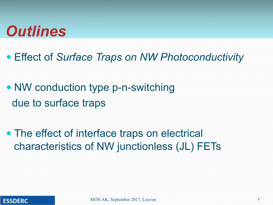
� Effect of Surface Traps on NW Photoconductivity
� NW conduction type p-n-switching due to surface traps � The effect of interface traps on electrical
characteristics of NW junctionless (JL) FETs
MOS-AK, September 2017, Leuven 2
Outlines
ESSDERC
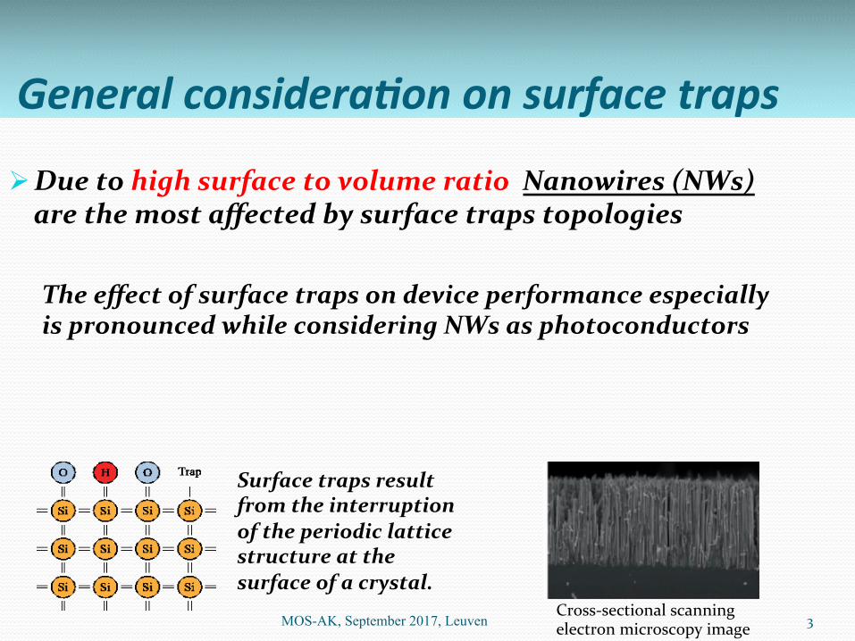
Ø DuetohighsurfacetovolumeratioNanowires(NWs)arethemostaffectedbysurfacetrapstopologies
TheeffectofsurfacetrapsondeviceperformanceespeciallyispronouncedwhileconsideringNWsasphotoconductors
3
Generalconsidera-ononsurfacetraps
Cross-sectionalscanningelectronmicroscopyimageMOS-AK, September 2017, Leuven
Surfacetrapsresultfromtheinterruptionoftheperiodiclatticestructureatthesurfaceofacrystal.
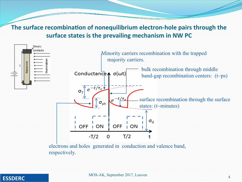
Thesurfacerecombina5onofnonequilibriumelectron-holepairsthroughthesurfacestatesistheprevailingmechanisminNWPC
4MOS-AK, September 2017, Leuven
electrons and holes generated in conduction and valence band, respectively.
Minority carriers recombination with the trapped majority carriers.
bulk recombination through middle band-gap recombination centers: (t~ps)
surface recombination through the surface states: (t~minutes)
ESSDERC
5
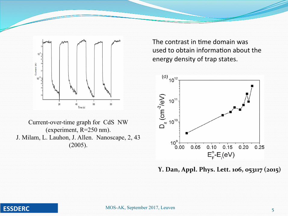
Current-over-time graph for CdS NW (experiment, R=250 nm).
J. Milam, L. Lauhon, J. Allen. Nanoscape, 2, 43 (2005).
Y.Dan,Appl.Phys.Lett.106,053117(2015)
Thecontrastin-medomainwasusedtoobtaininforma-onabouttheenergydensityoftrapstates.
MOS-AK, September 2017, Leuven ESSDERC
6
The model of photoconductivity When the light is on the dynamics of PC is determined by rate equation written for the surface density of electrons ns:
( ) kTE
sCholescapts
sSs
S
etnvsNdtdn
tnNRsvndtdn −
−⎟⎠
⎞⎜⎝
⎛−−= )()()( .
MOS-AK, September 2017, Leuven
S.Petrosyan,A.Yesayan,S.Nersesyan,“Photocurrentrelaxa.onsandgaininsemiconductornanowires,”DOI:10.1117/12.2180885Proc.SPIE,v.9440,2014.
ESSDERC

7
Photocurrent over time graph illustrated in the scale of milliseconds.
Comparison of analytical model and experimental data:
N.A. Stanford, P. T. Blanchard, K.A. Bertness et al. J. Appl. Phys. 107, 034318 (2010).
MOS-AK, September 2017, Leuven
The PC decay after turning the light off. GaNNW
ESSDERC

8MOS-AK, September 2017, Leuven
Conclusion: q Thedevelopedmodelexplainboththedarkconductivityanddynamics
ofPCtransients
q Thekineticsofthephotoconductivityischaracterizedbylong-periodrelaxationprocesses.ThepersistentPCcanbeobservedevenatroomtemperatures
q Atsmallintensitieswecalculateveryhighphotoconductivegain(108-109).GainfollowsaninversepowerlawGn~P-k,wherek=0.9.Alsoonemayexpectthatsuchaultra-highgaincouldallowreachingevensingle-photondetectioninaNWbasedphotoconductor
q SurfacetrapsplaycrucialroleinNWPC!
ESSDERC
� Effect of Surface Traps on NW Photoconductivity
� NW conduction type p-n-switching due to surface traps
� The effect of interface traps on electrical characteristics of NW junctionless (JL) FETs
MOS-AK, September 2017, Leuven 9
Outlines
ESSDERC

Ø Par-allydepleted(onlypartoftheelectronsaretrappedonthesurface)
Ø Fullydepleted(alltheelectronsareremovedfromthevolume)
Ø Inverted(electronsfromvalancebandarecapturedbysurfacetrapsandholesbecomemajority)
10
TheeffectofsurfacetrapsonasingleNWLet’sconsidern-types/cNWandacceptortypesurfacetrapsUpondependingonNWparameters:radius(R),thedopingdensity(ND)andthedensityofsurfacestates(Ns)theNWcanbe:
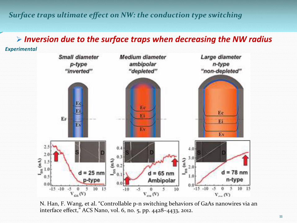
Ø InversionduetothesurfacetrapswhendecreasingtheNWradiusExperimental
11
SurfacetrapsultimateeffectonNW:theconductiontypeswitching
N.Han,F.Wang,etal.“Controllablep-nswitchingbehaviorsofGaAsnanowiresviaaninterfaceeffect,”ACSNano,vol.6,no.5,pp.4428–4433,2012.
12
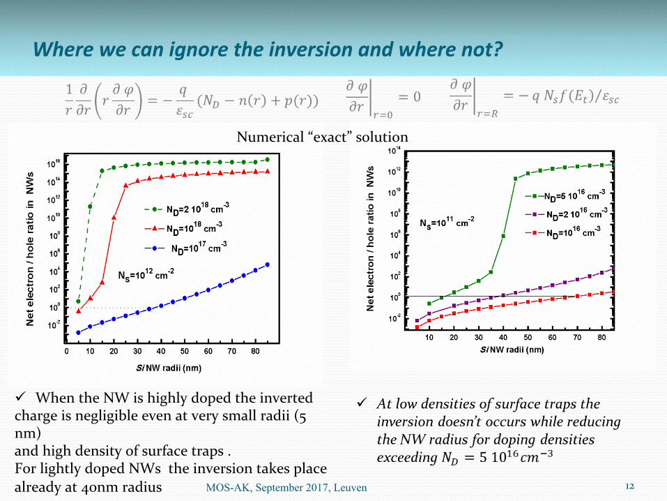
Wherewecanignoretheinversionandwherenot?
Numerical“exact”solution
ü WhentheNWishighlydopedtheinvertedchargeisnegligibleevenatverysmallradii(5nm)andhighdensityofsurfacetraps.ForlightlydopedNWstheinversiontakesplacealreadyat40nmradius MOS-AK, September 2017, Leuven
13
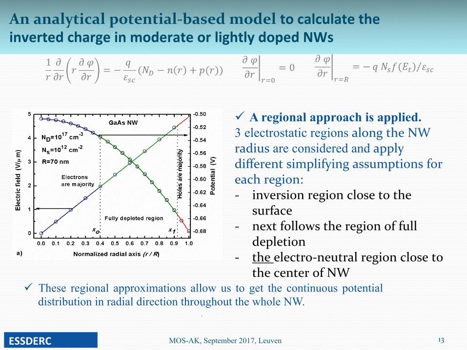
Ananalyticalpotential-basedmodeltocalculatetheinvertedchargeinmoderateorlightlydopedNWs
ü A regional approach is applied. 3 electrostatic regions alongtheNWradiusare considered and applydifferentsimplifyingassumptionsforeachregion:- inversionregionclosetothe
surface- nextfollowstheregionoffull
depletion- theelectro-neutralregioncloseto
thecenterofNWü These regional approximations allow us to get the continuous potential
distribution in radial direction throughout the whole NW. 0x
1x
MOS-AK, September 2017, Leuven ESSDERC
14MOS-AK, September 2017, Leuven
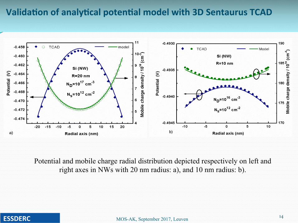
Valida5onofanaly5calpoten5almodelwith3DSentaurusTCAD
Potential and mobile charge radial distribution depicted respectively on left and right axes in NWs with 20 nm radius: a), and 10 nm radius: b).
ESSDERC

15
The dependences of floating (xo, x1) points on NW radii at normalized radial axis: left axis, and at non-normalized axis: the inset
Calcula5onsforNWswithdifferentradii
CentralandsurfacepotentialsforNWswithdifferentradii.Lines:analyticalmodel,circles:numericalcalculations(Wolfram)
MOS-AK, September 2017, Leuven ESSDERC
16
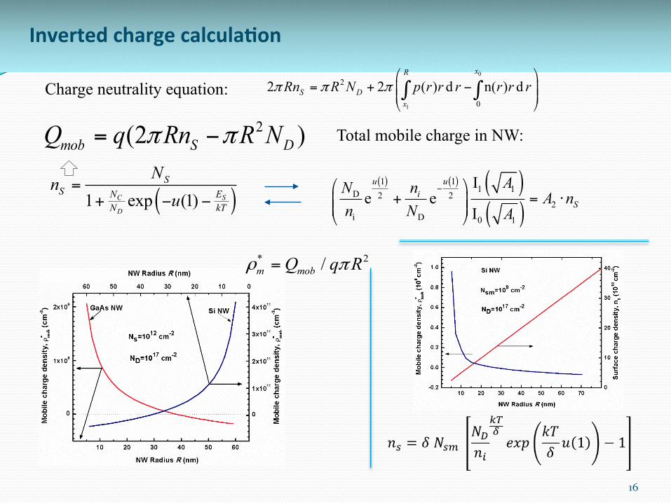
Invertedchargecalcula5on
Charge neutrality equation:0
1
2
0
2 2 ( ) d n( ) dxR
S Dx
Rn R N p r r r r r rπ π π⎛ ⎞
= + −⎜ ⎟⎜ ⎟⎝ ⎠∫ ∫
2(2 )mob S DQ q Rn R Nπ π= − Total mobile charge in NW:
( )1 exp (1)C S
D
SS N E
N kT
Nn
u=
+ − −( ) ( ) ( )
( )1 1
1 1D 2 22
i D 0 1
Ie e
I
u ui
S
AnNn N
A nA
−⎛ ⎞+ = ⋅⎜ ⎟⎜ ⎟
⎝ ⎠
* 2/m mobQ q Rρ π=

17MOS-AK, September 2017, Leuven
Conclusion: q We clarified the conditions when the surface traps
effect can cause inversion in NW. q The potential model was developed including both
type of mobile charges in Poisson equation. q The derived potential model provides a simple way
to calculate the inverted charge density raised due to surface traps effect.
q The model accurately predicts the radius
dependent conductivity type switching in semiconductor NWs which is important for optimal design of nanowire devices.
ESSDERC
� Effect of Surface Traps on NW Photoconductivity
� The ultimate effect of surface traps on NW conduction type, causing p-n-switching, analytical model
� The effect of interface traps on electrical
characteristics of NW junctionless (JL) FETs
MOS-AK, September 2017, Leuven 18
Outlines
ESSDERC

19
q For sensing applications junctionless (JL) FETs are the most used, as there are no junctions along the NW: conducting channel, source and drain have the same doping type and density, which makes easy the fabrication process.
q TheeffectofinterfacetrapsonJLFETcharacteristicswaspresented
HowstrongistheimpactofsurfacetrapsonNWbasedFETs?
A. Yesayan,F.JazaeriandJ.M.Sallese,IEEETransactionsonElectronDevices,vol.63,no.3,pp.1368-1374,March2016.
MOS-AK, September 2017, Leuven ESSDERC
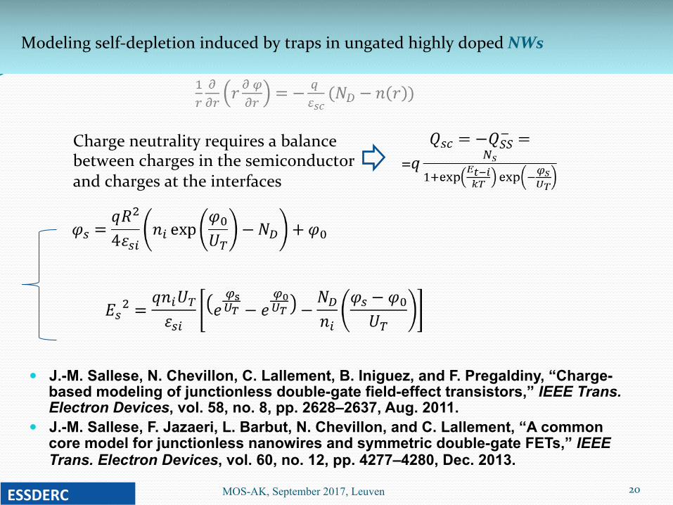
� J.-M. Sallese, N. Chevillon, C. Lallement, B. Iniguez, and F. Pregaldiny, “Charge-based modeling of junctionless double-gate field-effect transistors,” IEEE Trans. Electron Devices, vol. 58, no. 8, pp. 2628–2637, Aug. 2011.
� J.-M. Sallese, F. Jazaeri, L. Barbut, N. Chevillon, and C. Lallement, “A common core model for junctionless nanowires and symmetric double-gate FETs,” IEEE Trans. Electron Devices, vol. 60, no. 12, pp. 4277–4280, Dec. 2013.
20MOS-AK, September 2017, Leuven
Chargeneutralityrequiresabalancebetweenchargesinthesemiconductorandchargesattheinterfaces
Modelingself-depletioninducedbytrapsinungatedhighlydopedNWs
ESSDERC
21
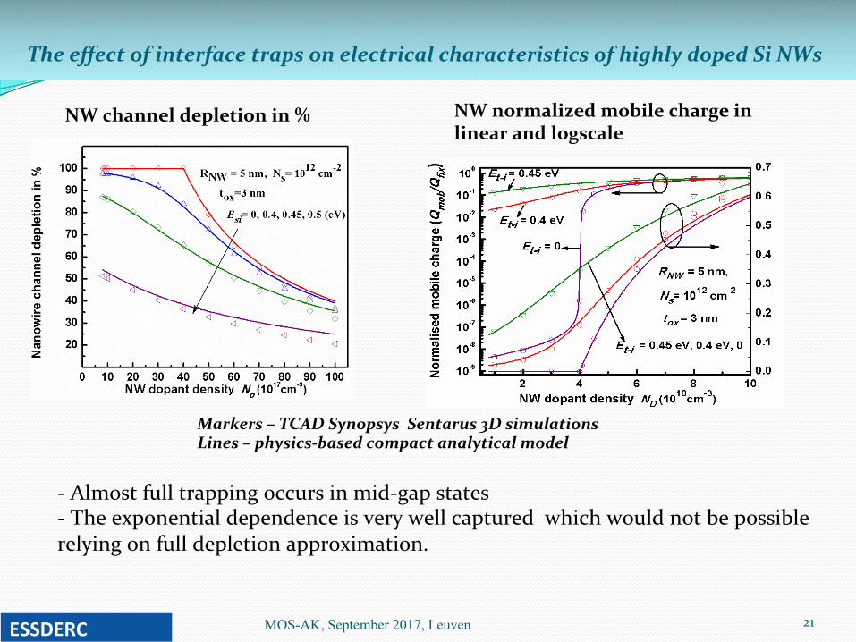
TheeffectofinterfacetrapsonelectricalcharacteristicsofhighlydopedSiNWs
Markers–TCADSynopsysSentarus3DsimulationsLines–physics-basedcompactanalyticalmodel
MOS-AK, September 2017, Leuven
-Almostfulltrappingoccursinmid-gapstates-Theexponentialdependenceisverywellcapturedwhichwouldnotbepossiblerelyingonfulldepletionapproximation.
NWchanneldepletionin% NWnormalizedmobilechargeinlinearandlogscale
ESSDERC

22MOS-AK, September 2017, Leuven
ChargebasedmodelingofNWjunctionlessFETswithinterfacetraps
A. Yesayan,F.Pregaldiny,andJ.-M.Sallese,SolidStateElectron,vol.89,pp.134-138,Nov.2013.
ESSDERC
23
(a)
(b)
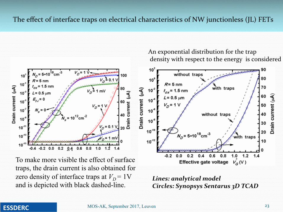
TheeffectofinterfacetrapsonelectricalcharacteristicsofNWjunctionless(JL)FETs
Anexponentialdistributionforthetrapdensitywithrespecttotheenergyisconsidered
Lines:analyticalmodelCircles:SynopsysSentarus3DTCAD
MOS-AK, September 2017, Leuven
To make more visible the effect of surface traps, the drain current is also obtained for zero density of interface traps at VD = 1V and is depicted with black dashed-line.
ESSDERC
Ø Inclusion of surface traps in nanowire topologies has been done on top of a charge-based model developed previously.
Ø Different trap energies and densities were analyzed in detail.
Ø The proposed model reproduces correctly the results obtained from TCAD simulations.
Ø This research represents an interesting development which can be useful for the design of nanowire based biosensors where the free surface is used to sense biological solutions and chemicals.
24
Conclusion
MOS-AK, September 2017, Leuven ESSDERC

Armenia
ESSDERC MOS-AK, September 2017, Leuven

ESSDERC
TechnologiesinArmenia
Mic
ro-a
nd n
ano-
elec
tron
ics
Pho
toni
cs
Adv
ance
d M
ater
ials
Nan
otec
hnol
ogie
s
Bio
tech
nolo
gy
Advanced Manufacturing
Well developed*
Less developed
*) Approximate picture
MOS-AK, September 2017, Leuven

ESSDERC
ITservicesexportIf we look to IT services export chart we see that with this index Armenia is placed at the top of CIS countries.
The chart is provided from World Bank publications 2012.
MOS-AK, September 2017, Leuven
ESSDERC
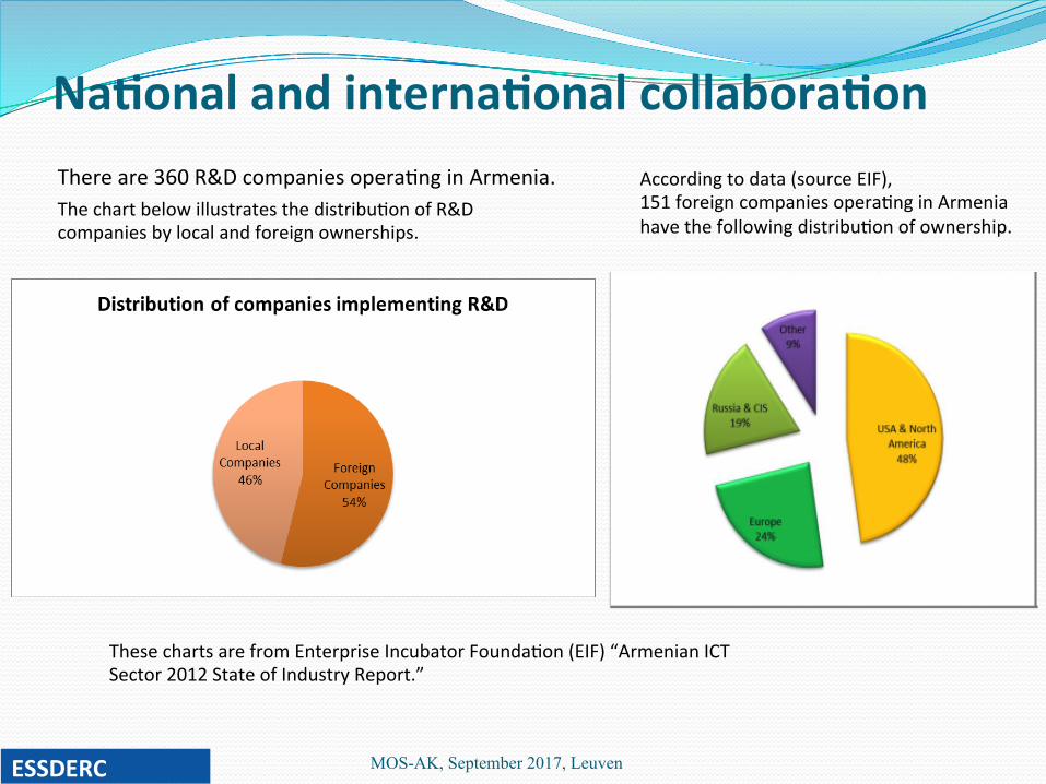
Na5onalandinterna5onalcollabora5on
Thechartbelowillustratesthedistribu-onofR&Dcompaniesbylocalandforeignownerships.
Accordingtodata(sourceEIF),151foreigncompaniesopera-nginArmeniahavethefollowingdistribu-onofownership.
Thereare360R&Dcompaniesopera-nginArmenia.
ThesechartsarefromEnterpriseIncubatorFounda-on(EIF)“ArmenianICTSector2012StateofIndustryReport.”
MOS-AK, September 2017, Leuven
ESSDERC
Usefulllinkstofindmoreaboutthecurrentsitua5oninscienceandac5vi5esofresearchgroups:
Research & Development
• Armenian Journal of Physics: http://ajp.asj-oa.am/ • Journal of Contemporary Physics, Publisher Springer Verlag http://www.springer.com/physics/particle+and+nuclear+physics/journal/11958
• Center of Semiconductor Devices & Nanotechnologies: http://www.semicond.ysu.am/ • State Committee of Science: http://scs.am/?hl=en_US • Armenian Academy of Sciences: http://www.sci.am/index.php?langid=1
Commercial-Technology oriented organizations
• Enterprise Incubator Foundation (EIF): http://www.eif.am/eng • Viasphere Technopark: http://www.viasphere.com/technopark/tenants.htm
• Union of Information Technology Enterprises: http://uite.org/en/projects
MOS-AK, September 2017, Leuven
ESSDERC
• Armenian universities have close cooperation with private businesses. Example of such cooperation is: • Interdepartmental Chairs of “Microelectronic Circuits and Systems” established by Synopsys at SEUA, YSU, RAU since 2004.
Synopsys has the heavy investment in local microelectronics education. Established a presence in Armenia in 2004 Synopsys currently is one of the largest IT employers in Armenia with more than 570 employees.
ü These cooperation of business and high education provides Armenia with highly qualified and industry-ready IT specialists.
Coopera-onofHighEduca-onwithPrivateBusinesses
MOS-AK, September 2017, Leuven
31
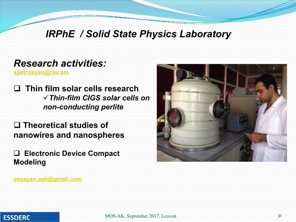
IRPhE / Solid State Physics Laboratory
Research activities: [email protected] q Thin film solar cells research
ü Thin-film CIGS solar cells on non-conducting perlite
q Theoretical studies of nanowires and nanospheres
q Electronic Device Compact Modeling [email protected]
ESSDERC MOS-AK, September 2017, Leuven