Embed Size (px)
Citation preview

Assembly and Operations Manual
Z10000B‐U Buffer Amplifier
Version 1.02 / 23 November 2009
7236 Clifton Road Clifton Virginia 20124
Telephone: (703) 830‐0368 Fax: (703) 830‐0711
http://www.cliftonlaboratories.com

Assembly and Operations Manual
Z10000B‐U
Version 1.02 November 2009
(c) 2006, 2008, 2009 Jack R. Smith d/b/a/ Clifton Laboratories.
Last Revised 23 November 2009
Clifton Laboratories – Z10000B Buffer Amplifier Assembly and Operation Page 1
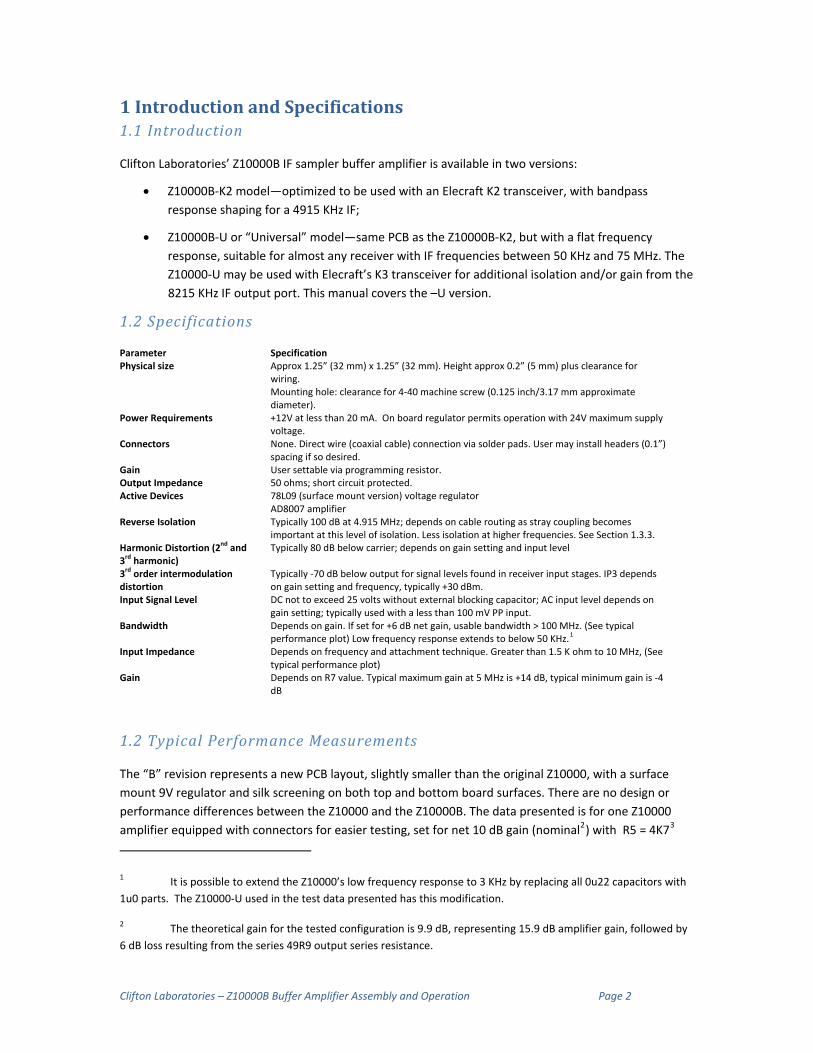
1 Introduction and Specifications 1.1 Introduction
Clifton Laboratories’ Z10000B IF sampler buffer amplifier is available in two versions:
• Z10000B‐K2 model—optimized to be used with an Elecraft K2 transceiver, with bandpass response shaping for a 4915 KHz IF;
• Z10000B‐U or “Universal” model—same PCB as the Z10000B‐K2, but with a flat frequency response, suitable for almost any receiver with IF frequencies between 50 KHz and 75 MHz. The Z10000‐U may be used with Elecraft’s K3 transceiver for additional isolation and/or gain from the 8215 KHz IF output port. This manual covers the –U version.
1.2 Specifications
Parameter SpecificationPhysical size Approx 1.25” (32 mm) x 1.25” (32 mm). Height approx 0.2” (5 mm) plus clearance for
wiring. Mounting hole: clearance for 4‐40 machine screw (0.125 inch/3.17 mm approximate diameter).
Power Requirements +12V at less than 20 mA. On board regulator permits operation with 24V maximum supply voltage.
Connectors None. Direct wire (coaxial cable) connection via solder pads. User may install headers (0.1”) spacing if so desired.
Gain User settable via programming resistor. Output Impedance 50 ohms; short circuit protected.Active Devices 78L09 (surface mount version) voltage regulator
AD8007 amplifier Reverse Isolation Typically 100 dB at 4.915 MHz; depends on cable routing as stray coupling becomes
important at this level of isolation. Less isolation at higher frequencies. See Section 1.3.3. Harmonic Distortion (2nd and 3rd harmonic)
Typically 80 dB below carrier; depends on gain setting and input level
3rd order intermodulation distortion
Typically ‐70 dB below output for signal levels found in receiver input stages. IP3 depends on gain setting and frequency, typically +30 dBm.
Input Signal Level DC not to exceed 25 volts without external blocking capacitor; AC input level depends on gain setting; typically used with a less than 100 mV PP input.
Bandwidth Depends on gain. If set for +6 dB net gain, usable bandwidth > 100 MHz. (See typical performance plot) Low frequency response extends to below 50 KHz.1
Input Impedance Depends on frequency and attachment technique. Greater than 1.5 K ohm to 10 MHz, (See typical performance plot)
Gain Depends on R7 value. Typical maximum gain at 5 MHz is +14 dB, typical minimum gain is ‐4 dB
1.2 Typical Performance Measurements
The “B” revision represents a new PCB layout, slightly smaller than the original Z10000, with a surface mount 9V regulator and silk screening on both top and bottom board surfaces. There are no design or performance differences between the Z10000 and the Z10000B. The data presented is for one Z10000 amplifier equipped with connectors for easier testing, set for net 10 dB gain (nominal2) with R5 = 4K73
1 It is possible to extend the Z10000’s low frequency response to 3 KHz by replacing all 0u22 capacitors with 1u0 parts. The Z10000‐U used in the test data presented has this modification.
2 The theoretical gain for the tested configuration is 9.9 dB, representing 15.9 dB amplifier gain, followed by 6 dB loss resulting from the series 49R9 output series resistance.
Clifton Laboratories – Z10000B Buffer Amplifier Assembly and Operation Page 2

and R7 = 95R3. A 49R9 surface mount resistor was installed across the test amplifier’s input to provide for 50 ohm nominal input impedance.
1.3.1 Frequency Response and Gain
At 5 MHz, the sample unit’s measured gain is 9.78 dB, 0.12 dB less than theoretically predicted. The 3 dB bandwidth extends from 3 KHz to 174 MHz.
1.3.2 Input Impedance
The buffer amplifier’s input impedance is dominated by two elements; the bias isolation resistor (4K7 in the Z10000B‐U’s normal configuration) and shunt capacitance from the PCB traces, connecting wires to the amplifier and the amplifier’s input capacitance.
The measured data presented at the right should be considered as representative of a Z10000B‐U amplifier with short (a two inches / 50 mm) coaxial cable input leads. The bottom line is 0 ohms impedance, with each graticule line 500 ohms. Two inches of typical 50 ohm coaxial cable represents 5.3pF shunt capacitance, with an impedance of 1000 ohms at 30 MHz.
3 This manual uses decimal multiplier notation where the decimal point is replaced by the multiplier. For example, a 49.9 ohm resistor is identified as 49R9 and a 1.00K resistor is identified as 1K00. Likewise, a 1.5uH inductor is identified as 1u5 and a 0.1uF capacitor as 0u1. This notation helps avoid misreading the schematic or text, particularly if the copy quality is poor.
Clifton Laboratories – Z10000B Buffer Amplifier Assembly and Operation Page 3

1.3.3 Reverse Isolation
The buffer amplifier’s reverse isolation is a function of frequency, as illustrated in the amplifier measurements presented at the right. At 8 MHz, the measured sample exhibited 115 dB reverse isolation.
Reverse isolation is affected by how the amplifier is housed, lead dress, shielding, etc. Accordingly, the isolation illustrated at the right may not be achieved in every instance.
1.3.4 Intermodulation Performance
The illustration at the right shows the
output of the test unit with two equal signals (9900 KHz and 10100 KHz) of ‐10 dBm applied to the amplifier input. The amplifier output is 0 dBm (a 3 dB attenuator is applied ahead of the spectrum analyzer in this plot.)
The third order intermodulation product is ‐71.8 dBm down from either tone. With an output based reference (OIP), therefore, the IP3 is thus +35.9 dBm.
Clifton Laboratories – Z10000B Buffer Amplifier Assembly and Operation Page 4

2 Schematic and Circuit Description 2.1 Schematic
2.2 Theory of Operation
2.2.1 Power Supply.
The AD8007 amplifier is rated at an absolute maximum operating voltage of 12V. In order to provide a safety margin, and to decouple the amplifier from the power supply, U2, a three‐terminal fixed regulator, provides a source of stable +9V to U901. C7 and C8 provide additional decoupling. U1, the AD8007 amplifier, obtains its power via the RC decoupling network comprised of R2, C2 and C6.
Since the circuit operates from a single positive power supply, it is necessary to bias U1’s input to approximately V/2. This is accomplished by the 2:1 voltage divider chain of R3/R4. C3 bypasses the V/2 reference voltage; whilst R5 increases U1’s input impedance by isolating C3’s RF ground. R5’s maximum value is determined by the U1’s input bias current on the positive pin, specified by Analog Devices as 8μA. For 4K7, this bias current represents an IR drop of 38 mV. With a DC gain of 4, the corresponding output DC offset will be about 150 mV. If absolutely necessary for high input impedance, R5 may be substituted with a higher value resistor, up to approximately 22K0. However, at frequencies above a few MHz, the
Clifton Laboratories – Z10000B Buffer Amplifier Assembly and Operation Page 5

input impedance is dominated by shunt capacitance; increasing R5 should be done only with an understanding of all the factors affecting the input impedance.4
2.2.2 Amplifier
U1, an Analog Devices AD8007, is a high performance, low noise current feedback amplifier, with a gain‐bandwidth product exceeding 650 MHz. A current feedback amplifier is also known as a “transimpedance” amplifier. Analog Devices describes how a current feedback amplifier works:
First, the negative input of a CFA responds to current; the output voltage is proportional to that current, hence transimpedance (V(out) = Z(t) I(in)). Instead of keeping the negative input current small by maintaining high input impedance, and using feed‐back and voltage gain to keep the input voltage difference small, the CFA keeps the voltage difference small by virtue of its low input impedance (like looking back into a low‐offset emitter follower); and it keeps its net input current small dynamically by feedback from the output.
When an ideal CFA is driven at the high‐impedance positive input, the negative input, with its low impedance, follows closely in voltage; and the high gain for error current and the negative feedback through Rf require that the currents through Rf and Rin be equal; hence V(out) = V(in)[R(f)/R(in) + 1], just like for voltage‐feedback amplifiers. A major difference is that the slew rate can be quite high, because large transient currents can flow in the input stage to handle rapid changes in voltage across the compensating capacitor(s). Also, the low impedance at the negative input means that stray input capacitance will not substantially affect the amplifier's bandwidth.
U1’s gain (in dB) is determined by the ratio of resistors R6 and R7:
776log20 10 R
RRGain +=
R8, 49R9, allows U1 to drive capacitive loads, such as coaxial cable and also protects U1 against operation into short circuits. However, the voltage divider effect of R8, which is in series with the load, reduces the net available gain into a 50 ohm load by 6 dB.
(The K2 version adds a low pass filter, comprised of L1, L2, C10, C11 and C12, to reduce gain above approximately 5 MHz, with C5, C1 and R5 selected to roll off the response below approximately 5 MHz. This combination provides an overall bandpass response shape, reducing unwanted coupling from the K2’s local oscillator coupling into the Z10000‐K2’s output. C1, R5 and R7 have recommended values determined based upon the connection point to the Elecraft K2’s IF circuit.)
2.2.3 Gain Setting in the Z10000B‐U Buffer Amplifier
To vary buffer amplifier’s gain, select R7 using the following table.
4 Clifton Laboratories will provide interested Z10000 owners with the LTSpice model of the AD8007 and an LTSpice model of the amplifier circuits upon request. SPICE modeling will allow the user to determine the effects of component changes with a reasonable degree of accuracy.
Clifton Laboratories – Z10000B Buffer Amplifier Assembly and Operation Page 6

Net Gain (net of R8 series resistance) R7+15 dB 49R9+10 dB 100R+6.7 dB 150R+4.3 dB 221R0 dB 499R‐2.5 dB 1K00‐3.5 dB 1K50‐4.2 dB 2K20
R6 and R1 should not be varied from their design values without a thorough analysis of the circuit.
2.2.4 Values to use with Elecraft K3 Transceiver
When using a Z10000B‐U with an Elecraft K3 transceiver to provide additional gain and isolation over that provided with the K3’s standard IF output port, the following component values should be used:
1. K3’s manufactured prior to August/September 2009 (approximate dates) and with unmodified IF sample circuit. The K3 will exhibit about 15 dB net transfer loss between the antenna port and the IF output port when measured with the K3’s preamplifier off and with a 50 ohm instrument on the IF port. In order to bring the transfer gain to 0 dB, build the Z10000B for 10 db nominal gain. (Approximately 6 dB gain will be added due to the Z10000B’s high input impedance, thereby netting out close to 0 dB transfer gain.) Use the following resistance values: R5: 4K7 R7: 100R
2. K3’s manufactured after August/September 2009 and older K3’s with N8LP’s IF modification. These K3’s have a revised IF output sample circuit with lower transfer loss. Likewise, K3’s manufactured earlier, but with the modification suggested by Larry, N8LP, http://groups.yahoo.com/group/LP‐PAN/files/K3_Buffer_Mod/ will demonstrate about 6‐8 dB transfer loss when measured with the K3’s preamplifier off and with a 50 ohm instrument on the IF port. In order to bring the transfer gain to 0 dB, build the Z10000B for 0 db nominal gain. (Approximately 6 dB gain will be added due to the Z10000B’s high input impedance, thereby netting out at 0 dB transfer gain.) Use the following resistance values: R5: 4K7 R7: 499R
These are recommended values and have proven to be satisfactory for the typical Softrock Lite connection to a K3 and should be used as a starting point.
The Z10000B kit includes extra resistors with these values as well as others for gain setting.
Clifton Laboratories – Z10000B Buffer Amplifier Assembly and Operation Page 7

3 Parts List The Z10000B‐U parts are packaged in a several small envelopes.
• Resistors.
• Capacitors
• Printed circuit board
• Semiconductors (AD8007 amplifier and surface mount 78L09 voltage regulator)
When working with capacitors particularly, do not removed the individual parts from their color‐coded packaging until you are ready to use the component, as their values are not marked on the part and cannot normally be visually distinguished. Hence, if you mix up the capacitors, you will have to measure their values with a capacitance meter.
Do not confuse 100 ohm 1% resistors (identified as 1000) with 1.0K ohm 1% parts, identified as 1001.
Note that the schematic and manual identifies parts with the multiplier as the “decimal” point. For example a 1K ohm resistor is identified as a 1K0, and a 49.9 ohm resistor as 49R9.
Typical Photo Designation Value Marking Qty
C1 0u1 Not marked 1C2 0u01 Not marked 1C3 0u1 Not marked 1C4 0u22 Not marked 1C6 1u0 Not marked 1C5 0u22 Not marked 1C7 0u1 Not marked 1C8 0u1 Not marked 1
R1 200R 2000 1R2 10R 10R0 1R3 1K0 1001 1R4 1K0 1001 1R5 4K7 4701 1R6 499R 4990 1R8 49R9 49R9 1
L1 Zero ohm jumper 000 1
L2 Zero ohm jumper 000 1
Clifton Laboratories – Z10000B Buffer Amplifier Assembly and Operation Page 8

Typical Photo Designation Value Marking Qty
U1 AD8007 AD8007ARZ 1
U2
UA78L09ACPK (or similar)
F9
(plus date code) 1
Gain Setting Parts
See manual Section 2.2.3 and 2.2.4 to determine proper value
Optional Resistor Supplied R5 2K2 2201 1R5 1K1 1101 1R7 49R9 49R9 1R7 100R 1000 1R7 150R 1500 1R7 220R 2200 1R7 499R 4990 1R7 1K0 1001 1R7 1K5 1501 1R7 2K2 2201 1
Z10000B Printed circuit board 1
Multiple part values are provided for R5 and R7, to be selected by the builder as discussed in at Section 2.2.3 and 2.2.4 earlier in this manual.
Printed instructions are not supplied; this manual is to be downloaded from the Clifton Laboratories web site.
Connectors for input, output and power. In most instances, the input, output and power pads will be directly wired into the circuit. However, the pads are spaced for 0.1 inch header pins and if connectors are desired header pins/sockets may easily be installed. Clifton Laboratories will provide, at a small additional charge, a set of three 2‐pin header pins and sockets. These are not part of the standard Z10000.
Clifton Laboratories – Z10000B Buffer Amplifier Assembly and Operation Page 9

4 Assembly 4.1 Orientation
Locate the PCB and orient yourself with the board. Identify the top and bottom.
The left photo is the board top and the right photo is the board bottom.
4.2 Component Installation
Before starting construction, it is necessary to select the gain programming resistor (R7) and the input resistor (R5) as described at Sections 2.2.3 and 2.2.4.
Install the surface mount parts on the top:
Install U1 (AD8007)
Install U2 (F9)
Install C1 0.1 uF unmarked
Install C3 0.1 µF, unmarked
Install C4 0.22 µF, unmarked
Install R1 200 Ω, marked 2000
Install R2 (10 Ω, marked 10R0)
Install R3 1 KΩ, marked 1001
Install R4 1 KΩ, marked 1001
Install R6 499 Ω, marked 4990
Install R8 49.9 Ω, marked 49R9
Clifton Laboratories – Z10000B Buffer Amplifier Assembly and Operation Page 10

Install C5 0.22 µF unmarked
Install C8 0.1 µF, unmarked
Select R5 following instructions at Sections 2.3.3, 2.3.4; Install R5
Select R7 following instructions at Sections 2.3.3, 2.3.4; Install R7
Flip the board upside down and install the remaining surface mount components:
Install C2 0.01 µF, unmarked
Install C6. 1.0 µF, unmarked
Install C7 0.1 µF, unmarked
Install L1 bypass Zero‐ohm jumper marked 000
Install L2 bypass Zero‐ohm jumper marked 000
The two zero‐ohm jumpers are slightly small for the pad spacing but will work if you carefully center the parts on the pads. After soldering one end of each zero ohm jumper in place, check for an inadvertent short to ground. Both ends of both pads should be open circuit to ground when measured with an ohmmeter. Check again after soldering the second end of each zero ohm jumper.
4.3 Checkout
Before applying power, make the following resistance checks. The data presented is taken with a Fluke 189 digital multi‐meter and different meters may provide differing readings. However, any significant variance from these values should be investigated for potential problems. The negative meter lead should be connected to a ground point on the Buffer Amplifier PCB. The test point (TP) Key numbers are depicted in the photograph below, as well as U1’s pins.
Measuring Point TP Key Reading CommentsJ2 (+supply input) 1 100K to
infinite This value may vary considerably from ohmmeter to ohmmeter. Modern low voltage ohms DVM will read 100K to infinity.
J1 input pad 2 infinite Should be infinite to ground as DC is blocked by C1
J3 output pad 3 infinite Should be infinite to ground as DC is blocked by C5.
U1, pin 7 (Vcc) 4 2.0 KΩ Reading dominated by R3/R4 voltage divider impedance.
U1, pin 6 (output) 5 5 MΩ Should be high impedance; hundreds of KΩ at least.
U1, pin 4 (ground) 6 0 ΩU1, pin 3 (+ input) 7 5.9 KΩ This value may vary considerably from
ohmmeter to ohmmeter. U1, pin 2 (‐ input) 8 5 MΩ Should be high impedance; hundreds of
KΩ at least.
Clifton Laboratories – Z10000B Buffer Amplifier Assembly and Operation Page 11

If the Buffer Amplifier meets these measurements, apply +13.8 V DC to the power input, with the negative return to the PCB ground. If possible, use a power supply with current limiting set for 40mA maximum current. Measure the input current. It should be between 10 and 20 mA, and readings significantly over or under these values should be investigated.
5. Troubleshooting The Buffer Amplifier is a simple circuit and there are only two active devices to present problems; the 78L09 voltage regulator, U2 and the AD8007 amplifier, U1.
Faults in U2 can be easily located by measuring the input and output voltage across the regulator. With 13.8 V input, the regulator output should be 9 V ± 0.5 V. If it is above 9 V, the 78L09 is likely defective. If it is below 9 V, then before determining that the 78L09 is defective, the possibility of a short circuit or low impedance load on the regulated output must be first eliminated.
Faults in U1 will normally manifest themselves as reduced gain or reduced signal level output from the Buffer Amplifier. In this case, where the supply and regulated voltages are within range, it may be best to conduct a gain test.
The most common assembly errors reported to date are:
• Confusing the 1000 ohm voltage divider resistors R3 and R4, marked 1001 with the 100 ohm resistor (marked 1000) or the 1100 ohm resistor (marked 1101). If the 100 ohm resistor s inadvertently substituted for either R3 or R4, the DC voltage at U1 Pin 3 will be near 9V or near 1V, depending on which one is improperly installed. If an 1100 ohm resistor is substituted, the DC voltage at U1, Pin 3 will be within 0.5V or so of normal and, in fact, may be left as is if desired.
• Failing to solder one end of a part.
• Solder bridges between adjacent pins of U1.
Clifton Laboratories – Z10000B Buffer Amplifier Assembly and Operation Page 12

5.1 Schematic with Nominal DC Voltage Values
Clifton Laboratories – Z10000B Buffer Amplifier Assembly and Operation Page 13

Clifton Laboratories – Z10000B Buffer Amplifier Assembly and Operation Page 14
Warranty This warranty is effective as of the date of first consumer purchase.
What is covered: During the ninety (90) days after date of purchase, Clifton Laboratories will correct any defects in the Z10000 due to defective parts or, if the Z10000 was assembled by Clifton Laboratories, workmanship, free of charge (post‐paid). You must send the unit at your expense to Clifton Laboratories, but we will pay return shipping. Clifton Laboratories’ warranty does not extend to defects caused by your incorrect assembly or use of unauthorized parts or materials or construction practices.
What is not covered: If the Z10000 is purchased as a kit, this warranty does not cover correction of assembly errors or misalignment; repair of damage caused by misuse, negligence, or builder modifications; or any performance malfunctions involving non‐Clifton Laboratories accessory equipment. The use of acid‐core solder, water‐soluble flux solder, or any corrosive or conductive flux or solvent will void this warranty in its entirety. Whether purchased as an assembled unit or as a kit, also not covered is reimbursement for loss of use, inconvenience, customer assembly or alignment time, or cost of unauthorized service.
Limitation of incidental or consequential damages: This warranty does not extend to non‐Clifton Laboratories equipment or components used in conjunction with our products. Any such repair or replacement is the responsibility of the customer. Clifton Laboratories will not be liable for any special, indirect, incidental or consequential damages, including but not limited to any loss of business or profits.
Under no circumstances is Clifton Laboratories liable for damage to your amateur radio equipment resulting from use of the Z10000, whether in accordance with the instructions in this Manual or otherwise.