Embed Size (px)
Citation preview

DEPARTMENT OF COMPUTER APPLICATIONS COLLEGE OF ENGINEERING,
THIRUVANANTHAPURAM
ASSEMBLY LANGUAGE PROGRAMMING LAB – MANUAL
2005

INDEX CONTENTS PAGE NO 1. The 8085 microprocessor 1
1.1 Introduction 1 1.2 8085 Internal Architecture 1 1.3 8085 Pin Diagram 6 1.4 8085 Addressing Modes 11
2. The 8085 Microprocessor Trainer Kit 12 2.1 Introduction 12 2.2 Specifications of STS -85 VLC 12
2.2.1 Hardware Specifications 13 2.2.2 Software Description 15 3. 8085 Instruction Set Summary 20 4. Entering a program and Execution procedure 24 5. A Sample Program 25 6. 8085 Instructions and Mnemonic codes 26 7. Lab Exercises 28
7.1 Subtract two 8 bit numbers 28 7.2 Divide two 8 bit numbers 29 7.3 Palindrome checking 30 7.4 Sort in ascending order 32 7.5 Sort in descending order 34 7.6 Add two 16 bit numbers 36 7.7 Convert a BCD number to a binary number 38 7.8 Convert a binary number to a BCD number 40 7.9 Add ten 8 bit numbers 41 7.10 Multiply two 8 bit numbers 43 7.11 Largest of ten 8 bit numbers 45 7.12 Smallest of ten 8 bit numbers 47 7.13 Scroll a set of data in memory 49

1. THE 8085 MICROPROCESSOR 1.1 Introduction The 8085 microprocessor was made by Intel in mid 1970s. It was binary compatible with
8080 microprocessor but required less supporting hardware thus leading to less expensive
microprocessor systems. It is a general purpose microprocessor capable of addressing 64k
of memory. The device has 40 pins, require a +5V power supply and can operate with 3
MHz single phase clock. It has also a separate address space for up to 256 I/O ports. The
instruction set is backward compatible with its predecessor 8080 even though they are not
pin-compatible.
1.2 8085 Internal Architecture (Fig: 1)

The 8085 has a 16 bit address bus which enables it to address 64 KB of memory,
a data bus 8 bit wide and control buses that carry essential signals for various operations.
It also has a built in register array which are usually labelled A(Accumulator), B, C, D, E,
H, and L. Further special-purpose registers are the 16-bit Program Counter (PC), Stack
Pointer (SP), and 8-bit flag register F. The microprocessor has three maskable interrupts
(RST 7.5, RST 6.5 and RST 5.5), one Non-Maskable interrupt (TRAP), and one
externally serviced interrupt (INTR). The RST n.5 interrupts refer to actual pins on the
processor a feature which permitted simple systems to avoid the cost of a separate
interrupt controller chip.
Control Unit
Generates signals within microprocessor to carry out the instruction, which has
been decoded. In reality causes certain connections between blocks of the processor be
opened or closed, so that data goes where it is required, and so that ALU operations
occur.
Arithmetic Logic Unit
The ALU performs the actual numerical and logic operation such as ‘add’,
‘subtract’, ‘AND’, ‘OR’, etc. Uses data from memory and from Accumulator to perform
arithmetic and always stores the result of operation in the Accumulator.
Registers
The 8085 microprocessor includes six registers, one accumulator, and one flag
register, as shown in Fig 1. In addition, it has two 16-bit registers: the stack pointer and
the program counter. The 8085 has six general-purpose registers to store 8-bit data; these
are identified as B, C, D, E, H, and L as shown in Fig 1. They can be combined as
register pairs - BC, DE, and HL - to perform some 16-bit operations. The programmer
can use these registers to store or copy data into the registers by using data copy
instructions.

Accumulator
The accumulator is an 8-bit register that is a part of arithmetic/logic unit (ALU).
This register is used to store 8-bit data and to perform arithmetic and logical operations.
The result of an operation is stored in the accumulator. The accumulator is also identified
as register A.
Flag Registers
The ALU includes five flip-flops, which are set or reset after an operation
according to data conditions of the result in the accumulator and other registers. They are
called Zero(Z), Carry (CY), Sign (S), Parity (P), and Auxiliary Carry (AC) flags. The
most commonly used flags are Zero, Carry, and Sign. The microprocessor uses these
flags to test data conditions.
Program Counter (PC)
This 16-bit register deals with sequencing the execution of instructions. This
register is a memory pointer. Memory locations have 16-bit addresses, and that is why
this is a 16-bit register. The microprocessor uses this register to sequence the execution of
the instructions. The function of the program counter is to point to the memory address
from which the next byte is to be fetched. When a byte (machine code) is being fetched,
the program counter is incremented by one to point to the next memory location.
Stack Pointer (SP)
The stack pointer is also a 16-bit register used as a memory pointer. It points to a
memory location in R/W memory, called the stack. The beginning of the stack is defined
by loading 16-bit address in the stack pointer.
Instruction Register / Decoder
This is a temporary store for the current instruction of a program. Latest instruction
is sent to here from memory prior to execution. Decoder then takes instruction and
‘decodes’ or interprets the instruction. Decoded instruction is then passed to next stage.

Memory Address Register (MAR)
Holds addresses received from PC for eg: of next program instruction. MAR feeds
the address bus with address of the location of the program under execution.
Control Generator
Generates signals within microprocessor to carry out the instruction which has
been decoded. In reality it causes certain connections between blocks of the processor to
be opened or closed, so that data goes where it is required, and so that ALU operations
occur.
Register Selector This block controls the use of the register stack. Just a logic circuit which switches
between different registers in the set will receive instructions from Control Unit.
8085 System Bus
The microprocessor performs four operations primarily.
• Memory Read
• Memory Write
• I/O Read
• I/O Write
All these operations are part of the communication processes between microprocessor
and peripheral devices. The 8085 performs these operations using three sets of
communication lines called buses - the address bus, the data bus and the control bus.
Address Bus
The address bus is a group of 16 lines. The address bus is unidirectional: bits flow
only in one direction – from the 8085 to the peripheral devices. The microprocessor uses
the address bus to perform the first function: identifying a peripheral or memory location.
Each peripheral or memory location is identified by a 16 bit address. The 8085 with its 16
lines is capable of addressing 64 K memory locations.

Data Bus
The data bus is a group of eight lines used for dataflow. They are bidirectional: data
flows in both direction between the 8085 and memory and peripheral devices. The 8 lines
enable the microprocessor to manipulate 8-bit data ranging from 00 to FF.
Control Bus
The control bus consists of various single lines that carry synchronization signals.
These are not groups of lines like address of data bus but individual lines that provide a
pulse to indicate an operation. The 8085 generates specific control signal for each
operation it performs. These signals are used to identify a device type which the
processor intends to communicate.

1.3 8085 Pin Diagram (Fig: 2)

8085 Pin Description
Properties Single + 5V Supply 4 Vectored Interrupts (One is Non Maskable) Serial In/Serial Out Port Decimal, Binary, and Double Precision Arithmetic Direct Addressing Capability to 64K bytes of memory
A6-A1 (Output 3 states)
Address Bus; The most significant 8 bits of the memory address or the 8 bits of the
I/0 address; 3 stated during Hold and Halt modes.
AD0 - 7 (Input/Output 3state)
Multiplexed Address/Data Bus; Lower 8 bits of the memory address (or I/0
address) appear on the bus during the first clock cycle of a machine state. It then becomes
the data bus during the second and third clock cycles. 3 stated during Hold and Halt
modes.
ALE (Output)
Address Latch Enable: It occurs during the first clock cycle of a machine state and
enables the address to get latched into the on chip latch of peripherals. The falling edge of
ALE is set to guarantee setup and hold times for the address information. ALE can also
be used to strobe the status information. ALE is never 3 stated.
SO, S1 (Output)
Data Bus Status: Encoded status of the bus cycle:
S1 S0
0 0 HALT
0 1 WRITE
1 0 READ
1 1 FETCH
S1 can be used as an advanced R/W status.
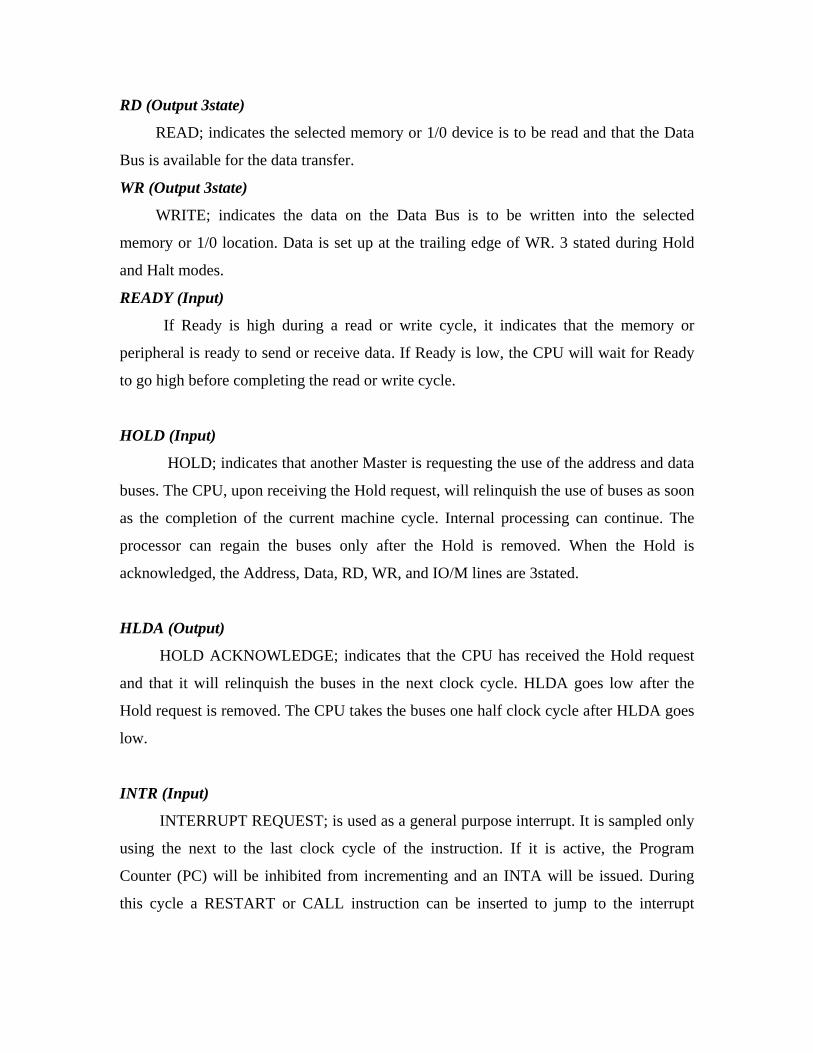
RD (Output 3state)
READ; indicates the selected memory or 1/0 device is to be read and that the Data
Bus is available for the data transfer.
WR (Output 3state)
WRITE; indicates the data on the Data Bus is to be written into the selected
memory or 1/0 location. Data is set up at the trailing edge of WR. 3 stated during Hold
and Halt modes.
READY (Input)
If Ready is high during a read or write cycle, it indicates that the memory or
peripheral is ready to send or receive data. If Ready is low, the CPU will wait for Ready
to go high before completing the read or write cycle.
HOLD (Input)
HOLD; indicates that another Master is requesting the use of the address and data
buses. The CPU, upon receiving the Hold request, will relinquish the use of buses as soon
as the completion of the current machine cycle. Internal processing can continue. The
processor can regain the buses only after the Hold is removed. When the Hold is
acknowledged, the Address, Data, RD, WR, and IO/M lines are 3stated.
HLDA (Output)
HOLD ACKNOWLEDGE; indicates that the CPU has received the Hold request
and that it will relinquish the buses in the next clock cycle. HLDA goes low after the
Hold request is removed. The CPU takes the buses one half clock cycle after HLDA goes
low.
INTR (Input)
INTERRUPT REQUEST; is used as a general purpose interrupt. It is sampled only
using the next to the last clock cycle of the instruction. If it is active, the Program
Counter (PC) will be inhibited from incrementing and an INTA will be issued. During
this cycle a RESTART or CALL instruction can be inserted to jump to the interrupt

service routine. The INTR is enabled and disabled by software. It is disabled by Reset
and immediately after an interrupt is accepted.
INTA (Output)
INTERRUPT ACKNOWLEDGE; is used instead of (and has the same timing
as) RD during the Instruction cycle after an INTR is accepted. It can be used to activate
the 8259 Interrupt chip or some other interrupt port.
RST 5.5
RST 6.5 - (Inputs)
RST 7.5
RESTART INTERRUPTS; These three inputs have the same timing as I NTR except
they cause an internal RESTART to be automatically inserted.
RST 7.5 ~~ Highest Priority
RST 6.5
RST 5.5 o Lowest Priority
The priority of these interrupts is ordered as shown above. These interrupts have a higher
priority than the INTR.
TRAP (Input)
Trap interrupt is a nonmaskable restart interrupt. It is recognized at the same
time as INTR. It is unaffected by any mask or Interrupt Enable. It has the highest priority
of any interrupt.
RESET IN (Input)
Reset sets the Program Counter to zero and resets the Interrupt Enable and
HLDA flipflops. None of the other flags or registers (except the instruction register) are
affected The CPU is held in the reset condition as long as Reset is applied.
RESET OUT (Output)
Indicates CPlJ is being reset. Can be used as a system RESET. The signal is synchronized
to the processor clock.

X1, X2 (Input)
Crystal or R/C network connections to set the internal clock generator X1 can also be an
external clock input instead of a crystal. The input frequency is divided by 2 to give the
internal operating frequency.
CLK (Output)
Clock Output for use as a system clock when a crystal or R/ C network is used
as an input to the CPU. The period of CLK is twice the X1, X2 input period.
IO/M (Output)
IO/M indicates whether the Read/Write is to memory or l/O Tristated during
Hold and Halt modes.
SID (Input)
Serial input data line: The data on this line is loaded into accumulator bit 7
whenever a RIM instruction is executed.
SOD (output)
Serial output data line: The output SOD is set or reset as specified by the SIM
instruction.
Vcc
+5 volt supply.
Vss
Ground Reference

1.4 8085 Addressing modes
They are mainly classified into four:
Immediate addressing.
Register addressing.
Direct addressing.
Indirect addressing.
Immediate addressing
Data is present in the instruction. Load the immediate data to the destination provided.
Example: MVI R,data
Register addressing
Data is provided through the registers.
Example: MOV Rd, Rs
Direct addressing
Used to accept data from outside devices to store in the accumulator or send the data
stored in the accumulator to the outside device. Accept the data from the port 00H and
store them into the accumulator or Send the data from the accumulator to the port 01H.
Example: IN 00H or OUT 01H
Indirect Addressing
This means that the Effective Address is calculated by the processor and the contents of
the address (and the one following) are used to form a second address. The second
address is where the data is stored. Note that this requires several memory accesses; two
accesses to retrieve the 16-bit address and a further access (or accesses) to retrieve the
data which is to be loaded into the register.

2. The 8085 MICROPROCESSOR TRAINER KIT 2.1 Introduction From the 4 bit microprocessor brought out by Intel in 1971,advancement in technology have been made and now 8 bit ,16 bit , 32 bit and 64 bit microprocessors are available and 64 bit and 32 bit microprocessors are dominating the market. From the age of vacuum tubes and transistors, we are now in the age of microprocessors. Due to its adoptability and intelligence, they are used extensively. The trainer kit is a low cost 8085 based training tool developed specifically for learning the operation of today's microprocessor based systems. The purpose of a microprocessor trainer kit is to:
Facilitate people in learning and using machine code programming. Familiarise people of the basic microprocessor hardware. Facilitate testing of hand coded programs with the help of break point setting. Facilitate easy interface to external I/O devices. Facilitate training with its peripherals also.
STS-85 is a low cost microprocessor trainer kit and it is based on the most popular 8 bit microprocessor INTEL 8085. It has 6 digits of seven segment display and 24 keys keyboard. STS – 85 VLC is supplied with minimum basic hardware required to function as a trainer. User can add additional memory on board. 2.2 Specifications of STS -85 VLC The specifications of STS-85 VLC low cost 8085 microprocessor trainer kit are: Hardware CPU : 8085A with 3.579545 MHz/ 4.000MHz/6.144Mhz with no wait states. Memory : 8 k EPROM (2764) 8 K RAM (6264) 2 Expansion socket space. Key board : 24 keys keyboard Display : 6 digit bright seven segment display Peripherals Used : 8279 , 8255 for user Terminations : The data, address and control lines and programmable I/O lines of the peripherals are terminated in different connectors.

Software (a) Program entry
• Address field is 4 digits wide for the 16 bit address of 8085A. Data field is 2 digits wide for 8 bit data of 8085A.
• Set address and verify the contents of present location. • Data is set altered in memory immediately for each hex key entry. • Automatic setting of RAM starts address on pressing INR or DCR key. • Increment/decrement the address and display /alter the data contents.
(b) Program execution
• Program could be executed from any address using GO key with or without break point. User can use the display routine available in the monitor to display their data.
• Execution with break point with break count facility for easy software debugging.
• Facility to display/edit the registers of user registers saved while break. (c) Program editing
• Move block of data in the RAM. • Fill block of memory with constant data in the RAM. • Facility to alter any location of RAM in data set mode.
(c) Miscellaneous
• Memory test facility for RAM. • Check sum facility for ROM in the same memory test function.
2.2.1 Hardware Specifications The main CPU PCB has the facility to accommodate one 8255A (programmable peripheral interface), one 8279 (key board display controller) and 4 numbers 28 pin memory IC sockets. It has facility to terminate data, address and control signals on different connectors. 26 pins FRC connector is provided for using 8255 ports by the user for performing experiments with interface boards. STS-85-VLC require a single 5 volts supply for its operation.

8085A CPU STS-85-VLC is based on Intel’s 8 bit microprocessor 8085A. It has a crystal connected to it with a frequency as specified under specifications. The READY line of the CPU is pulled up to operate the CPU without any wait states. Display refreshing and keyboard debouncing are performed in hardware by onboard 8279 IC. The lower order address bus is derived from an octal latch using ALE (Address Latch Enable) signal of 8085A. The data, higher order address and control buses are terminated in various connector points. Memory and I/O Decoding At power on or reset 8085A address bus has an address of 0000H and hence the memory has been so decoded to have EPROM address 0000H to 1FFF-H (2764) . The user RAM address is 8000Hto 9EFF-H. STS-85-VLC is using single decoder IC for memory and I/O. STS-85-VLC is using single decoder IC for memory and I/O. STS-85-VLC when supplied has 16K chip selects. The socket next to monitor EPROM can accommodate another RAM. 74LS 138 next to 8085A acts as decoder. Out of 8 of its outputs 4 are used for memory decoding and other 4 are used for I/O decoding. As only 2 I/O chips are used in the system other 2 decoded I/O chip selects are available for the user. Keyboard and display The keyboard of STS-85-VLC consists of 24 keys and out of which 23 keys are scanned by 8279. RESET key is connected to CPU reset through standard RC network 16 keys are devoted for hexadecimal data entry and the rest are function keys. The display of STS-85-VLC is 6 digit common anode display. Left most 4 digits of the display represents the address and right most 2 digits represents the data at the displayed address. One 8279 (keyboard display controlled) is used for display refresh and keyboard scanning purposes. 74LS138 decoder drives digit driver transistors on display board to refresh display. The scanning and debounce for a key closure is done by 8279 and it uses another 74LS138 decoder to decode the scan lines. The interrupt output of 8279 is connected to RST 7.5 input of 8085A CPU.
Port lines One number 8255A (programmable peripheral interface) is provided on board. All the 24 port lines are terminated on 26 pin FRC connector along with VCC and GND. Port line PC7 is connected to TRAP of 8085 A CPU for future use. The system will function without this IC also. Power Supply Power supply for the trainer is inbuilt / provided externally as required by user. Only logic supply is provided.

Enhanced STS-85 VLC features In enhanced model of STS-85-VLC battery backup circuit and one 8155 (timer, RAM, I/O) IC is available. The RAM of 8155 is not accessible as the chip select input is given from I/O decoder IC. The ‘timer in’ is from processor ‘clock out’ and ‘timer out’ goes to 8085 RST 7.5 input. The existing track from 8279 ‘intr’ has already been disconnected. The port address of various peripheral ICs are a. 8255- 00 to 03 b. 8279- 88H to 89H c. 8155- 0F0H to 0F5H 2.2.2 Software description STS-85-VLC has monitor software which controls the keyboard and display function. The software facilities available in STS-85-VLC include Address set, Increment, Decrement, Data set, Break set, Break clear, Move, Fill, Go(Execute) with and without break, Memory test and Register display/alter functions. System Initialization At ‘power on’ or at manual reset 8085A starts executing the program loaded in 0000H which is the starting address of the monitor EPROM. At this start address the monitor software performs initialization of the microprocessor stack pointer, monitor software flags, control/command registers of 8279 for refreshing the display & scanning the keyboard. Then, the display is written to display the power on prompt one character after the other. After completing initialization, the system waits for a keyboard entry and is ready to receive address or function commands. All the hexadecimal keys are entered into the address field. To enter the data mode, increment (INR) or decrement (DCR) keys should be pressed. Address set and alter the contents On ‘power on’ or manual reset, STS-85 is displayed. Now to set an address use the hexadecimal keys. Hex key entered is placed in the right most column of the address field after scrolling the existing entry and data at that address is displayed. You will be entering keys in the address filed only, until you press INR or DCR key. Once you press this, then the hex keys entered will change the data field and also update the memory contents immediately.

Increment/Decrement In data set mode, the function of INR/CDR key is to increment/decrement the address field and update the display with the corresponding data. In address set mode INR/DCR key should be pressed to enter into data set mode. In data set mode, hex keys are entered in the data field of the display and corresponding memory location is updated automatically. Hex key entered is entered as LSD (least significant digit) in the respective field after scrolling the field left by one digit. Display/Alter CPU Registers You can display and alter the user register values by entering REG mode by pressing REG key, you enter REG mode. Data in the register pair 551FAF. name of the register pair The dot refers to the register under alteration. Now, if you want to change F, Enter the new value and the user save area is updated automatically. To go to next register use INR key and the dot shifts over to A and A value can be altered. One more INR will display BC register in the same way. The display format is the same for DE and HL registers. Next register in the sequence is PC and the display format is as shown below. 8000PC For PC and SP display the dot is having no relevance as they are 16 bit registers and to alter the register value, required hex keys are entered. There is no necessity for using INR key for transferring the displayed data into user save area. Also, by continuously pressing INR/DCR key, you will be looping around in the register mode only. The REG key is of toggle type and by pressing it in REG mode, the system enters the power on prompt. Execute/RAM test and Checksum A program entered in RAM could be executed by pressing GO key. When this key is pressed, the display is as shown below Go Fn And within short time comes back and displays user PC as, 8000 ch. This means that the present user PC value is 8000H and this is to be checked or changed. If the user program starting address is different it could be entered. After entering the correct PC value, INR key is depressed. When this is done, the monitor desaves all the user registers and then the program jumps to user program. MTEST is the alternate function of GO key. The purpose of this key is to perform non destructive memory test for RAM and display the result. For ROM, the checksum from start to end
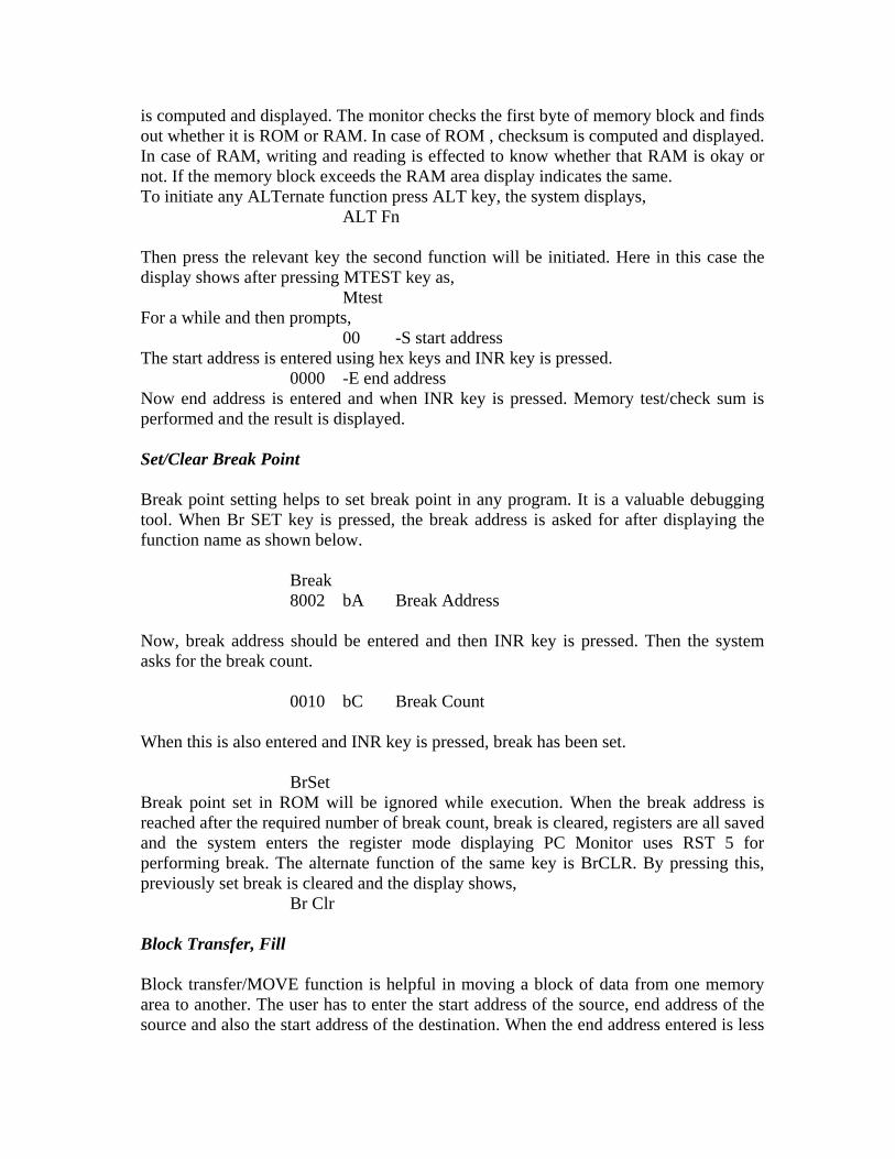
is computed and displayed. The monitor checks the first byte of memory block and finds out whether it is ROM or RAM. In case of ROM , checksum is computed and displayed. In case of RAM, writing and reading is effected to know whether that RAM is okay or not. If the memory block exceeds the RAM area display indicates the same. To initiate any ALTernate function press ALT key, the system displays, ALT Fn Then press the relevant key the second function will be initiated. Here in this case the display shows after pressing MTEST key as, Mtest For a while and then prompts, 00 -S start address The start address is entered using hex keys and INR key is pressed. 0000 -E end address Now end address is entered and when INR key is pressed. Memory test/check sum is performed and the result is displayed. Set/Clear Break Point Break point setting helps to set break point in any program. It is a valuable debugging tool. When Br SET key is pressed, the break address is asked for after displaying the function name as shown below. Break 8002 bA Break Address Now, break address should be entered and then INR key is pressed. Then the system asks for the break count. 0010 bC Break Count When this is also entered and INR key is pressed, break has been set. BrSet Break point set in ROM will be ignored while execution. When the break address is reached after the required number of break count, break is cleared, registers are all saved and the system enters the register mode displaying PC Monitor uses RST 5 for performing break. The alternate function of the same key is BrCLR. By pressing this, previously set break is cleared and the display shows, Br Clr Block Transfer, Fill Block transfer/MOVE function is helpful in moving a block of data from one memory area to another. The user has to enter the start address of the source, end address of the source and also the start address of the destination. When the end address entered is less

than the start address the system does not accept the end address when INR key is pressed. The system proceeds further when the end address is greater than start address. When MOVE is pressed, the system displays MoveFn For a while and then displays, 0000 -S start address The start address is entered using hex keys and INR key is pressed. 0000 -E end address Now end address is entered and when INR key is pressed, the destination address is displayed 0000 -d destination address The destination address if required could be changed and when INR key is pressed ‘move’ function is executed. While entering destination start address, the user can verify and alter start and end addresses of source by pressing DCR key without affecting any values. The ‘move’ function takes care of overlapping memories and moves properly. FILL is the alternate function of MOVE key. This function is for filling an area of RAM with specified data. On pressing this key, prompt for fill is displayed. The starting address, end address and data to be filled are asked for and accepted. When ROM area is tried to be filled it stops there indicating the same. Fill Fn For a while and then displays, 8000 -S Start address 8200 -E End address Data -3E Fill data When INR is pressed after entering fill data, the fill function is executed and the system enters the power on mode. Enhanced STS-85-VLC feature. In enhanced model of STS-85-VLC one additional software function is provided namely, ‘single step’. This is alternate function of REG key. This function is same as that of ‘GO’ key. Here instead of executing user program continuously only one instruction of user program is executed and the system returns to ‘REG’ mode in monitor displaying next instruction address. User registers are desaved before executing the user program and are saved after executing the user program one instruction pointed by the ‘PC’ register content. Set the registers including PC as per your requirement. Press ALT key. Then press REG/STEP key. To proceed to next step press REG/STEP key again. Utilities Commonly used utilities are given under RST instruction, the single byte call instruction for quick reference and ease of use

RST 0 : Return to monitor RST 1 : Scans keyboard until a key is received. The key value is returned in Accumulator and also in B register. RST 2 : One scan of keyboard. If zero flag is set no key is pressed. Otherwise key value is available in accumulator and B register. RST 3 : Display the data available in the display buffer 9F00 (MSD) to 9F05(LSD). The data is put on display after converting through segment table. MS bit is placed onto decimal points. Other 7 bits map to segment table. 00 to 0F in display buffer is displayed as 0 to F on display. 10H onwards it continues with G, H, I…and so on. Power ON location : 9F09/9F0A make this ‘zero’ to restore power on default values including user stack pointer. User delay location : 9F37 (default value 5): If prompt messages are retaining for long or vanishing fast, set this to default value and press Reset Important : Registers display will have user program register value only after a break or single step. If you want to view registers set your break point there (Break address should be beginning address of and instruction) and execute from beginning. Program should stop at the set break point to view registers.

3. 8085 INSTRUCTION SET SUMMARY Mnemonic Description Clock Cycles
• MOVE, LOAD, AND STORE MOV r1 r2 Move register to register 4 MOV M r Move register to memory 7 MOV r M Move memory to register 7 MVI r Move immediate register 7 MVI M Move immediate memory 10 LXI B Load immediate register Pair B & C 10 LXI D Load immediate register Pair D & E 10 LXI H Load immediate register Pair H & L 10 LXI SP Load immediate stack pointer 10 STAX B Store A indirect 7 STAX D Store A indirect 7 LDAX B Load A indirect 7 LDAX D Load A indirect 7 STA Store A direct 13 LDA Load A direct 13 SHLD Store H & L direct 16 LHLD Load H & L direct 16 XCHG Exchange D & E H & L registers 4
• STACK OPS PUSH B Push register Pair B & C on stack 12 PUSH D Push register Pair D & E on stack 12 PUSH H Push register Pair H & L on stack 12 PUSH PSW Push A and Flags on stack 12 POP B Pop register Pair B & C off stack 10 POP D Pop register Pair D & E off stack 10 POP H Pop register Pair H & L off stack 10 POP PSW Pop A and Flags off stack 10 XTHL Exchange top of stack H & L 16 SPHL H & L to stack pointer 6 JUMP JMP Jump unconditional 10 JC Jump on carry 7/10 JNC Jump on no carry 7/10 JZ Jump on zero 7/10 JNZ Jump on no zero 7/10 JP Jump on positive 7/10

JM Jump on minus 7/10 JPE Jump on parity even 7/10 JPO Jump on parity odd 7/10 PCHL H & L to program counter 6 CALL CALL Call unconditional 18 CC Call on carry 9/18 CNC Call on no carry 9/18 CZ Call on zero 9/18 CNZ Call on no zero 9/18 CP Call on positive 9/18 CM Call on minus 9/18 CPE Call on parity even 9/18 CPO Call on parity odd 9/18
• RETURN RET Return 10 RC Return on carry 6/12 RNC Return on no carry 6/12 RZ Return on zero 6/12 RNZ Return on no zero 6/12 RP Return on positive 6/12 RM Return on minus 6/12 RPE Return on parity even 6/12 RPO Return on parity odd 6/12 RESTART RST Restart 12
• INPUT/OUTPUT
IN Input 10 OUT Output 10
• INCREMENT AND DECREMENT INR r Increment register 4 DCR r Decrement register 4 INR M Increment memory 10 DCR M Decrement memory 10 INX B Increment B & C registers 6 INX D Increment D & E registers 6 INX H Increment H & L registers 6 INX SP Increment stack pointer 6 DCX B Decrement B & C 6
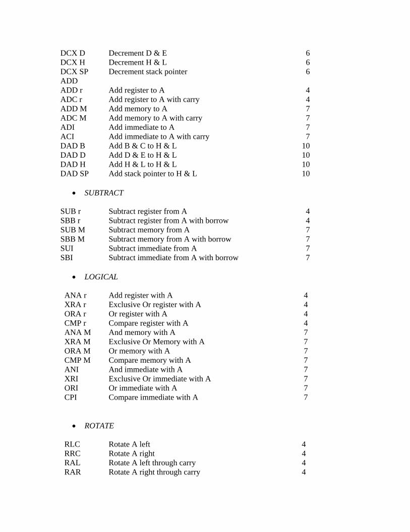
DCX D Decrement D & E 6 DCX H Decrement H & L 6 DCX SP Decrement stack pointer 6 ADD ADD r Add register to A 4 ADC r Add register to A with carry 4 ADD M Add memory to A 7 ADC M Add memory to A with carry 7 ADI Add immediate to A 7 ACI Add immediate to A with carry 7 DAD B Add B & C to H & L 10 DAD D Add D & E to H & L 10 DAD H Add H & L to H & L 10 DAD SP Add stack pointer to H & L 10
• SUBTRACT
SUB r Subtract register from A 4 SBB r Subtract register from A with borrow 4 SUB M Subtract memory from A 7 SBB M Subtract memory from A with borrow 7 SUI Subtract immediate from A 7 SBI Subtract immediate from A with borrow 7
• LOGICAL
ANA r Add register with A 4 XRA r Exclusive Or register with A 4 ORA r Or register with A 4 CMP r Compare register with A 4 ANA M And memory with A 7 XRA M Exclusive Or Memory with A 7 ORA M Or memory with A 7 CMP M Compare memory with A 7 ANI And immediate with A 7 XRI Exclusive Or immediate with A 7 ORI Or immediate with A 7 CPI Compare immediate with A 7
• ROTATE RLC Rotate A left 4 RRC Rotate A right 4 RAL Rotate A left through carry 4 RAR Rotate A right through carry 4

• SPECIALS
CMA Complement A 4 STC Set carry 4 CMC Complement carry 4 DAA Decimal adjust A 4
• CONTROL
EI Enable Interrupts 4 DI Disable Interrupts 4 NOP No-operation 4 HLT Halt (Power down) 5 RIM Read Interrupt Mask 4 SIM Set Interrupt Mask 4

4. ENTERING A PROGRAM AND EXECUTION PROCEDURE After connecting it to the power supply, STS-85 prompt appears. Now press INR. Address field shows 8000 and directly you can start entering data corresponding to first address. Note: In case you select any other starting address, say 8050, then after entering 8050 press INR then only system changes from address field to data field. -Press INR, the address shifts to 8001. -Feed 2nd data and then INR and so on. On completion of the programs, press INR. Execution procedure: - Press GO - System shows some address and ‘Ch’ in data field. - Now select the starting address of the program which is stored for execution say 8000 - After entering the starting address press INR - The program will be executed. Note: In case of addition of two BCD numbers after pressing INR, the initial prompt appears. To refer the output result goes to the address field specified in the program (say 8051). There you can see the added result. For other programs like binding display etc you can see the display blinking directly.

5. A SAMPLE PROGRAM
Aim: To multiply two 8 bit numbers. Program Analysis: Two 8 bit numbers are stored in memory locations 8100 and 8101. They are multiplied and the results are stored in memory locations 8200 and 8201. Program:
Memory address
Machine code
Label Opcode Operand Comments
8000 AF XRA A Clear A 8001 A8 XRA B Clear B 8002 A9 XRA C Clear C 8003 21 LXI H 8100 8004 00 8005 81
Set HL pair as an index to source memory
8006 46 MOV B, M Move [M] to B 8007 23 INX H Increment HL pair 8008 86 L2 ADD M Add [A] to [M] 8009 D2 JNC L1 800A 0D 800B 80
Jump if no carry to L1
800C 0C INR C Increment [C] 800D 05 L1 DCR B Decrement [B] 800E C2 JNZ L2 800F 08 8010 80
Jump if nonzero to L2
8011 32 STA 8200 8012 00 8013 82
Store [A] in 8200
8014 79 MOV A, C Move [C] to A 8015 32 STA 8201 8016 01 8017 82
Store [A] in memory location 8201
8018 76 HLT Stop program
Result: The program is executed and the results are stored in the memory locations 8200 and 8201. Input: At 8100 :03 At 8101 :02 Output:At 8200 : 06 At 8201 : 00

6. 8085 INSTRUCTIONS AND MNEMONIC CODES
Hex mnemonic Hex mnemonic Hex mnemonic Hex mnemonic CE ACI 8-Bit 8F ADC A 88 ADC B 89 ADC C 8A ADC D 8B ADC E 8C ADC H 8D ADC L 8E ADC M 87 ADD A 80 ADD B 81 ADD C 82 ADD D 83 ADD E 84 ADD H 85 ADD L 86 ADD M C6 ADI 8-Bit A7 ANA A A0 ANA B A1 ANA C A2 ANA D A3 ANA E A4 ANA H A5 ANA L A6 ANA M E6 ANA 8-Bit CD CALL 16-Bit DC CC 16-Bit FC CM 16-Bit 2F CMA
3F CMC BF CMP A B8 CMP B B9 CMP C BA CMP D BB CMP E BC CMP H BD CMP BE CMP M D4 CNC 16-Bit C4 CNZ 16-Bit F4 CP 16-Bit EC CPE 16-Bit FE CPI 8-Bit E4 CPO 16-Bit CC CZ 16-Bit 27 DAA 09 DAD B 19 DAD D 29 DAD H 39 DAD SP 3D DCR A 05 DCR B 0D DCR C 15 DCR D 1D DCR E 25 DCR H 2D DCR L 35 DCR M 0B DCX B 1B DCX D
2B DCX H 3B DCX SP F3 DI FB EI 76 HLT DB IN 8-Bit 3C INR A 04 INR B 0C INR C 14 INR D 1C INR E 24 INR H 2C INR L 34 INR M 03 INX B 13 INX D 23 INX H 33 INX SP DA JC 16-Bit FA JM 16-Bit C3 JMP 16-Bit D2 JNC 16-Bit C2 JNC 16-Bit F2 JP 16-Bit EA JPE 16-Bit E2 JPO 16-Bit CA JZ 16-Bit 3A LDA 16-Bit 0A LDAX B 1A LDAX D 2A LHLD 16-Bit
01 LXI B,16-Bit 11 LXI D,16-Bit 21 LXI H,16-Bit 31 LXI SP,16-Bit 7F MOV A A 78 MOV A B 79 MOV A C 7A MOV A D 7B MOV A E 7C MOV A H 7D MOV A L 7E MOV A M 47 MOV B A 40 MOV B B 41 MOV B C 42 MOV B D 43 MOV B E 44 MOV B H 45 MOV B L 46 MOV B M 4F MOV C A 48 MOV C B 49 MOV C C 4A MOV C D 4B MOV C E 4C MOV C H 4D MOV C L 4E MOV C M 57 MOV D A 50 MOV D B 51 MOV D C

Hex mnemonic Hex mnemonic Hex mnemonic Hex mnemonic 52 MOV D D 53 MOV D E 54 MOV D H 55 MOV D L 56 MOV D M 5F MOV E A 58 MOV E B 59 MOV E C 5A MOV E D 5B MOV E E 5C MOV E H 5D MOV E L 5E MOV E M 67 MOV H A 60 MOV H B 61 MOV H C 62 MOV H D 63 MOV H E 64 MOV H H 65 MOV H L 66 MOV H M 6F MOV L A 68 MOV L B 69 MOV L C 6A MOV L D 6B MOV L E 6C MOV L H 6D MOV L L 6E MOV L M 77 MOV M A 70 MOV M B
71 MOV M C 72 MOV M D 73 MOV M E 74 MOV M H 75 MOV M L 3E MVI A 8-Bit 06 MVI B 8-Bit OE MVI C 8-Bit 16 MVI D 8-Bit 1E MOV E 8-Bit 26 MVI H 8-Bit 2E MVI L 8-Bit 36 MVI M 8-Bit 00 NOP B7 ORA A B0 ORA B B1 ORA C B2 ORA D B3 ORA E B4 ORA H B5 ORA L B6 ORA M F6 ORI 8-Bit D3 OUT 8-Bit E9 PCHL C1 POP B D1 POP D E1 POP H F1 POP PSW C5 PUSH B D5 PUSH D
E5 PUSH H F5 PUSH PSW 17 RAL 1F RAR D8 RC C9 RET 20 RIM 07 RLC F8 RM D0 RNC C0 RNC F0 RP E8 RPE E0 RPO 0F RRC C7 RST 0 CF RST 1 D7 RST 2 DF RST 3 E7 RST 4 EF RST 5 F7 RST 6 FF RST 7 C8 RZ 9F SBB A 98 SBB B 99 SBB C 9A SBB D 9B SBB E 9C SBB H 9D SBB L
9E SBB M DE SBI 8-Bit 22 SHLD 16-Bit 30 SIM F9 SPHL 32 STA 16-Bit 02 STAX B 12 STAX D 37 STC 97 SUB A 90 SUB B 91 SUB C 92 SUB D 93 SUB E 94 SUB H 95 SUB L 96 SUB M D6 SUI 16-Bit EB XCHG AF XRA A A8 XRA B A9 XRA C AA XRA D AB XRA E AC XRA H AD XRA L AE XRA M EE XRI 8-Bit E3 XTHL

7. LAB EXERCISES
7.1 Aim: To subtract two 8-bit numbers. Method: The numbers to be subtracted are stored in memory locations. First number is brought to accumulator and the second number in the memory is subtracted from it. If a carry is generated, the result stored in the accumulator is complemented and a 1 is added to it. Finally, the result and carry are stored in memory locations. Flowchart:
Clear Accumulator Clear D to store carry
Move first number to Acc
Subtract [M] from [Acc]
Is carry =1?
Complement [Acc] & add 1 Increment D
Store [Acc] and [D] in memory
YesNo
Start
Stop

7.2 Aim: To divide two 8-bit numbers. Method: The numbers to be divided are stored in memory locations. The dividend is moved to accumulator. The divisor is subtracted from the accumulator content until a carry is generated. The number of times this subtraction is done will give the quotient and the remaining value in the accumulator will give the remainder of division. Flowchart:
Start
Clear register C to keep quotient
A = A - B
Is carry =1?
YesNo
Increment C
Fetch the divisor to B and dividend to A
A = A + B
Store quotient in C inmemory
Store remainder in Ain memory
Stop

7.3 Aim: To check whether the given number is a palindrome or not. Method: The number to be checked is stored in a memory location. It is fetched to a register and the first and last nibbles are separated. The first nibble is rotated left and the carry flag is checked. The last nibble is rotated right and the carry flag is again checked. If the carry flags of these two operations do not yield the same value, 00 is stored in memory location indicating that the number is not a palindrome and the program comes to a halt. But if, they yield the same result the process is repeated 4 times. If it completes 4 iterations successfully ie. the carry flags for each nibble in an iteration remain the same, 01 is stored in memory location indicating that the number is a palindrome. Flowchart:
Start
A = Number to check E = 4
C = A AND F0 D = A AND 0F
L
Rotate C left and store carry flag in H
Is H=L? No Yes
Rotate D right and store carry flag in L
E = E - 1
Yes
NoL
T
Is E=0?
F
Load 00 in memory

F
Load 01 in memory
Stop
C
T

7.4 Aim: To sort 10 numbers stored in consecutive memory locations in ascending order. Method: Initialize cycle counter, comparison counter with corresponding values and the address pointer to the location where the data is stored. Move the data pointed by the address pointer to the accumulator. Compare it with next data. If the accumulator content is less than the next data then exchange the data. Decrement comparison counter. Repeat the process with the next data until comparison counter is 0. If the comparison counter is zero then decrement cycle counter and if it is not zero increment the address pointer and repeat the whole process until cycle counter is zero. Flowchart:
C
Yes
No
YesNo
L
Is [A] < next data
Exchange data
Decrement Comparison counter
Is comparisoncounter =
0?
Move next data to Accumulator
Bring the data pointed by the address pointer to the accumulator.
Initialize Cycle counter, comparison counter and Address pointer.
Start

Decr le counteement Cyc
r
C
Is Cycle counter =
0?L
Stop
Yes
No

7.5 Aim: To sort 10 numbers stored in consecutive memory locations in descending order. Method: Initialize cycle counter, comparison counter with corresponding values and the address pointer to the location where the data is stored. Move the data pointed by the address pointer to the accumulator. Compare it with next data. If the accumulator content is larger than the next data then exchange the data. Decrement comparison counter. Repeat the process with the next data until comparison counter is 0. If the comparison counter is zero then decrement cycle counter and if it is not zero increment the address pointer and repeat the whole process until cycle counter is zero. Flowchart:
C
Yes
No
YesNo
L
Is [A] > next data
Exchange data
Decrement Comparison counter
Is comparisoncounter =
0?
Move next data to Accumulator
Bring the data pointed by the address pointer to the accumulator.
Initialize Cycle counter, comparison counter and Address pointer.
Start

Decr le counteement Cyc
r
C
Is Cycle counter =
0?L
Stop
Yes
No

7.6 Aim: To add two 16 bit numbers. Method: The numbers to be added are stored in two 16 bit registers. They are added and the resultant sum and carry are stored in memory locations. Flowchart:
Start
D = 0
Load first no. in a 16 bit register
Load 2nd no. in another 16 bit register
C
Increment D
Add two numbers and store result in a 16 bit reg.
Is carry = 1?
NoYes

C
Stop
Store sum and [D] in memory

7.7 Aim: To convert a BCD number to a binary number. Method: The number is ANDed with F0 to obtain the first 4 bits. Then it is rotated 4 times left through carry and the value is stored in a register (say B). The last 4 bits obtained when the BCD number ANDed with 0F is stored in another register (say C). The value in B is multiplied by 10 and then it is added with the contents of C to obtain the equivalent binary number. The carry, if any is also stored in some registers. Flowchart:
Start
E = 0
A = BCD number B = [A] AND F0
C = [A] and 0F Rotate [B] 4 times left
through carry
A = ([B] * 10) + [C]
Is carry = 1?
Increment E
C
Yes No

C
Start
Store [E] and [A] in memory

7.8Aim: To convert a binary number to BCD number. Method: The binary number is stored in a register. Count the number of 100s and store it in a register say A. Count the number of 10s in it and store it in a register say B. Subtract all 100s, 10s from the original binary number and the resulting value is stored in another register. These 3 values stored will give the equivalent BCD number. Flowchart:
Start A=Binary number
B = No: of 100s in [A]
C = No: of 10s in [A]
A = A – (100*B) – (10*C) Store A, B, C in
memory
Stop

7.9 Aim: To add ten 8 bit numbers. Method: Move first data to accumulator. Initialize count register. Add the next data with data in the accumulator. If there is a carry increments carry register. Decrement the count register. If it is zero store the result. Else fetch the next data and add with value in the accumulator. Repeat until carry register is zero. Flowchart:
Start
s
Sum = Sum + Index
Is There
U
• Clear Register to Save Sum
• Clear Register to Save Carry
• Set up Counter • Set up Index
No
Carry?C
Index = Index + 1Counter = Counter -
V
Ye
Carry = Carry + 1
1

V
No YesIs Counter Zero?
Display or Save
U
Stop

7.10 Aim: To multiply two 8 bit numbers.
ethod M : Store one of the data in a register (say C register). Move the second data to
e
alue in the
lowchart
accumulator. Move the accumulator content to another register (say B register). Set thdata in the C register as a counter. Add the data in B register to the content of accumulator. Decrement the value in C register. Repeat the addition until the vcounter register C is zero. The final value in the accumulator will be the product of the two values. F :
Start
Clear Registers to Store Data
Move Data to Registers
Set One Register Content as
Counter
Add the other Register Value
to Itself
VU

No Yes
V
Is Counter Zero?
Store Result
U
Stop
Decrement Counter

7.11 Aim: To find out the largest of ten 8 bit numbers. Method: The numbers are stored in consecutive memory locations. The counter register is initialized with 0A and the address pointer points to the first number. The first number is moved to a register say B. The address pointer is incremented and counter register is decremented and the next number is fetched to accumulator. If the content of accumulator is greater than that in B, it is loaded in B. The counter register is decremented and the process is repeated until the counter register reaches to 0. The final value in B will give the largest number in the series. Flowchart:
Start
Initiapointer lize address
C = 0A B = No. pointed by
address pointer
Increment address pointer
Decrement counter register
C
L

L
Stop
C
No sIs Counter Zero?
Store no. pointed by address ptr. in A
Compare [A] with [B]
Is
? Carry=1
Move [B] to As
Ye
Store [B] in memory
No
Ye

7.12 Aim: To find out the smallest of ten 8 bit numbers.
ethod M : The numbers are stored in consecutive memory locations. The counter register
initialized with 0A an address pointer points to th t number. The first number moved to a r e addr r is incremented and counter register is ecremented and the next number is fetched to accum ulator less than that in B, it is loaded in B. The counter register is decremented and the rocess is repeated until the counter register reaches to 0. The final value in B will give e gest number in the series.
lowc
is d the e firsis ess pointeegister say B. Thd ulator. If the content of accumispth F hart:
Start
Initialize address pointer
C = 0A B = No. pointed by
address pointer
Increment address pointer
Decrement counter register
C
L

C
No sIs Counter Zero?
Store no. pointed by address ptr. in A
Compare [A] with [B]
Is Carry=1
?
Swap [A] and [B]
s
L
C
No sIs Counter Zero?
Store no. pointed by address ptr. in A
Compare [A] with [B]
Is Carry=1
?
Swap [A] and [B]
s
L
Stop
C
No sIs Counter Zero?
Store no. pointed by address ptr. in A
Compare [A] with [B]
Is Carry=1
?
Copy [B] to As
YeYeYe
Store [B] in memory Store [B] in memory Store [B] in memory
NoNoNo
YeYeYe

7.13 Aim: To scroll a set of data stored in memory
ethod: M The numbers to be scrolled are stored in some memory location (here the scroll
ata starts at 80F0). When the program is executed, it will put the contents from this cation on display and scroll the same. The scroll rate is alterable by altering the delay
ounter stored in anot emory locati (here 9F37)
low chart:
dloc her m on .
F
Get scroll data starting address in BC pair
Set no of scroll steps
Set no of bytes
Get display buffer address in HL and push
k B on stac
1
Get BC pair address ulator
and move to memory content into accum
Incrempair
ent BC and HL
Decrement number of bytes
L
C
Start
2

L
If non zero?
C Yes
Call delay routine
Pop B and increment BC pair
Decrem
If non zero?
1 2 YesNo
ent number of scroll steps
No