Embed Size (px)
Citation preview
ASSESSING APPROXIMATE ARITHMETIC DESIGNS IN THE PRESENCE OF PROCESSVARIATIONS AND VOLTAGE SCALING
by
ADNAN AQUIB NASEERB.Tech. B S Abdur Rahman University, 2013
A thesis submitted in partial fulfilment of the requirementsfor the degree of Master of Science
in the Department of Electrical Engineering and Computer Sciencein the College of Engineering and Computer Science
at the University of Central FloridaOrlando, Florida
Spring Term2015
Major Professor: Ronald F. DeMara

c© 2015 Adnan Aquib Naseer
ii
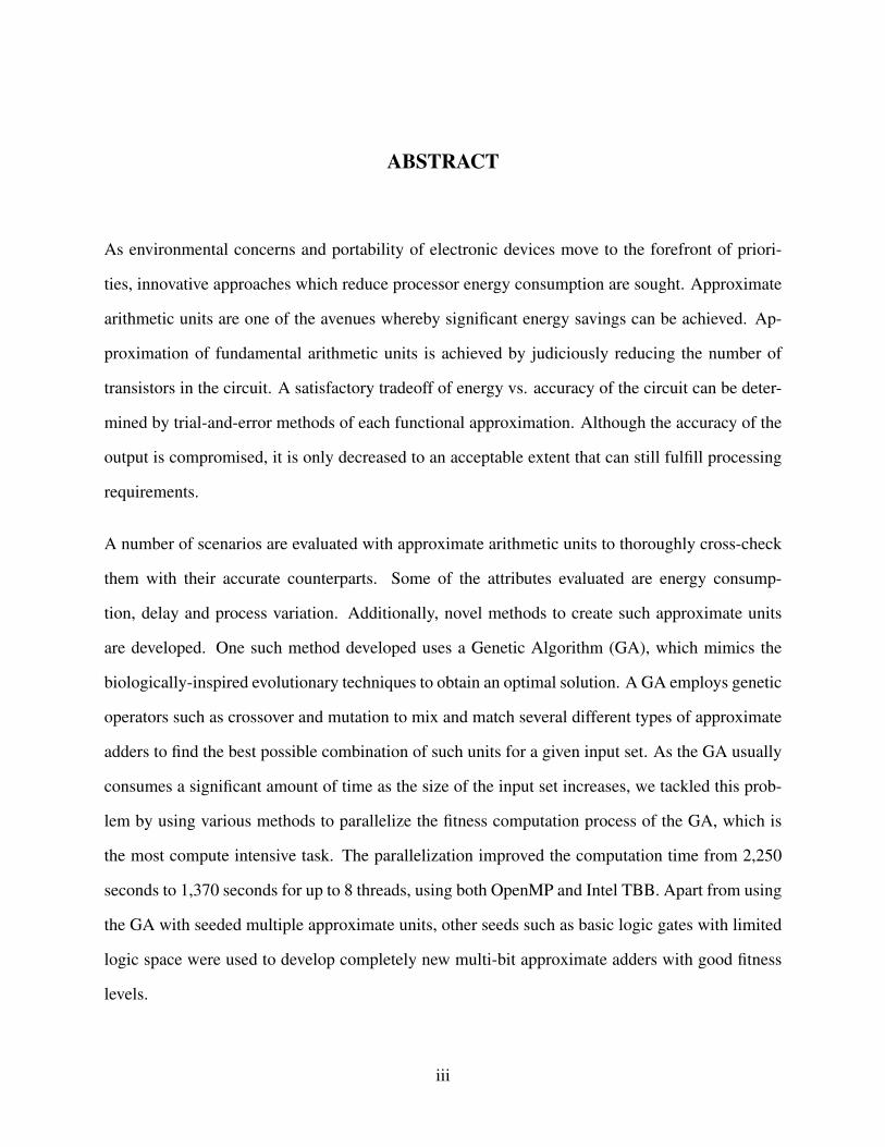
ABSTRACT
As environmental concerns and portability of electronic devices move to the forefront of priori-
ties, innovative approaches which reduce processor energy consumption are sought. Approximate
arithmetic units are one of the avenues whereby significant energy savings can be achieved. Ap-
proximation of fundamental arithmetic units is achieved by judiciously reducing the number of
transistors in the circuit. A satisfactory tradeoff of energy vs. accuracy of the circuit can be deter-
mined by trial-and-error methods of each functional approximation. Although the accuracy of the
output is compromised, it is only decreased to an acceptable extent that can still fulfill processing
requirements.
A number of scenarios are evaluated with approximate arithmetic units to thoroughly cross-check
them with their accurate counterparts. Some of the attributes evaluated are energy consump-
tion, delay and process variation. Additionally, novel methods to create such approximate units
are developed. One such method developed uses a Genetic Algorithm (GA), which mimics the
biologically-inspired evolutionary techniques to obtain an optimal solution. A GA employs genetic
operators such as crossover and mutation to mix and match several different types of approximate
adders to find the best possible combination of such units for a given input set. As the GA usually
consumes a significant amount of time as the size of the input set increases, we tackled this prob-
lem by using various methods to parallelize the fitness computation process of the GA, which is
the most compute intensive task. The parallelization improved the computation time from 2,250
seconds to 1,370 seconds for up to 8 threads, using both OpenMP and Intel TBB. Apart from using
the GA with seeded multiple approximate units, other seeds such as basic logic gates with limited
logic space were used to develop completely new multi-bit approximate adders with good fitness
levels.
iii

The effect of process variation was also calculated. As the number of transistors is reduced, the
distribution of the transistor widths and gate oxide may shift away from a Gaussian Curve. This re-
sult was demonstrated in different types of single-bit adders with the delay sigma increasing from
6psec to 12psec, and when the voltage is scaled to Near-Threshold-Voltage (NTV) levels sigma
increases by up to 5psec. Approximate Arithmetic Units were not affected greatly by the change
in distribution of the thickness of the gate oxide. Even when considering the 3-sigma value, the
delay of an approximate adder remains below that of a precise adder with additional transistors.
Additionally, it is demonstrated that the GA obtains innovative solutions to the appropriate com-
bination of approximate arithmetic units, to achieve a good balance between energy savings and
accuracy.
iv

Dedicated to my father, who was the rock behind my back
v

ACKNOWLEDGMENTS
The author wishes to express his gratitude to Dr. Ronald DeMara, advisor and committee chairman,
for his technical guidance and unlimited support.
The author would like to thank the thesis committee members for all of their guidance through this
process.
Appreciation is also extended to Rizwan Ashraf for his technical assistance.
vi
TABLE OF CONTENTS
LIST OF FIGURES . . . . . . . . . . . . . . . . . . . . . . . . . . . . . . . . . . . . . . ix
LIST OF TABLES . . . . . . . . . . . . . . . . . . . . . . . . . . . . . . . . . . . . . . . xi
CHAPTER 1: INTRODUCTION . . . . . . . . . . . . . . . . . . . . . . . . . . . . . . . 1
Significance of the Problem . . . . . . . . . . . . . . . . . . . . . . . . . . . . . . . . . 2
Types of Approximations . . . . . . . . . . . . . . . . . . . . . . . . . . . . . . . . . . 3
Voltage Over-scaling . . . . . . . . . . . . . . . . . . . . . . . . . . . . . . . . . 4
Probabilistic Computing . . . . . . . . . . . . . . . . . . . . . . . . . . . . . . . 5
Functional Approximation . . . . . . . . . . . . . . . . . . . . . . . . . . . . . . 5
Evolutionary Algorithms . . . . . . . . . . . . . . . . . . . . . . . . . . . . . . . . . . 6
Genetic Algorithms . . . . . . . . . . . . . . . . . . . . . . . . . . . . . . . . . . 7
Fundamentals of Genetic Algorithms . . . . . . . . . . . . . . . . . . . . 7
Parallelism in GAs . . . . . . . . . . . . . . . . . . . . . . . . . . . . . . 8
Challenges facing Evolution of Approximate Adders . . . . . . . . . . . . . . . . . . . 13
Contribution of Thesis . . . . . . . . . . . . . . . . . . . . . . . . . . . . . . . . . . . 15
Organization of Thesis . . . . . . . . . . . . . . . . . . . . . . . . . . . . . . . . . . . 15
vii

CHAPTER 2: RELATED WORK . . . . . . . . . . . . . . . . . . . . . . . . . . . . . . 17
Types of Functional Approximation . . . . . . . . . . . . . . . . . . . . . . . . . . . . 17
Conventional Mirror Adder . . . . . . . . . . . . . . . . . . . . . . . . . . . . . . 21
Approximation 1 . . . . . . . . . . . . . . . . . . . . . . . . . . . . . . . . . . . 21
Approximation 2 . . . . . . . . . . . . . . . . . . . . . . . . . . . . . . . . . . . 22
Approximation 3 . . . . . . . . . . . . . . . . . . . . . . . . . . . . . . . . . . . 23
Energy Evaluation . . . . . . . . . . . . . . . . . . . . . . . . . . . . . . . . . . . . . . 23
CHAPTER 3: METHODOLOGY . . . . . . . . . . . . . . . . . . . . . . . . . . . . . . 27
Experimental Results . . . . . . . . . . . . . . . . . . . . . . . . . . . . . . . . . . . . 28
Parallel Genetic Algorithm . . . . . . . . . . . . . . . . . . . . . . . . . . . . . . 32
CHAPTER 4: EXPERIMENTAL RESULTS . . . . . . . . . . . . . . . . . . . . . . . . . 37
RCA Adders . . . . . . . . . . . . . . . . . . . . . . . . . . . . . . . . . . . . . . . . . 38
CLA Adder . . . . . . . . . . . . . . . . . . . . . . . . . . . . . . . . . . . . . . . . . 46
CHAPTER 5: CONCLUSION . . . . . . . . . . . . . . . . . . . . . . . . . . . . . . . . 49
APPENDIX : SIMULATION CODE . . . . . . . . . . . . . . . . . . . . . . . . . . . . 53
LIST OF REFERENCES . . . . . . . . . . . . . . . . . . . . . . . . . . . . . . . . . . . 68
viii
LIST OF FIGURES
Figure 1.1: Evolutionary Algorithms . . . . . . . . . . . . . . . . . . . . . . . . . . . . 6
Figure 1.2: Solution Space [1] . . . . . . . . . . . . . . . . . . . . . . . . . . . . . . . . 7
Figure 1.3: Normalized error distance versus the number of lower bits [2] . . . . . . . . . 12
Figure 1.4: Relation between error metrics . . . . . . . . . . . . . . . . . . . . . . . . . 13
Figure 1.5: Normalized error distance [2] . . . . . . . . . . . . . . . . . . . . . . . . . . 14
Figure 1.6: Organization of Thesis . . . . . . . . . . . . . . . . . . . . . . . . . . . . . 16
Figure 2.1: Quality Constraint Circuit [3] . . . . . . . . . . . . . . . . . . . . . . . . . . 18
Figure 2.2: Quality Constraint Circuit [4] . . . . . . . . . . . . . . . . . . . . . . . . . . 19
Figure 2.3: Recursive multiplier used in [5] . . . . . . . . . . . . . . . . . . . . . . . . . 20
Figure 2.4: Pipelined adder implementation of accurate adder and approximate adder
used in [6] . . . . . . . . . . . . . . . . . . . . . . . . . . . . . . . . . . . . 20
Figure 2.5: Error Detection and Correction Mechanism used in [6] . . . . . . . . . . . . 21
Figure 2.6: Conventional Mirror Adder [7] . . . . . . . . . . . . . . . . . . . . . . . . . 22
Figure 2.7: Approximate Mirror Adder 1 [8] . . . . . . . . . . . . . . . . . . . . . . . . 22
Figure 2.8: Approximate Mirror Adder 3 [8] . . . . . . . . . . . . . . . . . . . . . . . . 23
Figure 2.9: Approximate Mirror Adder 4 [8] . . . . . . . . . . . . . . . . . . . . . . . . 24
ix
Figure 3.1: Gaussian uniform distribution . . . . . . . . . . . . . . . . . . . . . . . . . . 28
Figure 3.2: Flow of the GA . . . . . . . . . . . . . . . . . . . . . . . . . . . . . . . . . 30
Figure 3.3: Crossover Operation . . . . . . . . . . . . . . . . . . . . . . . . . . . . . . 31
Figure 3.4: Carry Dependencies in RCA . . . . . . . . . . . . . . . . . . . . . . . . . . 32
Figure 4.1: Performance without OpenMP . . . . . . . . . . . . . . . . . . . . . . . . . 39
Figure 4.2: Performance with OpenMP included . . . . . . . . . . . . . . . . . . . . . . 39
Figure 4.3: Fitness Evolved when on a subset of inputs restricted to maximum fitness
value of 220 . . . . . . . . . . . . . . . . . . . . . . . . . . . . . . . . . . . 43
Figure 4.4: Fitness Evolved when the number of gates was restricted to 16 for a 4 bit adder 44
Figure 4.5: Fitness Evolved when Approximate Adders are used to implement a 4-bit
Adder . . . . . . . . . . . . . . . . . . . . . . . . . . . . . . . . . . . . . . 45
Figure 4.6: Approximate CLA Adder . . . . . . . . . . . . . . . . . . . . . . . . . . . . 46
Figure 4.7: Accurate CLA Adder . . . . . . . . . . . . . . . . . . . . . . . . . . . . . . 47
x
LIST OF TABLES
Table 2.1: Truth Table for Conventional Full Adder and Approximations 1, 2 and 3 [7] . 24
Table 4.1: Results of Accurate Mirror Adder . . . . . . . . . . . . . . . . . . . . . . . 38
Table 4.2: Results of Approximate Mirror Adder I . . . . . . . . . . . . . . . . . . . . 38
Table 4.3: Results of Approximate Mirror Adder II . . . . . . . . . . . . . . . . . . . . 40
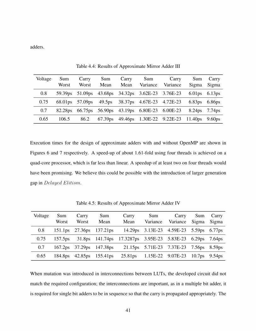
Table 4.4: Results of Approximate Mirror Adder III . . . . . . . . . . . . . . . . . . . . 41
Table 4.5: Results of Approximate Mirror Adder IV . . . . . . . . . . . . . . . . . . . 41
Table 4.6: Propagation Delay and Power Consumption for Approximate Adders . . . . . 42
Table 4.7: Truth Table for Conventional CLA and Approximate CLA . . . . . . . . . . 45
Table 4.8: Results of Approximate CLA . . . . . . . . . . . . . . . . . . . . . . . . . . 47
Table 5.1: Summary of Approximate Adder Performance . . . . . . . . . . . . . . . . 50
xi
CHAPTER 1: INTRODUCTION
As environmental concerns and portability of electronic devices move to the forefront of priorities,
it is important for us to find ways to reduce the power consumption of our devices. A number of
ways have been proposed to reduce the power consumption of devices. The need for higher energy
efficiency in recent times has pushed the industry and academia to find various other avenues
to decrease power consumption. Some of the common methods of reducing energy consumptions
include voltage scaling, Probabilistic CMOS (PCMOS), algorithmic truncation and approximation.
These methods are reviewed briefly here. Various mechanisms are used to reduce errors due to
voltage overscaling, one of the mechanisms of particular interest is shown in [9] . In [9] slack
redistribution is used to gracefully degrade the circuit. Use of PCMOS is another way of reducing
the energy cost without compromising on accuracy by a large margin as shown in [10]. [10] states
that all MOS devices are inherently probabilistic rather than deterministic, it takes advantage of
this probability in cases where noise is present to yield accurate results. [10] Implements PCMOS
in System on Chips (SoC) to form a Probabilistic System on Chip (PSoC). The third method i.e.
algorithmic truncation is a software level based solution, this solution is usually compared with
hardware level approximation as shown in [7]. Algorithmic truncation usually refers to methods
of removing a fixed number of LSBs from the output or input. Another method of algorithmic
adaptation would be to skip certain steps in the algorithm in return for reduced accuracy and power
savings. Hardware approximation refers to reduction in the size of critical path by reducing the
number of transistors in the path.
The paper [15] illustrated the various ways a Genetic Algorithm can be parallelized, this paper
delves into four levels of parallelism i.e. Parallelism of fitness evaluation, Parallelism of repro-
duction (selection, crossover etc.), Parallelism of groups (Population is sub-divided into groups
and then they are evolved separately, with a chance of interaction after each generation), the paper
1

also defines the various levels of details a parallel genetic algorithm can be implemented The sec-
ond paper uses a Cartesian Genetic Algorithm to develop various adders at design-time, also the
adders developed undergo testing under various error metrics, they also incorporate redundancy in
their method where not all the gates are used for obtaining an output, a downside to this could be
the area size, the paper does not describe how the other gates are excluded and how they can be
included i.e. the method used. It uses two levels of fitness calculation to test the error range of
the circuit. The third paper apart from developing their own parallel multiplier, they also compare
various types of multipliers and where they could be used, they give design guidelines to use when
implementing it in EDA tools.
Adnan
Significance of the Problem
For most purposes nature seems to approximate in many situations, for example the flow of a fluid,
there are always a number of extraneous factors responsible for the flow of the fluid, unless the
fluid is under ideal conditions, only then is it possible for science to truly predict the flow of a
fluid. Signal Processing is similar to such a problem, analogous to a fluid, it is inherently tolerant
to approximations and error. We try to exploit this inherent tolerance to errors to reduce Power
consumption and area used by computation. Such kind of inherent tolerance can also be seen in
Machine Learning, and Data Mining, which show significant algorithmic resilience [3]. This trait
can be attributed to redundancies in input data-sets, lack of a definitive result or the ability of an
algorithm to average out the errors. In general, most of the signal processing applications require
high-end processing powers to compute precisely and expend large amounts of power to compute
precisely. Approximation could save a lot of power in applications where 100% accuracy is not
2

a necessity. As it removes the unnecessary slack of more than required accuracy using various
methods such as voltage over-scaling, functional approximation etc.
We functionally approximate many arithmetic circuits to improve delay and power consumption in
adders. We also observe the effects of process variation as illustrated in the tables further into the
text. In combination with Genetic Algorithms(GA) we develop combinations of multi-bit adders
with a threshold accuracy and major savings in power. The GAs help us find the right combina-
tion of accuracy and power savings, where the trade-off is just right such that the accuracy is not
degraded too much and the power savings are maximum. Process variation also seems to play
a significant role in smaller bit-width adders, but as the size of the arithmetic unit increases, the
distribution evens out and the sigma value seems to remain within normal ranges in approximate
units.
Types of Approximations
Approximations can be broadly classified as over-scaling based approximation methods which
introduce errors due to timing constraints, some examples of over-scaling based approximations
include Voltage Approximation. Usually in over-scaling based approximations the slack time is
progressively decreased until there’s not enough time for the circuit to latch on to the value, which
causes the circuit to use the last value latched as the current value, in voltage approximation, the
VDD or VTH is progressively reduced until such temporal errors occur. For the sake of simplic-
ity we include Probabilistic Computing in this category and functional approximation methods,
which reduce the number of transistors in arithmetic units to introduce errors, maximum power
savings are usually obtained by functional approximations. This is due to the fact that the parasitic
capacitances, and dynamic, and static power consumption are drastically reduced as the number of
transistors reduces, as shown in the results. A beneficial side-effect of reduced transistors is that
3
the delay also decreases significantly, process variation does not seem to affect the delay enough
to increase the delay and power consumption to equal that of an accurate unit. Another type of
approximation is known as algorithmic truncation, in this method a part of the code or number is
truncated, in case of code truncation, a for loop could be truncated by reducing the number of times
it needs to run, for example if a for loop needs to loop 1000 times to obtain an accurate result, it
could instead run for 200 loops and get a nearly accurate result in case of binary truncation a part
of the binary number is removed usually a set number of LSBs and replaced by 0’s, for example if
a binary number 111111112 is to be computed on instead of the hardware receiving 111111112 it
receives 111100002 and the hardware performs the arithmetic operation on the first four most sig-
nificant bits. The three examples of voltage over-scaling, Probabilistic Computing and functional
approximation are explained further in the following sections.
Voltage Over-scaling
Orthodox designs take into account various redundancies to select a high VDD to accommodate any
errors occurring due to process variation, timing errors, aging etc. However, when VDD is scaled
below the critical voltage, the number of errors drastically increase and hence in turn drastically
degrade the output quality One way to improve signal quality in such cases is to introduce error
correcting mechanisms. [11] introduces an approach under algorithmic noise tolerance. This type
of circuit contains two blocks namely the main computing circuit and an error correcting circuit.
The main computing circuit is run on a low VDD whereas the simpler error correcting circuit runs
on a higher voltage. As the error correcting circuit consists of lesser number of transistors than
the main computing circuit due to which the energy savings are notable. In certain cases Error
Correcting Codes (ECC) are used to compensate for the errors caused by over-scaling.
4
Probabilistic Computing
As CMOS technology scales down to the 10nm region, hurdles due to noise pose several challenges
as explained in [10]. Probability based CMOS technology looks upon noise as a resource which
can be harnessed [12]. Probabilistic CMOS have been known to yield better Energy Performance
Product (EPP). EPP is defined as the product of energy consumed and running time. In [10]
PCMOS is defined as the CMOS which is affected by thermal (ambient) noise. The computation
in such circuits use probabilistic algorithms to reduce the effect of noise in the output. In addition
to the above qualities, PCMOS can also generate high quality random bits. These random bits
are important, as they are used extensively in probabilistic algorithms. The circuits implementing
PCMOS typically contain a deterministic host processor, which is used to compute most of the
control intensive components of an application and a probabilistic co-processor, which is used as
an accelerator.
Functional Approximation
The process of removing transistors from a circuit to obtain a less than accurate circuit can be
defined as Functional Approximation. The transistors removed are usually from the critical path to
reduce the delay along with power consumption, but if the critical path is untouchable especially
in cases where the MSB could be of significant importance, the transistors are removed from other
areas which affect LSBs more often than MSBs, functional approximation gives us the most sav-
ings, as it reduces the cascading effect most times, removes a number of unnecessary capacitances
present in the accurate circuits. In this thesis we concentrate on adders, we functionally approxi-
mate a number of adders including the CLA Adder and Ripple Carry Adder and determine their
delay under various conditions and process variation is also taken into account in these conditions.
5
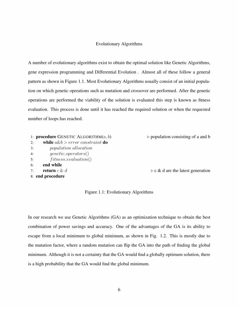
Evolutionary Algorithms
A number of evolutionary algorithms exist to obtain the optimal solution like Genetic Algorithms,
gene expression programming and Differential Evolution . Almost all of these follow a general
pattern as shown in Figure 1.1. Most Evolutionary Algorithms usually consist of an initial popula-
tion on which genetic operations such as mutation and crossover are performed. After the genetic
operations are performed the viability of the solution is evaluated this step is known as fitness
evaluation. This process is done until it has reached the required solution or when the requested
number of loops has reached.
1: procedure GENETIC ALGORITHM(a, b) . population consisting of a and b2: while a&b > error constraint do3: population allocation4: genetic operators()5: fitness evaluation()6: end while7: return c & d . c & d are the latest generation8: end procedure
Figure 1.1: Evolutionary Algorithms
In our research we use Genetic Algorithms (GA) as an optimization technique to obtain the best
combination of power savings and accuracy. One of the advantages of the GA is its ability to
escape from a local minimum to global minimum, as shown in Fig. 1.2. This is mostly due to
the mutation factor, where a random mutation can flip the GA into the path of finding the global
minimum. Although it is not a certainty that the GA would find a globally optimum solution, there
is a high probability that the GA would find the global minimum.
6
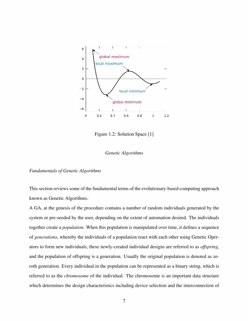
Figure 1.2: Solution Space [1]
Genetic Algorithms
Fundamentals of Genetic Algorithms
This section reviews some of the fundamental terms of the evolutionary-based computing approach
known as Genetic Algorithms.
A GA, at the genesis of the procedure contains a number of random individuals generated by the
system or pre-seeded by the user, depending on the extent of automation desired. The individuals
together create a population. When this population is manipulated over time, it defines a sequence
of generations, whereby the individuals of a population react with each other using Genetic Oper-
ators to form new individuals, these newly-created individual designs are referred to as offspring,
and the population of offspring is a generation. Usually the original population is denoted as ze-
roth generation. Every individual in the population can be represented as a binary string, which is
referred to as the chromosome of the individual. The chromosome is an important data structure
which determines the design characteristics including device selection and the interconnection of
7
the individual circuit being represented. The performance of an individual can be evaluated by us-
ing a fitness function. Fitness can be specified as a cost function including mean error and resource
usage according to a user-defined value called the error criterion.
As the GA runs, it performs Genetic Operators such as a crossover, which is a method by which
interacting individuals exchange binary data, replacing the original data, to exchange subcircuits
from high-performing parents to offspring. To make sure that the GA does not converge to a local
solution, a mutation function is introduced, which randomly changes a value in the chromosome.
The probability of mutation is kept to low levels in the range of one random modification for every
1000000 bits. The mutation operator is kept to such low levels to prevent the GA from perform-
ing a random search. In certain GAs, the fittest individual of each generation is always retained
through successive generations without any modification, this process of selection is referred to as
elitism. In cases where elitism is not used, individuals are selected based on probability, which is
a function of its fitness. If the fitness level of an individual is high, then it has a higher chance of
being selected and vice-versa.
Parallelism in GAs
The power of GAs is given by schema theorem [13], the schema theorem is a set of symbols
used in a string {1*00*1} where * can either be one or zero. The order of the schema o(H) is
defined as the number of fixed positions in the schema, while δ(H) is the distance between the
first and the last specific positions. The order of the string 1*00*1 is four and the defining length
is five. The schema theorem states that the fitness of a short schemata with higher fitness than the
average population will increase exponentially in successive generations [14]. It is expressed by
the equation:
E(m(H, t+ 1)) ≥ m(H, t)f(H)
at[1− p] (1.1)
8
where, m(H, t) is the number of strings belonging to schema H , f(H) is the average fitness of
schema H , at is the average fitness at generation t and p is the probability that a mutation could
destroy a schema. Here p is defined from the following equation:
p =δ(H)
l − 1pc + o(H)pm (1.2)
where, o(H) is the order of the schema, l is the length of the code, pm is the probability of mutation
and pc is the probability of crossover [14]. From equation (1) and (2) it can be inferred that it is
advantageous to keep the chromosomes as short as possible. Also, from the schema theorem it
can be inferred that even in a sequential algorithm, it is possible for the algorithm to handle o(N3)
schema at a time for a population of N individuals. Thus the GAs can handle large number of
schema at a time, which can be considered as inherent parallelism [13].
Most GAs can be subdivided into four parts based on amount of computation namely:
• Population Selection
• Crossover and Mutation
• Fitness Evaluation
• Offspring Generation
The list also illustrates where a GA could be parallelized with greater efficiency overall. Apart
from this a GA can also be parallelized based on its detailed algorithmic flow [13]. Some of the
methods mentioned in [13] are
• Parallelism of Individual’s Fitness: The fitness evaluation of a population consumes the most
amount of power and time, depending on the algorithm and fitness dependencies, the fitness
calculation can be parallelized.
9
• Parallelism of Occurrence of Offspring: Processes by which offspring are produced could
be parallelized, for example, when a crossover takes place only two parents are used in a
single crossover, while the rest of the population lies idle, this can be rectified in parallel
computation by performing crossover simultaneously over the entire population.
• Parallelism Based on Population Grouping: In certain cases, the population of individuals
could be subdivided into smaller sub-groups which could be assigned to different threads.
A number of methods have been proposed to quantify the errors occurring in approximate circuits,
some methods are similar to Hamming Distance. In this thesis we review three types of error
measurement techniques as mentioned in [2].
Error Distance
The measurement technique developed [2] measures the precision of approximate circuits.
This method is termed as Error Distance. Error Distance is the arithmetic distance between
two binary values i.e. the arithmetic distance between the predicted/required value and the
obtained/output value. For example, let us consider a Full Adder, if the exact output of the
Sum is 100101, but the circuit gives an output of 100100, then the error distance between the
two values is said to be one, similar to Hamming distance. But if the output was 101111”
then the error distance would be ten. It can be seen that the value of error distance (ED)
increases or decreases depending on the position of the incorrect bit. [2] defines ED with
equation(1.3)
ED(a, b) = |a− b| = |Σja[i] ∗ 2i − Σib[j] ∗ 2j| (1.3)
For a non-deterministic application, the output is probabilistic and usually follows a set
distribution for a given input ai. In this case ED is defined as the weighted average of all
10
possible outputs to the nominal output. Assume that for a given input, the output has a
nominal value b, but it can take any value given in a set of vectors bj (1<j<r) [2]. The ED
of the output, in such cases, is given by equation (1.4) as shown in [2]
di = ΣjED(bj, b) ∗ pj (1.4)
where, pj is the output probability of bj (1<j<r)
Mean Error Distance
Mean Error Distance is used in cases where the inputs are probabilistic and thus each input
occurs only at a particular probability. The mean error distance (MED) of a circuit is defined
as the mean value of the EDs of all possible outputs for each input [2] . Assume that the
input is a set of vectors ai and that each vector occurs with a probability of qi [2]. Then, the
MED, dm of the circuit is given by
dm = Σdi ∗ qi (1.5)
Where, di is the ED of outputs for input ai which can be computed by (1.5).
As an example assume a NOT gate, the probability of the input to the NOT gate being 1 is
0.7 and if the output of the NOT gate is 1 even if the input is 1. In this case the MED is given
by ED multiplied by the probability (0.7) which is equal to 0.7 as the ED is 1 in this case.
In case of multiple outputs, the ED is individually calculated and then multiplied with indi-
vidual probabilities and after the values are calculated, all the values are summed with each
other to obtain the final value.
11
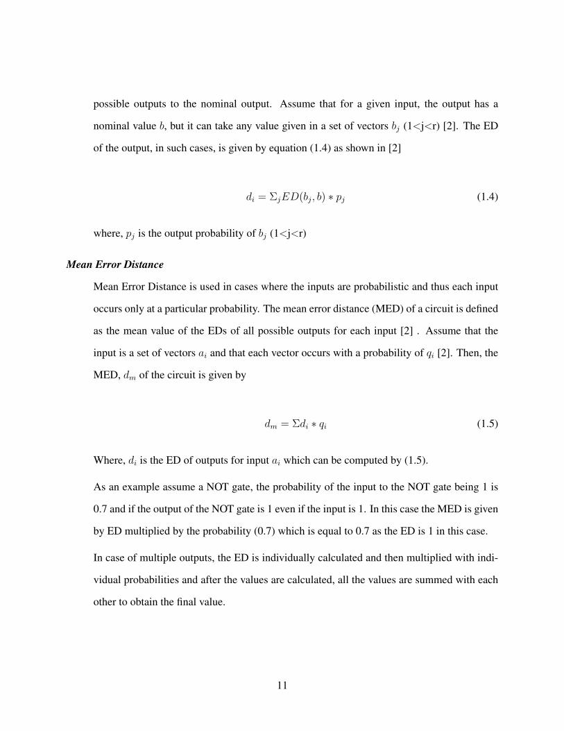
Figure 1.3: Normalized error distance versus the number of lower bits [2]
Normalized Error Distance
MED increases with increase in the number of lower bits. It is therefore biased to use MED
to compare between two adders with different lower bits as the maximum value of error that
can be effectively reached has also changed [2]. To overcome this limitation Normalized
Error Distance (NED) is used. NED is defined as
dn = dm/D (1.6)
Where, dm is the MED and D is the maximum value of the error. The maximum value
is usually 2n for n lower bits [2]. We use the fitness function used in [15]. It requires
multiplication of the number of combinations possible in a truth table multiplied by the
number of outputs to get the maximum fitness value. Hence, we can denote the formula as
given in equation (1.6).
12

ErrorDistance
Multiply by Qi
Mean ErrorDistance
Divide by D
NormalizedError
Distance
Figure 1.4: Relation between error metrics
Challenges facing Evolution of Approximate Adders
Currently the important facet of a GA is the fitness evaluation, it is also the most computation
intensive task of the GA. One of the problems we have tried to tackle here is the evaluation
time of complex solutions. In this case it was a multi-bit adder where the input space is
enormous, in such cases we have used parallelism to generate the results faster by using
multiple threads and efficient programming.
13

Figure 1.5: Normalized error distance [2]
Another problem is to generate sequential circuits using parallel methods due to which the inter-
connections are performed incorrectly. Additionally in some cases the GA would not converge to
a globally optimum solution, in such cases the mutation factor needs to be set by trial and error
method until a proper solution is obtained, this is an extremely time consuming process. Also
GA can be further optimized by combining them with other optimization algorithms, where the
coefficients can be altered by the GA or vice versa. Also some GAs face problems with random
seeds, where the seeds aren’t random enough for complex algorithms to take a different path at
every run. Fortunately the population size is relatively low in our algorithm, hence the effect of
pseudo-randomness is not pronounced. Some other challenges in implementing a GA is to iden-
tify portions of GA and areas where it could be potentially parallelized with gains, parallelizing
at every opportunity does not yield good results, as in some cases the overhead of multi-threading
is greater than the gains obtained from parallelizing a particular area. As such all the loops hence
14
were not parallelized as it was more efficient to run them on a single thread rather than multi-
ple thread. Another issue faced was the placing of certain volatile variables in the cache, which
were being constantly modified during runtime, these variables had to me manually identified and
marked volatile to prevent invalidation of the cache line.
Contribution of Thesis
The contributions of this Thesis are:
• Effect of Process Variation on Approximate Adders at NTV: Determines the range of values
possible for delays and power consumption under the effect of process variation and analyzes
how it affects a larger system of approximate units,
• Evolution of approximate systems using GAs: Identifies various dependencies in Adder cir-
cuits and how it affects the performance of the GA and explores the various avenues through
which the GA could be parallelized to obtain higher efficiency and lower process time, and
• Development of Approximate Adders: Develops a new approximate adder from a CLA Adder
with better performance and lower delays for the sum output.
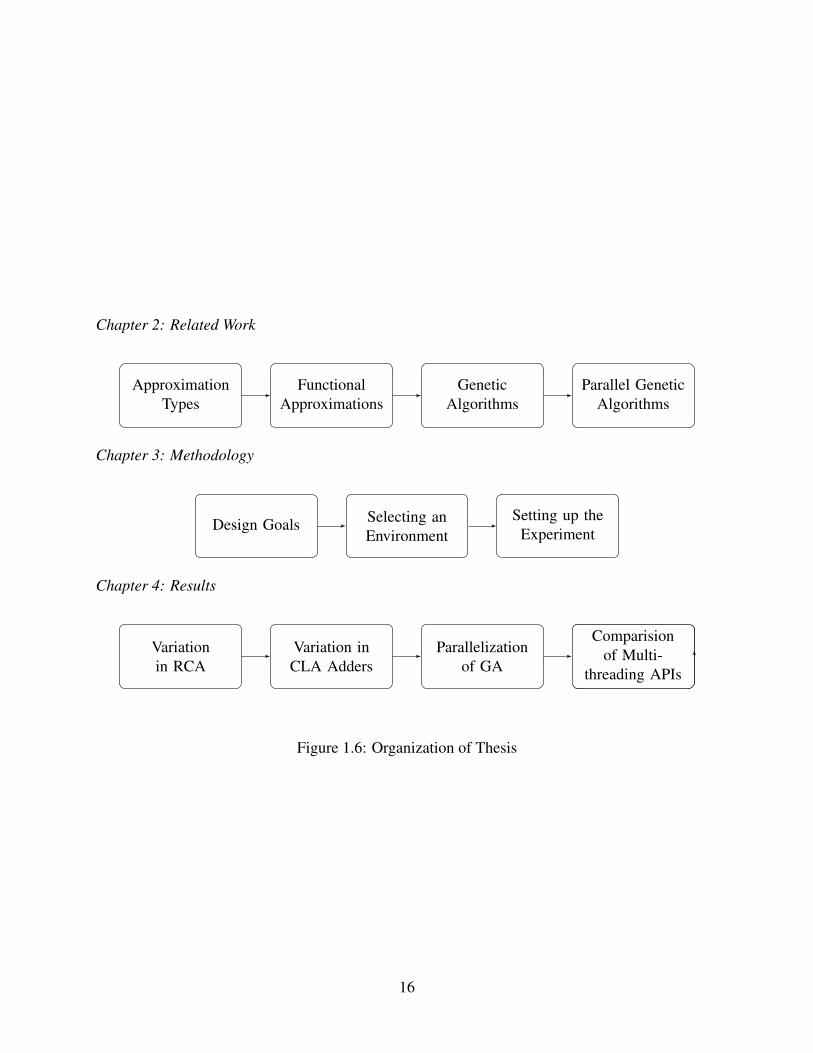
Organization of Thesis
The organization of thesis is depicted in Figure 1.6. First, related work is reviewed in Chapter 2.
Chapter 3 defines the research and experimental methodology which was employed, including GA
configuration for the approximate adder circuits being evaluated. Chapter 4 presents results for
variation in RCAs and CLAs. It also discusses lessons learned for using parallel GAs to optimize
these circuits.
15
Chapter 2: Related Work
ApproximationTypes
FunctionalApproximations
GeneticAlgorithms
Parallel GeneticAlgorithms
Chapter 3: Methodology
Design Goals Selecting anEnvironment
Setting up theExperiment
Chapter 4: Results
Variationin RCA
Variation inCLA Adders
Parallelizationof GA
Adder Devel-oped using GA
Comparisionof Multi-
threading APIs
Figure 1.6: Organization of Thesis
16
CHAPTER 2: RELATED WORK
Approximate computing offers a promising approach for reduced energy operation for applications
which can tolerate some imprecision. There are many types of approximate circuits, including
those constructed by voltage over-scaling and over-clocking [16] and others as mentioned in [17–
20]. However, this thesis uses approximate adders which utilize lesser number of transistors than
the original accurate design. The Adders used in this thesis are obtained from [7]. As these adders
are analyzed in a manner which is suited to the application presented in our research. In this
section we discuss and analyze the three different types of adders used and the accurate adder. The
accurate adder is the reference adder from which the other adders are derived.
Types of Functional Approximation
A number of methods to approximate circuits have been proposed including the trial and error
method. Most of the approximations have been done manually, carefully reducing the number of
transistors in a circuit using the trial and error method. Most of the efforts concentrate on reducing
the length of the critical path. Some other methods such as SALSA [3] and MACACO [4] use
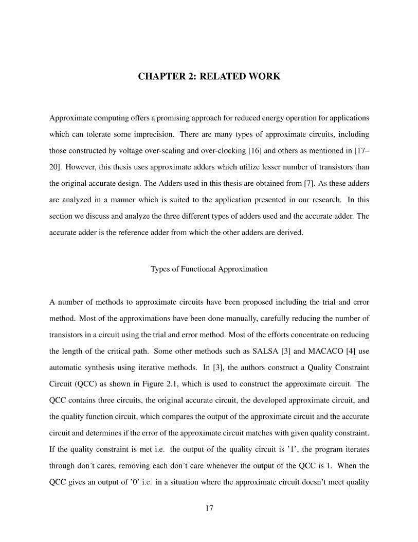
automatic synthesis using iterative methods. In [3], the authors construct a Quality Constraint
Circuit (QCC) as shown in Figure 2.1, which is used to construct the approximate circuit. The
QCC contains three circuits, the original accurate circuit, the developed approximate circuit, and
the quality function circuit, which compares the output of the approximate circuit and the accurate
circuit and determines if the error of the approximate circuit matches with given quality constraint.
If the quality constraint is met i.e. the output of the quality circuit is ’1’, the program iterates
through don’t cares, removing each don’t care whenever the output of the QCC is 1. When the
QCC gives an output of ’0’ i.e. in a situation where the approximate circuit doesn’t meet quality
17
constraints, the platform reverses to its last valid state and this last output is considered as the valid
situation.
Figure 2.1: Quality Constraint Circuit [3]
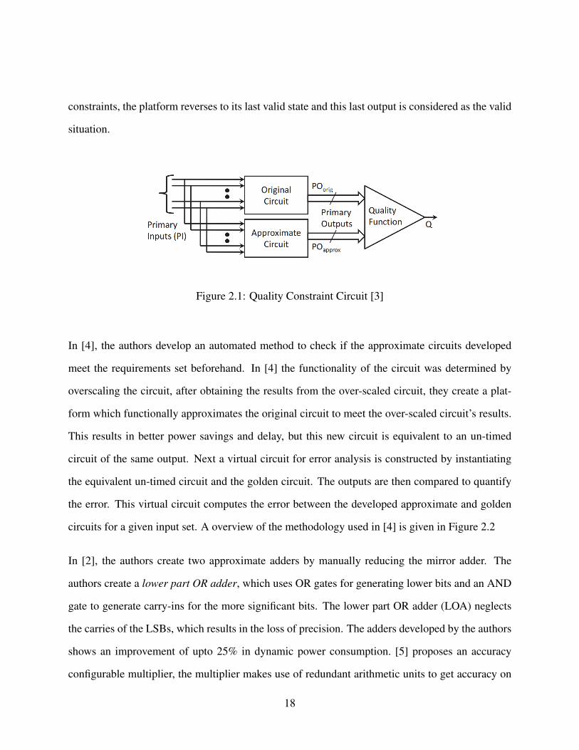
In [4], the authors develop an automated method to check if the approximate circuits developed
meet the requirements set beforehand. In [4] the functionality of the circuit was determined by
overscaling the circuit, after obtaining the results from the over-scaled circuit, they create a plat-
form which functionally approximates the original circuit to meet the over-scaled circuit’s results.
This results in better power savings and delay, but this new circuit is equivalent to an un-timed
circuit of the same output. Next a virtual circuit for error analysis is constructed by instantiating
the equivalent un-timed circuit and the golden circuit. The outputs are then compared to quantify
the error. This virtual circuit computes the error between the developed approximate and golden
circuits for a given input set. A overview of the methodology used in [4] is given in Figure 2.2
In [2], the authors create two approximate adders by manually reducing the mirror adder. The
authors create a lower part OR adder, which uses OR gates for generating lower bits and an AND
gate to generate carry-ins for the more significant bits. The lower part OR adder (LOA) neglects
the carries of the LSBs, which results in the loss of precision. The adders developed by the authors
shows an improvement of upto 25% in dynamic power consumption. [5] proposes an accuracy
configurable multiplier, the multiplier makes use of redundant arithmetic units to get accuracy on
18
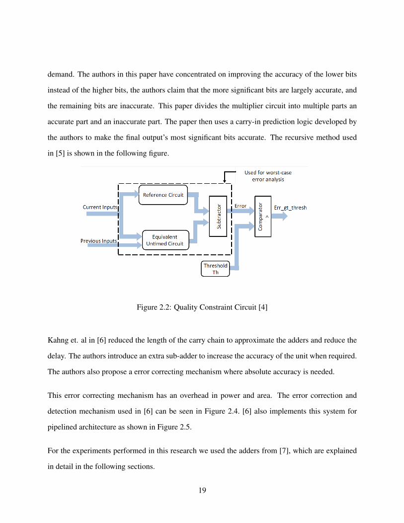
demand. The authors in this paper have concentrated on improving the accuracy of the lower bits
instead of the higher bits, the authors claim that the more significant bits are largely accurate, and
the remaining bits are inaccurate. This paper divides the multiplier circuit into multiple parts an
accurate part and an inaccurate part. The paper then uses a carry-in prediction logic developed by
the authors to make the final output’s most significant bits accurate. The recursive method used
in [5] is shown in the following figure.
Figure 2.2: Quality Constraint Circuit [4]
Kahng et. al in [6] reduced the length of the carry chain to approximate the adders and reduce the
delay. The authors introduce an extra sub-adder to increase the accuracy of the unit when required.
The authors also propose a error correcting mechanism where absolute accuracy is needed.
This error correcting mechanism has an overhead in power and area. The error correction and
detection mechanism used in [6] can be seen in Figure 2.4. [6] also implements this system for
pipelined architecture as shown in Figure 2.5.
For the experiments performed in this research we used the adders from [7], which are explained
in detail in the following sections.
19
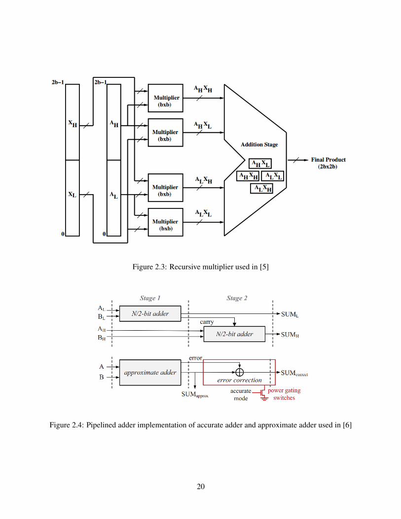
Figure 2.3: Recursive multiplier used in [5]
Figure 2.4: Pipelined adder implementation of accurate adder and approximate adder used in [6]
20
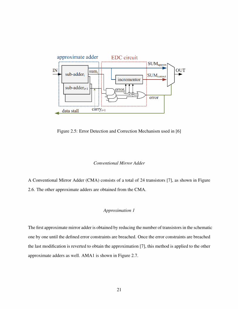
Figure 2.5: Error Detection and Correction Mechanism used in [6]
Conventional Mirror Adder
A Conventional Mirror Adder (CMA) consists of a total of 24 transistors [7], as shown in Figure
2.6. The other approximate adders are obtained from the CMA.
Approximation 1
The first approximate mirror adder is obtained by reducing the number of transistors in the schematic
one by one until the defined error constraints are breached. Once the error constraints are breached
the last modification is reverted to obtain the approximation [7], this method is applied to the other
approximate adders as well. AMA1 is shown in Figure 2.7.
21
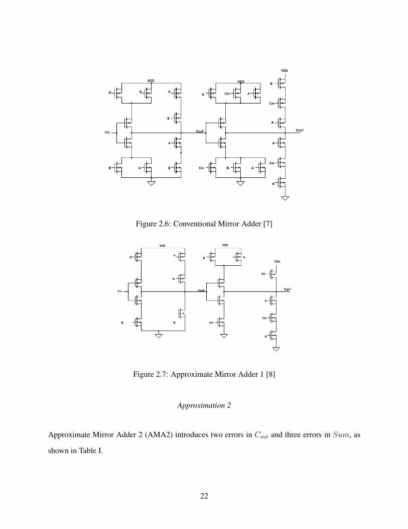
Figure 2.6: Conventional Mirror Adder [7]
Figure 2.7: Approximate Mirror Adder 1 [8]
Approximation 2
Approximate Mirror Adder 2 (AMA2) introduces two errors in Cout and three errors in Sum, as
shown in Table I.
22
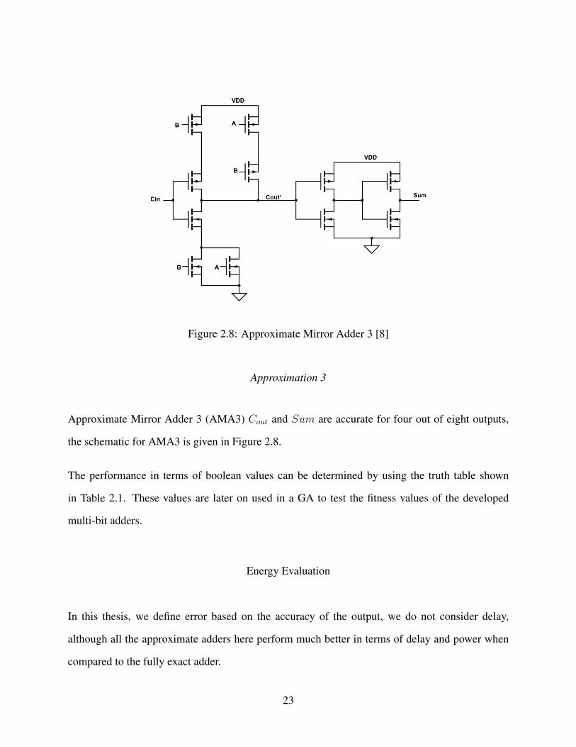
Figure 2.8: Approximate Mirror Adder 3 [8]
Approximation 3
Approximate Mirror Adder 3 (AMA3) Cout and Sum are accurate for four out of eight outputs,
the schematic for AMA3 is given in Figure 2.8.
The performance in terms of boolean values can be determined by using the truth table shown
in Table 2.1. These values are later on used in a GA to test the fitness values of the developed
multi-bit adders.
Energy Evaluation
In this thesis, we define error based on the accuracy of the output, we do not consider delay,
although all the approximate adders here perform much better in terms of delay and power when
compared to the fully exact adder.
23

Figure 2.9: Approximate Mirror Adder 4 [8]
Table 2.1: Truth Table for Conventional Full Adder and Approximations 1, 2 and 3 [7]
Inputs Accurate Outputs Approximate OutputsA B Cin Sum Cout Sum1 Cout1 Sum2 Cout2 Sum3 Cout3
0 0 0 0 0 1 0 0 0 0 00 0 1 1 0 1 0 1 0 0 00 1 0 1 0 0 1 0 0 1 00 1 1 0 1 0 1 1 0 1 01 0 0 1 0 1 0 0 1 0 11 0 1 0 1 0 1 0 1 0 11 1 0 0 1 0 1 0 1 1 11 1 1 1 1 0 1 1 1 1 1
The dynamic power dissipation of the system is given by equation (7) and the static power dis-
sipation is given by equation (8). Although power dissipation is not explicitly used in evaluation
it enables us to understand where the transistors could be removed to maximize power savings.
Additionally dynamic power dissipation which is currently gaining prominence in academia can
24

be considered in addition to static power consumption for the approximation of the circuits.
PD = Cpd ∗ V 2CC ∗ fI ∗NSW (2.1)
Where,
PD is the dynamic power consumption
VCC is the supply voltage
fI is the input signal frequency
NSW is the number of bits switching
Cpd = dynamic power-dissipation capacitance The total static power consumption of this device
can be given as:
PS = VCC ∗ Ileakage (2.2)
Where,
PS is the static power consumption
VCC is the supply voltage
Ileakage is the current into a device (sum of leakage currents)
From, equation 2.1 and 2.2, we can derive equation 2.3,
PT = Σ(PD + PS) (2.3)
The next factor we consider is the average propagation delay of an adder which is given in equation
(2.4).
25
tp =tPHL + tPLH
2(2.4)
Where,
tPHL is the time delay from High to Low
tPHL is the time delay from Low to High
In chapter 2 we discuss previous work associated with the experiments performed in this thesis.
We also discuss the various formulas used in the analysis of the performance of the approximate
adders developed in this thesis and other related works.
26
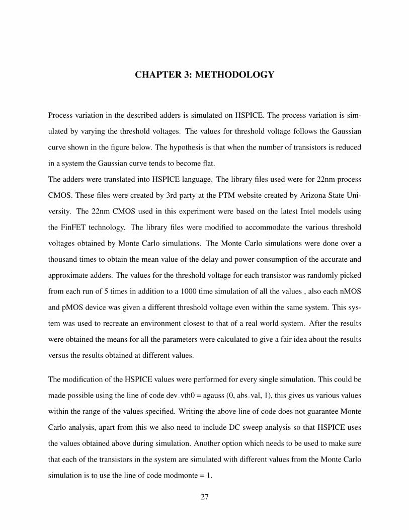
CHAPTER 3: METHODOLOGY
Process variation in the described adders is simulated on HSPICE. The process variation is sim-
ulated by varying the threshold voltages. The values for threshold voltage follows the Gaussian
curve shown in the figure below. The hypothesis is that when the number of transistors is reduced
in a system the Gaussian curve tends to become flat.
The adders were translated into HSPICE language. The library files used were for 22nm process
CMOS. These files were created by 3rd party at the PTM website created by Arizona State Uni-
versity. The 22nm CMOS used in this experiment were based on the latest Intel models using
the FinFET technology. The library files were modified to accommodate the various threshold
voltages obtained by Monte Carlo simulations. The Monte Carlo simulations were done over a
thousand times to obtain the mean value of the delay and power consumption of the accurate and
approximate adders. The values for the threshold voltage for each transistor was randomly picked
from each run of 5 times in addition to a 1000 time simulation of all the values , also each nMOS
and pMOS device was given a different threshold voltage even within the same system. This sys-
tem was used to recreate an environment closest to that of a real world system. After the results
were obtained the means for all the parameters were calculated to give a fair idea about the results
versus the results obtained at different values.
The modification of the HSPICE values were performed for every single simulation. This could be
made possible using the line of code dev vth0 = agauss (0, abs val, 1), this gives us various values
within the range of the values specified. Writing the above line of code does not guarantee Monte
Carlo analysis, apart from this we also need to include DC sweep analysis so that HSPICE uses
the values obtained above during simulation. Another option which needs to be used to make sure
that each of the transistors in the system are simulated with different values from the Monte Carlo
simulation is to use the line of code modmonte = 1.
27
Figure 3.1: Gaussian uniform distribution
Once the circuit is translated into HSPICE code and all the Monte Carlo simulations are performed
the .lis files obtained from the simulation are used to obtain the values for delays for Sum and
Carry. The .lis file also contains the mean values of the 1000 Monte Carlo simulations performed.
The number 1000 was chosen to give us a statistical probability of matching the real world setup
at 99.9%. The mean values are noted down, along with the calculated sigma values, these values
are then analyzed to determine if they conform to our hypothesis.
Experimental Results
The GA used to find the optimal solution is entirely written in C++. The program takes its input
from a .txt file generated from another program. The other program is standalone and does not
depend on the main program. This secondary program is used to generate the truth table which
is used as input to the main program. This program can produce truth tables of varying lengths
28
depending on the input bit-width. This program is used because it would be a tedious process to
create the truth table on a 8 bit adder manually.
The program used here tries to mimic an FPGAs architecture which includes CLBs, LUTs etc. The
GA constructs its chromosome from the available resources, and the original population is instan-
tiated, with each LUT assigned to a random individual. The LUT in the program is instantiated
as a class, within another class. Each LUT object consists of three vectors and a variable to store
its function type. The vectors of the LUT object map its outputs and inputs , all of the inputs and
outputs are binary values.
The LUT class is in turn instantiated in the individual class, the other vectors store the input and
output values. The function CalculateFitness calculates the fitness of the individual by going
through each LUT and compares the port values to the value given in the input golden truth table.
the fitness value is incremented by one for each value matching the original golden output. For
example, an individual representing a circuit with y inputs and x outputs will have a maximum
fitness value of 2y ∗ x. If the fitness of the individual is at a maximum, it indicates that all the
outputs of the individual are perfect. The individual class is not the primary class, it is superseded
by a larger class called the generation class.
The generation class contains the current population of individuals. The generation class consists
of a Crossover function, depending on the prescribed rate of crossover, it selects two individuals
at random and randomly picks a crossover point in a way that the LUT objects are not violated.
The LUTs before the crossover point are from Parent A and beyond the point are from Parent B.
If the crossover fails to take place due to some random chance, either one of the individuals is
directly copied on to the next generation.
29
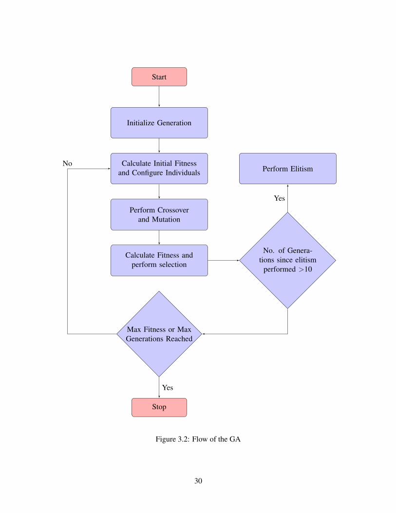
Start
Initialize Generation
Calculate Initial Fitnessand Configure Individuals
Perform Crossoverand Mutation
Calculate Fitness andperform selection
No. of Genera-tions since elitism
performed >10
Perform Elitism
Max Fitness or MaxGenerations Reached
Stop
Yes
Yes
No
Figure 3.2: Flow of the GA
30

Figure 3.3: Crossover Operation
The next function, Mutation, performs a random mutation on an individual. The function chooses
an individual and based on the user-defined mutation rate, assigns it a randomly chosen entity.
Interconnection mutation wasn’t performed because the Adders especially Ripple Carry Adders,
which take their input from the previous single-bit adders do not form recognizable circuits when
interconnections are randomly switched.
The Selection function randomly selects a defined number of individuals from the original parent
population and the evolved offspring population. The individual with the highest fitness is moved
directly to the next generation of individuals, irrespective if it was from parent generation or off-
spring generation. This process is repeated until the user-defined size of the generation is reached.
The DelayedElitism function performs elitism every 10 generations to pick the best individual
and stores it in a designated object for elite individual.
31
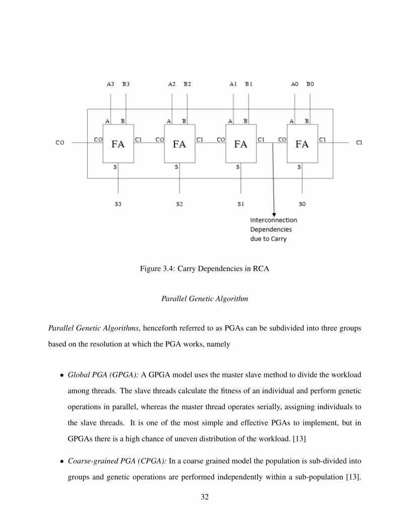
Figure 3.4: Carry Dependencies in RCA
Parallel Genetic Algorithm
Parallel Genetic Algorithms, henceforth referred to as PGAs can be subdivided into three groups
based on the resolution at which the PGA works, namely
• Global PGA (GPGA): A GPGA model uses the master slave method to divide the workload
among threads. The slave threads calculate the fitness of an individual and perform genetic
operations in parallel, whereas the master thread operates serially, assigning individuals to
the slave threads. It is one of the most simple and effective PGAs to implement, but in
GPGAs there is a high chance of uneven distribution of the workload. [13]
• Coarse-grained PGA (CPGA): In a coarse grained model the population is sub-divided into
groups and genetic operations are performed independently within a sub-population [13].
32
This type of PGA introduces a new function Migration. Migration defines the rate at which
individuals from one group move from one sub-population to another sub-population.
• Fine-Grained PGA (FGPGA): FGPGA assigns each individual to a thread and this individual
interacts with another individual within a hamming distance of 1. This type of PGA could
maintain diversity based on the neighborhood chosen. [13]
We implement a GA with three different modules: (1) Evolution of the circuit, (2) Selection of
the offspring, and (3) maximum fitness calculation as shown in Figure 5. Each module consists
of a for loop which loops through Look Up Tables (LUT) assigning different functionalities to
each LUT based on a random number between zero to four each corresponding to AMA 1-4. The
three for loops were parallelized using Intel TBB [21] parallel for loop, also vectors were used
wherever possible to give flexibility to the program. We also used OpenMP in conjunction with the
Intel TBB library to test out how it affects performance relative to only using TBB, the outcome
of this is illustrated in the results section. The main program was already designed by [15], we
modified it to change the operation of the GA extensively. The original GA in [15] could only
design MUX decoders, we changed the functionality of this Algorithm by modifying the LUTs
used in the original program to map the different Approximate Adders as single LUTs. The LUTs
considered in this program can handle 3 inputs and 2 outputs, analogous to a full adder. The
LUTs are lowest grain level the program could go. The interconnection mutation was switched off
for these genetic operations as this resulted in the two outputs being mapped to the wrong adder
occasionally. The implemented algorithm produced designs which outperform the other adders,for
example it obtains a fitness value of up to 40 for a maximum fitness value of 48.
The program uses a hierarchical approach; first the Individuals containing CLBs were designed,
each CLB has a vector of LUTs. The individuals, CLBs and LUTs are initialized as classes as
shown in [15]. The LUT class contains a function calledCalculateOutputwhich takes in the input
33
vector to calculate the output based on the functionality chosen, this is done for each individual.
The vector of individuals are initialized based on the initial population given in the input file.
We use a master slave method to generate workloads in the program. The workload is automatically
distributed by OpenMP and Intel TBB. The compilation was done in Microsoft Visual Studio
Express 2013. With the Intel TBB Plugin attached to the source of the program, as this is needed
to parallelize the program, the number of threads to run the program is taken from an input file.
This input file contains other information such as number of Configuration Logic Blocks (CLBs),
number of Look Up Tables, number of LUT select Lines, number of LUT output lines, number
of circuit input lines, number of circuit output lines, population size, mutation rate, crossover rate,
number of elite individuals, number of generations, number of threads and number of runs.
Number of CLBs
This defines the number of Configurable Logic Blocks to be used in the simulation of GA.
Number of LUTs
This defines the number of Look Up Tables to be used in the simulation of GA.
Number of LUT select lines
This defines the number of Select Lines in each LUT to be used in the simulation of GA.
Number of LUT output lines
This defines the number of outputs in each LUT to be used in the simulation of GA.
Number of Circuit Input lines
This defines the total number of input lines for the entire circuit to be developed by the GA.
Number of Circuit Input lines
This defines the total number of input lines for the entire circuit to be developed by the GA.
34
Number of Circuit Output lines
This defines the total number of output lines for the entire circuit to be developed by the GA.
Population Size
This defines the total number of individuals initialized at the start of the GA.
Crossover Rate
This defines the probability at which two parents would be crossed over to produce offspring.
If crossover does not happen then the parents are directly copied to the next generation.
Mutation Rate
This defines the probability at which mutation would take place after the crossover is done.
Number of Generations
This defines the number of generations at which the simulation stops
Number of Threads
This defines the number of cores/threads to be used when the simulation is running
Number of Runs
This defines the number of times the simulation needs to be run.
In this chapter we identified the various dependencies in the Ripple Carry Adders and Carry Looka-
head Adders and mapped them to the GA. These dependencies if not taken into account cannot be
simulated on a computer program.
For Parallel GAs we looked at a number of API’s including POSIX, OpenMP and Intel TBB along
with their overheads when they are implemented. From the analysis we can conclude that although
OpenMP and Intel TBB provide coarse grain control over multi-threading, they remove the burden
35

of the programmer to manually divide the tasks among threads, whereas OpenMP and Intel TBB
do this automatically with greater efficiency.
36
CHAPTER 4: EXPERIMENTAL RESULTS
The four approximate mirror adders and the accurate adder were analyzed using HSPICE . Apart
from simulation of process variation the adders were also subjected to varying Vdd voltages rang-
ing from 0.65V to 0.8V (Nominal Voltage). The analysis was done on worst case scenarios where
all the inputs were ones. In certain cases, the delay was not available because the output would
not rise in such cases the inputs with the most number of ones which yielded an appropriate output
such that the output delay could be measured. The results obtained for various adders are tabulated
and explained here.
As VTH variation does not affect all the Approximate Adders equally, then one of the ideas which
can be implemented is logic diversity. Logic diversity involves using different sets of systems to
gain the best overall performance.
In this case a GA could be used to involve a search space to determine which adders could perform
best in a certain scenario. It is not always necessary for similar adders in a system to perform better
than different types of adders in a system. For e.g. in a 16 bit Adder AMA-I and AMA-II may
perform better in cases of DSP applications, but when only approximate calculations are required
then a 16 bit adder containing solely AMA-I may perform better. In [22] soft resiliency has been
mentioned, which can be defined as the property of a system to gracefully degrade the quality of
the output as the components of a system malfunction. For a system to gracefully degrade, the
system would require an underlying GA to perform an analysis of the search space and assign
fitness value to each component during runtime. The fitness values can then be used to identify
functioning components and use them instead of the malfunctioning items. Another method would
be to use a partially malfunctioning LUT as an approximate gate. This could be especially useful
in DSP applications where the loss of quality cannot be distinguished by humans.
37
RCA Adders
Table 4.1: Results of Accurate Mirror Adder
Voltage Sum Carry Sum Carry Sum Carry Sum CarryWorst Worst Mean Mean Variance Variance Sigma Sigma
0.8 148ps 58.09ps 131.46ps 43.41ps 8.36E-23 4.78E-23 9.14ps 6.91ps
0.75 152.8ps 66.04ps 133.82ps 48.76ps 1.05E-22 6.03E-23 10.24ps 7.63ps
0.7 160.4ps 79.45ps 138.48ps 55.61ps 1.52E-22 8.04E-23 12.32ps 8.96ps
0.65 173.3p 103.4p 145.1ps 65.83ps 2.83E-22 1.25E-22 16.81ps 11.19ps
Multi-bit approximate adder circuits are designed using the proposed methodology. Other bench-
marks can also be designed if the multiple versions of approximate designs are available. For the
benchmark utilized, the maximum fitness of the circuit is dependent on the number of inputs n and
is equal to 2n+1.
Table 4.2: Results of Approximate Mirror Adder I
Voltage Sum Carry Sum Carry Sum Carry Sum CarryWorst Worst Mean Mean Variance Variance Sigma Sigma
0.8 49.04ps 37.54ps 31.33ps 20.77ps 4.59E-23 6.83E-23 8.26ps 6.77ps
0.75 55.84ps 43.06ps 36.32ps 25.26ps 5.73E-23 8.35E-23 9.15ps 7.56ps
0.7 66.69ps 48.93ps 42.5ps 30.8ps 6.83E-23 1.08E-22 10.4ps 8.26ps
0.65 87.47ps 56.99ps 50.79ps 37.41ps 8.07E-23 1.85E-22 13.58ps 8.98ps
The GA was executed for a maximum of 5000 generations with a population size of 20 circuits con-
sisting of randomly instantiated individuals. The GA selects a random set of individuals (parents)
from the population after which tbb evolve is invoked which evolves the circuit in parallel, which
is followed by tbb postselect and maxfit which are the processes for selecting the offspring and
38
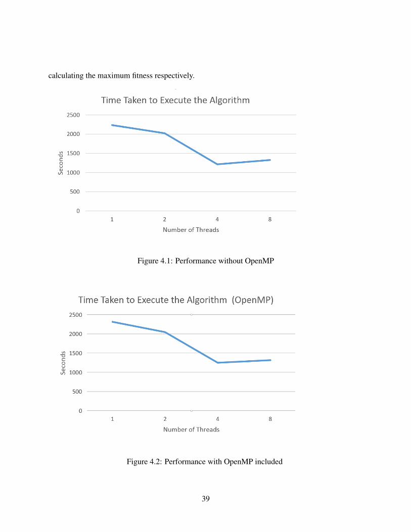
calculating the maximum fitness respectively.
Figure 4.1: Performance without OpenMP
Figure 4.2: Performance with OpenMP included
39
One of the important observations was that the GA took as much time to evolve as to calculate the
fitness, sometimes the time to evolve was greater than the time to calculate the fitness. This is a
context-dependent observation as the time to evolve or to calculate the fitness values depends on
the complexity of the calculation within each function.
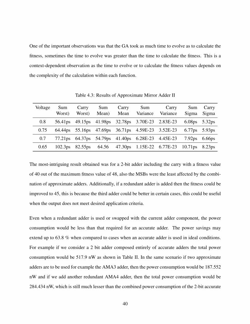
Table 4.3: Results of Approximate Mirror Adder II
Voltage Sum Carry Sum Carry Sum Carry Sum CarryWorst) Worst) Mean) Mean Variance Variance Sigma Sigma
0.8 56.41ps 49.15ps 41.98ps 32.78ps 3.70E-23 2.83E-23 6.08ps 5.32ps
0.75 64.44ps 55.16ps 47.69ps 36.71ps 4.59E-23 3.52E-23 6.77ps 5.93ps
0.7 77.21ps 64.37ps 54.79ps 41.40ps 6.28E-23 4.45E-23 7.92ps 6.66ps
0.65 102.3ps 82.55ps 64.56 47.30ps 1.15E-22 6.77E-23 10.71ps 8.23ps
The most-intriguing result obtained was for a 2-bit adder including the carry with a fitness value
of 40 out of the maximum fitness value of 48, also the MSBs were the least affected by the combi-
nation of approximate adders. Additionally, if a redundant adder is added then the fitness could be
improved to 45, this is because the third adder could be better in certain cases, this could be useful
when the output does not meet desired application criteria.
Even when a redundant adder is used or swapped with the current adder component, the power
consumption would be less than that required for an accurate adder. The power savings may
extend up to 63.8 % when compared to cases when an accurate adder is used in ideal conditions.
For example if we consider a 2 bit adder composed entirely of accurate adders the total power
consumption would be 517.9 nW as shown in Table II. In the same scenario if two approximate
adders are to be used for example the AMA3 adder, then the power consumption would be 187.552
nW and if we add another redundant AMA4 adder, then the total power consumption would be
284.434 nW, which is still much lesser than the combined power consumption of the 2-bit accurate
40
adders.
Table 4.4: Results of Approximate Mirror Adder III
Voltage Sum Carry Sum Carry Sum Carry Sum CarryWorst Worst Mean Mean Variance Variance Sigma Sigma
0.8 59.39ps 51.09ps 43.68ps 34.32ps 3.62E-23 3.76E-23 6.01ps 6.13ps
0.75 68.01ps 57.09ps 49.5ps 38.37ps 4.67E-23 4.72E-23 6.83ps 6.86ps
0.7 82.28ps 66.75ps 56.90ps 43.19ps 6.80E-23 6.00E-23 8.24ps 7.74ps
0.65 106.5 86.2 67.39ps 49.46ps 1.30E-22 9.22E-23 11.40ps 9.60ps
Execution times for the design of approximate adders with and without OpenMP are shown in
Figures 6 and 7 respectively. A speed-up of about 1.61-fold using four threads is achieved on a
quad-core processor, which is far less than linear. A speedup of at least two on four threads would
have been promising. We believe this could be possible with the introduction of larger generation
gap in Delayed Elitism.
Table 4.5: Results of Approximate Mirror Adder IV
Voltage Sum Carry Sum Carry Sum Carry Sum CarryWorst Worst Mean Mean Variance Variance Sigma Sigma
0.8 151.1ps 27.36ps 137.21ps 14.29ps 3.13E-23 4.59E-23 5.59ps 6.77ps
0.75 157.5ps 31.8ps 141.74ps 17.3287ps 3.95E-23 5.83E-23 6.29ps 7.64ps
0.7 167.2ps 37.29ps 147.38ps 21.15ps 5.71E-23 7.37E-23 7.56ps 8.59ps
0.65 184.8ps 42.85ps 155.41ps 25.81ps 1.15E-22 9.07E-23 10.7ps 9.54ps
When mutation was introduced in interconnections between LUTs, the developed circuit did not
match the required configuration; the interconnections are important, as in a multiple bit adder, it
is required for single bit adders to be in sequence so that the carry is propagated appropriately. The
41
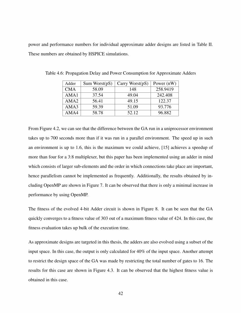
power and performance numbers for individual approximate adder designs are listed in Table II.
These numbers are obtained by HSPICE simulations.
Table 4.6: Propagation Delay and Power Consumption for Approximate Adders
Adder Sum Worst(pS) Carry Worst(pS) Power (nW)CMA 58.09 148 258.9419AMA1 37.54 49.04 242.408AMA2 56.41 49.15 122.37AMA3 59.39 51.09 93.776AMA4 58.78 52.12 96.882
From Figure 4.2, we can see that the difference between the GA run in a uniprocessor environment
takes up to 700 seconds more than if it was run in a parallel environment. The speed up in such
an environment is up to 1.6, this is the maximum we could achieve, [15] achieves a speedup of
more than four for a 3:8 multiplexer, but this paper has been implemented using an adder in mind
which consists of larger sub-elements and the order in which connections take place are important,
hence parallelism cannot be implemented as frequently. Additionally, the results obtained by in-
cluding OpenMP are shown in Figure 7. It can be observed that there is only a minimal increase in
performance by using OpenMP.
The fitness of the evolved 4-bit Adder circuit is shown in Figure 8. It can be seen that the GA
quickly converges to a fitness value of 303 out of a maximum fitness value of 424. In this case, the
fitness evaluation takes up bulk of the execution time.
As approximate designs are targeted in this thesis, the adders are also evolved using a subset of the
input space. In this case, the output is only calculated for 40% of the input space. Another attempt
to restrict the design space of the GA was made by restricting the total number of gates to 16. The
results for this case are shown in Figure 4.3. It can be observed that the highest fitness value is
obtained in this case.
42
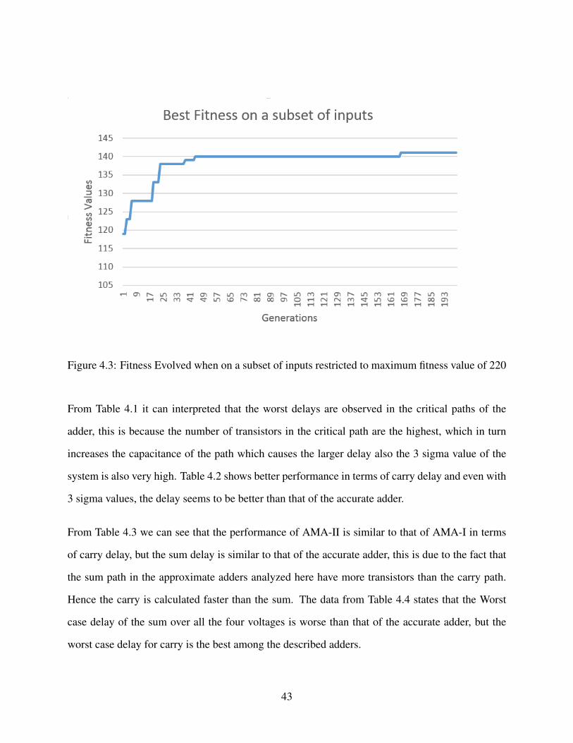
Figure 4.3: Fitness Evolved when on a subset of inputs restricted to maximum fitness value of 220
From Table 4.1 it can interpreted that the worst delays are observed in the critical paths of the
adder, this is because the number of transistors in the critical path are the highest, which in turn
increases the capacitance of the path which causes the larger delay also the 3 sigma value of the
system is also very high. Table 4.2 shows better performance in terms of carry delay and even with
3 sigma values, the delay seems to be better than that of the accurate adder.
From Table 4.3 we can see that the performance of AMA-II is similar to that of AMA-I in terms
of carry delay, but the sum delay is similar to that of the accurate adder, this is due to the fact that
the sum path in the approximate adders analyzed here have more transistors than the carry path.
Hence the carry is calculated faster than the sum. The data from Table 4.4 states that the Worst
case delay of the sum over all the four voltages is worse than that of the accurate adder, but the
worst case delay for carry is the best among the described adders.
43
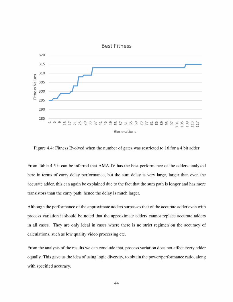
Figure 4.4: Fitness Evolved when the number of gates was restricted to 16 for a 4 bit adder
From Table 4.5 it can be inferred that AMA-IV has the best performance of the adders analyzed
here in terms of carry delay performance, but the sum delay is very large, larger than even the
accurate adder, this can again be explained due to the fact that the sum path is longer and has more
transistors than the carry path, hence the delay is much larger.
Although the performance of the approximate adders surpasses that of the accurate adder even with
process variation it should be noted that the approximate adders cannot replace accurate adders
in all cases. They are only ideal in cases where there is no strict regimen on the accuracy of
calculations, such as low quality video processing etc.
From the analysis of the results we can conclude that, process variation does not affect every adder
equally. This gave us the idea of using logic diversity, to obtain the power/performance ratio, along
with specified accuracy.
44
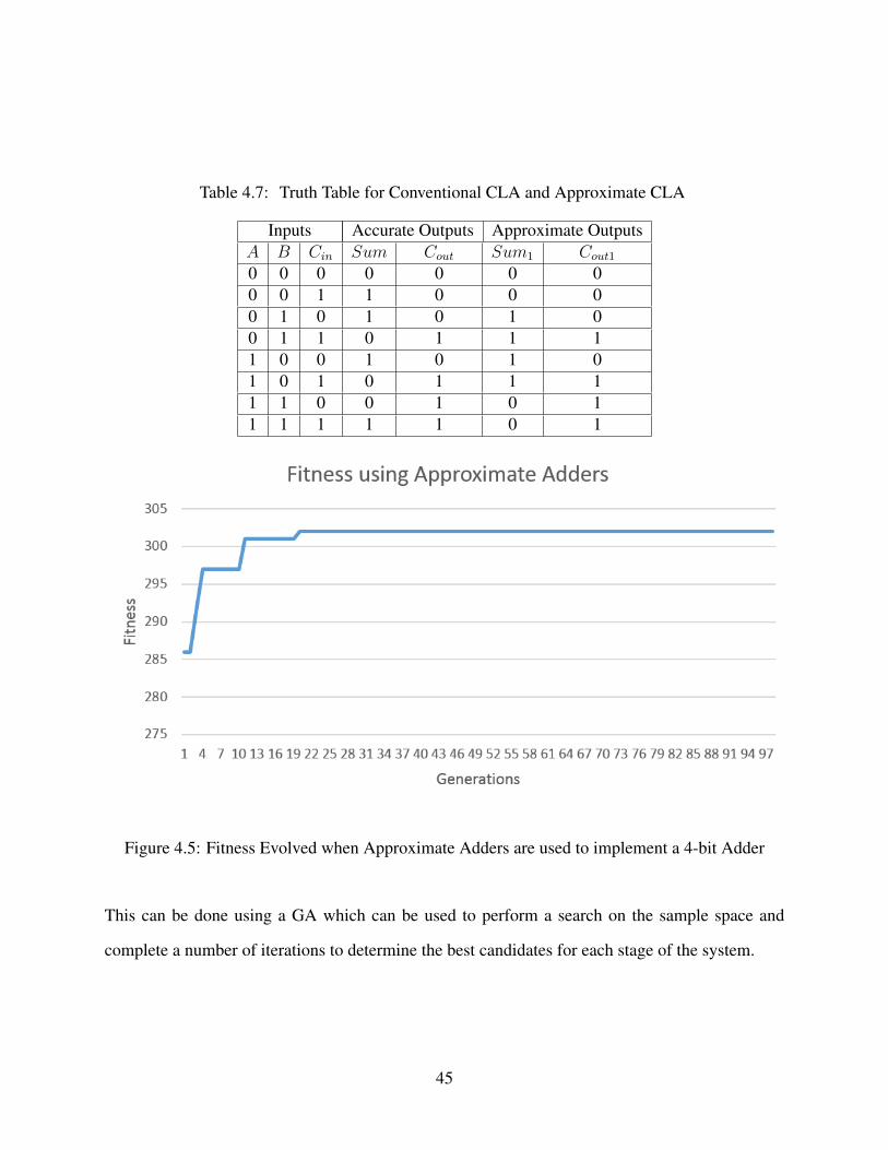
Table 4.7: Truth Table for Conventional CLA and Approximate CLA
Inputs Accurate Outputs Approximate OutputsA B Cin Sum Cout Sum1 Cout1
0 0 0 0 0 0 00 0 1 1 0 0 00 1 0 1 0 1 00 1 1 0 1 1 11 0 0 1 0 1 01 0 1 0 1 1 11 1 0 0 1 0 11 1 1 1 1 0 1
Figure 4.5: Fitness Evolved when Approximate Adders are used to implement a 4-bit Adder
This can be done using a GA which can be used to perform a search on the sample space and
complete a number of iterations to determine the best candidates for each stage of the system.
45
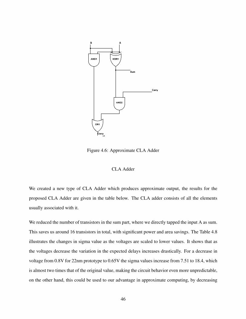
Figure 4.6: Approximate CLA Adder
CLA Adder
We created a new type of CLA Adder which produces approximate output, the results for the
proposed CLA Adder are given in the table below. The CLA adder consists of all the elements
usually associated with it.
We reduced the number of transistors in the sum part, where we directly tapped the input A as sum.
This saves us around 16 transistors in total, with significant power and area savings. The Table 4.8
illustrates the changes in sigma value as the voltages are scaled to lower values. It shows that as
the voltages decrease the variation in the expected delays increases drastically. For a decrease in
voltage from 0.8V for 22nm prototype to 0.65V the sigma values increase from 7.51 to 18.4, which
is almost two times that of the original value, making the circuit behavior even more unpredictable,
on the other hand, this could be used to our advantage in approximate computing, by decreasing
46

the voltage and reducing the time required to latch on to the values could lead to interesting results.
Figure 4.7: Accurate CLA Adder
Table 4.8: Results of Approximate CLA
Voltage Sum Carry Sum Carry Sum Carry Sum CarryWorst Worst Mean Mean Variance Variance Sigma Sigma
0.8 0 64.22ps 0 36.8215ps 0.00E+00 5.64E-23 0 7.51ps
0.75 0 81.59ps 0 47.0368ps 0.00E+00 8.50E-23 0 9.2181ps
0.7 0 119.3ps 0 61.5858ps 0.00E+00 1.49E-22 0 12.1989ps
0.65 0 199.5ps 0 83.8076ps 0.00E+00 3.39E-22 0 18.4029ps
There could be other areas to approximate in this type of adder, especially the carry propagation
47

part, which increases with complexity as the number of computation bits increase, but modifying
the carry part could lead to changes in the carry output, as carry usually amounts to MSB, the
output could be severely compromised even for small changes, which could not be satisfactory as
the power saved would not be proportional to the accuracy lost.
48

CHAPTER 5: CONCLUSION
This thesis indicates benefit for parallelizing the GA and exploration of creative cascaded circuits
such as adders where the current stage is heavily-dependent on the previous stage. Although
we were able to achieve a modest speed-up of 1.61, in most cases, when the population size is
increased then the effects of parallelization tends to be more pronounced.
Future work could include implementation of DelayedElitism which could improve the avenues
where parallelism could be improved, in case of DelayedElitism the parallel invoke method in
TBB could be used to run fitness evaluation function and Evolution in parallel, this could improve
the design-time significantly. Also, the GA could be modified to design larger circuits than the
ones currently designed, these could then be implemented in chips where manual intervention for
hardware faults is not possible, in such cases a GA could be remotely used to reconfigure the
circuits when the systems aren’t functioning appropriately.
The effect of process variation was also calculated. As the number of transistors is reduced, the
distribution of the transistor widths and gate oxide may shift away from a Gaussian Curve. This
result was demonstrated in different types of single-bit adders with the delay sigma increasing
from 6psec to 12psec, and when the voltage is scaled to Near-Threshold-Voltage (NTV) levels the
sigma increases by up to 5psec. Approximate Arithmetic Units were not affected more greatly by
the change in distribution of the thickness of the gate oxide. Even when considering the 3-sigma
value, the delay of an approximate adder remains below that of a precise adder with additional
transistors. Additionally, it is demonstrated that the GA obtains innovative solutions to the ap-
propriate combination of approximate arithmetic units, to achieve a good balance between energy
savings and accuracy.
49
In the future, further enhancements could be implemented. Including testing out the 10nm FinFET
as well as the 7nm FinFET which is currently on the road-map for Intel, as the sizes move towards
the lower end the effect of process variation could be more pronounced in approximate circuits,
but the current generation of transistors used in approximate adders have minimal effect on the
performance of such adders.
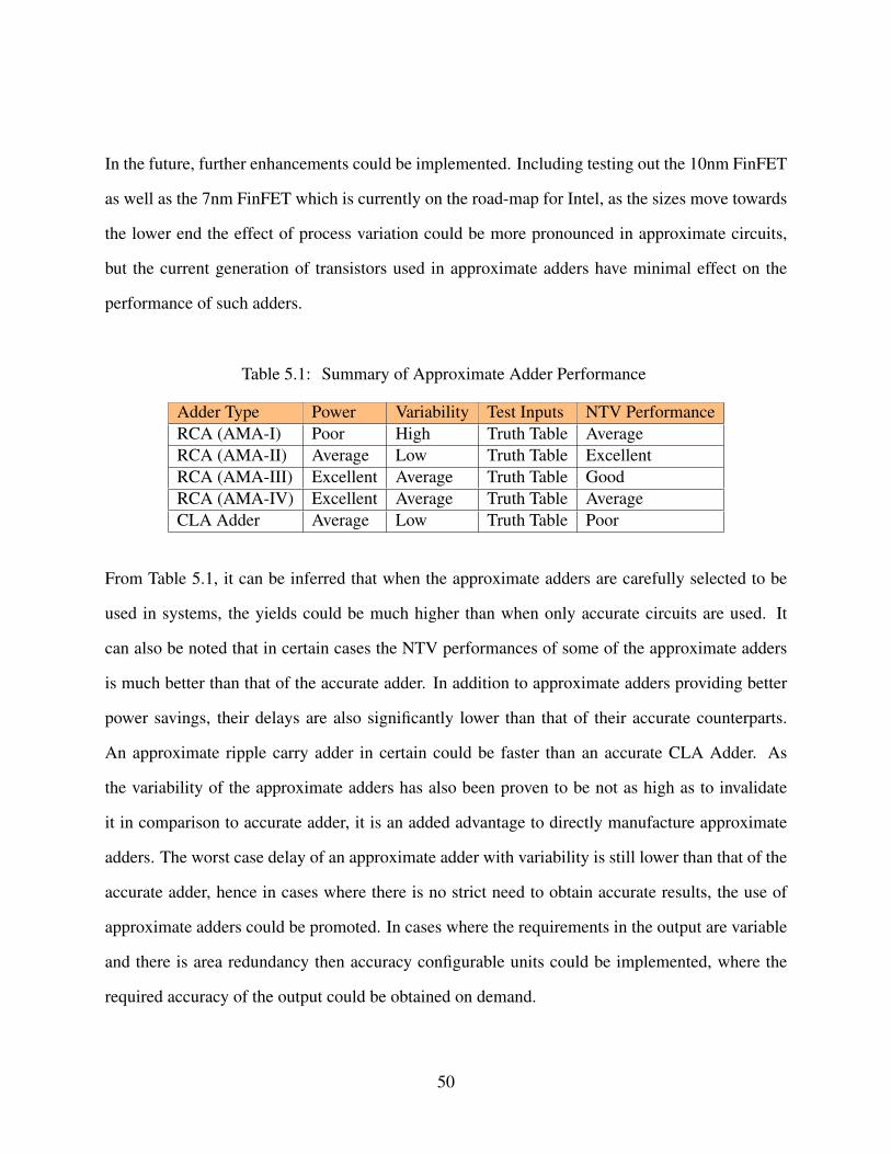
Table 5.1: Summary of Approximate Adder Performance
Adder Type Power Variability Test Inputs NTV PerformanceRCA (AMA-I) Poor High Truth Table AverageRCA (AMA-II) Average Low Truth Table ExcellentRCA (AMA-III) Excellent Average Truth Table GoodRCA (AMA-IV) Excellent Average Truth Table AverageCLA Adder Average Low Truth Table Poor
From Table 5.1, it can be inferred that when the approximate adders are carefully selected to be
used in systems, the yields could be much higher than when only accurate circuits are used. It
can also be noted that in certain cases the NTV performances of some of the approximate adders
is much better than that of the accurate adder. In addition to approximate adders providing better
power savings, their delays are also significantly lower than that of their accurate counterparts.
An approximate ripple carry adder in certain could be faster than an accurate CLA Adder. As
the variability of the approximate adders has also been proven to be not as high as to invalidate
it in comparison to accurate adder, it is an added advantage to directly manufacture approximate
adders. The worst case delay of an approximate adder with variability is still lower than that of the
accurate adder, hence in cases where there is no strict need to obtain accurate results, the use of
approximate adders could be promoted. In cases where the requirements in the output are variable
and there is area redundancy then accuracy configurable units could be implemented, where the
required accuracy of the output could be obtained on demand.
50
The comparison of OpenMP and Intel TBB is also done here. The results show that OpenMP is
slightly faster than Intel TBB on eight threads, but it is not faster by a significant amount. This
result could also be due to the workload of the CPU at any given time. Under certain circumstances
when the OS is using up more resources, the allocation of work could become a bit skewed, this
could result in different results when the number of threads is greater than the number of cores,
but we repeated the experiment a number of times to obtain this result. It can also be confidently
said that under normal circumstances when the APIs OpenMP and Intel TBB are used when the
number of threads is equal to the number of cores available on the machine. This is due the fact that
when the number of threads is greater than the number of cores the data is assigned in a random
order over four cores, which causes slight overhead due to assignment of data in the pipeline.
The methods of parallelizing either way is also different, the OpenMP concept uses barriers and
pragmas to implement parallelism whereas Intel TBB uses a method which is also used in POSIX
implementation i.e. it uses functions as a way of implementing parallelism. The functions are then
appropriately multiplied and assigned to different threads automatically.
Future work could include implementation of a GA which could also perform HSPICE simulations
to calculate its fitness value and use the results from the HSPICE simulation to determine the
correct circuit to be implemented. This could be parallelized by running multiple instances of
HSPICE. The main issue with such an implementation would be the ability of the simulation
environment to create a netlist and to make sure that any netlist produced by such an environment
follows the rules of HSPICE syntax with a high degree accuracy, the other challenge would be
obtain the results from the output of HSPICE, this should be easier than generating the netlist, as
the output usually contains the results after a certain keyword. Hence the environment could be
programmed to perform a keyword search to find the required results. The third major issue with
such a setup would be the time required to perform a fitness calculation, with a sample of 1000
51

Monte Carlo simulations, the simulation on HSPICE of any sizable circuit would be greater than
5 hours depending on the processing power of the machine used. If these challenges were to be
solved a feasible GA could be made, which could make highly efficient circuits on demand.
52
APPENDIX : SIMULATION CODE
53
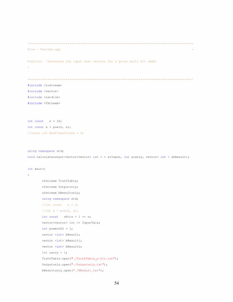
/******************************************************************************************
File - TestGen.cpp *
*
Function - Generates the input test vectors for a given multi bit adder
*
*
******************************************************************************************/
#include <iostream>
#include <vector>
#include <cstdlib>
#include <fstream>
int const n = 16;
int const x = pow(2, n);
//const int NoofInputLines = 4;
using namespace std;
void calculateoutput(vector<vector< int > > &vInput, int &carry, vector< int > &bResult);
int main()
{
ofstream TruthTable;
ofstream Outputonly;
ofstream bResultonly;
using namespace std;
//int const n = 4;
//int x = pow(2, n);
int const nBits = 1 << n;
vector<vector< int >> InputVals;
int powerOf2 = 1;
vector <int> bResult;
vector <int> bResult1;
vector <int> bResult2;
int carry = 1;
TruthTable.open("./TruthTable n-bit.txt");
Outputonly.open("./Outputonly.txt");
bResultonly.open("./BResult.txt");
54
int counter = 0;
int loopCounter = n / 2 - 1;
for (int i = 0; i < n; ++i)
{
InputVals.push_back(vector < int >());
for (int bitNum = 0; bitNum < nBits; ++bitNum)
{
//cout << 1 - bitNum / powerOf2 % 2;
InputVals.at(i).push_back(1 - bitNum / powerOf2 % 2);
cout << InputVals.at(i).at(bitNum);
//cout << " ";
}
cout << endl;
powerOf2 *= 2;
}
calculateoutput(InputVals, carry, bResult);
/*for (int i = x*2 - 2 ; i >= 0 ; i= i - 2)
{
bResult2.push_back(bResult[i]);
}
for (int i = x*2 - 1; i >= 0; i = i - 2)
{
bResult1.push_back(bResult[i]);
}*/
//InputVals.insert(InputVals.begin(),bResult);
//InputVals.insert(InputVals.begin(), bResult2);
//cout << bResult.size();
55
//InputVals.push_back(bResult1);
//InputVals.push_back(bResult2);
// for (i = 0; i)
for (int j = x - 1; j >= 0; j--)
{
for (int i = n - 1; i >= 0; i = i--)
{
//cout << InputVals.at(i).at(j) << " ";
TruthTable << InputVals.at(i).at(j) << " ";
}
//cout << InputVals.at(i).at(j + 1);
for (int i = loopCounter; i >= (loopCounter - n/2 - 1) ; i--)
{
counter++;
cout << counter << endl;
cout << loopCounter << endl;
if (counter >= n / 2 )
{
cout << " "<< bResult[i] << " ";
TruthTable << bResult[i] << " ";
Outputonly << bResult[i] << " ";
loopCounter += counter;
counter = 0;
break;
}
if (loopCounter > x*n)
break;
//cout << bResult[i] << " ";
TruthTable << bResult[i] << " ";
Outputonly << bResult[i] << " ";
}
56

cout << endl;
TruthTable << endl;
}
for (int i = 0; i < x * 2 - 1; i++)
bResultonly << bResult[i] << " ";
cout << bResult.size();
TruthTable.close();
Outputonly.close();
bResultonly.close();
system("pause");
}
/******************************************************************************************
File - SPFit.cpp
Function - Makes the TestGen output readable for the Main Program
******************************************************************************************/
# include<stdio.h>
# include<iostream>
#include <fstream>
#include <vector>
#include <string>
using namespace std;
void main()
{
int inputs;
ifstream input;
ofstream output;
char temp[256];
string pushed[1000];
input.open("./FPGA.txt");
output.open("./Output.txt");
57

if (!input)
{
cerr << "Couldn’t Open the Settings File" << endl;
}
for (int j = 0; j < 120; j++)
{
//for (int i = 0; i < 5; i++)
{
input >> inputs;
input.getline(temp,255);
pushed[j] = temp;
cout << pushed[j].size();
}
}
cout << pushed[0][4];
for (int j = 0; j < 120; j++)
{
for (int i = 1; i < 4; i++)
{
output << pushed[j][i];
}
output << endl;
}
output.close();
input.close();
system("pause");
}
58
/******************************************************************************************
File - DataStructures.h
Function - Provides Scaffolding for the main loop
******************************************************************************************/
#include <vector>
#include <string.h>
#include <fstream>
#include <iostream>
#include <math.h>
#include <time.h>
#include "tbb/parallel_for.h"
#include "tbb/blocked_range.h"
#include "tbb/concurrent_vector.h"
#include "tbb/spin_mutex.h"
#include <cstdlib>
using namespace std;
using namespace tbb;
using std::vector;
//Settings for FPGA and GA parameters
class ClsSettings
{
public:
//FPGA settings
string FilePath;//the settings input file path
int NoOfCLBs;
int NoOfLUTsPerCLB;
int NoOfLUTSelectLines;
int NoOfLUTOutputLines;
int NoOfInputLines;
int NoOfOutputLines;
int nthreads; // number of threads
59
int nruns; // number of runs
//GA parameters settings
int PopulationSize;
int OffSpringSize;
float MutationRate;
float CrossoverRate;
int NoOfGenerations;
int TournamentSize;
int ElitismSize;
//Input and Output settings
int NoOfConfigFiles;
int NoOfGenerationOutput;
//Read input file and fill into the parameters above
bool ReadFile();
};
class ClsPortValue
{
public:
vector <bool> vbTruthTableInput;
vector <bool> vbTruthTableOutput;
};
/***********************************************************************************************/
//Defines the truth table inputs and outputs and reads their values from file
class ClsTruthTable
{
public:
string FilePath; //the truth table’s input file path
string ModuleName;
int NoOfInputPorts;
int NoOfOutputPorts;
int NoOfRows;
vector <ClsPortValue> vcPortValue;
//Read input file and fill values into Truth Table
60
bool ReadFile();
˜ClsTruthTable();
};
/***********************************************************************************************/
//Defines FPGA basic block unit (Look_Up_Table)
class ClsLUT
{
public:
vector <bool> vInputValue;
vector <int> vInputLine;
vector <bool> vOutputValue;
int FunctionType;
bool CalculateOutput(vector <bool>,volatile int [], int carry);
bool LutCopy(ClsLUT *, ClsLUT *, ClsSettings *);
};
/***********************************************************************************************/
//each Configurable_Logic_Block is given an ID
class ClsCLB
{
public:
vector <ClsLUT *> LUTs;//each CLB is an array of LUTs
//Functions
bool DeleteCls();
};
/***********************************************************************************************/
//Each Individual has an ID and a chromosome
class ClsIndividual
{
public:
vector <ClsCLB *> CLBS;
vector <bool> vInput;
vector <int> vOutputLine;
vector <bool> vOutputValue;
int iFitness;
bool ConfigurationIndivi(ClsSettings * Object);
61

//Generate a Boolean function randomly
int AssignBooleanFunction();
//calculates each individual’s fitness relative to the truth table output
bool CalculateFitness(ClsTruthTable * , ClsSettings *,bool );
bool ClsCleanAll();
//Does Copy operation for an individual
bool PerformCopy(ClsIndividual *,ClsSettings * );
//Output the Configuration of Individual
void ConfigOutput(ClsSettings * Object);
//Convert the function type to string
string FunctionType(int);
};
/***********************************************************************************************/
//defines a generation as a vector of individuals
class ClsGeneration
{
public:
int ID;
tbb::concurrent_vector<ClsIndividual *> Individuals;
tbb::concurrent_vector<ClsIndividual *> vOffSpring;
tbb::concurrent_vector<int> vOffSpringIndex;
//tbb::concurrent_vector<int> vSelected;
tbb::concurrent_vector<int> vIndividual;
spin_mutex FitnessMutex;
int MaxCalculatedFitness;
int iMaxIndivi;
bool InitializeGeneration(ClsSettings *);
int Selection(ClsSettings *, ClsGeneration * );
bool PerformCrossover(ClsIndividual *,ClsIndividual *,ClsIndividual *,ClsSettings *);
62
bool PerformMutation(ClsIndividual *,ClsSettings *);
bool PerformElitism(ClsIndividual *,ClsSettings *);
private:
};
/******************************************************************************************
File - Coutput.cpp
Function - Calculates the Output and compares the output with the input
******************************************************************************************/
#include "DataStructures.h"
/********AA(Note to Self) - Do Not Modify!! Checked !********/
//According to the inputs and lut functionality
//get the LUT output
bool ClsLUT::CalculateOutput (vector <bool> vInput,volatile int bResult[], int carry)
{
bool bReturn=false;
//int iIndex=0;
volatile int caser;
vInput[2] = carry;
if ((vInput[0] == 0 && vInput[1] == 0 && vInput[2] == 0))
caser = 0;
else if ((vInput[0] == 0 && vInput[1] == 0 && vInput[2] == 1))
caser = 1;
else if ((vInput[0] == 0 && vInput[1] == 1 && vInput[2] == 0))
caser = 2;
else if (vInput[0] == 0 && vInput[1] == 1 && vInput[2] == 1)
caser = 3;
else if (vInput[0] == 1 && vInput[1] == 0 && vInput[2] == 0)
caser = 4;
else if (vInput[0] == 1 && vInput[1] == 0 && vInput[2] == 1)
63
caser = 5;
else if (vInput[0] == 1 && vInput[1] == 1 && vInput[2] == 0)
caser = 6;
else if (vInput[0] == 1 && vInput[1] == 1 && vInput[2] == 1)
caser = 7;
switch (FunctionType)
{
//AMA 1
case 0:
if (vInput.size() < 3)
{
cout<< "InputSize error";
return bReturn;
exit(0);
}
// begin truth table
else
{
if (caser == 0 || caser == 4)
{
bResult[0] = 0;
bResult[1] = 0;
}
else if (caser == 1)
{
bResult[0] = 1;
bResult[1] = 0;
}
else if (caser == 2 || caser == 3 || caser == 5 || caser == 6)
{
bResult[0] = 0;
bResult[1] = 1;
}
else if (caser == 7)
{
bResult[0] = 1;
bResult[1] = 1;
64
}
}
// end truth table
break;
// Approximate Adders 2
case 1:
if (vInput.size() < 3)
{
cout<< "InputSize error";
return bReturn;
exit(0);
}
else
{
if (caser == 3 || caser == 5 || caser == 6 || caser == 7)
{
bResult[0] = 0;
bResult[1] = 1;
}
else if (caser == 0 || caser == 1 || caser == 2 || caser == 4)
{
bResult[0] = 1;
bResult[1] = 0;
}
}
bReturn=true;
break;
// Approx Adder 3
case 2:
if (vInput.size() < 3)
{
cout<< "InputSize error";
return bReturn;
exit(0);
}
65
else
{
if (caser == 0 || caser == 1 || caser == 4)
{
bResult[0] = 1;
bResult[1] = 0;
}
else if (caser == 2 || caser == 3 || caser == 5 || caser == 6 || caser == 7)
{
bResult[0] = 0;
bResult[1] = 1;
}
}
bReturn=true;
break;
// Approx Adder 4
case 3:
if (vInput.size() < 3)
{
cout<< "InputSize error";
return bReturn;
exit(0);
}
else
{
if (caser == 0 || caser == 2)
{
bResult[0] = 0;
bResult[1] = 0;
}
else if (caser == 1 || caser == 3)
{
bResult[0] = 1;
bResult[1] = 0;
}
else if (caser == 4 || caser == 5 || caser == 6)
66

{
bResult[0] = 0;
bResult[1] = 1;
}
else if (caser == 7)
{
bResult[0] = 1;
bResult[1] = 1;
}
}
bReturn=true;
break;
default:
cout << "Error in the LUT calculation function"<<endl;
bReturn=false;
break;
}
return bReturn;
}
//Copy current LUT to secondLut LUT
bool ClsLUT::LutCopy (ClsLUT * FirstLut, ClsLUT * SecondLut, ClsSettings * Settings)
{
bool bResult=true;
int iIndex=0;
SecondLut->FunctionType = FirstLut->FunctionType;
for (iIndex=0; iIndex < Settings->NoOfLUTSelectLines ; iIndex++)
{
SecondLut->vInputLine[iIndex]= FirstLut->vInputLine[iIndex];
}
return bResult;
}
67
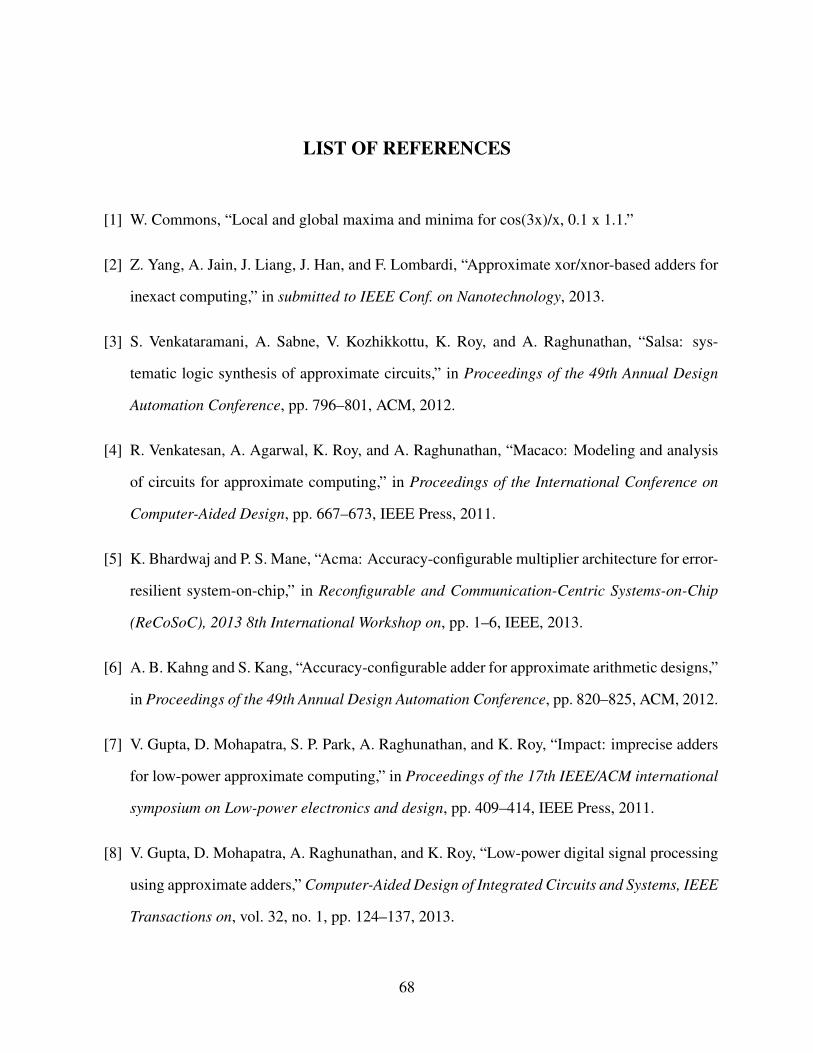
LIST OF REFERENCES
[1] W. Commons, “Local and global maxima and minima for cos(3x)/x, 0.1 x 1.1.”
[2] Z. Yang, A. Jain, J. Liang, J. Han, and F. Lombardi, “Approximate xor/xnor-based adders for
inexact computing,” in submitted to IEEE Conf. on Nanotechnology, 2013.
[3] S. Venkataramani, A. Sabne, V. Kozhikkottu, K. Roy, and A. Raghunathan, “Salsa: sys-
tematic logic synthesis of approximate circuits,” in Proceedings of the 49th Annual Design
Automation Conference, pp. 796–801, ACM, 2012.
[4] R. Venkatesan, A. Agarwal, K. Roy, and A. Raghunathan, “Macaco: Modeling and analysis
of circuits for approximate computing,” in Proceedings of the International Conference on
Computer-Aided Design, pp. 667–673, IEEE Press, 2011.
[5] K. Bhardwaj and P. S. Mane, “Acma: Accuracy-configurable multiplier architecture for error-
resilient system-on-chip,” in Reconfigurable and Communication-Centric Systems-on-Chip
(ReCoSoC), 2013 8th International Workshop on, pp. 1–6, IEEE, 2013.
[6] A. B. Kahng and S. Kang, “Accuracy-configurable adder for approximate arithmetic designs,”
in Proceedings of the 49th Annual Design Automation Conference, pp. 820–825, ACM, 2012.
[7] V. Gupta, D. Mohapatra, S. P. Park, A. Raghunathan, and K. Roy, “Impact: imprecise adders
for low-power approximate computing,” in Proceedings of the 17th IEEE/ACM international
symposium on Low-power electronics and design, pp. 409–414, IEEE Press, 2011.
[8] V. Gupta, D. Mohapatra, A. Raghunathan, and K. Roy, “Low-power digital signal processing
using approximate adders,” Computer-Aided Design of Integrated Circuits and Systems, IEEE
Transactions on, vol. 32, no. 1, pp. 124–137, 2013.
68
[9] A. B. Kahng, S. Kang, R. Kumar, and J. Sartori, “Slack redistribution for graceful degradation
under voltage overscaling,” in Design Automation Conference (ASP-DAC), 2010 15th Asia
and South Pacific, pp. 825–831, IEEE, 2010.
[10] L. N. Chakrapani, B. E. Akgul, S. Cheemalavagu, P. Korkmaz, K. V. Palem, and B. Se-
shasayee, “Ultra-efficient (embedded) soc architectures based on probabilistic cmos (pcmos)
technology,” in Proceedings of the conference on Design, automation and test in Europe:
Proceedings, pp. 1110–1115, European Design and Automation Association, 2006.
[11] R. Hegde and N. R. Shanbhag, “Soft digital signal processing,” Very Large Scale Integration
(VLSI) Systems, IEEE Transactions on, vol. 9, no. 6, pp. 813–823, 2001.
[12] J. Kim and S. Tiwari, “Inexact computing for ultra low-power nanometer digital circuit de-
sign,” in Nanoscale Architectures (NANOARCH), 2011 IEEE/ACM International Symposium
on, pp. 24–31, IEEE, 2011.
[13] X. Shengjun, G. Shaoyong, and B. Dongling, “The analysis and research of parallel ge-
netic algorithm,” in Wireless Communications, Networking and Mobile Computing, 2008.
WiCOM’08. 4th International Conference on, pp. 1–4, IEEE, 2008.
[14] J. Levenick, “Showing the way: a review of the second edition of holland’s adaptation in
natural and artificial systems,” 1998.
[15] R. A. Ashraf, F. Luna, D. Dechev, and R. F. DeMara, “Designing digital circuits for fpgas
using parallel genetic algorithms (wip),” in Proceedings of the 2012 Symposium on Theory of
Modeling and Simulation-DEVS Integrative M&S Symposium, p. 15, Society for Computer
Simulation International, 2012.
69

[16] Z. Vasicek and L. Sekanina, “Evolutionary design of approximate multipliers under different
error metrics,” in Design and Diagnostics of Electronic Circuits & Systems, 17th Interna-
tional Symposium on, pp. 135–140, IEEE, 2014.
[17] Z. Konfrst, “Parallel genetic algorithms: Advances, computing trends, applications and per-
spectives,” in Parallel and Distributed Processing Symposium, 2004. Proceedings. 18th In-
ternational, p. 162, IEEE, 2004.
[18] K. Hasani, S. A. Kravchenko, and F. Werner, “Simulated annealing and genetic algorithms
for the two-machine scheduling problem with a single server,” International Journal of Pro-
duction Research, no. ahead-of-print, pp. 1–15, 2014.
[19] H. Muhlenbein, “Evolution in time and space-the parallel genetic algorithm,” in Foundations
of genetic algorithms, Citeseer, 1991.
[20] V. S. Gordon and D. Whitley, “Serial and parallel genetic algorithms as function optimizers,”
in ICGA, pp. 177–183, 1993.
[21] C. Pheatt, “Intel threading building blocks,” J. Comput. Sci. Coll., vol. 23, pp. 298–298, Apr.
2008.
[22] N. Imran, R. A. Ashraf, and R. F. DeMara, “Power and quality-aware image processing soft-
resilience using online multi-objective gas,” 2009.
[23] P. M. Kuhn and M. Kuhn Peter, Algorithms, complexity analysis and VLSI architectures for
MPEG-4 motion estimation. Springer, 1999.
[24] J. George, B. Marr, B. E. Akgul, and K. V. Palem, “Probabilistic arithmetic and energy effi-
cient embedded signal processing,” in Proceedings of the 2006 international conference on
Compilers, architecture and synthesis for embedded systems, pp. 158–168, ACM, 2006.
70
[25] D. Mohapatra, G. Karakonstantis, and K. Roy, “Significance driven computation: a voltage-
scalable, variation-aware, quality-tuning motion estimator,” in Proceedings of the 2009
ACM/IEEE international symposium on Low power electronics and design, pp. 195–200,
ACM, 2009.
[26] M. Elgamel, A. M. Shams, and M. A. Bayoumi, “A comparative analysis for low power
motion estimation vlsi architectures,” in Signal Processing Systems, 2000. SiPS 2000. 2000
IEEE Workshop on, pp. 149–158, IEEE, 2000.
[27] D. Shin and S. K. Gupta, “A re-design technique for datapath modules in error tolerant appli-
cations,” in Asian Test Symposium, 2008. ATS’08. 17th, pp. 431–437, IEEE, 2008.
[28] P. Kulkarni, P. Gupta, and M. Ercegovac, “Trading accuracy for power with an underdesigned
multiplier architecture,” in VLSI Design (VLSI Design), 2011 24th International Conference
on, pp. 346–351, IEEE, 2011.
[29] E. Swartzlander, “Truncated multiplication with approximate rounding,” in Signals, Systems,
and Computers, 1999. Conference Record of the Thirty-Third Asilomar Conference on, vol. 2,
pp. 1480–1483, IEEE, 1999.
[30] S.-L. Lu, “Speeding up processing with approximation circuits,” Computer, vol. 37, no. 3,
pp. 67–73, 2004.
71


![Local random quantum circuits are approximate polynomial ... · tary 3-designs [15], which improved on a series of papers establishing that random circuits are approximate unitary](https://img.pdfslide.net/doc/110x75/5f1f9079404b39713d0f4ee6/local-random-quantum-circuits-are-approximate-polynomial-tary-3-designs-15.jpg)


![Homomorphic Encryption for Arithmetic of Approximate … · Homomorphic Encryption for Arithmetic of Approximate ... Homomorphic multiplications of BGV ... 25, 33, 19] have a decryption](https://img.pdfslide.net/doc/110x75/5b3dde2a7f8b9a560a8e5085/homomorphic-encryption-for-arithmetic-of-approximate-homomorphic-encryption.jpg)