Embed Size (px)
Citation preview

Assessment of Thermal Behavior and Development of Thermal Design Guidelines for Integrated Power
Electronics Modules
By
Ying Feng Pang
Dissertation submitted to the faculty of the Virginia Polytechnic Institute and State
University in partial fulfillment of the requirements for the degree of
Doctor of Philosophy
In
Mechanical Engineering
Dr. Elaine P. Scott, Chair
Dr. Robert L. West, Committee Member
Dr. Jan Helge Bøhn, Committee Member
Dr. Scott T. Huxtable, Committee Member
Dr. Jacobus Daniel van Wyk, Committee Member
Dr. Marwan U. Bikdash, Committee Member
January 20, 2005
Blacksburg, Virginia
Keywords: thermal analysis, thermal modeling, thermal management, integrated cooling, integrated power electronics module
Copyright 2005, Ying Feng Pang

Assessment of Thermal Behavior and Development of Thermal
Design Guidelines for Integrated Power Electronics Modules
Ying Feng Pang
Abstract
With the increase dependency on electricity to provide correct form of electricity
for lightning, machines, and home and office appliances, the need for the introduction of
high reliability power electronics in converting the raw form of electricity into efficient
electricity for these applications is uprising. One of the most common failures in power
electronics is temperature related failure such as overheating. To address the issue of
overheating, thermal management becomes an important mission in the design of the
power electronics to ensure the functional power electronics.
Different approaches are taken by academia and industry researchers to provide
efficient power electronics. In particular, the Center for Power Electronics System
(CPES) at Virginia Tech and four other universities presented the IPEM approach by
introducing integrated power electronics modules (IPEM) as standardized units that will
enable greater integration within power electronics systems and their end-use application.
The IPEM approach increases the integration in the components that make up a power
electronics system through novel a packaging technique known as Embedded Power
technology.
While the thermal behavior of commonly used packages such as pin grid arrays
(PGA), ball grid array (BGA), or quad flat pack (QFP) are well-studied, the influence of
the Embedded Power packaging architecture on the overall thermal performance of the
IPEMs is not well known. This motivates the presentation of this dissertation in
developing an in-depth understanding on the thermal behavior of the Embedded Power
modules. In addition, this dissertation outlines some general guidelines for the thermal
modeling and thermal testing for the Embedded Power modules. Finally, this dissertation
summarizes a few thermal design guidelines for the Embedded Power modules. Hence,

iii
this dissertation aims to present significant and generalized scientific findings for the
Embedded Power packaging from the thermal perspective.
Both numerical and experimental approaches were used in the studies. Three-
dimensional mathematical modeling and computational fluid dynamics (CFD) thermal
analyses were performed using commercial numerical software, I-DEAS. Experiments
were conducted to validate the numerical models, characterize the thermal performance
of the Embedded Power modules, and investigate various cooling strategies for the
Embedded Power modules. Validated thermal models were used for various thermal
analyses including identifying potential thermal problems, recognizing critical thermal
design parameters, and exploring different integrated cooling strategies.
This research quantifies various thermal design parameters such as the
geometrical effect and the material properties on the thermal performance of the
Embedded Power modules. These parameters include the chip-to-chip distance, the
copper trace area, the polyimide thickness, and the ceramic materials. Since the
Embedded Power technology utilizes metallization bonding as interconnection, specific
design parameters such as the interconnect via holes pattern and size, the metallization
thickness, as well as the metallization materials were also explored to achieve best results
based on thermal and stress analyses.
With identified potential thermal problems and critical thermal design parameters,
different integrated cooling strategies were studied. The concept of integrated cooling is
to incorporate the cooling mechanisms into the structure of Embedded Power modules.
The results showed that simple structural modifications to the current Embedded Power
modules can reduce the maximum temperature of the module by as much as 24%.
Further improvement can be achieved by employing double-sided cooling to the
Embedded Power modules.
Based on the findings from the thermal analyses, general design guidelines were
developed for future design of such Embedded Power modules. In addition, thermal
modeling and testing guidelines for the Embedded Power modules were also outlined in
this dissertation.

iv
To My Parents
Kong Pang and Sz Wui Lee who sow in me the value of education and love
me unconditionally

v
Acknowledgment
First and foremost, I would like to express my deepest gratitude to my academic
advisor and mentor Prof. Elaine Scott for providing me with a great research opportunity.
Without her unconditional support in guiding me to conduct and complete this research,
this dissertation would never have come into existence. I am grateful to have Dr. Robert
West, Dr. Jan Helge Bøhn, Dr. Scott Huxtable, Dr. Daan van Wyk, and Dr. Marwan
Bikdash from North Carolina Agriculture and Technical State University as my doctoral
committee members. I owe them a special note of appreciation for their constant
encouragement and expertise throughout my graduate studies.
I am indebted to the National Science Foundation and Center for Power
Electronics Systems (CPES) at Virginia Tech for funding this research (under award
number EEC-9731677) and providing research facilities. I wish to thank all the
colleagues and friends at CPES including the wonderful staffs for their insightful
discussions, guidance, and helps during my stay at CPES. I will always cherish our
friendships. Special thanks are due to Ben Poe, Jamie Archual, Cathy Hill, and Eloise
McCoy, as well as the friends in Thermal Inversion Computational and Optimization Lab
(TICOL): Dion Minter, Sandra Smith, Marie Madden, Scott Gayzik, Caroline Comas,
Manu Mital, and Ashvin Mudalia.
Many thanks to all the people I have come to know at Virginia Tech and
Blacksburg, especially Bob and Esther Youngs, whose friendship and companionship I
will always enjoy. I owe my sincere appreciation to my family and relatives who have
supported and encouraged me over the years. I am grateful to Ming Luo for his inspired
love during all these years. Finally, I want to extend my profound appreciation to my
beloved parents for their love, affection, and invaluable support.

vi
Table of Contents
Abstract ...........................................................................................................................ii
Dedication .......................................................................................................................iv
Acknowledgment ............................................................................................................v
Table of Contents ............................................................................................................vi
Nomenclature ..................................................................................................................viii
Acronyms ........................................................................................................................ix
List of Figures .................................................................................................................x
List of Tables ..................................................................................................................xiv
1. Introduction ...............................................................................................................1
1.1. Background—Roles of Power Electronics ................................................1
1.2. Motivation ..................................................................................................2
1.3. Current Packaging Technology for Power Electronics ..............................9
1.4. Research Goal and Approach .....................................................................11
1.5. Dissertation Outline ...................................................................................13
2. Literature Review ......................................................................................................15
2.1 Packaging Technology for Multi-chip Modules ........................................15
2.2 Component Level Cooling Technologies ..................................................22
2.3 Tools for Thermal Prediction and Thermal Test Method ..........................28
2.4 Thermal Design Rules for Multi-chip Modules .........................................30
2.5 Summary ....................................................................................................31
3. Thermal Modeling of IPEMs ....................................................................................32
3.1 IPEM Structure and Packaging Scheme ....................................................33
3.2 Basic Finite Element Thermal Modeling of IPEM ....................................36
3.3 Finite Element Models for Numerical Validation .....................................40
3.4 Experimental Setup for Validation of Numerical Models .........................40
3.5 Evaluation of Numerical Results Against Experimental Data ...................45
4. Thermal Behavior Assessment of Integrated Power Electronics Modules (IPEMs).48
4.1 Study I—Thermal Characterizations .........................................................48
4.2 Study II—Effect of Chip-to-chip Distance and the Copper Trace Area ....52

vii
4.3 Study III—Selection of DBC Ceramic and Ceramic Carrier Materials ....55
4.4 Study IV—Metallization Layer .................................................................57
4.5 Study V—Significance of Polyimide Layer ..............................................61
4.6 Study VI—Evaluation of Integrated Cooling Mechanisms for IPEMs .....62
5. Results and Discussions ............................................................................................71
5.1 Thermal Characterization ...........................................................................71
5.2 Effect of Chip-to-chip Distance and the Copper Trace Area .....................75
5.3 Selection of DBC Ceramic and Ceramic Carrier Materials .......................78
5.4 Metallization Layer ....................................................................................78
5.5 Significance of Polyimide Layer ...............................................................86
5.6 Evaluation of Integrated Cooling Mechanisms for IPEMs ........................87
5.7 Summary ....................................................................................................104
6. Thermal Design Guidelines for IPEMs .....................................................................106
6.1 Design for Thermal Performance Concept ................................................106
6.2 Types of Design Guidelines .......................................................................110
6.3 Design Guidelines for Thermal Modeling of Heat Transfer in Embedded
Power Modules ..........................................................................................112
6.4 Testing Guidelines and Procedures ............................................................116
6.5 Thermal Design Guidelines for Embedded Power Modules .....................119
6.6 Summary ....................................................................................................122
7. Conclusion ................................................................................................................124
7.1. Contributions ..............................................................................................124
7.2. Recommendations ......................................................................................130
Bibliography ...................................................................................................................132
Appendix A: Thermal Couplings in ESC .......................................................................139
A.1 DC/DC IPEM .............................................................................................140
A.2 PFC IPEM ...................................................................................................142
Appendix B: Publications ...............................................................................................145
Appendix C: Data Sheet for Papst-Motoren Axial Fan ..................................................148
Vita ..................................................................................................................................149

viii
Nomenclature
A area, m2
I current, A
K thermal Conductivity, W/m-K
l thickness, m
Q power loss, W
R resistance, °C/W
t time, s
T temperature, °C
V voltage, V
X+ sensitivity Coefficient
β model Parameter
σ uncertainty, °C
Subscripts M measured
N nominal
P predicted
S perturbed (for sensitivity analysis)
∞ ambient

ix
Acronyms
AC alternative current
CFD computational fluid dynamics
CPES center for power electronics systems
CTE coefficient of thermal expansion
DBC direct bonded copper
DC direct current
ESC electronic system cooling
IGBT insulated gate bipolar transistor
IPEM integrated power electronics module
IPM intelligent power module
MOSFET metal oxide semiconductor field effect transistor
PFC power factor correction
SiC silicon carbide

x
List of Figures
Figure 1.1 Functionality, Size, and Cost Driving the Development of Consumer
Electronics ...............................................................................................3
Figure 1.2 Moore’s Law ...........................................................................................4
Figure 1.3 Power Trend for Intel Microprocessor ....................................................5
Figure 1.4 Heat Density Trends and Projections for Information Technology Products
..................................................................................................................6
Figure 1.5 Thermal Power Dissipation Summary for Current and Future Automotive
Electronic Systems ..................................................................................7
Figure 1.6 Heat Flow in Conventional Multi-chip Package .....................................10
Figure 1.7 Structural Schematic of Embedded Power Module ................................11
Figure 1.8 Increased Performance with the Diversity and Number of Components
through Integration and Miniaturization .................................................13
Figure 2.1 Different Package Schematic ..................................................................16
Figure 2.2 Schematic of Pin Grid Array Package and Its Heat Paths ......................17
Figure 2.3 Schematic of Ball Grid Array Package and Its Heat Paths .....................17
Figure 2.4 Interconnection Schematic for (a) Wire-bonding and (b) Flipped Chip
Technology .............................................................................................19
Figure 2.5 Concept of Embedded Power Technology .............................................22
Figure 2.6 Three Major Phases of Heat Transfer at Component Level ...................23
Figure 3.1 Conceptual Structure of Embedded Power Module ................................33
Figure 3.2 Pictures of DC/DC and PFC IPEM .........................................................36
Figure 3.3 Solid Models of (a) DC/DC IPEM and (b) PFC IPEM with Location of
Interfaces Modeled as Equivalent Thermal Resistances .........................39
Figure 3.4 Numerical Model for Validation Purposes .............................................41
Figure 3.5 Illustration of Experimental Setup ..........................................................44
Figure 3.6 Schematic Symbol for a Generic MOSFET Chip ...................................44
Figure 3.7 Electrical Terminals for (a) DC/DC IPEM and (b) PFC IPEM ..............45
Figure 3.8 Different Effect for Parallel Connection of Parasitic Diodes and MOSFET
..................................................................................................................45

xi
Figure 3.9 Thermography Images and Simulated Temperature Distributions for
DC/DC and PFC IPEM ...........................................................................47
Figure 4.1 Layout for Case 1-6 Studying the Effect of the Chip-to-chip Distance ..53
Figure 4.2 Study on Copper Trace Layout for Case 7-9 with 6 mm Chip-to-chip
Distance ...................................................................................................54
Figure 4.3 Layouts on Chips Locations for Case 10 and Case 11 with 6 mm Chip-to-
chip Distance ...........................................................................................54
Figure 4.4 Schematic of ALOX™ Substrate ............................................................56
Figure 4.5 Stress Model and Boundary Conditions for Stress Simulations .............58
Figure 4.6 Three Studied Interconnect Patters: (a) 6 Interconnect Via Holes, (b) 9
Interconnect Via Holes, and (c) Rectangular Interconnect Pattern .........59
Figure 4.7 Illustration of Structural Enhancement of PFC IPEM ............................63
Figure 4.8 Illustration of Double-sided Cooling for an Active IPEM ......................64
Figure 4.9 Schematic of Thermal Clad™ Substrate .................................................65
Figure 4.10 Prototypes for Double-sided Cooling Experiments ................................66
Figure 4.11 Locations of Thermocouples on the Prototype .......................................67
Figure 4.12 Placement of the Module during Experiment .........................................68
Figure 4.13 Illustration of Copper Cap for the PFC IPEM ........................................69
Figure 4.14 Illustration of Channels on Top of Hotspots for the PFC IPEM ............70
Figure 5.1 Thermal Characterization of DC/DC IPEM ...........................................72
Figure 5.2 Thermal Characterization of PFC IPEM .................................................73
Figure 5.3 Results for Case 2-6 in Study 1 Compared with Case 1 (Baseline) ........76
Figure 5.4 Thermal Improvements for Case 7-9 in Study 2 Compared to Case 1
(Baseline) ................................................................................................76
Figure 5.5 Thermal Improvements for Case 10 and Case 11 in Study 3 Compared to
Case 1 (Baseline) ....................................................................................77
Figure 5.6 Temperature Contour for Case 9 in Study 2 on Table 4 .........................77
Figure 5.7 Results Comparison for Different Ceramic Materials ............................79
Figure 5.8 Temperature Rise and Maximum von Mises Stress for Three Different
Interconnect Patterns ...............................................................................79

xii
Figure 5.9 Stress Distribution on Top of the Silicon Die and Bottom of Metallization
..................................................................................................................80
Figure 5.10 Temperature Distribution on the Metallization for 6 Holes Pattern .......81
Figure 5.11 Temperature Rise and Maximum von Mises Stress for Different
Metallization Thicknesses .......................................................................82
Figure 5.12 von Mises Stress Distributions on Metallization for Baseline Thickness, 4x
Thickness, and 16x Thickness ................................................................82
Figure 5.13 Trade-offs Between Thermal Performance and Thermomechanical
Behavior for Different Materials ............................................................83
Figure 5.14 Possible Locations for Restraints Specification in Stress Model ............85
Figure 5.15 von Mises Stress Distribution on Top Silicon Layer ..............................87
Figure 5.16 Significance of Polyimide Thickness on the Temperature Rise of Heat
Sources for PFC IPEM ............................................................................87
Figure 5.17 Temperature Distribution of Baseline Model and Structurally Enhanced
PFC IPEM Models ..................................................................................89
Figure 5.18 Results Comparison of Different Combinations of Ceramic Substrate for
Double-sided Cooling .............................................................................89
Figure 5.19 Temperature Rise of the Heat Source at Different Range of Heat Transfer
Coefficient ...............................................................................................90
Figure 5.20 Comparison of the Effect of the Best Combined Studied Parameters ....92
Figure 5.21 Temperature Rise of Obtained Data During Repeated Experiments ......93
Figure 5.22 Measured Temperature for Experimental Study I ..................................94
Figure 5.23 Measured Temperature for Experimental Study II .................................94
Figure 5.24 Measured Temperature of Experimental Study III .................................95
Figure 5.25 Schematic of 1-D DC/DC IPEM Structure .............................................96
Figure 5.26 Effective Area for Thermal Resistance Calculation in Equation 5.2 ......96
Figure 5.27 One-dimensional Thermal Resistance Network for Case I .....................98
Figure 5.28 One-dimensional Thermal Resistance Network for Case II ...................98
Figure 5.29 One-dimensional Thermal Resistance Network for Case III ..................98
Figure 5.30 Infrared Image of DC/DC IPEM for Case 1 ...........................................100

xiii
Figure 5.31 Temperature Distribution of IPEM Model With and Without Copper Cap
..................................................................................................................102
Figure 5.32 Temperature Distribution of the Water Within the Copper Cap .............103
Figure 5.33 Effect of Inlet Flow Velocity on the Thermal Performance of the IPEM
..................................................................................................................103
Figure 5.34 Heat Transfer Coefficient on the Channel Wall .....................................105
Figure 6.1 Block Diagram of the Engineering Design Process ................................107
Figure 6.2 Generic Thermal Design Flow Process ...................................................109
Figure 6.3 Concurrent Engineering Design Flow Process for Embedded Power
Modules ...................................................................................................110
Figure 6.4 Dimensionless Sensitivity Coefficient for Each Input Parameter in the
Numerical Model ....................................................................................118
Figure 6.5 Impact of Metallization Design Parameters on Temperature Rise of the
Module ....................................................................................................121
Figure A1.1 Locations of the Simplified Interface Conditions in DC/DC IPEM Model
..................................................................................................................141
Figure A2.1 Locations of the Simplified Interface Conditions in PFC IPEM Model
..................................................................................................................144

xiv
List of Tables
Table 3.1: DC/DC Components Dimensions and Material Characteristics at 300K
..................................................................................................................35
Table 3.2 PFC IPEM Components Dimensions and Material Characteristics at 300K
..................................................................................................................35
Table 3.3 Calculated Power Loss for the Power Chips in DC/DC and PFC IPEM
..................................................................................................................40
Table 3.4 Material Characteristics of Heat Spreaders and Heat Sinks Used in
Numerical Models Validation .................................................................42
Table 3.5 Measured Power Loss of the Chips in DC/DC and PFC IPEM for
Numerical Validation Experiments .........................................................42
Table 3.6 Comparison Between Simulated and Experimental Data .......................46
Table 4.1 Summary of the Case Studies .................................................................49
Table 4.2 Parameters Specifications in Investigating the Effects of Chip Locations
on the Thermal Performance of DC/DC IPEM .......................................55
Table 4.3 Models Developed for Studying Different Ceramic Materials ...............56
Table 4.4 Power Losses Specified in Study III .......................................................57
Table 4.5 Total Contact Area for the Metallization Layer on the Heat Source for
Different Interconnect Patterns ...............................................................59
Table 4.6 Investigated Cases to Study the Significance of Metallization Thickness
..................................................................................................................60
Table 4.7 Generic Material Properties at 300K for the Study on Metallization
Materials .................................................................................................61
Table 4.8 Material Properties of Thermal Clad™ ..................................................65
Table 5.1 Comparison of Rja of Different Chips in DC/DC and PFC IPEM ..........73
Table 5.2 Prediction Errors Using Thermal Resistance Matrix ..............................74
Table 5.3 Combination of (Translational and Rotational) Restraints Specified for the
Stress Model ............................................................................................85
Table 5.4 von Mises Stress on Silicon and Metallization Layer with respect to
Different Restraints .................................................................................86

xv
Table 5.5 Calculated Thermal Resistance for the Layers Illustrated in Figure 5.25
..................................................................................................................97
Table 5.6 Predicted Junction Temperature .............................................................99
Table 5.7 Predicted Temperature Rise and Junction-to-ambient Thermal Resistance
..................................................................................................................101
Table 6.1 Description and Nominal Values of Parameters Used in Sensitivity
Analysis ...................................................................................................117
Table A.1 Thermal Coupling Types ........................................................................139

1
Chapter 1 Introduction
Power electronics is an enabling technology and widely used in computers, automobiles,
telecommunications, motors, lighting, and alternative energy. With its importance in
performing in our daily life functions, it is crucial to have high-reliability power
electronic systems. Higher temperatures make the electronic components unreliable and
more likely to fail. Therefore, keeping the power electronics components within the
operating temperature range is essential. More importantly, good thermal management
not only can reduce the thermally-induced failures but also enhance the performance of
the power electronics components. Consequently, reliability, durability, and cost become
very crucial issues in power electronics. Overheating of electronics can cause severe
catastrophes in our daily life.
1.1 Background—Roles of Power Electronics
The rapid proliferation of the power electronics industry has created an urgency
for obtaining high-performance power electronics systems. The main tasks of power
electronics is to control and convert electrical power from one form to another. The four
main forms of conversions are:
− AC (alternating current) to DC (direct current) conversion
− DC to AC conversion
− DC to DC conversion, and
− AC to AC conversion
The converter that changes an AC voltage to an DC voltage is called a rectifier.
Some of the applications for a AC to DC converter include variable speed drives, battery
charges, and DC power supplies. For example, in telecommunication equipment, the AC
to DC converters function either as stand-alone power supplies or as chargers for back-up
battery. The converter that changes a DC voltage to an AC voltage is called an inverter.
Some of the applications of an inverter include emergency lightning systems, AC

2
variable speed drives, uninterrupted power supplies (UPS), and frequency converters.
Whether using solar, wind, or hydroelectric power to provide charging for the batteries,
an inverter is a required component to run AC devices such as televisions in remote
applications. Other examples include running security cameras powered by solar panels
and satellite up-links powered by wind turbines.
A DC to DC converter is also called a switched-mode power supply that accepts a
DC input voltage and produces a DC output voltage. Typically, the produced output
voltage is at a different voltage level than the input. Typical applications for a DC to DC
converter are DC drive, battery charger, and DC power supply. For example, DC power
supplies are used for powering high performance microprocessors in computer systems.
In addition, a DC/DC converter is also used to charge the battery in automotive
applications. Finally, an AC to AC converter is usually used for controlling the speed of
a traction motor. In addition, AC to AC conversion is also used for connecting small
combustion turbines to the utility system to produce energy.
Throughout the world, electric power is used at an average rate of 12 billion
kilowatts every hour of every day of every year. With high performance power
electronics systems, the electricity needed to run the electrical applications such as
computers, lightning, and audio system in your car is processed, filtered, and delivered
with maximum efficiency. Consequently, failure of the power electronics can cause great
inconveniences to our life.
1.2 Motivation
The development of electronics is progressing towards the integration of more
functionality and miniaturization in both military and commercial products. However,
the cost is driving most of the commercial products while striving for more functionality
and smaller space as illustrated in Figure 1.1.
1.2.1 Thermal Factors in Computers and Telecommunication Electronics
The introduction of personal computers and the socialization of the Internet have
exponentially accelerated our dependence on power electronics supplying power for

3
conducting our daily routines. Many industries such as the banking industry and small
business industries have changed from traditional techniques of doing business to
computerization. The creation of computers has made a huge advancement in modern
human life. While the information age has been made possible largely by the invention
of computers and computer technology, the failure of power electronics in the computers
due to overheating can only bring disaster to individuals as well as having a significant
economic impact on society.
The refrigerator-size Bendix G-15 created in 1956 was a fairly sophisticated,
medium size computer for its day. It used a magnetic drum for internal memory storage
and had 180 tube packages and 300 germanium diode packages for logical circuitry.
Cooling was merely by internal forced air. Neither a separate power supply nor air
conditioning was required. Today, there are about 42 million transistors within a
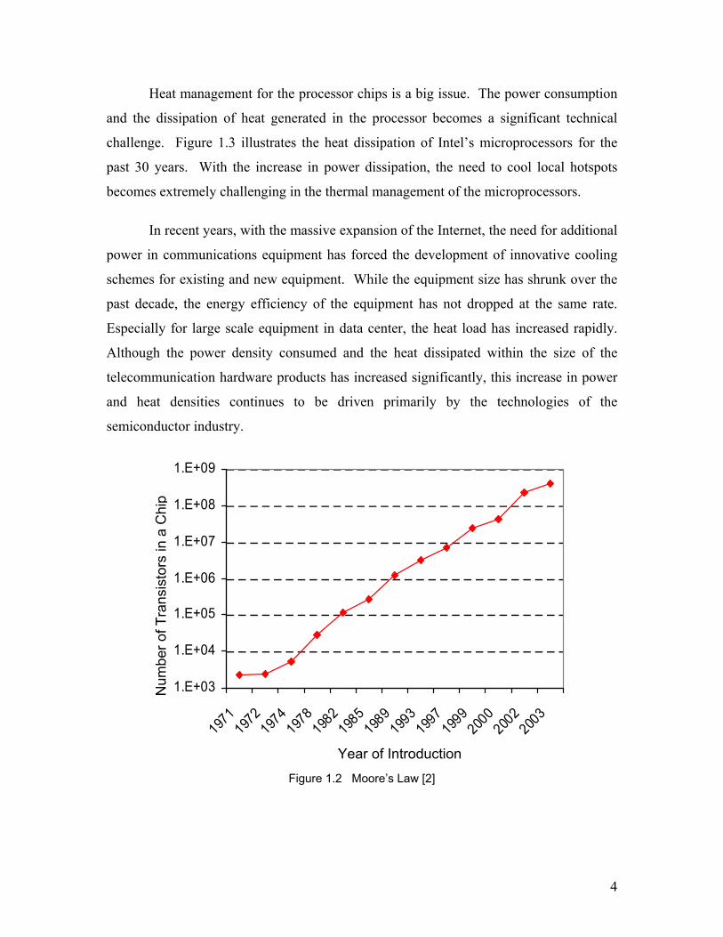
Pentium 4 microprocessor dissipating about 90 W of heat. Moore’s Law (Figure 1.2)
states that the transistor density on integrated circuits will double every 18 months. This
exponential growth and ever-shrinking transistor size would result in better performance
as well as the increase in the chip heat loss accordingly. As stated in the thermal design
guidelines for Pentium 4 [1], a typical aluminum extruded heat sink may not be adequate
to cool the entire range of thermal design power. To avoid potential failure, more
advanced cooling techniques are necessary to keep the processor within the operational
thermal specifications.
Figure 1.1 Functionality, Size, and Cost Driving the Development of Consumer Electronics
1980
Size
1990 2000 2010
Cost
Functionality
4
Heat management for the processor chips is a big issue. The power consumption
and the dissipation of heat generated in the processor becomes a significant technical
challenge. Figure 1.3 illustrates the heat dissipation of Intel’s microprocessors for the
past 30 years. With the increase in power dissipation, the need to cool local hotspots
becomes extremely challenging in the thermal management of the microprocessors.
In recent years, with the massive expansion of the Internet, the need for additional
power in communications equipment has forced the development of innovative cooling
schemes for existing and new equipment. While the equipment size has shrunk over the
past decade, the energy efficiency of the equipment has not dropped at the same rate.
Especially for large scale equipment in data center, the heat load has increased rapidly.
Although the power density consumed and the heat dissipated within the size of the
telecommunication hardware products has increased significantly, this increase in power
and heat densities continues to be driven primarily by the technologies of the
semiconductor industry.
Figure 1.2 Moore’s Law [2]
1.E+03
1.E+04
1.E+05
1.E+06
1.E+07
1.E+08
1.E+09
1971
1972
1974
1978
1982
1985
1989
1993
1997
1999
2000
2002
2003
Year of Introduction
Num
ber o
f Tra
nsis
tors
in a
Chi
p

5
Figure 1.3 Power Trend for Intel Microprocessor [3]
Uptime Institute [4] presented the heat density trends and projections for
information technology products as shown in Figure 1.4. The figure clearly shows the
rapidly increase in the heat load per product footprint for the products such as tape
storage systems, workstations, server and disk storage systems, as well as mainframe
communication equipments. With such high heat dissipation, the primary focus of the
thermal management for such equipment is to provide adequate air flow at a temperature
that meets the limited operating temperature of the components within the equipment.
1.2.2 Thermal Factors in Automotive and Motors Electronics
Power electronics is a major growth area within the automotive industry.
Automotive vehicles require sophisticated power management to support demands for
higher fuel efficiency, improved performance and increased electric loads. In particular,
electronic ignitions, power semiconductor voltage regulators, automatic motor controls,
and audio systems are some of the common applications. The power electronics
associated with these systems must be reliable over a wide temperature range. The
6
stability of these power automotive power systems depends on the reliability of the power
electronic converters as well as the power electronic components in the systems.
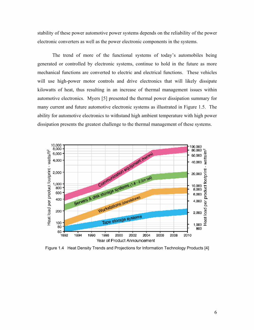
The trend of more of the functional systems of today’s automobiles being
generated or controlled by electronic systems, continue to hold in the future as more
mechanical functions are converted to electric and electrical functions. These vehicles
will use high-power motor controls and drive electronics that will likely dissipate
kilowatts of heat, thus resulting in an increase of thermal management issues within
automotive electronics. Myers [5] presented the thermal power dissipation summary for
many current and future automotive electronic systems as illustrated in Figure 1.5. The
ability for automotive electronics to withstand high ambient temperature with high power
dissipation presents the greatest challenge to the thermal management of these systems.
Figure 1.4 Heat Density Trends and Projections for Information Technology Products [4]

7
Figure 1.5 Thermal Power Dissipation Summary for Current and Future Automotive Electronic
Systems [5]
The worldwide market for electronic motor drives will grow from $12.5 billion in
2000 to $19.1 billion in 2005, according to a new market research study by Drives
Research Corporation [6]. The present trends toward energy efficiency, global
automation, precision control, and production flexibility predict a continued growth for
the electronic motor drives. Some applications for electronic motor drive include combat
vehicles, commercial transit such as hybrid electric and fuel cell vehicles, electric oil
field drilling equipment, machining systems, and conveyor applications.
Reliable motor drives are essential to provide high performance to the desired
functions as mentioned. However, almost all of the motor drives face harsh temperature,
humidity, and vibration condition during operations. One of the main approaches to high
reliability is to provide good thermal management to the motor drives. While both the
motor and the power electronics in the controls produce heat, the thermal management of
the motor drives can be improved with optimized design of mechanical components, heat
sink design, and components placement layout.

8
1.2.3 Thermal Factors in Lightning and Power Generation
Compact fluorescent lamps, high-intensity discharge (HID) lighting, high-
brightness LEDs, dimming and control systems for all types of lighting are some
examples of the applications of power electronics to lighting. Lamps are especially
sensitive to the supplied wattage and therefore they should be operated only at the
wattage they were designed for and with the type of current they were designed for. Both
under powering and over powering the bulbs can damage them and cause overheating. In
addition, at the end of the service life of high-intensity discharge lamps, the lamps may
overheat due to the rectifier effect. Igniters can also overheat in the event of a short
circuit in the associated ballast. One solution is to use a ballast with an integrated
temperature switch or a thermal protector to avoid damage due to overheating.
The blackout of August 14, 2003 affecting some 50 million people was a sharp
reminder of the essential nature of power failure. Flights were grounded, traffic lights
were out, subway and train systems were down, people were stuck in elevators, wireless
telecommunication network was down, and water could not be pumped. To prevent such
tragedy to happen again, all transmission lines, transformers, and electrical equipment
should be monitored to ensure the thermal limits are not exceeded. As you can imagine,
overheating of power electronics can cause severe failure in delivering the power to
individual home, business offices, and hinder our transit infrastructure, communication
network, as well as the water supply. As a result, the loss of electricity, lightning, and
telecommunications can cause serious inconvenience.
Driven by the recent surge in Internet usage coupled with the data center
construction craze, our nation's dependence on power is growing exponentially. There is
just not enough generating capacity to meet consumer demand. As a result, other power
generation sources emerge as an alternative energy to satisfy the nation’s demand. The
emergence of new developments in microturbine, fuel cell, solar, hydro and wind power
can help meet the nation’s energy needs.
Raw power output of alternative energy sources such as wind, solar, and fuel cell
needs to be converted into high quality alternating current required by the existing grid

9
infrastructure. To do so, advanced power electronics, particularly power inverters, are
intended to convert the raw power output of the alternative energy source as well as
manage the interconnection between the power supply and the grid. Therefore, reliable
power electronics are required for the integration of the alternative energy systems as part
of the power grid.
1.3 Current Packaging Technology for Power Electronics
A tremendous level of progress, technologically and demand-wise, of electronic
devices and systems has been achieved during the past decade. The progress surge has
come from the increased functionality and miniaturization of electronics at all levels.
The increased number of transistors and shrinking microprocessors size is a good effort
in increasing the functionality and miniaturization of the component size. Similarly, the
1U rack-mount system for servers is the example of high performance and space
minimization where all the components are fit into a 1.75” height chassis in this slim
design.
The increasing interest in high-density power electronics modules is driven by the
requirement to handle large numbers of power chips interconnections, high density heat
loss, and the desire to pack greater functionality into a compact volume. One of the
concepts to achieve these results is through the development of multi-chip modules. To
further increase the functionality of electronics components, thus the electronic systems,
today’s advanced packaging technologies offer integration of chips in a module to
achieve the desired increase functionality and minimal size.
The integration of multiple chips into a single multi-chip module package are
important to many applications where considerations of size, weight, and electrical
performance are required. Examples of commercially available multi-chip modules
include multi-chip module (MCM), ball grid array (BGA), and insulated gate bipolar
transistor (IGBT) intelligent power module (IPM) where the chips are attached onto a
substrate and interconnected using wire bonds. However, a consequence of this
integration is the increased necessity for thermal management.

10
The need to integrate more functionality into the module and higher switching
frequency has brought about a coupling of high power densities with tight circuit layout
that minimize delays in signal propagation. For every performance improvement in
electronic components and systems, there is a corresponding increase in the operating
heat generated by the devices. In today's advanced packaging technologies such as
system-on-a-chip, thermal management must be designed to handle maximum power
dissipation, power density, and hot spots at both the silicon and module levels.
What are the limitations of current practice? First of all, because of this
miniaturization and power increase, greater attention is being placed on thermal
management's role in the module's packaging design and interconnection. With the
current technology for multi-chips packages, almost all of the heat has to be extracted
through the solder layer that connects the chips to the substrate as illustrated in Figure 1.6
due to the high thermal resistances of the wire bonds. Secondly, the package is properly
encapsulated to protect the chips and the wire bonds from mechanical damage during the
handling. Most commonly used encapsulants are silicone and epoxy based. Although
silicone offers excellent moisture resistance and epoxy provides improved adhesion,
these materials are usually low in thermal conductivity. As a result, the heat generated
within the package can hardly be transferred through this layer of material to the ambient.
Figure 1.6 Heat Flow in Conventional Multi-chip Package
Substrate
Chip Chip
Solder
Wire Bond Encapsulant

11
In searching for solutions to overcome these limitations, new and emerging
technologies are introduced. The development of flip chip technology allows for
innovative interconnection rather than wire bonds. The interconnection between the die
and carrier in flip chip packaging is made through a conductive "bump" that is placed
directly on the die surface. The bumped die is then "flipped over" and placed face down,
with the bumps connecting to the carrier directly. However, the underfill in a flip chip
package makes rework much more difficult, which is a severe limitation to flip chip
technology.
1.4 Research Goals and Approach
The Center for Power Electronics Systems at Virginia Tech developed a novel
planar integration technology called Embedded Power. The Embedded Power
technology features metallization interconnections on co-planar power chips, which are
embedded in a flat ceramic carrier. The metallization is for the interconnection of
multiple power chips through metallurgical contact to aluminum pads on the power chips.
The power chips are then directly soldered onto a substrate. The substrate employed in
these prototypes is direct-bonded-copper (DBC) substrate. DBC substrate provides high
current interconnect, a good thermal path, and high voltage isolation. In addition, the
DBC substrate also provides a platform for soldering multiple power chips. In general,
an Embedded Power module consists of three layers as illustrated in Figure 1.7: the base
substrate, the embedded power (EP) stage, and the soldered component attached on the
top.
Figure 1.7 Structural Schematic of Embedded Power Module

12
While the electrical performance can be greatly improved with the proximity of
the interconnections, the closeness of the heat generating chips still causes hotspots
within the Embedded Power multi-chip module. Removal of generated heat from any
given chip within the module is essential to the effort of establishing long-term reliability
for a given device. To ensure the reliability of the Embedded Power multi-chip module,
this research addresses the thermal performance of the module.
Part of this research is to thoroughly analyze and evaluate multi-chip modules
packaged using Embedded Power technology such as integrated power electronics
modules (IPEMs), thus providing a strong background for a new and innovative cooling
strategy to be engineered. This research studies material and physical properties for the
Embedded Power modules. In addition, studies on integrated cooling strategies were
examined by implementing double-sided cooling and advanced cooling methods. The
final part of this research includes developing general thermal design guidelines for the
Embedded Power modules. These guidelines can help in guiding the future design of the
IPEMs as well as providing thermal management guidelines for the system designers.
In designing for thermal performance, the goal is to (i) allow the module to
operate at harsh environment such as high ambient temperature by reducing the overall
thermal resistance of the module as well as (ii) lengthen the life of the module. To
develop a reliable, cost-effective thermal solution, different cooling strategies for the
module should be considered. Therefore, modules can be cooled with active and passive
cooling solutions and can bring flexibility to the end users in different applications for
highest performance.
It is believed that the performance of multi-chip modules can be greatly improved
by using the introduced Embedded Power technology for integrating multiple chips into a
package. The electrical and thermal performance can be improved through integration
and miniaturization such as increased diversity and the number of miniature components
as shown in Figure 1.8. While the assembly of large numbers of heterogeneous
components can form a system capable of robust interaction with its environment, the
integration of components is limited by the heat transfer capability.

13
With the in-depth study on the thermal behavior and the heat transfer phenomena
for the Embedded Power modules, failure on the modules can be predicted and avoided
as necessary for better long-term reliability. Furthermore, essential thermal management
strategies can be developed and implemented to enable higher performance modules.
Specifically, the introduction of the thermal design guidelines can facilitate in future
design of the Embedded Power modules, thus reducing the design cycle time.
1.5 Dissertation Outline
This dissertation consists of seven chapters including necessary background,
motivation, and the objectives of the research effort in Chapter 1. Chapter 1 also
discusses limitations of the current practices as well as the impact of the research.
Chapter 2 reviews different packaging schemes for multi-chip modules as well as thermal
management for multi-chip modules. In addition, Chapter 2 discusses current practice on
the packaging of the multi-chip modules and its effect on the thermal management for the
multi-chip modules. Finally, a review in the area of thermal design guidelines is
presented in this chapter too.
Figure 1.8 Increased Performance with the Diversity and Number of Components through
Integration and Miniaturization
Perfo
rman
ce
Diversity and Number of Components

14
Chapter 3 presents detailed modeling of the Embedded Power module including
its structure and the thermal properties of the materials used for the Embedded Power
module. This chapter discusses the modeling approach as well as the validation of the
modeling tool with experimental results for obtaining an accurate and acceptable
numerical thermal model for future studies. With the validated thermal model in Chapter
3, the thermal models were then used for various studies addressed in Chapter 4. In depth
studies on the thermal behavior of the Embedded Power modules were conducted based
on various thermal design parameters such as material properties, sizes, and shapes. Both
numerical and experimental approaches were employed for these studies. In addition,
different integrated cooling strategies were also explored for improving the thermal
performance of the Embedded Power modules.
Chapter 5 discusses the results of the studies in Chapter 4. Based on the results
presented in Chapter 5, an in depth understanding on the thermal behavior of the
Embedded Power modules allows for enhanced thermal management for the Embedded
Power modules. Consequently, better thermal performance can be achieved. Chapter 6
presents the general thermal design guidelines for the Embedded Power modules. The
chapter also discusses the concepts for necessary concurrent design process incorporating
thermal design as well as various approaches in developing design guidelines.
Finally, Chapter 7 contains a summary of the conclusions of this research and the
contribution of this work towards new packaging technology for power electronics.

15
Chapter 2 Literature Review
The need for thermal management in electronics is inevitable in the foreseen future with
the anticipated significantly higher power dissipation than what is consumed in today’s
electronics. Increased demand for higher frequency and higher power dissipation has
increased the need for better thermal solutions. The purpose of electronics cooling is to
ensure that the electronic systems behave reliably under the most diverse environmental
and operational conditions.
2.1 Packaging Technologies for Multi-chip Modules
The present trend in electronic packaging is going towards high-density
packaging such as three-dimensional interconnects that allows stacking the chips and the
substrates in x-, y-, and z- direction. These packaging technologies enable the use of
different chip attachment technologies for the assembly of one or more chips into a single
module. This package technology promises tremendous size reduction while improving
the performance of the electronics. Multi-chip packages have become industry’s practice
to increase functionality in one high-density package. Different multi-chip packaging
technologies offer different advantages and thermal performances. In this section,
several commonly used packaging technologies for multi-chip modules are reviewed.
Extensive research in the past has focused greatly on the heat transfer in different
conventional packages such as ball grid array (BGA) packages, dual-in-line packages
(DIP), thin quad flat packages (TQFP), and pin grid array (PGA) packages. Figure 2.1
shows the package schematic for BGA packages, DIP packages, PQFP packages, and
PGA packages. Although the pin configurations for these packages are different, the
most commonly used interconnection techniques at the chip level are wire bond and
solder. Figure 2.2 shows the heat paths within the wire-bonded PGA packages. The
BGA package is a potential low-cost packaging solution to achieve miniaturization in
electronics. The BGA packages with wire-bond and flip chip die-to-substrate

16
interconnect are gradually replacing the traditional plastic quad flat packages.
Mulgaonker et al. [7] showed that thermal performance of the plastic ball grid array
(PBGA) compared well with ceramic pin grid array packages (CPGA), ceramic quad flat
pack (CQFP), and the ceramic BGA. The heat is transferred from the die through
thermal paths within the substrate and through the solder bumps into the printed wiring
board. The heat is then transferred out from the printed wired board to the ambient
through system level cooling as illustrated in Figure 2.3.
(a) BGA Package (b) DIP Package
(c) PQFP Package (d) PGA Package
Figure 2.1 Different Package Schematic

17
Figure 2.2 Schematic of Pin Grid Array Package and Its Heat Paths
Figure 2.3 Schematic of Ball Grid Array Package and Its Heat Paths
Mita et al. [8] proposed a high density package by mounting two chips on both
top and bottom sides of a small substrate by using tape automated bonding (TAB)
technology to form a chip on chip ball grid array (COCB) unit. Stiffeners are attached to
both sides of the COCB unit to maintain a flat outer surface for the unit. The individual
COCB unit can also be stacked to create a three dimensional module with heat spreaders
in between each COCB unit. The respective COCB unit is connected with electrical
Mold Chip Chip Chip
Solder Bumps
Substrate
Printed Circuit Board
Ambient
Compound
Ambient
Chip Chip Chip
Substrate
Ambient
Ambient
Printed Circuit Board
Pins
Plastic Cap
Wire Bonds

18
conductive adhesive or soldering and the heat spreaders are attached to the stiffeners by
adhesive. The COCB also showed a better lower package thermal resistance when
comparing to traditional plastic molded package where the molded resin has a
significantly high thermal resistance.
Yuan [9] compared the thermal performance and characteristics of flip chip and
wire bond ceramic multi-chip modules. He concluded that the flip chip packages offer
excellent thermal performance compared to the wire bond packages. He also found that
the significant parameters affecting the thermal performance of the wire bond packages
are the substrate thermal conductivity, substrate thickness, and the card thermal
conductivity. On the other hand, the significant parameters affecting the thermal
performance of the flip chip packages encapsulated with aluminum cap are the cap
material and the card thermal conductivity.
Kim [10] presented a folded stacked package for wireless and portable products
that allows dies to be placed side by side on a flexible substrate and folded to produce a
low-profile, compact package. The thermal analysis of a four-die folded staked package
showed that the junction to ambient of the package can be as high as 47 °C/W and about
96% of the heat is dissipated through the board. Furthermore, Balde [11] reviewed
several three dimensional assemblies of stacked chips and other thin packages. He
discussed the advantages and disadvantages of different commercial packages such as
leaded stacked packages, staked bare die using wire-bonding packages, staked bare die
using via interconnections packages, die staking with interposers packages, the
monolithic molded block approach, and frame wire-bonding assemblies. He then
introduced the folded flex assemblies as a new option in high density packaging
especially for memory modules and medical products. To achieve flexible
interconnections, Meyer et al. [12] used flexible foils to connect the ICs and surface-
mount devices.
Fan et al. [13] evaluated some of the key technologies that major semiconductor
manufacturers have adopted for discrete and multi-chip MOSFET module packaging for
power conversion applications. These included SO-8 based packages, chip scale, flip

19
chip, and ball grid array based packages as well as micro-lead frame based packages. In
the high thermal performance SO-8 based packages, copper straps and solder bumps are
the commonly used to replace wire-bonds. The larger contact area between the copper
strap and the chip can provide 10-20% better thermal performance as well as increasing
the amount of heat to be transported through the top of the chip. By replacing wire-bonds
with solder bumps at the backside of the chip to connect from the chips to the PCB in the
chip scale, flip chip, and ball grid array packages, the heat dissipation from the backside
of the chip to the PCB can be greatly improved. Therefore, the junction-to-PCB thermal
resistance can be greatly reduced. In the micro-lead frame based packages, device
interconnections are achieved with wire-bonds and the lead frame are soldered to the
bottom of the package.
To meet the capability of operating at high performance, current packaging
technologies for power electronics have moved towards high density interconnects. In
these packaging technologies, multiple power chips were integrated into a single compact
module by using different interconnect technologies such as wire bonding and thin film
overlay. Figure 2.4 shows the schematic of wire-bonding and flipped chip
interconnection. Ozmat [14] evaluated three different interconnect technologies: flipped
tape automated bond (FTAB) configuration, flipped chip package (FCP) configuration,
and high density interconnect (HDI) technology. He concluded that the HDI technology
offered a better alternative for high density multi-chip module applications than the
FTAB and FCP technologies because the HDI technology offers a direct heat path to the
chips.
(a) Wire-bonding (b) Flipped Chip Technology
Figure 2.4 Interconnection Schematic for (a) Wire-bonding and (b) Flipped Chip Technology
Chip
Substrate
Wire Bonds
Chip
Substrate
Solder Ball Underfill

20
Sienski et al. [15] presented a three-dimensional interconnect packaging concept
where integrated circuits (IC) chips were wire-bonded onto interconnect metal on the
diamond substrate. The top and bottom surfaces of the substrate were processed with
multi-layer high density interconnects such as copper and polyimide. The two sides were
electrically connected through metal-filled vias that penetrate the substrate. The top
surface of the high density interconnect was used to connect bond pads. In their study,
heat removal from the package was achieved through phase change spray cooling.
In 1997, Ozmat et al. [16] presented a new packaging approach called Harris Thin
Pack (HTP) to package high performance power devices. The HTP package contained a
combination of multiple discrete power devices and diodes. The key element of HTP
package was a dielectric lid that contains patterns of metallization on the top and the
bottom surfaces. Finite element analysis and experiments were performed to evaluate the
thermal performance of the package. In this package, high performance heat exchangers
were incorporated into the package to achieve maximum thermal performance.
In addition, Fisher et al. [17] presented the thin film power overlay technology
(POL) for power modules where layers of dielectric and patterned copper on top of a
substrate to form a dense interconnect structure. Chips are mounted on top of the
interconnection by various methods including wire bonds and solder bumps. This
technology enables the chips to be soldered directly to a DBC substrate which acts as the
bottom interconnect layer for the chips. Furthermore, POL technology eliminates bond
wires. The planarity of the package structure enables double-sided cooling where heat
can be removed from the top and bottom sides of the module.
The need for smaller and less expensive power converters for consumer
electronics and military power systems has pushed for new packaging technologies. The
standardization of power electronics modules can replace complex power electronic
circuits and simplify the development and design of large electric power systems.
To increase the degree of integration for power modules packages, Stockmeier et al. [18]

21
presented intelligent power electronics modules such as SKiiP1. The intelligent power
electronics modules not only integrated power devices but also included a gate drive unit,
as well as temperature and current sensors. Other available commercial integrated power
modules include products from Fuji [19], Eupec [20], and Toshiba [21].
Lostetter et al. [22] presented the concept of standardized integrated power
modules (IPM) by extending multi-chip module laminate (MCM-L) concepts to power
electronics packaging. The foundation of the module is a piece of DBC where the bare
dies are soldered to the DBC. A nonconductive ceramic or polymer spacer with cavities
is used to embed the bare dies, and the bare dies are wire-bonded on the top surface of the
bare dies. The entire structure is soldered to a copper or metal matrix composite (MMC)
heat spreader for proper thermal management.
Similar to the structure of the POL and IPM, Liang et al. [23-25] presented
embedded power technology for integrated power electronics modules (IPEM). The
embedded power technology is a deposited metallization based integration technology.
The embedded power packaged module consists of the embedded power stage, the
electronics circuitry such as the gate drive and the control components, and the base
substrate. The concept of the embedded power technology for integrated modules is
shown in Figure 2.5. The power chips are embedded in the openings of a ceramic with
adhesive dielectric surrounding the chips. An interlayer dielectric is applied on top of the
chips and the ceramic with via holes for interconnection to the aluminum pads on the
chips. Patterned copper metallization layers are deposited onto the dielectric layer and
through the via holes to form interconnections with the aluminum pads on the chips.
Different three-dimensional modules can be packaged using the embedded power
technology by using different interconnect pattern depending on the desired functions and
applications of the three-dimensional packages.
1 SKiiP is a registered trademark of Semikron Electronic

22
Figure 2.5 Concept of Embedded Power Technology
Most of these multi-chip packaging technologies are used by industry nowadays.
Therefore, many studies have been conducted to understand the advantages and
disadvantages of these packaging technologies from the view points of electrical
performance, thermal performance, reliability, process of integration, and cost. Ginsberg
et al. [26] summarized some general considerations for different packaging technologies
for multi-chip modules. While other common packaging technologies such as BGA
packaging technologies and wire-bonding interconnection are well-studied, there is still
much work to be done on embedded power technology. Therefore, an in-depth
understanding of the advantages and disadvantages of using embedded power technology
and its consequent advantages from the IPEM can greatly promote its practical use in
industry.
2.2 Component Level Cooling Technologies
The need to miniaturize and improve the performance of the conventional
electronics has pushed the development of multi-chip module in which two or more bare
chips are interconnected on a common substrate. The ability to integrate more
functionality into a smaller area and the ability to operate at higher frequencies in multi-
chip modules have also increased the challenge in the thermal management of the
package due to the higher power dissipation. A diverse set of constraints, among them
Ceramic
Power Chip Power Chip
Substrate
Trace
Solder
Dielectric Metallization
Surface Mount Components
Trace

23
cooling performance, may ultimately limit the overall performance at which a technology
can reliably be operated.
Thermal management design has a significant impact on package form factor and
shape. Heat generated inside the package must be transferred to the surface of the
package and dissipated from the package to ambient by any available cooling strategies.
In summary, the thermal management process can be categorized into three major phases
as illustrated in Figure 2.6:
I. Heat transfer within the component package,
II. Heat transfer from the package to a heat spreader or heat sink, and
III. Heat transfer from the heat spreader or heat sink to the ambient environment.
The package type defines the internal heat transfer processes in the first phases
and the system level thermal engineer does not usually have control of it. The goal of the
packaging engineer in the second and third phases is to design a reliable, efficient thermal
connection from the package surface to the heat spreader or heat sink and to the ambient
environment. To achieve this goal, a package level thermal engineer is required to have a
thorough understanding of heat transfer fundamentals and the knowledge of available
interface and good thermal conductivity materials.
Figure 2.6 Three Major Phases of Heat Transfer at Component Level
Chip
Substrate
Heat Spreader
Ambient
Ambient
Heat Sink
Phase II
Phase I
Phase III

24
2.2.1 General Thermal Management Overview
Bergles [27] extensively summarized the use of cooling technologies for
electrical, electronic, and microelectronics for the past 50 years. Some of these
technologies included conduction cooling, air cooling, and liquid cooling. In conduction
cooling, heat is transferred by conduction to the fins which are cooled by convection and
radiation. In other cases of conduction cooling, heat is conducted by one end of the heat
pipe to the other end where the other end is cooled by convection or radiation. Natural
air convection and forced air convection are categorized in the air cooling technique. In
liquid cooling, liquid can be forced to flow through a channel with mounted devices and
the liquid is cooled in an air or liquid-cooled heat exchanger. The devices can also be
submerged in a boiling liquid where heat is rejected to an air or water-cooled condenser.
In addition, devices can also be mounted in an enclosure filled with dielectric fluid and
cooled by air-cooled or water-cooled heat exchanger.
Price [28] reviewed several thermal management solutions for military
electronics systems, including direct and indirect air cooling of printed wiring boards,
liquid-cooled flow-through power supply, liquid-cooled and two-phase cold plates,
expendable liquid systems, implementation of phase change materials, implementation of
thermoelectric coolers, and stirling cycle mechanical cryogenic cooler. These cooling
methods are implemented in the design of modular microwave integrated circuits devices.
These devices are used in missile electronics, NASA communication arrays, the Discover
II Satellite Communications Systems, military infrared detector arrays, target acquisition
systems, ground-based night vision systems, and airborne electro-optics forward looking
infrared (FLIR) systems.
In addition, Azar [29] presented several active cooling options as well as their
advantages and disadvantages. These options included fan and heat sinks or heat pipe
combinations, air flow management and enhancement, hybrid cooling, thermoelectric,
thermosyphon, closed loop liquid cooling, direct immersion, refrigeration, and
cryogenics. While these advanced cooling technologies can greatly improve the thermal
performance of the electronics, the common constraints of these technologies are the cost
of packaging and the reliability of the system.

25
2.2.2 Thermal Management for Multi-chip Modules
The introduction of multi-chip modules has brought new challenges to the thermal
management techniques in electronics. The high density integration in the multi-chip
modules results in higher heat flux densities at the component-level packaging
technologies. In addition, the wide variety of materials used in the modules and the
varying coefficients of thermal expansions (CTE) involved in the multi-chip modules
present more difficult problems in thermal management. While the purpose of the
thermal management is to ensure that the circuit components are maintained within their
functional temperature limits, the generated heat within the modules is usually dissipated
through conduction, convection, and radiation.
Heat generated within the multi-chip modules is usually transported by
conduction to the external surfaces of the package. From there, the heat is then
transferred to external heat sinks by conduction or convection. Very often the heat is
removed through the back side of the components because the top side of the components
is encapsulated for safety and protection purposes. Thus, the thermal resistance from the
chip to the top surface of the package is significant higher than the thermal resistance
from the chip to the back side of the package.
While most of the heat is conducted through the back side of the chip through the
solder interconnects to the substrate, Patel [30] presented a backside cooling solution for
high power flip chip multi-chip modules. The design used a high thermal conductivity
(2.8 W/m-K) thermal compound with an innovative referencing scheme for interfacing
the chips to the heat sink. The heat sink was used for convective heat flow.
Lee [31] presented several thermal enhancing techniques for flip chip plastic ball
grid array (BGA) packages. He studied 26 different thermal enhancing methods. These
included the effect of attaching a copper heat spreader with different thicknesses to the
back side of the die, effective area covered by the interface material, attachment of
aluminum lid, and the attachment of heat sink. He concluded that attaching a copper heat
spreader on the back side of the die can significantly increase the heat flow projection.
Furthermore, using high thermal conductivity molding compound can also reduce the

26
junction-to-ambient thermal resistance. On the other hand, Liang et al. [32] presented
multi-chip modules encapsulated with crimped metal cap which provides lower thermal
resistance on the top side of the module compared to molding compound.
To improve the heat transfer from the heat source to an external surface of a
package, Pittler et al. [33], Chu et al.[34], Blodgett et al.[35], and Oktay et al. [36]
presented the development of the thermal conduction module (TCM). The TCM has a
helium-based module cap which provides a thermal conduction path from the back of
each chip, via one contacting piston per chip, to the cap. The cap is in contact with a
water-cooled cold plate. The chip temperatures are established by the external and
internal thermal resistances to heat flow from the chip to the cap, to the cold plate, and to
the board on which the modules are held by special connectors. They concluded that the
power dissipation limits can be extended by over 50% with the TCM combines the
advantages of conduction cooling used at the chip and module levels with that of the
forced convection liquid cooling at the system level.
Mudawar [37] reviewed several different high heat flux thermal management
schemes. These included avionic air cooling, micro-channel and mini-channel cooling,
jet impingement cooling, and spay cooling. In addition, he also listed the saturated
thermophysical properties of different liquid coolant used in liquid cooling. These
commonly used coolants include FC-72, FC-87, PF-5052, and water. He concluded that
phase change plays a key role in attaining attractive cooling performances although phase
change systems are generally more complicated to implement. Lee et al. [38]
demonstrated the capability of using a liquid-filled cooling environment to enhance the
thermal performance of a multi-chip module package. The package was externally
cooled by either free-air or forced-air. High thermal properties of dielectric liquids
showed promising 2-4 times improvement in the thermal performance compared to air.
In addition, Chen et al. [39] investigated the thermal performance of a stacked
multi-chip module using direct liquid cooling with single phase FC-72 as the working
fluid. Experimental and numerical studies were conducted. They concluded that using
liquid cooling can further increase the package power loss. Furthermore, Shaw et al. [40]

27
implemented direct low-pressure water spray-cooling on the surface of the diodes within
a variable-speed motor drive. The surfaces of the exposed devices and interconnects
were coated with 25 micron of Parylene as a dielectric layer.
The use of a thermoelectric cooler for spot cooling had also shown to be an
effective way to improve the thermal performance of electronics equipments back in
1961 [41]. They have been used for over three decades for electronics cooling. Fleurial
et al. [42] presented novel thermal management approach that used thermoelectric cooler
located under each of the power devices to cool only the key high power devices.
Simons et al. [43] reviewed the application of thermoelectric cooling to the cooling of
electronic equipment. They concluded that the heat loss from multi-chip modules are
simply too high for current thermoelectric modules to provide enhancement effectively.
In other application, Solbrekken et al. [44] proposed to convert the waste heat from the
CPU to generate electricity using a thermoelectric module drive the cooling fan.
Advanced materials are commonly used as passive thermal management
strategies for electronics. The continuing increase in packaging density and power levels
has resulted in a need for high thermal conductivity materials. In addition to the thermal
properties, the matching of the coefficient of thermal expansion (CTE) of adjacent
materials in the package is also crucial in minimizing thermal stress for potential failure.
Zweben [45] presented an overview of composites used in and thermal management and
evaluated their thermal conductivities and CTE values. These composites included
silicon carbide particle-reinforced aluminum, carbon fiber-reinforced copper, carbon
fiber-reinforced aluminum, diamond particle-reinforced copper, and beryllia particle-
reinforced beryllium.
Jha [46] introduced a new thermal management material named CUVAR.
CUVAR is an extruded composite of copper and Invar powder and can be used as heat
sinks or substrates for direct bonding the silicon devices. Invar restrains thermal
expansion and copper provides high thermal conductivity. However, exposure of
CUVAR to temperature higher than 700°C could cause degradation in its physical
properties. Davidson et al. [47] presented a copper-diamond composite material with

28
higher thermal conductivity and closer CTE with silicon and gallium arsenide as substrate
material for multi-chip module.
2.3 Tools for Thermal Prediction and Thermal Test Method
Temperature is an important parameter that must be controlled in electronics to
ensure long term reliability of the electronics. However, the heat transport in electronic
systems is, in most cases, not immediately well understood. Therefore, different
techniques are employed to improve the understanding of the heat transfer in electronics
systems. Commonly used techniques include analytical and computational approaches as
well as experimentation.
Accurately predicting the operating temperature of critical electronic parts often
presets an overwhelming challenge. Ellison [48] presented analytical and computational
approaches of solving heat transfer problems in electronic equipment. He confined the
numerical approach to conduction, radiation, and convection by natural and forced
airflow and presented two computer programs named Thermal Analyzer for Multilayer
Structures (TAMS) and TNETFA. Eid [49] outlined the methodology of performing
multi-dimensional thermal modeling using a spreadsheet.
Many commercial computational fluid dynamics and heat transfer tools for
thermal design of electronics components and equipment are available in the market.
Mak et al. [50] introduced an approximate analysis method incorporated in ANSYS for
thermal finite element analysis of a surface mount plastic package mounted on a printed
circuit board. This approximate numerical technique employs a point matching method
at the board mounting locations where the temperature and heat flow continuity
requirements are enforced. In addition, Zahn [51] benchmarked the capabilities of two
CFD software tools, IcePak and Flotherm, to predict flow fields and heat transfer in a
package level, laminar flow, and natural convection environment.
Although numerical modeling are widely used for the thermal analysis of
electronics components and systems, Joshi et al. [52] concluded that the key challenges in
thermal modeling include the solution methodology, the uncertainty of input parameters,
and the measurement uncertainties in providing meaningful validation for computational

29
simulations. To identify the capabilities of current algorithms used for CFD modeling,
Eveloy et al. [53] reviewed the potential shortcomings of the fluid flow modeling
currently employed for printed circuit board thermal analysis especially the turbulence
models in the CFD codes. Therefore, computational approach can not always correctly
describe the heat transfer in electronic equipment especially when convection and fluid
flow is involved. For the same reason, experimentation is needed to benchmark the
computational program as well as provide insight to the thermal behavior of the
electronic equipment.
Experiments are conducted at all levels of the design cycle to ensure system
integrity and adherence to design specifications. Common goals for performing
experimentation include component characterization, validation of numerical models, and
operational integrity. Experimental measurement can provide reliable information for
knowing the junction temperature and consequently the thermal behavior of the
electronic package. Hence, it is necessary to generate important and accurate data in
order to achieve the design objectives.
Azar [54] outlined important steps to successful measurement in electronic
enclosures. He also reviewed tools necessary for a successful analysis and their
limitations and domain of application identified. Kromann [55] used experimentation to
perform thermal characterization of an alumina-tungsten multilayer multichip module.
He showed that the experimental measurement variability was small. Other researchers
have also conducted experimentation for the purpose of validation [56-58]. To
understand these experimental methods, the Joint Electron Device Engineering Council
(JEDEC), under the Electronic Industries Association (EIA), is creating thermal
measurement standards for integrated circuit packages by which the performance of
different packages housing similar devices, or different devices in similar packages can
be compared [59].
Uncertainty analysis can identify the uncertainties in measurements and evaluate
their effect on the accuracy of the results. Moffat [60] presented a procedure for

30
estimating the uncertainties in the experimental results as well as outlined possible
sources of errors.
2.4 Thermal Design Guidelines for Multi-chip Modules
The thermal design guidelines for single-chip electronics are well established.
The standard guidelines for determining the thermal resistance of a single chip package
are well documented by JEDEC [59]. On the other hand, there is no standardized method
available to determine the thermal resistance for multi-chip packages. A common
parameter used for the comparison of various single-chip thermal designs is the junction-
to-ambient thermal resistance, Rja. However, this single parameter cannot effectively
describe three-dimensional heat flow in multi-chip modules. Researchers have presented
methods to determine the equivalent thermal resistance for each die in a multi-chip
module [61, 62].
Liang et al. [63] addressed the thermal issues affecting the thermal performance
of the multi-chip modules. These included the spreading resistance, the non-symmetrical
heating in the module, the substrate materials, and the thermal vias. In addition to
component level thermal design guidelines, Lall et al. [64] presented thermal design
guidelines for predicting the maximum temperature of a heating component on a
conducting board with uniform surface conductance on the top and bottom surface.
Although design guidelines are not well-established for the thermal design of
electronics especially multi-chip modules, the design guidelines for very large scale
integration (VLSI) design are well developed. For example, Watanabe et al. [65]
presented design guidelines for HfSiON gate dielectrics for 65 nm CMOS generation. In
addition, geometry constraints such as minimum allowable values for certain widths,
separations, extensions, and overlaps of geometrical objects patterned in the various
levels of a system are widely used in the VLSI design [66]. VLSI circuit layout design-
rule checking to reduce errors in the VLSI designs is also well studied [67]-[69].

31
2.5 Summary
The evolution of electronic packaging technology has posed greater challenges for
the thermal design. Miniaturization with increased integration in functionality and
components, as well as higher heat loss from the semiconductor continues to be a major
concern. Traditional and novel cooling strategies have been studied over the past few
decades for different applications, both in consumer electronics and military electronics.
Various tools and methodology are used to predict the thermal performance of the
semiconductor in electronics as well as the electronics equipment. In summary, increase
in the power dissipation in electronics will continue to drive the need for novel thermal
management strategies. The importance of thermal management to the ultimate success
of future electronics will not diminish.
Although Embedded Power technology is a rather new technology, it resembles
flip-chip packages in taking the advantage of the area under the package for the solder
interconnections. Therefore, we can presume that the main heat path within the
Embedded Power module is from the chip through the solder layer to the substrate as
illustrated in Figure 2.4 (b). In addition, the metallization bonding technique in the
Embedded Power technology resembles the power overlay technology where layers of
dielectric and patterned copper on top of a substrate to form a dense interconnect
structure. Thus, we believe that the planarity of the metallization layer can be used for
double-sided cooling as suggested by the literature in [17].

32
Chapter 3 Thermal Modeling of IPEMs
Thermal modeling is important at the electronics design stage where different
developments and explorations can be performed without expensive and time consuming
modifications. It also allows engineers to understand the thermal behavior of the
electronics components and their interrelationship between the electronics components as
well as the thermal dynamics of the system. The implementation of thermal modeling in
the design process can ensure good thermal management for the electronics components
in the electronics systems.
Traditional power electronic modules are based on standard industry
semiconductor package configurations. Heat is conducted from the chip through the wire
bonds and solder to the bottom of the package base, and then through an interface
material into a heat spreader and heat sink for either air-cooled or water-cooled
applications. Heat is also conducted through some thick compound material or electrical
insulated layer to the top of the package. However, almost all of the heat is conducted
through the package base rather than to the top of the package due to the higher thermal
resistance of the compound material or the insulation layer.
On the other hand, the heat transfer in planar multi-layer structures is usually
more complicated than in the traditional power electronics structures since it is three-
dimensional with spatially distributed thermal resistances and capacitances. Therefore,
good analysis tools are required to analyze the planar multi-layer structured power
electronics modules and to predict the temperature distribution of these structures. This
chapter presents the details of the finite element thermal modeling of IPEMs and the
validation of the numerical models against the experimental results.

33
3.1 IPEM Structure and Packaging Scheme
In power electronics, it is believed that the next level of improvement can be
achieved by integrating discrete components into a single multi-chip module. To
understand the thermal behavior of planar multi-chip packaged power electronics
modules, two active integrated power electronics modules, direct current to direct current
(DC/DC) and power factor correction (PFC) IPEMs, were studied in this research.
Active IPEMs integrated typical active discrete components such as MOSFETs and
diodes for front-end DC/DC converters into a high density package.
The IPEMs described in this research were designed for a 1 kW DC/DC converter
for distributing power system (DPS) applications with 400 V input bus voltage and 5 A
root-mean-square (RMS) current operating at 200 kHz switching frequency. The IPEMs
were packaged using Embedded Power technology. This technology features the
building-up of interconnects on co-planar power chips that were embedded in a ceramic
frame. In other words, the Embedded Power technology replaces the wire bonds with
deposited copper metallization layers for electrical connections. Through this advanced
interconnect technology, the electrical and mechanical performances of the modules were
improved by the elimination of the resistance, noise, and fatigue failure of the wire
bonds. Figure 3.1 shows the conceptual structure of Embedded Power module presented
by Liang [23].
Figure 3.1 Conceptual Structure of Embedded Power Module
Substrate Ceramic
Dielectric MetallizationComponents
Silicon Die
Silicon Die
Solder Solder

34
The DC/DC IPEM consists of two MOSFET bare chips soldered to a direct-
bonded-copper (DBC) substrate. While the DBC substrate consists of three layers with a
ceramic substrate sandwiched between two layers of copper, the DBC substrate provides
a good current interconnection, high electrical isolation, and a good thermal path for the
MOSFET chips. The top copper layer of the DBC substrate was etched to desired
patterns as interconnect platform for the chips. To integrate multiple chips into one
compact module, a ceramic carrier with openings was used to frame the MOSFET chips.
The silicone gel, with a thermal conductivity of 0.2 W/m-K, filled the gap formed
between the DBC ceramic and the ceramic carrier due to the etched copper traces. The
epoxy, with a thermal conductivity of 1.4 W/m-K, filled the gap between the MOSFET
chips and the ceramic carrier to secure the position of the MOSFET chips.
An inter-layer dielectric using polyimide was coated onto the top and bottom of
the ceramic carrier using polymer screen-printing method. The flat surface of the
ceramic carrier also provides a platform to deposit copper metallization layer on top of
the MOSFET chips for electrical interconnection. The patterned metallization with via
holes were designed based on the aluminum pad pattern of the chips. Finally, a hybrid
gate driver was assembled to the module for controlling the circuitry of the module. The
DC/DC IPEM has a footprint of 28.5 mm x 27.3 mm. Table 3.1 lists the physical
dimensions and the material characteristics of the components in the DC/DC IPEM.
Similarly, the PFC IPEM was also packaged using Embedded Power technology.
Instead of MOSFET chips, there are two CoolMOS1™ chips and two silicon carbide
(SiC) diodes in the PFC IPEM. Other components such as the embedded capacitors and
the embedded current sensor are also part of the PFC IPEM. In addition, a commercial
gate driver was also attached to the PFC IPEM. The footprint of the PFC IPEM is 34.2
mm x 29.7 mm. For safety purposes, the top surface of the active IPEMs was
encapsulated with silicone gel for electrical isolation. The physical dimensions and the
material characteristics of the components in PFC IPEM are listed in Table 3.2. Both
DC/DC and PFC IPEMs are shown in Figure 3.3.
1 CoolMOS is a trademark of Infineon Technologies
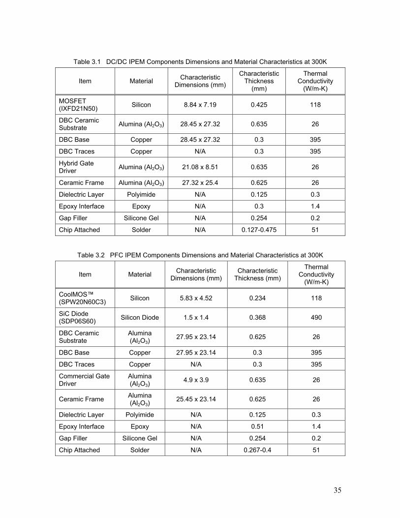
35
Table 3.1 DC/DC IPEM Components Dimensions and Material Characteristics at 300K
Item Material Characteristic Dimensions (mm)
Characteristic Thickness
(mm)
Thermal Conductivity
(W/m-K)
MOSFET (IXFD21N50) Silicon 8.84 x 7.19 0.425 118
DBC Ceramic Substrate Alumina (Al2O3) 28.45 x 27.32 0.635 26
DBC Base Copper 28.45 x 27.32 0.3 395
DBC Traces Copper N/A 0.3 395
Hybrid Gate Driver Alumina (Al2O3) 21.08 x 8.51 0.635 26
Ceramic Frame Alumina (Al2O3) 27.32 x 25.4 0.625 26
Dielectric Layer Polyimide N/A 0.125 0.3
Epoxy Interface Epoxy N/A 0.3 1.4
Gap Filler Silicone Gel N/A 0.254 0.2
Chip Attached Solder N/A 0.127-0.475 51
Table 3.2 PFC IPEM Components Dimensions and Material Characteristics at 300K
Item Material Characteristic Dimensions (mm)
Characteristic Thickness (mm)
Thermal Conductivity
(W/m-K)
CoolMOS™ (SPW20N60C3) Silicon 5.83 x 4.52 0.234 118
SiC Diode (SDP06S60) Silicon Diode 1.5 x 1.4 0.368 490
DBC Ceramic Substrate
Alumina (Al2O3)
27.95 x 23.14 0.625 26
DBC Base Copper 27.95 x 23.14 0.3 395
DBC Traces Copper N/A 0.3 395
Commercial Gate Driver
Alumina (Al2O3)
4.9 x 3.9 0.635 26
Ceramic Frame Alumina (Al2O3)
25.45 x 23.14 0.625 26
Dielectric Layer Polyimide N/A 0.125 0.3
Epoxy Interface Epoxy N/A 0.51 1.4
Gap Filler Silicone Gel N/A 0.254 0.2
Chip Attached Solder N/A 0.267-0.4 51

36
(a) DC/DC IPEM (b) PFC IPEM
Figure 3.2 Pictures of DC/DC and PFC IPEM
3.2 Basic Finite Element Thermal Modeling of IPEM
The finite element models were created using commercial software, I-DEAS2™.
I-DEAS™ provides a solid modeler to model solid geometry and electro-system cooling
(ESC) solver for thermal simulations. ESC allows conjugate heat transfer analysis with
comprehensive 3D computational fluid dynamics (CFD) solutions. In addition, ESC
combines finite element modeling (FEM) based analysis with control volume formulation
to achieve accurate solutions. The fluid flow and thermal model are solved iteratively.
More information on the capabilities of ESC can be found in [70].
The ESC solver allows for conductive, convective, and/or radiative analyses. In
this study, radiation was assumed negligible, and both conductive and convective modes
were used. Conduction is a process of heat transfer from a solid-solid interface due to the
atomic or molecular activity. A general conduction rate equation is known as Fourier’s
Law and can be expressed as follows:
)zTk
yTj
xTi(k"q
∂∂
+∂∂
+∂∂
⋅−= , (3.1)
where q” is the heat flux, k is the thermal conductivity, and T is the temperature. It can
be observed from Eq. 3.1 that the heat flux is a directional quantity. 2 I-DEAS is a trademark of UGS Corp.

37
The process of heat transfer from a solid-fluid interface due to fluid motion is
known as convection. The overall effect of convection heat transfer is known as
Newton’s law of cooling and can be expressed as follows:
)TT(AhQ aw−⋅⋅= , (3.2)
where Q is the quantity of the heat convected, h is the heat transfer coefficient in W/m2-K
, A is the convecting surface area, Tw is the temperature of the convecting wall, and Ta is
the ambient fluid temperature.
Any component level thermal analyses must consider the details of the power
electronics package. Understanding the physical structure of the package is the first step
in the analyses process. The basic numerical models of the active DC/DC and PFC IPEM
are shown in Figure 3.3. The finite element models included 2D linear triangle shell
elements and 3D linear tetrahedron solid elements. To improve the accuracy of the
simulation results, all available details were included in the models. Due to the thin layer
of the interface materials, interface conditions within the modules were specified as
equivalent thermal resistances. The details of obtaining these equivalent thermal
resistances at the interfaces can be found in Appendix A.
Unknown interface conditions were modeled as estimated values based on
engineering judgment. These interfaces included solder layers, epoxy layers, and
polyimide layers. The calculated equivalent thermal resistance values for these interfaces
are presented in Appendix A. Figure 3.3 (b) shows the locations of these interfaces
within the PFC IPEM. Note that the interfaces in the DC/DC IPEM are similar to the
PFC IPEM shown in Figure 3.3 (b). The hybrid gate driver in the DC/DC IPEM was
modeled as a homogenous block with its thermal conductivity equivalent to alumina. On
the other hand, the commercial gate driver in the PFC IPEM was not considered in the
thermal model since it has negligible heat load. Overall, the hybrid gate driver in DC/DC
IPEM, the commercial gate driver, the embedded capacitors, and the current sensor in the
PFC IPEM add negligibly to the heat load in the IPEMs, and were therefore not
considered further.

38
Heat generation in the power chips was assumed to be uniform on the top surface
of the chips. The main heat paths within the active IPEMs were from the heat sources to
the copper traces to the DBC ceramic, and from the DBC ceramic to the DBC copper
base. From there, the heat dissipated through conduction from the DBC copper base to
the copper heat spreader and to the heat sink. Heat was then transferred to ambient air
through convection. Other heat paths included from the heat source to the top copper
metallization layer connected to the DBC traces. Although there was possible heat path
from the top copper metallization layer to the top encapsulated gel and to the ambient air,
the encapsulated gel has rather high thermal resistance that prevented top side cooling.
Therefore, the top surface of the active IPEMs was modeled as adiabatic surface in the
finite element models.
The power dissipations of the power chips during actual operation of the DC/DC
converter were unavailable. Therefore, calculated values based on operating conditions
were used in most of the cases studied in this research. The calculated values are listed in
Table 3.3. However, specific power dissipations for each investigated case will be
specified in the individual case study discussed in Chapter 4.

39
(a) DC/DC IPEM
(b) PFC IPEM
Figure 3.3 Solid Models of (a) DC/DC IPEM and (b) PFC IPEM with Location of Interfaces Modeled as Equivalent Thermal Resistances
DBC
Embedded Capacitors
CoolMOS™ 2CoolMOS™ 1
SiC Diode 1SiC Diode 2
Gel
Ceramic Carrier
Embedded Cap Metallization
Power Stage Metallization
Top Polyimide*
Bottom Polyimide* Solder*
Epoxy*
* Interface Modeled as Equivalent Resistances
DBC Copper
DBC Ceramic
Copper Traces
MOSFET 1MOSFET 2
Ceramic Carrier
Hybrid GateDriver Copper
Metallization
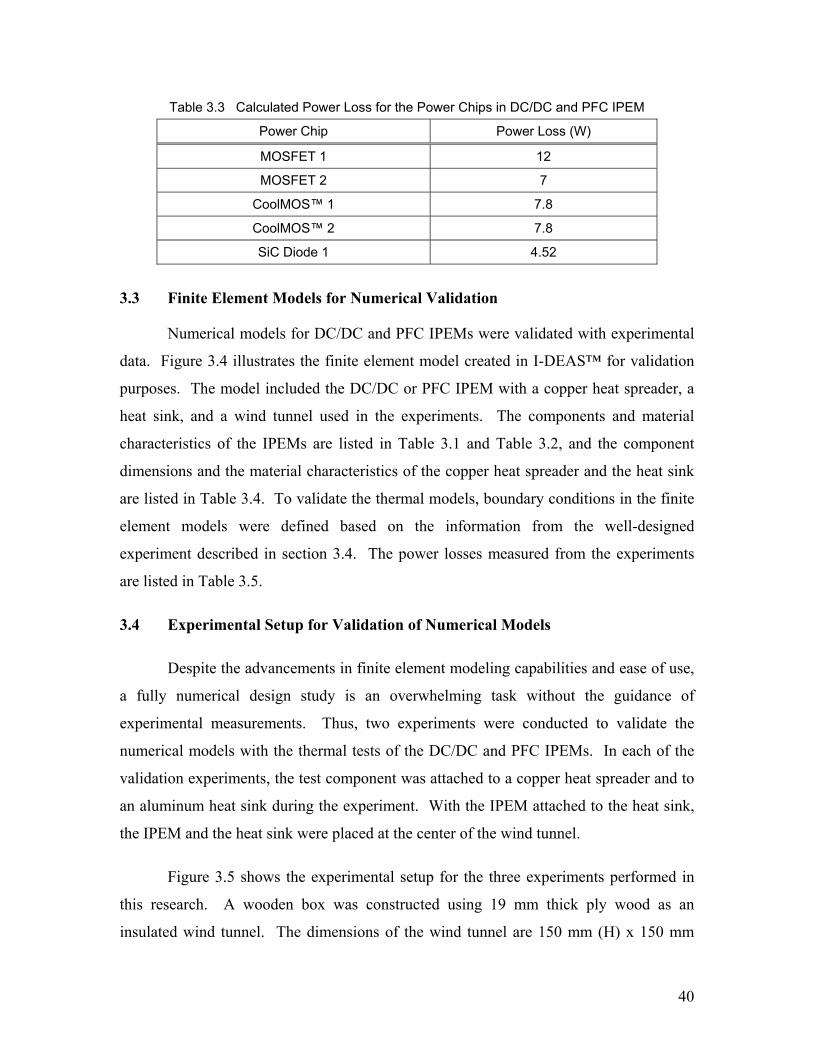
40
Table 3.3 Calculated Power Loss for the Power Chips in DC/DC and PFC IPEM
Power Chip Power Loss (W)
MOSFET 1 12
MOSFET 2 7
CoolMOS™ 1 7.8
CoolMOS™ 2 7.8
SiC Diode 1 4.52
3.3 Finite Element Models for Numerical Validation
Numerical models for DC/DC and PFC IPEMs were validated with experimental
data. Figure 3.4 illustrates the finite element model created in I-DEAS™ for validation
purposes. The model included the DC/DC or PFC IPEM with a copper heat spreader, a
heat sink, and a wind tunnel used in the experiments. The components and material
characteristics of the IPEMs are listed in Table 3.1 and Table 3.2, and the component
dimensions and the material characteristics of the copper heat spreader and the heat sink
are listed in Table 3.4. To validate the thermal models, boundary conditions in the finite
element models were defined based on the information from the well-designed
experiment described in section 3.4. The power losses measured from the experiments
are listed in Table 3.5.
3.4 Experimental Setup for Validation of Numerical Models
Despite the advancements in finite element modeling capabilities and ease of use,
a fully numerical design study is an overwhelming task without the guidance of
experimental measurements. Thus, two experiments were conducted to validate the
numerical models with the thermal tests of the DC/DC and PFC IPEMs. In each of the
validation experiments, the test component was attached to a copper heat spreader and to
an aluminum heat sink during the experiment. With the IPEM attached to the heat sink,
the IPEM and the heat sink were placed at the center of the wind tunnel.
Figure 3.5 shows the experimental setup for the three experiments performed in
this research. A wooden box was constructed using 19 mm thick ply wood as an
insulated wind tunnel. The dimensions of the wind tunnel are 150 mm (H) x 150 mm

41
(W) x 400 mm (L). One end of the wind tunnel was equipped with an outlet axial fan
producing constant volume airflow rate of 0.05 m3/s, while the other end was vented to
room temperature. Honeycombs were placed at the inner ends of the wind tunnel to
straighten the airflow. The top of the wind tunnel was equipped with an infrared window
to allow access for the infrared camera to the test component.
Thermocouples and an infrared camera were used during the experiments.
Surface temperatures of the IPEMs were measured using an infrared camera model
Thermacam PM290 with ThermaGRAM, the data acquisition software, for recording and
capturing the thermal images. Both the inside of the wind tunnel and the test components
were painted black to ensure a uniform and high emissivity for the infrared
thermography. Similarly, the measured temperatures from the thermocouples were
collected using an Agilent 34970A data acquisition unit. The accuracy of the infrared
camera is ±2°C and the uncertainty of the temperature measured with thermocouples is
±0.5°C when calibrated in an ice water bath.
Figure 3.4 Numerical Model for Validation Purposes
Ambient Temperature 50°C
Heat Sink IPEM Module
Inlet Airflow 0.05 m3/s
Vent

42
Table 3.4 Material Characteristics of Heat Spreaders and Heat Sinks Used in Numerical Models Validation
Component Material Characteristic Dimensions (mm)
Characteristic Thickness (mm)
Thermal Conductivity (W/m-K)
Heat Spreader Copper 50 x 38
5 (DC/DC) 3 (PFC)
395
Heat Sink Aluminum 73 x 68 (DC/DC)
73 x 73 (PFC) 32.5 164
Table 3.5 Measured Power Loss of the Chips in DC/DC and PFC IPEM for Numerical Validation Experiments
Heat Source Heat Loss (W)
MOSFET 1 9.55
MOSFET 2 5.9
Hybrid Gate Driver 0.65
CoolMOS 1 14.85
CoolMOS 2 14.85
SiC Diode 1 2.22
SiC Diode 2 3.34
Thermocouples were attached on the heat spreader and at the inlet of the wind
tunnel. The thermocouple placed on the heat spreader was used to calibrate the infrared
camera and the other thermocouple at the inlet of the wind tunnel was used to measure
the ambient temperature. Both thermocouples were connected to a data acquisition
system. To attach the thermocouple on the heat spreader, thermally conductive silicone
paste (OT-201 from Omega) was placed onto the bead of the thermocouple and a small
piece of Kapton3™ tape was used to attach the bead to the surface of the heat spreader.
The thermal conductivities of the silicone paste and the Kapton™ tape are 2.83 W/m-K
and 0.12 W/m-K respectively.
To avoid disturbance of the heat flow within the IPEMs, no thermocouples were
embedded into the IPEMs. Therefore, the data from the infrared images were critical
since these images provided the only source for the temperature distribution of the
3 Kapton is a registered trademark of Dupont
43
IPEMs. To calibrate the infrared camera, the thermocouples readings were adjusted
based on the calibration of the thermocouples in the cold bath. Then, the data from the
infrared images were corrected according to the adjusted thermocouple readings from the
ice bath by adding the difference between the data from the infrared images at the
calibration point and the adjusted thermocouple reading from the ice bath to the data from
the infrared images. Consequently, the data from the infrared images were corrected by
the difference between the thermocouple readings and the infrared images at the
calibration point.
In order to avoid the complicated interface circuitry required to activate the actual
circuit to dissipate heat, the measurement circuit was made active and the initial voltage
drop across the chips was measured and the heating current was switched on for a
sufficient amount of time to achieve steady state conditions. Each MOSFET chip has a
parasitic diode characteristic and a MOSFET characteristic in its structure as shown in
Figure 3.6. Both the parasitic diode and the MOSFET characteristics can provide heat
losses. When heating the DC/DC IPEM, each MOSFET chip was powered up separately
and the current flow through the parasitic diode within the MOSFET chip was measured.
The N and O terminals were connected to power up the MOSFET 1 chip and terminals P
and O were connected to power up the MOSFET 2 chip (Figure 3.7 (a)). Thus, the power
loss from the MOSFET chips was obtained from P=V·I, where P is the power loss, V is
the measured voltage drop across the chip, and I is the current flow through the chip.
To activate the CoolMOS™ chips in the PFC IPEM, the voltage drop across the
MOSFET characteristic was measured. This is because the parasitic diode characteristics
within the two CoolMOS™ chips have a negative temperature coefficient (NTC)
characteristic when connected electrically in parallel as shown in Figure 3.8 (a). The
negative temperature coefficient exhibits a decrease in electrical resistance with
increasing temperature. Thus, one CoolMOS™ chip will be continuously heated up since
the electrical resistance is lower while the other CoolMOS™ chip will not be activated.
To heat up the CoolMOS™ chips under a positive temperature coefficient characteristic
(PTC) as illustrated in Figure 3.8 (b), the terminals N and O shown in Figure 3.7 (b) were
connected with the addition of 15 V applied to the gate driver. With the PTC

44
characteristic, the electrical resistance rises within the MOSFET during an over current
situation so that excessive current is not allowed to flow. As a result, the excessive
current in the circuit will pass through the second CoolMOS™ chip and the chips will be
heated up until both the CoolMOS™ chips are in equilibrium condition. Fortunately, the
two SiC diodes showed a PTC characteristic when connected electrically in parallel.
Thus, the terminals O and P were connected to power up the two SiC diodes (see Figure
3.7 (b)).
Figure 3.5 Illustration of Experimental Setup
Figure 3.6 Schematic Symbol for a Generic MOSFET Chip
IR Camera
Power Supply
Computer
Wind TunnelTest Component
Data Acquisition System
Thermocouples
D
S
G
MOSFET Characteristic
Silicon Parasitic Diode Characteristic

45
(a) DC/DC IPEM (b) PFC IPEM
Figure 3.7 Electrical Terminals for (a) DC/DC IPEM and (b) PFC IPEM
(a) Parallel Connection of Parasitic Diodes Characteristic
(b) Parallel Connection of MOSFET Characteristic
Figure 3.8 Different Effect for Parallel Connection of Parasitic Diodes and MOSFET
3.5 Evaluation of Numerical Results Against Experimental Data
Both the DC/DC and PFC IPEM models were validated. Table 3.6 shows the
comparison between the simulated and experimental data with respect to the chip
temperatures. In addition, Figure 3.9 shows the infrared images and the simulated
temperature distributions of the DC/DC and PFC IPEM. The difference in the maximum
temperatures of the chips between the numerical results and the experimental data were
within 1.5°C, which resulted in a maximum of 5% difference. With the ambient
temperature at 24.2°C, the difference between the numerical results and the experimental
PTC
V
NTC
V
N O P
Gate Driver
CoolMOS™ 1 SiC Diodes
CoolMOS™ 2
P O N
MOSFET 2
DC/DC Hybrid Gate Driver
MOSFET 1

46
data at the maximum temperature of the module was calculated based on the temperature
rise expressed in Eq. 3.3:
%100TTTT
Difference%exp
simexp ×−
−=
∞
, (3.3)
where Texp is the measured temperature from experiments, Tsim is the simulated
temperature, and T∞ is the measured ambient temperature.
The validation shows that the thermal modeling program, ESC, can model the
conjugate heat transfer phenomena within a reasonable error. In addition, it is also
important to match the temperature distribution from the numerical models with the
experimental data within a reasonable difference. In this case, the temperature
distributions agreed within 10% difference.
Table 3.6 Comparison Between Simulated and Experimental Data
Heat Source Max. Simulated Temperature (°C)
Max. Measured Temperature (°C)
Error (%) Relative to Ambient Temperature of
24.2°C
MOSFET 1 45 44 4.6
MOSFET 2 43 42 4.8
CoolMOS 1 86.1 85.8 0.5
CoolMOS 2 86.9 86.6 0.5
SiC Diode 1 78.1 78.9 1.5
SiC Diode 2 84.9 83.8 1.9
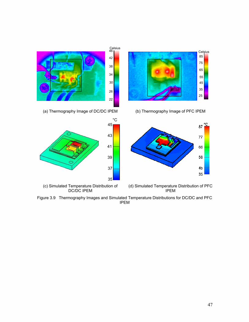
47
(a) Thermography Image of DC/DC IPEM (b) Thermography Image of PFC IPEM
(c) Simulated Temperature Distribution of DC/DC IPEM
(d) Simulated Temperature Distribution of PFC IPEM
Figure 3.9 Thermography Images and Simulated Temperature Distributions for DC/DC and PFC IPEM
46
22
38
42
34
30
26
Celsius
85
25
65
75
55
45
35
Celsius
45°C
41
35
37
39
43

48
Chapter 4 Thermal Behavior Assessment of Integrated Power Electronics
Modules (IPEMs)
The increased heat generation in electronic components can greatly reduce the reliability
of the components and increase the chances of malfunction to the components. A good
understanding of the thermal behavior of these components can help in deciding on an
effective thermal management schemes. To understand their thermal behavior, various
methods should be conducted to analyze the thermal performance of the components.
These analyses can be conducted using finite element thermal modeling as well as
experiments.
Since the finite element models and the thermal boundary conditions varied from
case to case, this section discusses the specific details for each case as well as the
variations in finite element models from the baseline model discussed in section 3.2. In
addition, corresponding experiments for these studies are also discussed. Six studies
were performed in this research to examine various design parameters of the IPEMs that
would possibly affect the thermal performance of the modules. Table 4.1 describes and
lists the objectives of these six studies.
4.1 Study I—Thermal Characterizations
Thermal characterization provides data on the thermal performance of electronic
components. The most common thermal characterization parameter used in
characterizing electronic components is the thermal resistance. This parameter is a
measure of heat flow from the chip to some defined point on the isothermal surface or
ambient under specific environmental conditions. Experimental characterization method
was presented here to obtain the junction-to-ambient thermal resistance, Rja, of the
DC/DC and PFC IPEMs.

49
Table 4.1 Summary of the Case Studies
Study Description Objective
I Thermal Characterization of IPEMs To understand the overall thermal performance of the IPEMs
II Chip-to-chip Distance and Copper Trace Area
To understand the mutual effect among the heating chips
III DBC Ceramic and Ceramic Carrier Materials Selection
To identify better ceramic materials for use to enhance the heat transfer within the IPEMs
IV Metallization Interconnect Patterns, Thickness, and Materials
To understand the metallization design parameters on the ability of transferring heat
within the IPEMs
V Polyimide Thickness To understand the effect of the polyimide thickness on the heat transfer within the IPEMs
VI Integrated Cooling Mechanisms To evaluate and introduce integrated cooling
strategies for improving the thermal performance of the IPEMs
4.1.1 Experimental and Numerical Characterization
The chips were analyzed at different power levels ranging from 0 W to 30 W
experimentally. The experiments were the same as the experiments described in section
3.4. However, only the characterized chip was heated up during the experiments rather
than heating all the chips in the module at the same time as described in the previous
section. Heat generated in the chips took a finite amount of time to propagate from the
junction to the environment surrounding the chips. Therefore, careful attention was given
to the amount of time that power was applied to the device to achieve a reasonable steady
state condition. The relationship between the temperature rise of the chips and the power
loss were then explored. The validated numerical model of the DC/DC and the PFC
IPEM discussed in section 3.3 was also used to characterize the IPEMs numerically in
conjunction to the experiments.
4.1.2 Evaluation of Thermal Resistance Matrix for Multi-chip Modules
A common figure-of-merit used for the comparison of various thermal designs is
the junction-to-ambient thermal resistance, Rja. However, this single parameter cannot
effectively describe the three-dimensional heat flow in multi-chip modules. Sofia [62]
presented a methodology using the superposition method to superimpose the temperature

50
fields for different chips within the multi-chip modules. He also mentioned that this
method is most accurate for applications which are dominated by conduction.
In this method, independent heat sources can be characterized and measured
independently. For a single heat source, the thermal resistance equation can be expressed
as R = ∆T/Q, where R is the junction-to-case thermal resistance, Q is the heat loss, and
∆T is the temperature rise of the heat source. The ∆T can be expressed as ∆T = Ths – Tref,
where Ths is the temperature of the heat source and Tref is the reference temperature. The
reference temperature is referred to a chosen isothermal surface. As Sofia [62] stated,
there is no practical way for specifying the isothermal surface. Therefore, any thermal
resistance based on the fixed temperature surface is specific to the cooling conditions
under which the thermal resistance is determined.
The temperature difference between the heat sources and the case in a multi-chip
module is radically affected by the heat dissipation from the neighboring components, the
heat paths within the module, and the cooling conditions. By using the superposition
method, the junction-to-case thermal resistance for each heat source within the multi-chip
module can be described in a matrix form in Eq. 4.1,
[ ] [ ][ ]Q
T∆R = . (4.1)
For a multi-chip module with ‘N’ number of heat sources, the [R] will be an N x N
matrix. The [Q] and [∆T] matrices will be column vectors. The elements in [∆T]
represent Ti-Tref for i=1st to Nth heat source. For example, a two heat source module will
yield a 2 x 2 thermal resistance matrix in Eq. 4.2:
−−
=
=
⋅
ref2
ref1
2
1
2221
1211
TTTT
T∆T∆
2Q1Q
RRRR
, (4.2)
where ∆T1 is the maximum temperature rise of heat source 1 with only the heat source 1
dissipating heat plus the maximum temperature rise of heat source 1 with only the heat
source 2 dissipating heat. Similarly, ∆T2 is the maximum temperature rise of heat source
2 with only the heat source 1 dissipating heat plus the maximum temperature rise of heat
source 2 with only the heat source 2 dissipating heat.

51
Similarly, the elements in the matrix
2221
1211
RRRR
can be expressed by the
following:
1
ref1111 Q
TTR −= , (4.3)
2
ref1212 Q
TTR −= , (4.4)
1
ref2121 Q
TTR −= , (4.5)
2
ref2222 Q
TTR −= , (4.6)
where T11 is the temperature of heat source 1 with heat dissipation from heat source 1,
T12 is the temperature of heat source 1 with heat dissipation from heat source 2, T21 is the
temperature of heat source 2 with heat dissipation from heat source 1, and T22 is the
temperature of heat source 2 with heat dissipation from heat source 2.
The purpose of this study is to examine the possibility of applying this
methodology to IPEMs as well as examine the error of prediction in predicting the
junction temperatures of the chips in a multi-chip module with a different heat dissipation
rate since the heat transfer within the IPEMs is mainly dominated by conduction. The
numerical model used in this study was the validated DC/DC IPEM model described in
section 3.3 with different boundary conditions. Therefore, the validated interface
conditions and the material properties in the module were not changed in all the cases
discussed in this section.
In this study, the bottom surface of the DBC was defined as an isothermal surface of
50°C to satisfy the imposed fixed reference temperature in Eq. 4.1 and Eq. 4.2 although
the bottom surface might not be an isothermal surface under the real operating conditions.
However, the average temperature on the bottom surface can be taken as the reference
temperature during real operating conditions. The T1 and T2 are determined by the
maximum temperatures of the MOSFET chips in the IPEM.

52
To determine the thermal resistance matrix for the DC/DC IPEM, two cases with
individual heat dissipation of 10 W for both chips were simulated. Different
combinations of heat dissipation for the two chips were also simulated. These results
were used to compare with the predicted results from the calculation using the thermal
resistance matrix obtained earlier.
4.2 Study II—Effect of Chip-to-chip Distance and the Copper Trace Area
Numerical studies were conducted to study the effect of the chip position in the
DC/DC IPEM on the thermal performance of the module. In this study, a simplified
numerical model was created. Since most of the heat from the chips were conducted
through the bottom surface of the chip to the copper traces, from the copper traces to the
DBC ceramic, and to the DBC copper due to the high thermal resistance between the
sides of the chips and the ceramic carrier as well as the top of the chips and the
metallization interconnects, the model created for this study only consisted of the two
chips, the copper traces, the DBC ceramic, and the DBC copper.
The top surfaces of the chips were modeled as adiabatic surfaces. Thus, the heat
from the chips was expected to flow to the bottom surface of the bottom DBC copper.
The bottom surface of the DBC copper was modeled with a heat transfer coefficient of
100,000 W/m2-K at ambient temperature of 20°C so that all of the heat was transferred to
the ambient through the bottom surface of the DBC copper. The minimum size of the
copper trace under each chip in the baseline model was 0.5 mm larger than the chip on all
four sides, which resulted in ~26.8% larger copper trace area than the chip area of ~63.5
mm2.
To study the effect of the chip location and the size of the copper trace on the
thermal resistance of the IPEM, eleven cases were investigated. In the first six cases,
three comparisons were conducted to examine the influence of power loss level of two
chips at 3 mm and 6 mm apart in the x direction as shown in Figure 4.1. The first
comparison evaluated the temperature rise of the models dissipating 5 W each from the
two chips, with chip distance of 3 mm and 6 mm apart, and with the minimum trace area
each. The second comparison compared the models with 10 W heat dissipation from

53
each chip and the third comparison compared the models with 20 W heat dissipation from
each chip.
The model with chip distance of 6 mm apart and 5 W heat dissipation from each
chip was studied for Case 7 to Case 9. These three studies were conducted to study the
effect of enlarging the copper trace area. In Case 7, the copper trace area was expanded
in the x direction by 2 mm as illustrated in Figure 4.2 (a). On the other hand, the copper
trace area was expanded in the y direction by 10 mm as shown in Figure 4.2 (b) in Case
8. Finally, the copper trace area was expanded in both x and y directions by 2 mm and 10
mm respectively in Case 9 (Figure 4.2 (c)). The expansion of the copper trace area in the
x and y directions were mainly restrained by the overall footprint of the DC/DC IPEM.
Based on the current footprint of the DC/DC IPEM, the expansion was limited by 2 mm
in the x direction and 10 mm in the y direction in these studies.
Case 10 and Case 11 examined the location of the chips on the copper trace area
with chip-to-chip distance of 6 mm. In Case 10, MOSFET 1 was maintained at the same
position while MOSFET 2 was moved 10 mm in the –y direction resulted in the chip-to-
chip distance of 1.16 mm in the y direction as shown in Figure 4.3 (a). In Case 11,
MOSFET 1 was moved 2 mm in the –x direction while MOSFET 2 was moved 2 mm in
the +x direction from the position in Case 10. This resulted in the chip-to-chip distance
of 1.16 mm in the y direction and 10 mm in the x direction (Figure 4.3 (b)). The heat
dissipation from the chips was 5 W each in both cases. All eleven cases in this section
are summarized in Table 4.2.
Figure 4.1 Layout for Case 1-6 Studying the Effect of the Chip-to-chip Distance
MOSFET 1 MOSFET2
Copper Traces
DBC Ceramic
Chip-to-Chip Distance
X
Y

54
(a) Copper Trace Area Expansion in x Direction by 2 mm
(b) Copper Trace Area Expansion in y Direction in 10 mm
(c) Copper Trace Area Expansion in x Direction
Figure 4.2 Study on Copper Trace Layout for Case 7-9 with 6 mm Chip-to-Chip Distance
(a) Layout for Case 10—Moved MOSFET 2 (b) Layout for Case 11—Moved MOSFET 1 and MOSFET 2
Figure 4.3 Layouts on Chips Locations for Case 10 and Case 11 with 6 mm Chip-to-Chip Distance
MOSFET 1
MOSFET2
X
Y
1.16 mm
10 mm
MOSFET 1
MOSFET2
X
Y
1.16 mm
6 mm
MOSFET 1 MOSFET2
X
Y
MOSFET 1 MOSFET2
X
Y
MOSFET 1 MOSFET2
X
Y

55
Table 4.2 Parameters Specifications in Investigating the Effects of Chip Locations on the Thermal Performance of DC/DC IPEM
Power Loss (W)
Chip-to-Chip Distance (mm) Copper Trace Area Expansion Moved MOSFET
Case 5 10 20 3 6 In ±x Direction
at 2 mm In -y Direction
at 10 mm MOSFET
1 MOSFET
2
Baseline
1 x x
Study 1
2 x x
3 x x
4 x x
5 x x
6 x x
Study 2
7 x x x
8 x x x
9 x x x x
Study 3
10 x x x x x
11 x x x x x x
4.3 Study III—Selection of DBC Ceramic and Ceramic Carrier Materials
A number of ceramic substrates are available for active IPEMs to form high
density interconnects. In this study, we examined the thermal performance of the PFC
IPEM including alumina, aluminum nitride, and ALOX1™ substrate materials. Three
models with different combinations of ceramic materials were studied and compared to
the baseline model (Case 1) using alumina for the DBC ceramic as well as the ceramic
carrier. In Case 2, an aluminum nitride substrate replaced the alumina substrate as the
ceramic carrier while keeping the alumina DBC ceramic substrate. Similarly, ALOX™
substrate was used in Case 3 to replace the alumina ceramic substrate in Case 1.
ALOX™ substrate features a solid aluminum core and 20 µm thick of oxidized 1 ALOX is a trademark of Micro Components Ltd.

56
aluminum surface for electrical isolation as shown in Figure 4.4. Finally, aluminum
nitride was used for the DBC substrate as well as the ceramic carrier in Case 4. Table 4.3
summarizes the models developed in this study.
Since our interest was in searching for better thermal solutions for the module
itself, the heat sink and the enclosure of the electronic system were not modeled. Instead,
an equivalent convective condition for a fixed heat sink surface area was defined in the
finite element model by defining an overall heat transfer coefficient at the bottom surface
of the DBC copper base. Similarly, the top surface of the module was maintained as an
adiabatic surface as discussed in section 3.2. The heat sink had a size of 73 mm (W) x 73
mm (L) x 32 mm (H) with a 7 mm thick base plate and ten 1.5 mm thick fins. The heat
transfer coefficient on the heat sink was 25 W/m2-K and the ambient temperature was
50°C. The convection from the heat sink to the ambient is defined by Eq. 4.7,
)TT(AhQ ksinss ∞−⋅⋅= , (4.7)
where Q is the total power loss, hs is the average heat transfer coefficient on the heat sink,
As is the total heat convecting area of the heat sink, Tsink is the heat sink temperature, and
T∞ is the ambient temperature. We can then define the overall heat transfer coefficient,
U, at the bottom surface of the DBC copper, ADBC, using Eq 4.8,
DBCss AUAh ⋅=⋅ . (4.8)
The power losses for the heat sources in the model are listed in Table 4.4.
Figure 4.4 Schematic of ALOX™ Substrate
Table 4.3 Models Developed for Studying Different Ceramic Materials
Case Ceramic Material (DBC Ceramic/Ceramic Carrier)
1 (Baseline) Al2O3/ Al2O3 Substrate
2 Al2O3/AlN Substrate
3 Al2O3/ALOX™ Substrate
4 AlN/AlN Substrate
Oxidized AluminumAluminum AluminumOxidized
AluminumDevice

57
Table 4.4 Power Losses Specified in Study III
Heat Source Power Loss (W)
CoolMOS 1 7.8
CoolMOS 2 7.8
SiC Diode 1 4.52
4.4 Study IV—Metallization Layer
In today’s power electronics modules, power semiconductor devices such as
MOSFET chips and IGBT chips are interconnected via wire bonds. This is not suitable
for advanced three-dimensional integration as well as advanced thermal management.
Over the last few years, a planar interconnect technique has been developed to enable the
construction of three-dimensional integrated power electronics modules such as the
metallization bonding used in the IPEMs. While the planar interconnect technique offers
some dominant advantages, reliability issues need more attention because thermo-
mechanical stress can lead to the degradation of the interconnections. Differences in the
coefficient of thermal expansion (CTE) of multi-layers with dissimilar materials expand
and contract at different rates on heating and cooling that lead to thermo-mechanical
failures. In general, these thermo-mechanical failures include defects, cracks, and
peeling of the layers within the module.
To understand the reliability of the metallization layers in Embedded Power
modules, thermally induced stresses in the metallization layers have to be evaluated. The
cohesive failure of the interface delamination between the chips and the deposited
metallization layer can degrade the thermal performance and the reliability of the module.
Thus, a proper design of chip-metallization contact should simultaneously satisfy the
thermal requirement and the mechanical integrity between the chip and the metallization
layer. This section specifically studies (a) the shape and contact areas of the
interconnection on the chip, (b) the metallization thickness, and (c) the material
properties of the metallization.
To reach a better understanding of the thermal and thermo-mechanical behavior
of the metallization layer in Embedded Power modules, the PFC IPEM was chosen as a

58
study case. Both thermal and thermo-mechanical stress simulations were performed
using I-DEAS™. For thermal simulations, the thermal model and the boundary
conditions described in section 4.3 were also used in this study. However, aluminum
nitride was chosen as the ceramic carrier material in the models investigated in section
4.4.1 and 4.4.2. As for the studies in section 4.4.3, aluminum nitride substrate was used
for both the DBC ceramic as well as the ceramic carrier.
The stress simulations were conducted using the structural analysis within I-
DEAS. In embedded power modules, more than 70% of the copper deposition is on top
of the top polyimide layer. Due to the low Young’s modulus of the polyimide, the
polyimide can function as a buffer layer to absorb the thermally induced stress. It was
shown in [71] that the critical stress was on the top surface of the silicon where the two
rigid materials, silicon (chip) and copper (metallization), were in contact. Therefore, only
the silicon chip, the top polyimide layer, and the metallization layer were considered in
the stress model as shown in Figure 4.5 (a). Since the interconnect area had covered 40%
of the SiC diode top area with one 1 mm diameter interconnect via hole on the 1.4 mm x
1.4 mm SiC diode’s top surface, no study was done on the interconnect pattern on the SiC
diodes. Therefore, the focus of this study was only on the interconnect pattern on the
CoolMOS™.
In the stress model, the intrinsic residual stress at 20°C was assumed to be zero
since the metallization layer is electroplated onto the top surface of the silicon at 20°C.
The temperature of the structure was increased from 20°C to 100°C uniformly. The type
of element used for the stress simulations is solid parabolic tetrahedron. A point located
at the center of the bottom surface of the CoolMOS™ chip was fully constrained
(translational and rotational) in all directions. In addition, a point located at the corner of
the chip illustrated in Figure 4.5 (b) was also constrained in the z direction.
(a) Stress Model (b) Boundary Conditions
Figure 4.5 Stress Model and Boundary Conditions for Stress Simulations
X
Z
Y
Device
Metallization Polyimide

59
4.4.1 Metallization Interconnect Patterns
It is believed that large interconnect area between the chip and the metallization
layer can provide higher heat transfer. To investigate the effect of the interconnect
pattern on the thermal performance and the thermal stress, three patterns shown in Figure
4.6 were selected. These patterns were selected based on the current available
interconnect patterns on the chips defined by the chip manufacturers. The first
interconnect pattern had 6 interconnect via holes with diameter of 0.6 mm on the
CoolMOS™ chip. The second interconnect pattern had 9 interconnect via holes with
diameter of 0.6 mm and the third pattern had a rectangular pattern. Table 4.5
summarized the total heat transfer area for each pattern.
(a) 6 Interconnect Via Holes (b) 9 Interconnect Via Holes (c) Rectangular Interconnect Pattern
Figure 4.6 Three Studied Interconnect Patterns: (a) 6 Interconnect Via Holes, (b) 9 Interconnect Via Holes, and (c) Rectangular Interconnect Pattern
Table 4.5 Total Contact Area for the Metallization Layer on the Heat Source for Different Interconnect Patterns
Case Interconnect Pattern Total Contact Area (mm2)
1 6 Interconnect Via Holes 1.7
2 9 Interconnect Via Holes 2.5
3 Rectangular Pattern 9.4
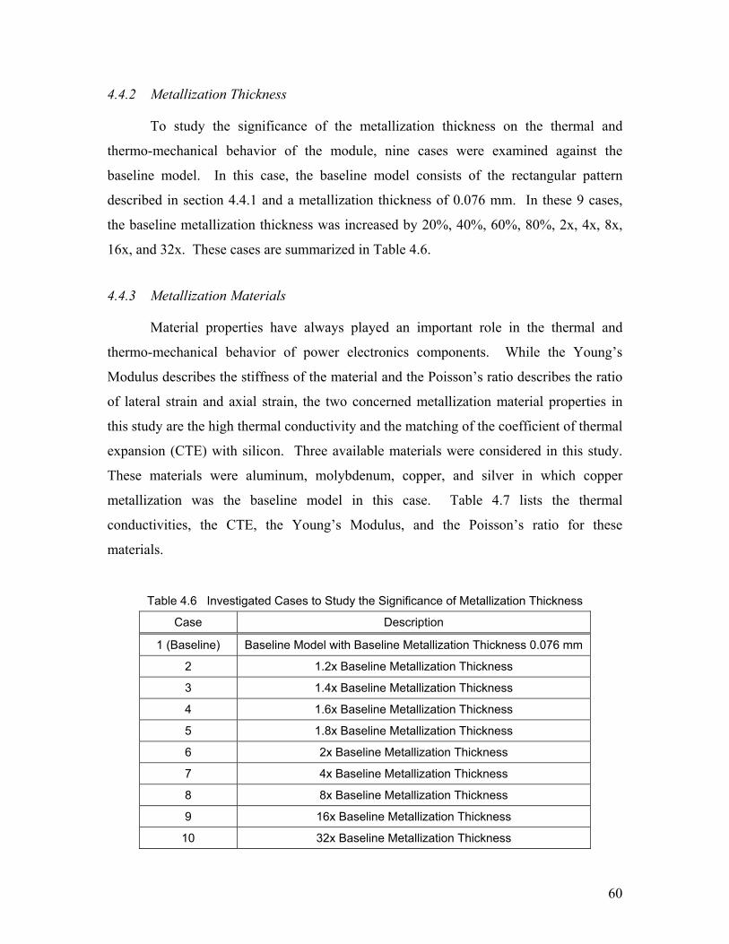
60
4.4.2 Metallization Thickness
To study the significance of the metallization thickness on the thermal and
thermo-mechanical behavior of the module, nine cases were examined against the
baseline model. In this case, the baseline model consists of the rectangular pattern
described in section 4.4.1 and a metallization thickness of 0.076 mm. In these 9 cases,
the baseline metallization thickness was increased by 20%, 40%, 60%, 80%, 2x, 4x, 8x,
16x, and 32x. These cases are summarized in Table 4.6.
4.4.3 Metallization Materials
Material properties have always played an important role in the thermal and
thermo-mechanical behavior of power electronics components. While the Young’s
Modulus describes the stiffness of the material and the Poisson’s ratio describes the ratio
of lateral strain and axial strain, the two concerned metallization material properties in
this study are the high thermal conductivity and the matching of the coefficient of thermal
expansion (CTE) with silicon. Three available materials were considered in this study.
These materials were aluminum, molybdenum, copper, and silver in which copper
metallization was the baseline model in this case. Table 4.7 lists the thermal
conductivities, the CTE, the Young’s Modulus, and the Poisson’s ratio for these
materials.
Table 4.6 Investigated Cases to Study the Significance of Metallization Thickness
Case Description
1 (Baseline) Baseline Model with Baseline Metallization Thickness 0.076 mm
2 1.2x Baseline Metallization Thickness
3 1.4x Baseline Metallization Thickness
4 1.6x Baseline Metallization Thickness
5 1.8x Baseline Metallization Thickness
6 2x Baseline Metallization Thickness
7 4x Baseline Metallization Thickness
8 8x Baseline Metallization Thickness
9 16x Baseline Metallization Thickness
10 32x Baseline Metallization Thickness

61
Table 4.7 Generic Material Properties at 300K for the Study on Metallization Materials
Material Thermal Conductivity (W/m-K) CTE (µm/m-C) Young’s Modulus
(GPA) Poisson’s
Ratio
Aluminum 170 23.5 69 0.33
Copper (Baseline) 395 16.4 110 0.34
Molybdenum 138 6 330 0.32
Silver 410 19.9 76 0.39
Silicon 118 2.22 185 0.28
Polyimide 0.3 10 14 0.35
4.5 Study V—Significance of Polyimide Layer
Polyimide layers were added to the IPEMs for electrical insulation as well as
providing planarity for depositing the next layer in the packaging process. The thickness
of the polyimide is highly constrained by the available thin-film technology during the
IPEMs packaging process. A thick polyimide layer can result in high thermal resistance
and increase module thermal resistance. In this study, the effect of the polyimide
thickness on the thermal performance of the IPEMs was studied. Current polyimide
thickness is 0.127 mm for both layers illustrated in Figure 3.3 (b). The smaller the
polyimide thickness, the smaller the particular layer will contribute on the overall
package thermal resistance.
In this study, a reduced polyimide thickness of 0.02 mm was investigated. In
Case 1, the thicknesses of both polyimide layers were reduced from 0.127 mm to 0.02
mm. To further identify the polyimide layer that has a larger influence on the thermal
performance of the active IPEMs, two other cases were studied. In Case 2, only the
thickness of the top polyimide layer was reduced while keeping the thickness of the
bottom polyimide layer at 0.127 mm. In contrast, only the thickness of the bottom
polyimide layer was reduced in Case 3. The thermal model and the boundary conditions
described in section 4.3 were also used in this study. In all three cases, an aluminum
nitride ceramic substrate was used for the DBC ceramic and the ceramic carrier.

62
4.6 Study VI—Evaluation of Integrated Cooling Mechanisms for IPEMs
As a general trend in power electronics, packaging is shrinking and more
functionality is integrated into closely packed structures, thus increasing the demands on
the thermal management of power electronics. Recognizing the inherent need for the
thermal design of the active IPEMs, this section presents some of the thermal
management options which will lead to the achievement of integrated cooling
mechanisms in the active IPEMs.
There are many different approaches for achieving such integrated cooling. These
strategies include the employment of integrated heat pipes, radiant cooling, or better
interface materials. To achieve integrated cooling in the structure of the active IPEMs,
this research investigated several possible integrated thermal management options. We
first identified the heat path within the structure of the active IPEMs. With known
hotspots and high thermal resistance heat paths, we worked on various ways to reduce the
hotspots by reducing the thermal resistances in the major heat paths. The baseline model
in this study refers to the model described in section 3.2 in which alumina substrates were
used as the DBC ceramic as well as the ceramic carrier.
4.6.1 Structural Enhancement
To create an additional heat path from the hotspot to the ambient, an alumina
substrate was added to the IPEM structure from the top of the metallization on top of the
SiC diode 1 to the DBC copper trace in the first studied case. In the second case, an
alumina substrate was connected from the top of the metallization on the SiC diode 1 to
the heat sink. It is important to remember that any modification to the IPEM structure
can change the characteristic of the IPEMs in the aspects of the electrical, mechanical and
thermal performances. Figure 4.7 shows the structural enhancements investigated in this
study.
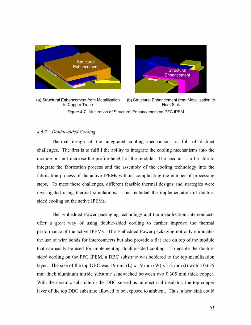
63
(a) Structural Enhancement from Metallization to Copper Trace
(b) Structural Enhancement from Metallization to Heat Sink
Figure 4.7 Illustration of Structural Enhancement on PFC IPEM
4.6.2 Double-sided Cooling
Thermal design of the integrated cooling mechanisms is full of distinct
challenges. The first is to fulfill the ability to integrate the cooling mechanisms into the
module but not increase the profile height of the module. The second is to be able to
integrate the fabrication process and the assembly of the cooling technology into the
fabrication process of the active IPEMs without complicating the number of processing
steps. To meet these challenges, different feasible thermal designs and strategies were
investigated using thermal simulations. This included the implementation of double-
sided cooling on the active IPEMs.
The Embedded Power packaging technology and the metallization interconnects
offer a great way of using double-sided cooling to further improve the thermal
performance of the active IPEMs. The Embedded Power packaging not only eliminates
the use of wire bonds for interconnects but also provide a flat area on top of the module
that can easily be used for implementing double-sided cooling. To enable the double-
sided cooling on the PFC IPEM, a DBC substrate was soldered to the top metallization
layer. The size of the top DBC was 19 mm (L) x 19 mm (W) x 1.2 mm (t) with a 0.635
mm thick aluminum nitride substrate sandwiched between two 0.305 mm thick copper.
With the ceramic substrate in the DBC served as an electrical insulator, the top copper
layer of the top DBC substrate allowed to be exposed to ambient. Thus, a heat sink could
Structural Enhancement
Structural Enhancement

64
be brazed to the top as well as the bottom surface of the PFC IPEM. In addition, other
advanced cooling methods such as liquid cooling, spray cooling, and jet impingement can
also be implemented on the top surface of the module to achieve the double-sided cooling
effect. Figure 4.8 illustrates the concept of double-sided cooling for an active IPEM.
To investigate the significance of the top DBC on the double-sided cooling effect,
two finite element models were created to examine several commercially available
ceramic substrate materials for the top DBC. Again, these ceramic substrates were
alumina ceramic and aluminum nitride ceramic substrates. In addition to DBC, Thermal
Clad2™ substrates were also investigated in exploring better substrate for top side
cooling. The Thermal Clad™ substrate is an insulated metal substrate3™ (IMS) with
three layers: aluminum or copper base, dielectric layer, and circuit layer illustrated in
Figure 4.9. The material properties and the thickness of the individual layer in the
Thermal Clad are summarized in Table 4.8.
Figure 4.8 Illustration of Double-sided Cooling for an Active IPEM
2 Thermal Clad is a trademark of The Bergquist Company 3 IMS is a trademark of Sanyo Electric Co., Ltd.
Heat Sink Forced-air Cooling / Liquid Cooling / Jet Impingement
Top DBC
Bottom DBC
EpoxyPolyimide
Heat SourcePolyimide Polyimide
Copper
Epoxy CeramicCeramic
Metallization
Solder Polyimide
Heat Sink Forced-air Cooling / Liquid Cooling / Jet Impingement
Solder

65
Figure 4.9 Schematic of Thermal Clad™ Substrate
Table 4.8 Material Properties of Thermal Clad™
Layer Material Thermal Conductivity (W/m-K) Thickness (µm)
Circuit Copper 388 35
Dielectric Bergquist 3 75
Aluminum 167 1000 Base
Copper 388 1000
Table 4.9 lists the four models investigated in this study. The finite element
models created in this study were similar to the finite element models described in section
4.3. Both the bottom DBC surface and the top DBC surface were modeled as an
equivalent convective condition of 25 W/m2-K for a fixed heat sink surface area at
ambient temperature of 50°C. Since the top DBC surface was smaller than the bottom
DBC surface, the heat sink brazed on the top DBC was also relatively smaller than the
bottom heat sink.
4.6.3 Assessment on Double-sided Cooling Experimentally
In addition to the numerical studies described in section 4.6.2, experiments were
also conducted to study the advantages of double-sided cooling for IPEMs. By using the
similar experiment setup described in section 3.2, three different cases were studied using
DC/DC IPEM. Two prototypes were fabricated for the experiments. The first prototype,
Module A, was the original DC/DC IPEM. The second prototype, Module B, had
additional DBC substrate soldered onto the top of the DC/DC IPEM. Module B was also
used in the third case study by adding additional heat spreaders on both the top and
Aluminum / Copper Base
Dielectric LayerCircuit Layer

66
bottom of the module. Interface material, Sarcon4® thermal gap filler pads with thermal
conductivity of 7 W/m-K, were placed between the prototype and the heat spreaders to
enhance the heat transfer from the module to the heat spreaders. Figure 4.10 shows the
prototypes for all three cases.
In all three experiments, one thermocouple was placed at the inlet of the wind
tunnel to measure the ambient temperature. To avoid disturbance of the heat flow within
the modules, no thermocouples were embedded into the modules. In Case I, two
thermocouples were attached on the backside of the module as shown in Figure 4.11 (a).
On the other hand, three thermocouples were attached on the backside of the module in
the second experiment as illustrated in Figure 4.11 (b). Finally, six thermocouples were
used in the third experiment to obtain real-time temperature of the module at different
locations (Figure 4.11 (c)). To avoid the effect of heat sink on the heat transfer from the
module to the ambient, no heat sink was used in all three experiments. To ensure equal
airflow on both the top and bottom surfaces of the module, the module was placed at the
center of the wind tunnel supported by an insulated stand as shown in Fig. 4.12.
(a) DC/DC IPEM for Case I (b) DC/DC IPEM for Case II (c) DC/DC IPEM for Case III
Figure 4.10 Prototypes for Double-sided Cooling Experiments
4 Sarcon is a registered trademark of Fujipoly
Copper Metallization Top DBC Heat Spreader
DC/DC IPEM
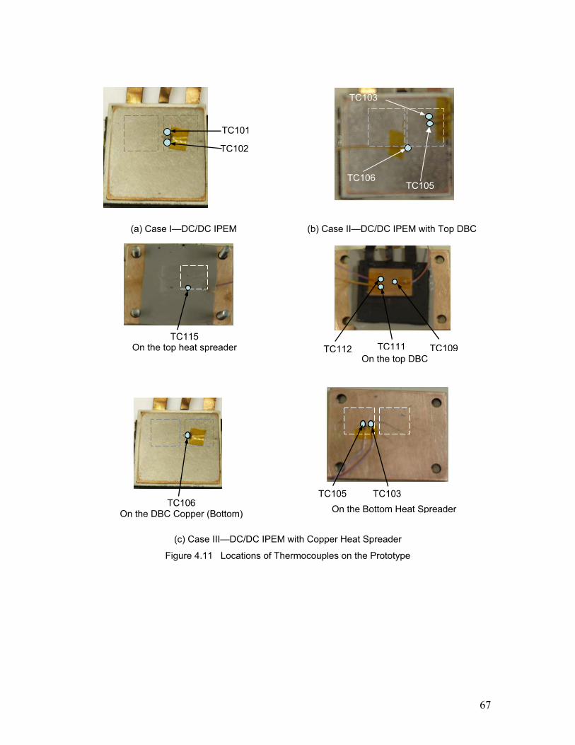
67
(a) Case I—DC/DC IPEM (b) Case II—DC/DC IPEM with Top DBC
(c) Case III—DC/DC IPEM with Copper Heat Spreader
Figure 4.11 Locations of Thermocouples on the Prototype
TC103
TC105 TC106
TC101
TC102
TC115 On the top heat spreader
On the top DBC TC109TC112 TC111
TC106 On the DBC Copper (Bottom) On the Bottom Heat Spreader
TC105 TC103

68
Figure 4.12 Placement of the Module during Experiment
4.6.4 Micro-channel Cooling
With heat loss density continues to rise, micro-channel liquid cooling has become
a major consideration in the thermal management of electronic components. Cooling
liquid is pumped through the micro-channels to remove the heat from the electronic
components. High heat transfer coefficients can be achieved in micro-channel cooling by
either increasing the liquid flow rate or decreasing the hydraulic diameter. Micro-
channel liquid cooling offers additional benefit of superior liquid thermal properties
compared to forced-air cooling. However, this application is limited by the pumping
power limit due to the high pressure drop. A preliminary study on the micro-channel
cooling was conducted in this research to assess the advantages of using micro-channel
cooling for IPEMs.
The advantages of the additional DBC soldered onto the metallization have been
discussed in section 4.6.2. However, additional advantage can be obtained by
implementing liquid cooling on the top side of the top DBC. To further reduce the
temperature rise of the hotspots within the PFC IPEM, implementation of liquid cooling
on the top side of the top DBC was studied. To attain integrated cooling mechanism
within the module, two different ways of implementing micro-channel on the module
were studied using finite element modeling.
Wind Tunnel
Honeycomb
Test Prototype Insulated Stand

69
The first study employed a copper cap with etched channels in the copper cap for
liquid cooling as illustrated in Figure 4.13. This copper cap covered the top side of the
module as well as connected to the bottom heat spreader. Six channels with diameter of
1.5 mm and 50 mm long were created in the copper cap and covered the top surface area
of the module. In this study, the finite element model was similar to the one described in
section 4.3 with the same convection condition on the bottom surface of the DBC.
However, the equivalent heat transfer coefficient was defined on the bottom surface of
the copper heat spreader rather than the DBC with adjusted value based on the bottom
surface area of the copper heat spreader. The size of the heat spreader was 38 mm (L) x
50 mm (W) x 3 mm (t). On the other hand, the top surface of the copper cap was defined
with a heat transfer coefficient of 25 W/m2-K. The ambient temperature was maintained
at 50°C. In this study, the liquid flowed in the channels from one side and exited from
the other side of the channels. The inlet condition was defined with a pressure rise of 12
kPa while the outlet of the channels was vented to the ambient condition. The specified
boundary conditions are illustrated in Figure 4.13. Water was used as the coolant in this
study.
Figure 4.13 Illustration of Copper Cap for the PFC IPEM
Heat Spreader
Copper Cap
Channels
Inlet Condition: Pressure Rise of
12 kPa
Outlet Condition: Vent to Ambient

70
To further investigate the effect of liquid cooling on the improvement in the
thermal performance of the module, an additional channel layout was also studied. In
this second case, the channel layout in Case 1 was modified. Two channels were laid on
top of the heat sources, the CoolMOS™ chips and the SiC diode, within the copper cap
as illustrated in Figure 4.14. In this case, the inlet liquid condition was modeled with a
constant volume flow rate of 0.0003 m3/s while the outlet was vented to the ambient of
50°C. Again, the channels had a diameter of 1.5 mm. The top surface of the copper cap
was defined with a heat transfer coefficient of 25 W/m2-K.
Figure 4.14 Illustration of Channels on Top of Hotspots for the PFC IPEM
Heat Spreader
Channels
Inlet Condition: 0.0003 m3/s
Inlet Condition: 0.0003 m3/s
Outlet Condition: Vent to Ambient

71
Chapter 5 Results and Discussions
Independent of its application, the hottest part in any electronic system most likely is
going to be the semiconductor chip. The trend towards increasing heat flux at the module
level is continuing. The desire to increase performance by reducing the chip operating
temperatures creates a further challenge in the thermal designs. Most of the
semiconductor bare chips can be packaged using different packaging technologies such
as commonly used QFPA, BGA, and PGA. While the thermal behaviors of these
packages are well studied, this research chose to focus on studying the thermal behavior
of an innovative packaging technology—Embedded Power.
Since that majority of the thermal resistance of the junction-to-ambient in many
common environments is within the package itself, understanding of the role of the
package is critical for determining the thermal behavior of the module, especially the
effects on the junction temperature. In addition, a good understanding on the package
can also help in redesigning the package for better thermal performance, thus reducing
the package thermal resistance. While the goals of the studies described in Chapter 4
were to have better understanding on the thermal behavior of the Embedded Power
modules, this chapter discusses the results from the studies and provides an insight on the
thermal behavior of the Embedded Power modules.
5.1 Thermal Characterization
5.1.1 Experimental and Numerical Characterization
Repeated tests were performed to ensure the reproducibility of the experimental
measurements before recording the actual data. Ten readings were taken at each power
level. The performance characteristics of the chips in the DC/DC IPEM are presented in
the form of chip temperature rise, ∆T, versus power loss. The temperature rise is defined

72
as ∆T = Tmax-Tinlet, where Tmax is the maximum die temperature and Tinlet is the inlet air
temperature.
In the power loss range from 0 W to 30 W, the corresponding maximum
temperature rise for the chips of the DC/DC and the PFC IPEM are shown in Figure 5.1
and Figure 5.2 respectively. A line is fitted through the collected data to represent the
relationship between the chip temperature rise and the power loss. The slope of the fitted
line characterizes the thermal resistance from the chip to the ambient, Rja. Table 5.1
summarizes the Rja of the chips in DC/DC and PFC IPEMs. We can see from Table 5.1
that the Rja of MOSFET 2 is larger than MOSFET 1 while both MOSFET chips have the
same material properties. Therefore, it is believed that the location of the chips in the
DC/DC IPEM can affect the Rja of the two similar MOSFET chips in a module.
Similarly, the Rja of the SiC diodes are larger than the CoolMOS™ chips simply because
the conduction area of the SiC diodes is much smaller than the CoolMOS™ chips; thus
increasing the thermal resistance of the solder interface between the SiC diodes and the
copper trace as well as the epoxy interface between the SiC diodes and the ceramic
carrier. From the results summarized in Table 5.1, the users can predict the maximum
temperature of the chips with the desired power loss under forced air cooling or for a
given maximum operating temperature.
Figure 5.1 Thermal characterization of DC/DC IPEM
y = 1.8987x (MOSFET 1)
y = 2.5709x (MOSFET 2)
0
10
20
30
40
50
60
70
0 5 10 15 20 25 30
MOSFET 1
MOSFET 2
Power Loss (W)
Tem
p. R
ise,
Tm
ax-T
inle
t (°C
)
R2 = 0.9179
R2 = 0.9648
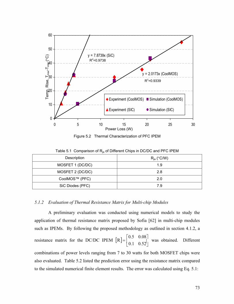
73
Figure 5.2 Thermal Characterization of PFC IPEM
Table 5.1 Comparison of Rja of Different Chips in DC/DC and PFC IPEM
Description Rja (°C/W)
MOSFET 1 (DC/DC) 1.9
MOSFET 2 (DC/DC) 2.8
CoolMOS™ (PFC) 2.0
SiC Diodes (PFC) 7.9
5.1.2 Evaluation of Thermal Resistance Matrix for Multi-chip Modules
A preliminary evaluation was conducted using numerical models to study the
application of thermal resistance matrix proposed by Sofia [62] in multi-chip modules
such as IPEMs. By following the proposed methodology as outlined in section 4.1.2, a
resistance matrix for the DC/DC IPEM [ ]
=
52.01.008.05.0
R was obtained. Different
combinations of power levels ranging from 7 to 30 watts for both MOSFET chips were
also evaluated. Table 5.2 listed the prediction error using the resistance matrix compared
to the simulated numerical finite element results. The error was calculated using Eq. 5.1:
y = 2.0173x (CoolMOS)
y = 7.8739x (SiC)
0
10
20
30
40
50
60
0 5 10 15 20 25 30
Experiment (CoolMOS) Simulation (CoolMOS)
Experiment (SIC) Simulation (SIC)
Tem
p. R
ise,
Tm
ax-T
inle
t (°C
)
Power Loss (W)
R2=0.9339
R2=0.9738

74
%100TT
TTError%
refsim
matrixsim ×−−
= , (5.1)
where Tsim is the maximum temperature of the chip from the simulated numerical model,
Tmatrix is the predicted junction temperature of the chip using the resistance matrix, and
Tref is the reference temperature. The results show that the predicted errors range from
1.5% to 21% with average of 5.5% depending on the heat dissipation levels of the two
heat sources.
It is also observed that the maximum temperature of MOSFET 2 can be predicted
more accurately than MOSFET 1. A higher error (21%) was obtained when the heat
dissipation from MOSFET 1 was much lower than MOSFET 2 (MOSFET 1:10 W,
MOSFET 2:30 W). This is mainly because of the non-symmetrical heat source location
in the module and because the positions of the two heat sources in the module skewed
more towards MOSFET 1. While maintaining the heat dissipation from MOSFET 1 at 10
W, the thermal resistance matrix under predicted the temperature of MOSFET 1 and over
predicted the temperature of MOSFET 2 when increasing the heat dissipation from
MOSFET 2. On the other hand, the thermal resistance matrix over predicted the
temperature of MOSFET 1 and under predicted the temperature of MOSFET 2 when
increasing the heat dissipation from MOSFET 1 while maintaining the heat dissipation
from MOSFET 2 at 10 W. It is also observed that keeping the heat dissipation from
MOSFET 1 at 30 W while increasing the heat dissipation from MOSFET 2 will increase
the prediction error for both MOSFET chips but higher error will occur on MOSFET 2
than MOSFET 1.
Table 5.2 Prediction Errors Using Thermal Resistance Matrix
Heat Losses (W) Temperature for MOSFET 1 (°C) Temperature for MOSFET 2 (°C)
MOSFET 1 MOSFET 2 Simulated Error Prediction Simulated Error Prediction
30 30 66.81 +3.5% 67.19 +8.2%
30 20 66.12 +3% 62.57 +6.6%
30 10 65.53 +1.7% 58.37 -2%
20 30 62.59 -1.5% 66.55 +6.3%
10 30 59.36 -20.9% 65.98 +3.9%
12 7 56.39 +2.7% 54.6 +5.2%

75
While the resistance matrix works well for symmetrical heat dissipation in multi-
chip modules, the resistance matrix can still predict the temperature rise of
nonsymmetrical heat dissipation multi-chip modules such as DC/DC IPEM within an
acceptable error margin of 5% to 10% in average in the heat dissipation range of 10 W to
30 W. Again, it is important to remember that this method only works for conduction
dominant scenarios and the reference temperature should be carefully defined.
5.2 Effect of Chip-to-chip Distance and Copper Trace Area
Six cases were conducted to study the effect of chip-to-chip distance and different
power loss levels on the thermal performance of the simplified model of DC/DC IPEM.
Figure 5.3 shows the results for case 1 to case 6. The results show that the maximum
temperature rise of the chips at different power loss levels is independent of the distance
between the two heat sources in the x direction with the minimum copper trace area. In
the second study, the copper trace area was expanded in both x and y directions while
maintaining the chip-to-chip distance in the x direction to be 6 mm and heat dissipation
of 5 W from each MOSFET.
Figure 5.4 shows that expanding the copper trace in the x direction has more of a
significant effect than expanding the copper trace area in the y direction. Expanding the
copper trace area in the x direction increased the trace area by 48.9% and improved the
maximum temperature rise of the MOSFET by 0.8%. On the other hand, expanding the
copper trace area in the y direction doubled the trace area but only improved the
maximum temperature rise by 0.3%. Overall, expanding the copper trace area in both
directions can reduce the temperature rise of the MOSFET by 1.1%, which is the
combined improvement in case 7 and case 8.
To further study the influence of the chip-to-chip distance, two different
MOSFET locations were investigated and compared to case 1. Figure 5.5 shows that
moving MOSFET 2 to the other end of the copper trace does not further reduce the
temperature rise of the heat sources from case 8. However, moving the heat sources in
the x direction can slightly reduce the maximum temperature rise of the MOSFET by
0.6% compared to case 1.

76
Figure 5.3 Results for Case 2-6 in Study 1 Compared With Case 1 (Baseline)
Figure 5.4 Thermal Improvements for Case 7-9 in Study 2 Compared to Case 1 (Baseline)
33.28 33.27
43.0843.11
36.5436.55
05
101520253035404550
Case 1 Case 2 Case 3 Case 4 Case 5 Case 6
Tem
pera
ture
Ris
e (°
C)
0.8%
1.1%
0.3%
0.0%
0.2%
0.4%
0.6%
0.8%
1.0%
1.2%
Case 7 Case 8 Case 9
Impr
ovem
ent O
ver C
ase
1 (%
)

77
Figure 5.5 Thermal Improvements for Case 10 and Case 11 in Study 3 Compared to
Case 1 (Baseline)
From this study, we learn that the chip-to-chip distance in the DC/DC IPEM is an
insignificant factor in improving the thermal performance of the module. Although one
might think that enlarging the copper trace area would significantly spread the heat from
the heat source, the results show that only expanding the copper trace area in the x
direction slightly helps in spreading the heat better compared to the copper trace
expansion in the y direction as shown in Figure 5.6. Therefore, the total copper trace area
does not always improve the heat spreading and the direction of expanding the copper
trace area matters.
Figure 5.6 Temperature Contour for Case 9 in Study 2 on Table 4
50.0
50.6
51.2
51.8
52.9
52.3
°C
MOSFET 1 MOSFET 2
Copper Trace
DBC Ceramic
0.3%
0.6%
0.0%
0.1%
0.2%
0.3%
0.4%
0.5%
0.6%
0.7%
Case 10 Case 11
Impr
ovem
ent O
ver C
ase
1 (%
)

78
5.3 Selection of DBC Ceramic and Ceramic Carrier Materials
High thermal conductivity ceramic has always promised a better thermal
performance in the thermal management of electronics. However, the use of the high
thermal conductivity ceramic does not always result in better thermal performance
especially in multi-layer structure where the heat path is usually more complex.
Therefore, this study investigates the combinations of different ceramic materials for the
DBC ceramic and the ceramic carrier. Figure 5.7 compares the results for four cases
described in section 4.3. Aluminum nitride and ALOX™ substrates provide ~3%
improvement in the thermal performance over the alumina substrate for the ceramic
carrier although the thermal conductivity of the aluminum nitride and ALOX™ are about
six times higher than alumina. This is mainly due to the high thermal resistance of the
epoxy between the device and the ceramic carrier.
Overall, the results show that having high thermal conductivity of the DBC
ceramic is more beneficial than increasing the thermal conductivity of the ceramic
carrier. This is mainly because most of the heat is dissipated through the DBC substrate
to the heat sink. Thus, case 4 with aluminum nitride for both DBC ceramic and ceramic
carrier demonstrated the best combination of ceramic materials for the DBC ceramic and
the ceramic carrier with 9% improvement over the baseline model (alumina substrate for
DBC ceramic and ceramic carrier).
5.4 Metallization Layer
5.4.1 Metallization Interconnect Patterns
In this study, three different patterns were investigated. Figure 5.8 shows the
temperature rise of the CoolMOS™ chips and the von Mises stress for each pattern.
Although case 2 (9 interconnect via holes) has 50% more area in contact between the
silicon die and the metallization than case 1 (6 interconnect via holes), both the
temperature rise and the von Mises stress did not show significant improvement over case
1. However, increasing the contact area from 2.4 mm2 (case 2) to 9.4 mm2 (~3.9x) of
case 3 reduced the temperature rise by 3.9% and reduced the stress on the metallization

79
by 6.4%. On the other hand, the von Mises stress on the silicon die increased by ~3.5%
by replacing case 2 with case 3.
Figure 5.7 Results Comparison for Different Ceramic Materials
Figure 5.8 Temperature Rise and Maximum von Mises Stress for Three Different Interconnect Patterns
Tem
pera
ture
Ris
e (°
C)
05
101520
2530354045
CoolMOS 1 CoolMOS 2 SiC 1
Al2O3/Al2O3 Al2O3/AlN
Al2O3/ALOX AlN/AlN
0
50
100
150
200
6 Via Holes 9 Via Holes Rectangular Pattern
Temp. on CoolMOS 1Temp. on CoolMOS 2Stress on Silicon DieStress on Metallization
Tem
p. R
ise
(°C
) or M
ax. v
on M
ises
S
tress
(MP
a)

80
Figure 5.9 shows the stress distributions on the silicon die and the metallization
while Figure 5.10 shows the temperature distribution on the metallization layer. It is
observed from the stress distributions that higher stress was formed at the edge of the
pattern on the silicon die and more towards the center of the pattern on metallization.
The temperature distribution shows that the heat was conducted from the silicon die to
the metallization through the interconnect pattern. However, the heat spreading
resistance was high and thus heat could not transport across the metallization effectively.
Overall, the thermomechanical stress is not very sensitive to the patterns with 6
interconnect via holes and 9 interconnect via holes. Therefore, the rectangular pattern
(case 3) demonstrates better choice among the three studied patterns thermally and
thermo-mechanically.
Stress on Silicon Stress on Metallization
(a) 6 Holes (Case 1) (b) 6 Holes (Case 1)
(c) 9 Holes (Case 2) (d) 9 Holes (Case 2)
(e) Rectangular (Case 3)
(f) Rectangular (Case 3)
Figure 5.9 Stress Distribution on Top of the Silicon Die and Bottom of Metallization
N/mm2
91
58
25
190
157
124
N/mm2
53
29
5
125
101
77

81
Figure 5.10 Temperature Distribution on the Metallization for 6 Holes Pattern
5.4.2 Metallization Thickness
Different metallization thicknesses were also investigated to understand the effect
of the thickness on the thermal performance and thermomechanical stress of the
Embedded Power modules. In this study, the original metallization thickness (0.076 mm)
was increased by 20%, 40%, 60%, 80%, 2x, 4x, 8x, 16x, and 32x (case 1-case10 in Table
4.6).
Figure 5.11 shows the impact of the metallization thickness on the thermal
performance and the thermomechanical behavior of the module. The temperature rise of
the module decreases with the increase in the metallization thickness. Despite this, the
maximum von Mises stress on the metallization increases with the increase in the
metallization thickness. However, the temperatures of the CoolMOS chips are not as
sensitive as the temperature of the SiC diode to the change in the metallization thickness.
On the other hand, the stresses on the silicon die and the metallization show a significant
change only after increasing the metallization thickness by 16x. This metallization
thickness, however, is unrealistic from the viewpoint of processing, as well as the
necessary electrical interconnect resistance.
Figure 5.12 shows the stress distributions on the metallization with baseline
thickness (case 1), 4x increase in thickness (case 7), and 16x increase in thickness (case
9). It can be observed from the stress distributions that the high stress areas shifted from
76.6°C
73.6
70.6
67.5
64.5

82
the center of the interconnect pattern in case 1 (baseline thickness) towards the edge of
the pattern with the increase in the metallization thickness.
Figure 5.11 Temperature Rise and Maximum von Mises Stress for Different Metallization
Thicknesses
(a) Model III (b) Model IX
(c) Model XI
Figure 5.12 von Mises Stress Distributions on Metallization for Baseline Thickness, 4x Thickness, and 16x Thickness
155 N/mm2
139
123
107
91
75
-30
-20
-10
0
10
20
30
40
50
60
1.2x 1.4x 1.6x 1.8x 2x 4x 8x 16x 32x
Temp. on CoolMOS 1 Temp. on CoolMOS 2
Temp. on SIC 1 Stress on Cu
Stress on Si
Metallization Thickness Relative to Baseline Thickness
Cha
nge
in P
erce
ntag
e w
ith re
spec
t to
Base
line
Mod
el (C
ase
1) (%
)

83
5.4.3 Metallization Materials
The material used for the metallization layer plays an important role in
determining the significance of the metallization in transporting heat away from the
active devices as well as reliability issues such as possible delamination of the
metallization layer. Copper, molybdenum, aluminum, and silver were compared in this
study. The material properties for these materials were listed in Table 4.7.
The result in Figure 5.13 shows that using molybdenum as the metallization
material results in the lowest stress compared to other materials due to the good match of
CTE between other molybdenum and silicon. On the other hand, molybdenum shows the
highest temperature rise among the compared materials due to its low thermal
conductivity. Compared to copper, molybdenum resulted in 4.7% higher temperature rise
but 41% less in stress than copper. Therefore, molybdenum is a good candidate to
replace the copper metallization layer from a thermomechanical perspective.
Figure 5.13 Trade-offs Between Thermal Performance and Thermomechanical Behavior for
Different Materials
28 28 27 2840 40 38 38
68
182
148
170
2727272727272728
3638
100102104
53
0
50
100
150
200
250
138 170 395 410 500 1000
Temp on CoolMOS 1 Temp on CoolMOS 2Temp on SIC 1 Stress on CuStress on Si
Max
. Tem
p. R
ise
(°C
) or M
ax. v
on M
ises
S
tress
(MPa
)
(Mo) (Al) (Cu) (Ag)Thermal Conductivity (W/m-K)

84
Although silver has the highest thermal conductivity among the studied materials,
the improvement in thermal performance would not outperform molybdenum and copper
due to its higher CTE mismatch with silicon compared to molybdenum and copper.
Overall, the worst material to be used is aluminum because of its low thermal
conductivity and highest CTE mismatch with silicon.
Further study was conducted to understand the impact of thermal conductivity of
the metallization layer on improving the heat transport through the metallization layer.
Thus, the study extended the thermal conductivity values to any material with thermal
conductivity values of 500 W/m-K and 1000 W/m-K. Since no specific materials with
these thermal conductivity values (i.e., no known CTE values) were specified, the stress
analysis was not investigated for these two cases. It is shown in Figure 5.13 that the
maximum temperature rise can be further reduced by as much as ~6% when increasing
the thermal conductivity from 410 W/m-K to 1000 W/m-K. Figure 5.13 also shows that
the temperatures of CoolMOS™ chips were not sensitive to the thermal conductivity of
the metallization.
5.4.4 Specification of Restraints on Stress Models
Boundary conditions always play a crucial role in finite element modeling.
Inaccurate boundary conditions can result in false simulation results. In the modeling of
the thermomechanical behavior, the defined restraints on the finite element model should
accurately resemble the actual condition. In the stress model of the IPEM, several
possible restraints can be used to mimic the actual condition in analyzing the thermo-
mechanical behavior of the IPEM. Therefore, these constraints were explored to examine
the influence on the simulation results.
The stress models used in the study of the metallization layer are described in
section 4.4. In addition to the restraints described in Figure 4.5, three other restraints
were also studied to check the sensitivity of the stress results on different boundary
conditions. The points of interest for specifying the constraints include the four corner
points as well as the center point on the bottom surface of the silicon. Figure 5.14 shows
the possible points for defining the constraints in the stress model.

85
Three different sets of restraints on the possible locations in the stress model were
investigated. While the first restraint set is used in the three studies discussed in section
5.4, the second set of restraint involved constraining point V1 in the x direction, point V2
in both x and y direction, and point V3 in all three directions. In the third restraint set,
point V1 is constrained in y and z direction, point V2 is constrained in the z direction,
and point V4 is restrained in all three directions. Finally, all four points are constrained
in z direction only in restraint set 4. Table 5.3 summarized these four restraint sets.
Figure 5.14 Possible Locations for Restraints Specification in Stress Model
Table 5.3 Combination of (Translational and Rotational) Restraints Specified for the Stress Model
Restraint Restraint at Center Point
Restraint at V1
Restraint at V2
Restraint at V3
Restraint at V4
1 x, y, z z
2 x x, y x, y, z
3 y, z z x, y, z
4 z z z z
X
Z
YV2
V1
V4
V3

86
The maximum average von Mises stress on both the silicon and metallization are
compared in Table 5.4. Although all these four combinations of restraints are different
from each other, the simulated von Mises stress on both the silicon and the metallization
layer does not vary within 5%. Further study on the stress distribution also shows that
the stress distribution does not change with these different constraints. Figure 5.15 shows
the stress distribution on the silicon for the first three restraint sets.
5.5 Significance of Polyimide Layer
Figure 5.16 shows the temperature rise of the heat sources with respect to the
change in the thickness of the polyimide layers described above for the all three cases
studied in section 4.5. The result shows that reducing both the top and bottom polyimide
thickness can further reduce the maximum temperature of the active IPEM by ~5% and
the improvement is more evident on the SiC diodes than the CoolMOS™ chips. In
addition, reducing the thickness of the top polyimide layer has a more significant
improvement than reducing the thickness of the bottom polyimide layer (3.3% vs. 0.6%)
on the SiC diode 1. This is mainly because the heat path from the heat generation surface
of SiC diode 1 is directly connected to the power stage metallization layer and the heat is
then transported from the metallization layer to the ceramic carrier through the polyimide
layer since the top surface of the module is insulated. Therefore, having a thin polyimide
layer can reduce the thermal resistance between the metallization layer and the ceramic
carrier.
Table 5.4 von Mises Stress on Silicon and Metallization Layer with respect to Different Restraints
Restraint Set 1 Set 2 Set 3 Set 4
On Silicon 128 MPa 132 MPa 128 MPa 131 MPa
On Metallization 109 MPa 110 MPa 109 MPa 109 MPa

87
(a) Restraint 1 (b) Restraint 2 (c) Restraint 3
Figure 5.15 von Mises Stress Distribution on Top Silicon Layer
Figure 5.16 Significance of Polyimide Thickness on the Temperature Rise of Heat Sources for
PFC IPEM
5.6 Evaluation of Integrated Cooling Mechanisms for IPEMs
5.6.1 Structural Enhancement
Figure 5.17 shows the steady state temperature contours of the two cases
described in section 4.6.1. In each case, the hottest spot in the module is the SiC diode
172.2
149.2
126.3
103.3
80.4
57.5
N/mm2
Tem
pera
ture
Ris
e (°
C)
0
5
10
15
20
25
30
35
40
CoolMOS 1 CoolMOS 2 SiC 1
Baseline Model
Reduced Top & Bottom Thickness
Reduced Top Thickness Only
Reduced Bottom Thickness Only
88
that dissipates 4.52 W. The baseline model shows that the maximum temperature is as
high as 89.3°C, a temperature rise of 39.3°C. We were also able to identify the large
temperature gradient across the devices to the ceramic carrier. This is mainly due to the
low thermal conductivity of the epoxy used to fill the gap between the devices and the
ceramic as well as hold the devices in place.
One way to improve the thermal performance of the active IPEM could be
shortening the heat path within the module by modifying the structure of the module.
Case 1 in this study was the model where an additional heat path was created from the
hotspot to the DBC copper trace. This simple modification can improve the thermal
performance by 14%, a 5°C reduction in the maximum temperature rise of the active
IPEM.
Further improvement can be achieved in case 2 by creating an additional heat path
directly from the hotspot to the heat sink. A significant improvement of 24% can be
attained in case 2 compared to baseline model. The result comparison of the models is
summarized in Figure 5.17. The result also shows that this structural enhancement has
more impact on the temperatures of the SiC diodes (especially SiC diode 1) than the
CoolMOS™ chips. This is mainly because the additional heat path is created from the
SiC diodes to the heat sink by connecting a piece of aluminum nitride ceramic from the
hotspot to the heat sink.
5.6.2 Double-sided Cooling
The idea of employing double-sided cooling is to increase the heat exchange area.
Optimization of the module was conducted to further reduce the internal thermal
resistance of the active IPEM. In this study, employment of different combinations of
ceramic materials used in the active IPEM was investigated. The results in Figure 5.18
show that more than 30% of thermal improvement can be achieved with the employment
of double-sided cooling. Although the use of Thermal Clad™ for the double-sided
cooling can improve the thermal performance by 36%, employing of aluminum nitride
for the top DBC ceramic substrate shows an additional 5% improvement over the
Thermal Clad™.

89
(a) Baseline Model (b) Structural Enhancement from
Metallization to Copper Trace
(c) Structural Enhancement from Metallization to Heat Sink
Figure 5.17 Temperature Distribution of Baseline Model and Structurally Enhanced PFC IPEM Models
Figure 5.18 Results Comparison of Different Combinations of Ceramic Substrate for Double-
sided Cooling
89.3°C83.8°C
79.7°C
°C89.3
83.8
78.3
72.8
67.3
61.9
Tem
pera
ture
Ris
e (°
C)
0
5
10
15
20
25
30
35
40
45
CoolMOS 1 CoolMOS 2 SiC 1 SiC 2
Al2O3/Al2O3Al2O3/AlN/AlNAlN/AlN/AlNAl2O3/AlN/Al Thermal CladAl2O3/AlN/Cu Thermal Clad

90
In addition, this study also investigated the effect of having the additional top
DBC layer cooled by a wide range of cooling mechanisms in terms of the individual
equivalent heat transfer coefficient. In this study, we investigated the temperature rise of
the heat sources when applying top side cooling with equivalent heat transfer coefficient
of 50 W/m2-K, 200 W/m2-K, 1000 W/m2-K, and 10,000 W/m2-K. These heat transfer
coefficient values represent the typical range of heat transfer coefficients for single phase
and two phase forced air convection and liquid cooling with reference to the values
published in [72]. Figure 5.19 summarizes the results and it shows that significant
improvement can be achieved with two phase cooling.
Figure 5.19 Temperature Rise of the Heat Sources at Different Range of Heat Transfer Coefficient
Tem
pera
ture
Ris
e (°
C)
5
10
15
20
25
30
35
10 100 1000 10000 100000
CoolMOS 1
CoolMOS 2
SiC 1
Heat Transfer Coefficient, W/m2-K
Single Phase Forced Air
Liquid Cooling
Two Phase Liquid Cooling
Nat
ural
Con
vect
ion

91
5.6.3 Combined Effect of Ceramic Material and Polyimide Thickness
It is believed that the maximum thermal performance can be achieved by applying
the combination of the best results from the parametric studies discussed above. In this
study, the application of the best ceramic materials combination with double-sided
cooling which included aluminum nitride substrates for all the ceramic in the module and
the reduced thickness of the top and bottom polyimide layers were studied as the best
case scenario. Although the structural enhancement can improve the thermal
performance by 14%, double-sided cooling can improve the thermal performance by
more than 30%. Therefore, only double-sided cooling was considered. It is also possible
that one parameter has more significant impact than other parameters on the overall
thermal performance which will be examined in this section. Results in section 5.6.2
show that the best combination of ceramic materials includes aluminum nitride substrate
for the bottom DBC ceramic, the ceramic barrier, and the top DBC ceramic. In addition,
the results in section 5.5 shows that reducing both the top and bottom polyimide layers
produces the best result.
Based on the results from section 5.6.2 and section 5.5, we summarize that the
best combination of ceramic materials selection with double-sided cooling resulted in
41% of improvement and reducing both layers of polyimide resulted in 14% of
improvement over the baseline model described chapter 3. Figure 5.20 shows the result
of examining the improvement in the best case scenario compared to the cases with
changes in the individual parameters. The results show that the effect of the double-sided
cooling is much larger than the reduced in the thermal resistance of the polyimide layer.
The combination of the best ceramic materials and reduced polyimide thicknesses can
improve the thermal performance by 42%, which is only 1% more than the double-sided
cooling. Therefore, the best approach to improve the thermal performance of the module
is to have effective thermal management practices to transfer heat from the package to
ambient.

92
Figure 5.20 Comparison of the Effect of the Best Combined Studied Parameters
5.6.4 Experimental Assessment of Double-sided Cooling
The ability to improve the heat extraction from the heat sources to the ambient has
always been the focus of the researchers in electronic cooling. Various thermal
management strategies such as high thermal conductivity interface materials, heat pipes,
and liquid cooling have been implemented to improve the thermal performance of
electronic packages. However, the cost of using these advanced thermal management
strategies has always negated the advantages of them. Thus, this work presented a simple
and less costly method to improve the thermal performance of power electronic packages.
Three experiments were performed to quantify the advantages of using double-sided
cooling for the DC/DC IPEM. To ensure the experiments were repeatable, the same test
was conducted twice for all three cases. Figure 5.21 shows the repeated results for both
the temperature rise data from the infrared images as well as the thermocouple for the
second experiment described in section 4.6.3.
Figure 5.22, 5.23, and 5.24 show the measured temperatures from infrared images
and thermocouples for the investigated three cases respectively. In addition, Table 5.5
lists the measured power dissipation during the experiments. The recorded data show the
Tem
pera
ture
Ris
e (°
C)
0
5
10
15
20
25
30
35
40
45
CoolMOS 1 CoolMOS 2 SiC 1
Baseline Model
AlN/AlN with Reduced Polyimide Thickness
AlN/AlN/AlN
AlN/AlN/AlN with Reduced Polyimide Thickness

93
heating from the ambient temperature until steady state temperature and cooling from
steady state temperature until ambient temperature. Note that the measured ambient
temperatures for all three cases are different.
(a) Temperature Rise Data from Infrared Images
(b) Temperature Rise Data from Thermocouples
Figure 5.21 Temperature Rise of Obtained Data During Repeated Experiments
024
68
10121416
182022
0 100 200 300 400 500 600 700 800 900
T(IR1)-Ta
T(IR2)-Ta
Tem
pera
ture
Ris
e (°
C)
Time (sec)
Time (sec)
0
2
4
6
8
10
12
14
16
18
20
22
0 100 200 300 400 500 600 700 800 900
106-Ta
206-Ta
Tem
pera
ture
Ris
e(°
C)

94
Figure 5.22 Measured Temperature for Experimental Study I
Figure 5.23 Measured Temperature for Experimental Study II
20
25
30
35
40
45
0 100 200 300 400 500 600 700 800 900
IR
TC103
TC105
TC106
Tem
pera
ture
Ris
e (°
C)
Time (sec)
Ambient: 23.2°C
TC105: 33.4°C
TC103: 35.0°C
TC106: 43.9°C IR: 44.07°C
22
24
26
28
30
32
34
36
38
40
42
44
0 100 200 300 400 500 600 700
IRTC101TC102Ambient
Ambient: 22.8°C
TC102: 36.4°C
TC101: 40.1°C
IR: 42.5°C
Tem
pera
ture
(°C
)
Time (sec)

95
Figure 5.24 Measured Temperature for Experimental Study III
In all three cases, the junction temperature of the DC/DC IPEM could not be
recorded since no thermocouple was embedded in the module. However, the junction
temperature of each case was predicted using the measured data and the calculated
thermal resistance of the respective layers within the module. The thermal resistance of
the respective layer, R, was calculated using Eq. 5.2:
eAk
ιR⋅
= , (5.2)
where ι is the thickness of the respective layer, k is the thermal conductivity of the layer,
and Ae is the effective heat conduction area.
The structure of the DC/DC IPEM in a two-dimensional view is illustrated in
Figure 5.25. To obtain the individual thermal resistance of each layer shown in the
figure, the effective heat conduction area, Ae, of each layer was defined by the confined
area of MOSFET 1 as shown in Figure 5.26. The effective area for other layers is 108.5
mm2. The calculated thermal resistance for each layer is summarized in Table 5.5.
Several assumptions were made while using Eq. 5.2 for obtaining the one-dimensional
thermal resistance values:
22
24
26
28
30
32
34
0 200 400 600 800 1000 1200 1400 1600 1800 2000
IRAmbientTC103TC105TC106TC109TC111TC112TC115
Tem
pera
ture
Ris
e (°
C)
Time (sec)
Ambient: 23.1°C
IR: 27.4°C
TC112: 31.5°C
TC106: 32.1°C

96
1. heat conduction through the side of the heat source to the ceramic carrier
is negligible
2. heat spreading on the metallization layer is small due to its very thin layer
3. heat spreading is also small at low thermal conductivity layers such as the
DBC ceramic layer
Figure 5.25 Schematic of 1-D DC/DC IPEM Structure
Figure 5.26 Effective Area for Thermal Resistance Calculation in Equation 5.2
Ae: 63.54 mm2
Ae: 108.48 mm2
MOSFET 1
Copper Trace
DBC
Solder
DBC
Heat SourceMetallization
Copper Heat Spreader
Copper Heat Spreader
Interface Material
Copper Base
Copper Base
Copper
Copper
Ceramic
Ceramic

97
Table 5.5 Calculated Thermal Resistance for the Layers Illustrated in Figure 5.25
Description Thermal Resistance (°C/W)
Silicon Chip 0.057
Bottom Solder 0.157
Copper Trace 0.007
DBC Ceramic 0.225
DBC Copper Base 0.007
Bottom Interface Material 0.583
Bottom Heat Spreader 0.07
Metallization Via Holes 0
Top Solder 0.157
Top DBC Trace 0.012
Top DBC Ceramic 0.231
Top DBC Copper Base 0.012
Top Interface Material 0.996
Top Heat Spreader 0.12
With the known temperatures for two locations on the module as well as the
power loss, the junction temperature can be calculated. Figure 5.27, 5.28, and 5.29 show
the one-dimensional thermal resistance networks for the three investigated cases. In the
first case, the junction temperature of the module was obtained using Eq. 5.3:
QR
TTR
TT
.BottomEq
101j
niometallizat
IRj =−
+−
, (5.3)
where Tj is the junction temperature, TIR is the measured temperature from infrared
image, T101 is the measured temperature from thermocouple TC101 shown in Figure
5.22, Rmetallization is the thermal resistance of the metallization, and RBottomEq. is the
equivalent thermal resistance of the bottom solder and the DBC layers, and Q is the
measured power dissipation. Since the measured maximum temperature from the
infrared camera is assumed to be the junction temperature, the thermal resistance of the
metallization was taken to be zero at the point where the interconnection on the
metallization were in contact with the top surface of the heat source.

98
Figure 5.27 One-dimensional Thermal Resistance Network for Case I
Figure 5.28 One-dimensional Thermal Resistance Network for Case II
Figure 5.29 One-dimensional Thermal Resistance Network for Case III
DBC
DBC
Heat Source Solder
Metallization
RBottomEq.=0.45 C/W
RTopEq.=0.41 C/W
TIR=44.1°C
Tj
T106=43.8°C
1.86 W
0.7
W1.
16W
T106
TIRTj
DBC
Top DBC
Heat Source Solder Metallization
Heat Spreader
Heat Spreader
Interface Material
Tj
T112=31.5 °C
T106=32.1°C
1.8 W
RTopEq.=0.41 C/W
1.72
W0.
08W RBottomEq.=0.45 C/W
T112
T106
Tj
DBC
DBC
Heat Source Solder
Metallization
RBottomEq.=0.45 C/W
RTopEq.=0.4 C/W
TIR=44.1°C
Tj
T106=43.8°C
1.86 W
0.7
W1.
16W
T106
TIRTj

99
Similarly, the junction temperature in Case II was estimated using Eq. 5.4:
QR
TTR
TT
.BottomEq
106j
.TopEq
IRj =−
+−
, (5.4)
where RTopEq. is the equivalent thermal resistance of the top solder and the top DBC
layers, T106 is the measured temperature from thermocouple TC106 shown in Figure 5.23,
and RBottomEq. is the equivalent thermal resistance of the bottom solder and the DBC
layers.
Finally, the junction temperature in Case III was predicted using Eq. 5.5:
QR
TTR
TT
.BottomEq
106j
.TopEq
112j =−
+−
, (5.5)
where T112 is the measured temperature from thermocouple TC112 shown in Figure 5.24
and T106 is the measured temperature from thermocouple TC106 shown in Figure 5.24.
Likewise, the RTopEq and RBottomEq. in Eq. 5.5 are the same as the those defined in Eq. 5.4.
By using the described method, the junction temperatures for all three cases are
found and summarized in Table 5.6. With the predicted junction temperature, the heat
conducted to the top and the bottom surface of the module can be calculated for all three
cases. In Case I, all of the heat was conducted through the backside of the heat source
through the bottom solder layer to the DBC layers and to the ambient. It was observed
that the metallization layer has a high spreading resistance and thus creating hotspot on
the module as shown in Figure 5.30.
Table 5.6 Predicted Junction Temperature
Case Study Junction Temperature
I 42.5 ± 2 °C
II 44.36 ± 2 °C
III 32.18 ± 0.5 °C

100
Figure 5.30 Infrared Image of DC/DC IPEM for Case I
The idea of adding additional an DBC substrate on the metallization layer was to
provide an additional heat path from the heat source to the ambient. Although the
spreading resistance on the metallization is high, the heat transfer was practically in one
direction from the localized hotspots on the metallization to the top DBC. Consequently,
the heat was then transferred to the ambient through convection. As shown in Figure
5.28, 38% of the generated heat was transferred through the top surface after adding the
top DBC substrate on top of the metallization layer compared to zero heat transfer
through the top surface in Case I.
Similarly, adding heat spreaders on both sides also enhanced the heat transfer
from the heat source to the ambient from both top and bottom sides with a larger surface
area for convection to overcome the extra thermal resistance added to the overall thermal
resistance of the module. In Case III, almost 95% of the heat was extracted through the
top surface due to its effectiveness in transferring heat from the lower thermal resistance
heat path between the heat source and the top side of the module.
A common parameter, junction-to-ambient thermal resistance, was used to
evaluate the thermal performance of the DC/DC IPEM under three different cases. The
junction-to-ambient thermal resistance, Rja, measures the electronic package’s heat
dissipation capability from the heat source’s active surface (junction) to the ambient via
all heat paths. The Rja is determined by Eqn 5.6:
QTT
R ajja
−= , (5.6)
45
40
35
30
25
20

101
where Tj is the junction temperature or maximum temperature of the package, Ta is the
ambient temperature, and Q is the power dissipation from the heat source.
Table 5.7 summarizes the predicted temperature rise, Tj-Ta, and the junction-to-
ambient resistance, Rja, for all three cases. Since the power dissipation and the ambient
temperature for all three cases were different, a fair method of comparing their thermal
performance is through the evaluation of their Rja. It is shown in Table 5.7 that we can
achieve an improvement of almost 20% by adding an additional top DBC substrate
compared to Case I. Further improvement can be achieved in Case III where about 62%
can be achieved over Case I by adding additional copper heat spreaders on both top and
bottom sides of the module.
5.6.5 Micro-channel Cooling
The increasing heat generation in electronic components has motivated the
research on the micro-channel cooling technology. Micro-channel cooling utilizes
coolant such as water to carry the heat from the hotspots through small channels to
effectively transfer large amount of heat from hotspots to the least heated place and
eventually to the ambient.
Preliminary studies were performed to examine the possibility and advantages of
implementing micro-channel cooling for the IPEMs. Two initial ideas described in
section 4.6.4 were studied. In the first study, a copper cap with micro channels covered
the top side of the module. Preliminary results in Figure 5.31 shows that the channels in
the copper cap can reduce the maximum temperature of the module from 88.1°C to
62.4°C, a 25.7°C temperature drop. The temperature difference across the channel was
as much as 1°C. Yet, the result is very dependable on the specified pressure drop across
the channels.
Table 5.7 Predicted Temperature Rise and Junction-to-ambient Thermal Resistance
Case Study Tj-Ta Rja
I 19.7 14.07
II 21.18 11.29
III 9.68 5.38

102
(a) Model Without Copper Cap (b) Model With Copper Cap
Figure 5.31 Temperature Distribution of IPEM Model With and Without Copper Cap
Further study was conducted to reduce the number of the channels in the copper
cap. Instead, two channels were laid on top of the heat sources only in the copper cap as
shown in Figure 4.14 to effectively transfer the heat from the hotspots to the water.
Again, the result is very dependent on the inlet flow condition, which is the inlet water
velocity in this case. Figure 5.32 shows the temperature distribution of the water in the
channels. The temperature rise of the water was only as much as 2°C although the
maximum temperature of the module can be reduced from 88.1°C (Figure 5.31(a)) to
61.8°C in this case.
To reduce the distance form the heat sources to the liquid channels, micro-
channels were etched onto the copper of the top DBC. In this study, different inlet water
velocities ranging from 5 m/s to 300 m/s were investigated to identify the advantages we
can get from micro-channel cooling. Note in comparison, the speed of sound in water at
50°C is about 1541 m/s, so the values at the high end are practically unrealistic, but are
included for comparative purposes only. Figure 5.33 compares the maximum
temperature rise of the module with different inlet velocity to the model without micro-
channel cooling. We can see further improvement of as much as 60% when increasing
the inlet velocity from 5 m/s to about 80 m/s. However, further increase in the inlet
velocity actually reduces the improvement of using the micro-channel cooling. The
improvement can drop to less than 30% when increasing the inlet velocity to 300 m/s.
The improvement in the reduction of temperature rise in CoolMOS 2 chip can drop to as
little as 3%.
88.1
80.5
72.9
65.3
57.6
50.0
°C

103
Figure 5.32 Temperature Distribution of the Water Within the Copper Cap
As shown in Figure 5.33, the improvement we can get by implementing micro-
channel cooling does not always increase with the inlet flow velocity although one may
expect so. One phenomenon was observed from the numerical simulation that additional
amount of heat was actually transferred from the channels to the top DBC rather that the
liquid in the channel carrying away the heat loss from the top DBC. This is because
additional heat was created at high flow velocity in small channel due to the friction at
the channel wall and friction within the fluid. Consequently, this increased the power
loss of the module and reduced the improvement of implementing micro-channel cooling.
For example, the improvement for CoolMOS 2 chip can be reduced to as little as 3% due
to more frictional heat generation in the longer channel as well as the location of the
CoolMOS 2 chip towards the end of the channel.
Figure 5.33 Effect of Inlet Flow Velocity on the Thermal Performance of the IPEM
52.0
51.6
51.1
50.7
50.2
50.0
°C
0
10
20
30
40
50
60
70
0 50 100 150 200 250 300 350
CoolMOS 1CoolMOS 2SiC 1
Inlet Velocity (m/s)
% C
hang
e C
ompa
red
to W
ithou
t Li
quid
Coo
ling

104
Although this was a preliminary study on the possible implementation of micro-
channel cooling for the IPEMs, one can expect a high heat transfer coefficient at the wall
of the channel. As shown in Figure 5.34, the heat transfer coefficient at the channel wall
is as high as 3x10⁶ W/m2-K, which is much higher than forced convection. Therefore, we
can achieve much better thermal performance by implementing micro-channel cooling
than forced air convection.
5.7 Summary
The lack of knowledge in the thermal performance of power electronic modules
packaged using new packaging techniques creates the need to have an in depth
understanding on the thermal behavior of such modules. Similarly, the introduction of
Embedded Power technology has created a lack of understanding of the thermal
performance of Embedded Power modules such as IPEMs. For this reason, this research
dedicates to provide thermal analysis and characterization of the IPEMs. Specifically,
these studies aim to:
− understand the overall thermal performance of the IPEMs
− understand the mutual effect among the heating chips
− identify better ceramic materials for use to enhance the heat transfer within
the IPEMs
− understand the metallization design parameters on the ability of
transferring heat within the IPEMs
− understand the effect of the polyimide thickness on the heat transfer within
the IPEMs
− evaluate and introduce integrated cooling strategies for improving the
thermal performance of the IPEMs
It was found that the DBC ceramic dominates the ceramic carrier in transferring
heat away from the power chips, the distance between the two MOSFET chips is not an
important parameter in the thermal design, and the metallization contact area, type, and
thickness have relatively small impact on the chip temperature (~4%). This research also

105
evaluated several integrated cooling strategies such as structural enhancement, double-
sided cooling, and integrated micro-channel cooling. Improvement ranging from 30% to
60% can be observed with the implementation of these integrated cooling strategies.
Figure 5.34 Heat Transfer Coefficient on the Channel Wall
359107
287285
215464
143642
71821
0.0
W/m2-K
359107 W/m2-K

106
Chapter 6 Thermal Design Guidelines for Embedded Power Modules
Engineers and other professionals always routinely work in the problem solving and
design environment to invent new products as well as to improve current engineering
designs. Engineering design is an open-ended process. To fulfill a particular need for the
best result, all suitable solutions have to be considered. Although the designer’s
scientific knowledge plays an important role in the engineering design, it is generally
accepted that experience also plays a crucial part in engineering design.
Design guidelines are often useful when redesigning an old product or designing a
new product. The idea behind the design guidelines is that there exists a fundamental set
of principles that determines good design practice. These design guidelines can be
derived from the knowledge when a set of judgments based on the design rules can yield
correct solutions to all problems. To initiate thermal design guidelines for the Embedded
Power modules, this chapter presents some useful thermal design guidelines for the
Embedded Power modules.
6.1 Design for Thermal Performance Concepts
6.1.1 General Engineering Design Practice
Engineering design is aimed at the creation of products that must function
correctly within the constraints of defined need to ensure the required performance. Each
designer has his or her own way of designing, and it reflects the way he or she views the
design process. Ulrich et al. [73] showed a general design process in engineering design
that included the design planning, concept development, system-level design, detail
design, testing and refinement, as well as production ramp-up (Figure 6.1).
Any engineering problem starts with the need for certain engineering product and
the problem statement. Modeling is a technique used by the designer to define a real
situation for generating quantitative solutions. Relevant approximations in the modeling

107
are critical for obtaining the best solution to the engineering problem. Therefore, it is
critical that the designer must have a clear understanding of the physical basis of the real
situation. While engineering design is an open-ended process, very often more than one
solution exists to the engineering problem. The best solution is generally found based on
the designer’s scientific knowledge and experience. The final stage of the design process
involves the evaluation of the solutions to find the optimal solution.
Similarly, in the thermal design, the first task is to identify the objectives of the
thermal design. The most common objective of the thermal design in electronics is to
keep the junction temperature of the semiconductor devices at or below a given
temperature such as 125°C. Three general ways of analyzing the design situation include
Figure 6.1 Block Diagram of the Engineering Design Process
Planning
Concept Development
System-Level Design
Detail Design
Testing and Refinement
Production Ramp-Up

108
analytical analysis, mathematical modeling, and experiments. Some common solutions to
achieve this objective include justified selection of heat sinks, high thermal conductivity
interface materials, or other cooling technologies such as heat pipes, liquid cooling, and
cryogenic cooling. Optimization of the design generally concentrates on selectively
choosing the best nominal values of design parameters that optimize performance
reliability at lowest cost. Finally, the best design parameter quantity will be chosen as the
output of the design for prototype preparation.
6.1.2 Thermal Design Practice in Power Electronics
In current power electronics systems, the thermal performance of the power
electronics components affects the system performance and reliability. Overheating of
power electronics components can result in device malfunction and consequently cause
severe catastrophe in our daily lives. Regardless of the application, high temperatures
make the electronic components unreliable and more likely to fail. Good thermal
management not only can reduce the thermally-induced failures but also enhance the
performance of the power electronics components. As Rybnikov et al. [74] and
Viswanath et al. [75] stated, the performance of a processor depends on the temperature
of the processor. The clock speed of the processor is higher at low temperature.
Thermal performance of power electronics components can be defined as the
ability to operate within the maximum temperature limit as well as dissipate heat out
from the component to the ambient. Having a good thermal design can avoid the
components operating outside their critical temperature or overheating. An effective way
of addressing the relevant thermal design is through a set of thermal design rules based
on conventional practices.
A thermal design process in power electronics, either in module level or system
level, can be illustrated in Figure 6.2. General input to the thermal design includes the
heat loss of the electronic components, the electronic package information such as the
structure of the package, the environment condition, as well as the electrical circuit and
packaging constraints. Thermal modeling can be performed with analytical analysis or
mathematical modeling. We can always use one-dimensional or two-dimensional heat

109
equations to evaluate the thermal performance of some electronic components. However,
the thermal phenomena in most electronic components and systems are complex and
three-dimensional. In addition, the thermal design in electronic systems not only
involves heat transfer but also fluid flow. Therefore, numerical modeling is needed to
analyze this complicated situation by solving the flow field and the heat transfer either
simultaneously or iteratively.
If mathematical modeling is used as a tool for thermal analysis, experimental
validation is always required to validate the accuracy of the mathematical model. The
experimental validation involves conducting experiments that the numerical results can
be compared to. With the validated thermal models, various studies can be conducted to
study the influence of the design parameters on the thermal performance of the power
electronic components and systems. By identifying the critical design parameters during
the parametric studies, the critical design parameter can then be optimized to achieve the
best result. Finally, the prototype can be built using the optimized design parameters for
further performance evaluation.
However, with the increase functionality in the power electronics, thermal design
has become more complex. The need for having a concurrent engineering design process
in which electrical, packaging, and thermal designs are performed in parallel is essential
in order to achieve a good product design. In this case, the flow chart shown in Figure
6.2 is no longer applicable, and a new flow chart should be made available to show the
interaction among the multidisciplinary area designs.
Figure 6.2 Generic Thermal Design Flow Process
Experimental Validation
Thermal Modeling
Parametric Studies
Design Output
Thermal Design Input
Design Optimization
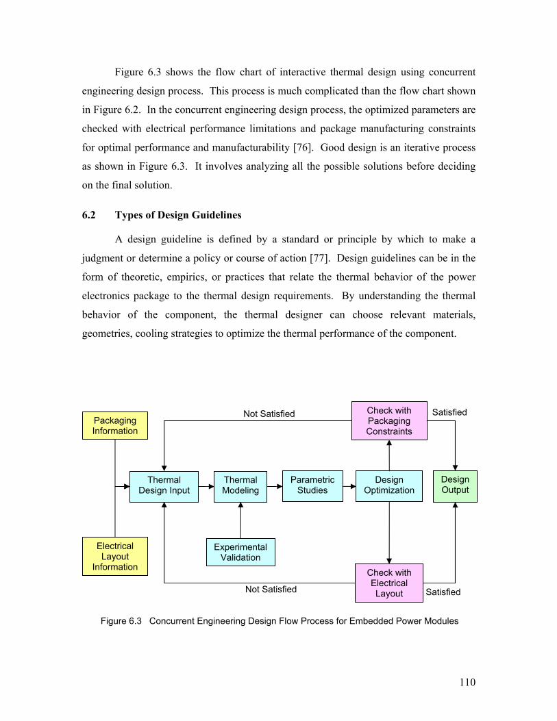
110
Figure 6.3 shows the flow chart of interactive thermal design using concurrent
engineering design process. This process is much complicated than the flow chart shown
in Figure 6.2. In the concurrent engineering design process, the optimized parameters are
checked with electrical performance limitations and package manufacturing constraints
for optimal performance and manufacturability [76]. Good design is an iterative process
as shown in Figure 6.3. It involves analyzing all the possible solutions before deciding
on the final solution.
6.2 Types of Design Guidelines
A design guideline is defined by a standard or principle by which to make a
judgment or determine a policy or course of action [77]. Design guidelines can be in the
form of theoretic, empirics, or practices that relate the thermal behavior of the power
electronics package to the thermal design requirements. By understanding the thermal
behavior of the component, the thermal designer can choose relevant materials,
geometries, cooling strategies to optimize the thermal performance of the component.
Figure 6.3 Concurrent Engineering Design Flow Process for Embedded Power Modules
Experimental Validation
Thermal Modeling
Parametric Studies
Design Output
Thermal Design Input
Design Optimization
Electrical Layout
Information
Packaging Information
Check with Packaging Constraints
Check with Electrical Layout
Not Satisfied Satisfied
Not Satisfied Satisfied

111
The role of the design guidelines is to provide some insight to the design
parameters during the design process. Although the designer may be faced with the
available choices for the design, the main point in using the design guidelines is to
recognize the available information as well as the known constraints. Common thermal
design goals in the power electronic components typically relate to the thermal
performance, reliability, cost, as well as weight and size reduction. Package design
constraints can constitute information on the package manufacturing, assembly, electrical
performance, and environment limitations.
General guidelines are broader theoretical considerations which are not confined
necessarily to a single engineering mechanism. Generally, design guidelines are formal
statements of what have been known or the embedded knowledge implanted in routine
work. According to Dix et al. [78], conceptual guidelines are applicable during early
stage of the design activities and detailed guidelines are applicable during later stage of
the design activities. Conceptual design guidelines gather all the elements of the design
as a whole. The conceptual design is the initial rough design concept. It is an early
process where brainstorming ideas are put into preliminary analysis. On the other hand,
detailed design expands the preliminary design to the extent that the design is sufficiently
implemented. It involves the specification of how an individual component of a system
will function.
Suh [79] presented the axiomatic approach to design in which basic principles
govern decision making in design. The axiomatic approach is a design procedure.
According to Suh [79], there are only two design axioms derived from the generalization
of good design practice that govern good design:
Axiom 1 The Independence Axiom
Axiom 2 The Information Axiom
Axiom 1 states that the design parameters and the functional requirements are related
such that the specific design parameters can be adjusted to satisfy its corresponding
functional requirements without affecting other functional requirements. In addition,
Axiom 2 states that the best design is a functionally uncoupled design that has the
minimum information content.

112
Similarly, corollaries or may be called design rules for design are all derived from
the two basic axioms. These corollaries can be expressed as the following:
Corollary 1 Decoupling of Coupled Design
Corollary 2 Minimization of Functional Requirements
Corollary 3 Integration of Physical Parts
Corollary 4 Use of Standardization
Corollary 5 Use of Symmetry
Corollary 6 Largest Tolerance
Corollary 7 Uncoupled Design with Less Information
While the different design guidelines mentioned are applicable to the thermal design of
the Embedded Power modules, this research work used different design guideline
concepts to achieve a set of thermal design guidelines for the Embedded Power modules.
6.3 Thermal Modeling Guidelines for Embedded Power Modules
While most of the thermal behavior in electronics is complex and three-
dimensional, numerical modeling is often used to mathematically describe and obtain
information on the thermal response of the electronics either in steady state or transient
conditions. Similarly, to understand the thermal behavior of the irregular structure of the
Embedded Power modules as well as its complexity in the heat flow within the modules
is to use numerically modeling method. With commercially available numerical software
such as Flotherm®, Icepack®, I-DEAS ESC, Sinda, and Ansys, one can easily use the
software to model the heat flow within the module.
Although the lead time for learning these software packages differ, their
capabilities do not vary significantly. Therefore, the designer can use whichever software
that he or she is comfortable with. However, the designer should always perform
experimental validation of the thermal models to ensure the accuracy of the software
program in modeling the heat equations as well as the Navier-Stokes equations. There
are three main heat transfer modes; namely, conduction, convection, and radiation. Eq.
6.1 shows the equation for conduction in steady state, mainly named Fourier’s Law of
conduction:

113
tTVCρ)
zT
yT
xT(k p2
2
2
2
2
2
∂∂⋅⋅⋅=
∂∂
+∂∂
+∂∂
⋅ , (6.1)
where k is the thermal conductivity, T is the temperature, x is the x-direction, y is the y-
direction, z is the z-direction in Cartesian coordinate, ρ is the density, Cp is the constant
pressure heat capacitance, V is the volume, and t is the time.
Equation for heat convection, Newton’s second law of cooling, is shown in Eq.
6.2:
)TT(AhQ ∞−⋅⋅= , (6.2)
where Q is the heat dissipation, h is the heat transfer coefficient, A is the convection area,
T is the object temperature, an T∞ is the ambient air temperature. In addition, the heat
transfer through radiation mechanism in electronics cooling is governed by Stefan-
Boltzmann law and can be described by Eq. 6.3:
)TT(AσεQ 4s
4 −⋅⋅⋅= , (6.3)
where Q is the heat dissipation, ε is the emissivity, σ is the Stefan constant (5.67 x 10⁻⁸
W/m2-K4), A is the area, T is the object temperature, and Ts is the surrounding
temperature.
In computational fluid dynamic analysis, Navier-Stokes equations are commonly
used to calculate the fluid flow field. Navier-Stokes equations are the foundation of fluid
mechanics and describe the fluids in motion. For example, the governing equations
solved by I-DEAS ESC are the time-averaged Navier-Stokes equation for three-
dimensional flows. These equations expresses the conservation of mass, conservation of
energy, and conservation of momentum of the fluid flow at all situations.
Thermal simulations can be performed using different methods depending on the
objectives of the study. In most system level thermal modeling for electronic systems,
the understanding of the fluid flow within the electronic enclosure is desired to predict
accurate temperature distribution within the electronic equipment. In this case, a CFD-
based thermal simulation is preferred because it helps analyzing airflow and direction.
Ultimately, the local heat transfer coefficient values can be obtained from the CFD
simulation for predicting the temperature of critical components within electronic

114
equipment. If the heat transfer coefficient values are known, a CFD-based thermal
simulation is not necessary required. Thus, the simulation is simplified to the conduction
problem only. This reduces the finite element model size as well as the computational
time.
This technique can also be applied to module-level thermal analysis with known
equivalent heat transfer coefficients on the surfaces of the module. With the potential
smaller finite element size without CFD analysis, the thermal modeling at module level
can be more detailed. This allows for representing the package in sufficient geometric
detail to capture all relevant thermal paths accurately. In addition, the flexibility in model
changes such as parametric analyses, sensitivity analysis, component placing studies, and
component sizing analyses in the preliminary design allows for shorter computational
time and sensible results.
The accuracy of the input parameters in the model is critical for obtaining
accurate results. A sensitivity analysis is important to study how sensitive the outcomes
are to the changes in the inputs. The sensitivity of a given parameter refers to how
sensitive a given output variable is to changes in that input parameter. It is important to
understand these sensitivities to determine their effects on the design studies conducted
using the numerical simulations.
In identifying sensitive input parameters for the thermal modeling of IPEMs,
critical input parameters and output variables were identified and are summarized in
Table 6.1. The critical input parameters include the interface material thicknesses and the
thermal conductivities of the interface materials. The input parameters are represented by
the equivalent thermal resistance of each interface layer within the model. The critical
output variables are the chip temperatures.
The sensitivity coefficient for an output variable j to an input parameter i was
defined as a dimensionless term, Xij+:
+
+
+
++ ==
Si
j
i
jij
β∆
T∆
δβ
TδX . (6.4)

115
where ∆βSi+ us the dimensionless parameter of the difference of the perturbed parameter
defined in Eq. 6.5:
Ni
NiSi
Ni
SiSi β
βββδβ
β∆−
==+ , (6.5)
where βNi is the nominal parameter value and βSi is the perturbed value. Thus, for a 5%
variation in the nominal parameter value,
05.0β
β05.0β
β)β05.0β(βββ
Ni
Ni
Ni
NiNiNi
Ni
NiSi =⋅
=−+
=− . (6.6)
That is, ∆βSi+ represents a 5% variation in the nominal parameter value, βNi. The non-
dimensional temperature, ∆T+, is defined by:
∞
+
−−
=T)β(T
)β(T)β(TT∆
NiN
SiSNiN , (6.7)
where T∞ is the ambient temperature, and TN(βNi) and TS(βSi) are the respective predicted
temperature for each parameter using βNi and βSi. Note that TN(βNi) is also referred to as
the nominal temperature.
Figure 6.4 shows the result of the sensitivity of the input parameters on the output
variables. The most sensitive input parameter in the model is the thermal conductivity of
the solder material, especially to the temperature of the SiC diode followed by the copper
material. In addition, the temperature of the SiC diode 1 is relatively sensitive to the
thickness of the solder layer between the SiC diode 1 and the DBC trace compared to
other input parameters. Overall, the result shows that the input parameters such as the
thickness and the thermal conductivity of the interface materials are insensitive (Xi+<<1),
thus, indicating that these input parameters do not have significant effect on the results
presented in Chapter 5.
Despite the advances in numerical modeling, any mathematical model is a
simplified model of the reality. Therefore, validation of the numerical model becomes
crucial in determining the exactness of mathematical model. Experimentation is the most
common way of conducting validation on the numerical model. In validating the thermal
model, the simulation results are compared to the experimental data. The validated

116
thermal model can better predict the temperature distribution of the component. Thus, it
can then be used for various thermal design purposes without building the actual
prototype.
In summary, the guidelines for the thermal modeling of Embedded Power
modules can be listed as the following:
− Know the goals of the thermal modeling (e.g. thermal analysis, model
validation, thermal design optimization)
− Understand the geometry and the structure of the Embedded Power modules
including the interfaces
− Collect information on the thermal properties of the materials used in the
Embedded Power modules
− Understand the heat transfer phenomena (conduction, convection, radiation)
within the electronic package and from the package to the environment
− Understand the heat flow path within the package
− Know the boundary conditions (e.g. power loss, interfacial conditions,
environmental condition)
6.4 Thermal Testing Procedure and Guidelines
Thermal testing is widely used for several purposes such as thermal
characterization of electronic components and equipment, validation of numerical
models, as well as thermal study on the electronic components and systems. Thermal
testing usually involves temperature measurements using temperature sensors and
thermography infrared thermometer. Commonly used temperature sensors for
experimentation include thermocouple wires, thermistor, and resistive temperature
devices (RTD). Other method includes diode temperature sensing technique. In
addition, Azar et al. [80] presented liquid crystal imaging for temperature measurement
of electronic devices.

117
Table 6.1 Description and Nominal Values of Parameters Used in Sensitivity Analysis
Sensitivity Parameter, βi
Description of the Represented Thermal Resistance Nominal Value, βNi
Solder 1 (t) Thickness of the Solder Between CoolMOS 1 and DBC Copper Trace 0.53 mm
Solder 2 (t) Thickness of the Solder Between CoolMOS 2 and DBC Copper Trace 0.53 mm
Solder 3 (t) Thickness of the Solder Between SiC 1 and DBC Copper Trace 0..39 mm
Epoxy 1 (t) Thickness of the Epoxy Between CoolMOS 1 and Ceramic Carrier 0.51 mm
Epoxy 2 (t) Thickness of the Epoxy Between CoolMOS 2 and Ceramic Carrier 0.51 mm
Epoxy 3 (t) Thickness of the Epoxy Between SiC 1 and Ceramic Carrier 0.51 mm
Polyimide_Top (t) Thickness of the Top Polyimde 0.127 mm
Polyimide_Bottom (t) Thickness of the Bottom Polyimde 0.127 mm
Copper (k) Thermal Conductivity of Copper 395 W/m-K
Alumina (k) Thermal Conductivity of Alumina 26 W/m-K
Aluminum Nitride (k) Thermal Conductivity of Aluminum Nitride 180 W/m-K
Silicon (k) Thermal Conductivity of Silicon 117 W/m-K
Silicon Carbide (k) Thermal Conductivity of Silicon Carbide 490 W/m-K
Gel (k) Thermal Conductivity of Gel 0.2 W/m-K
Solder (k) Thermal Conductivity of Solder 51 W/m-K
Polyimide (k) Thermal Conductivity of Polyimide 0.3 W/m-K
Epoxy (k) Thermal Conductivity of Epoxy 1.4 W/m-K
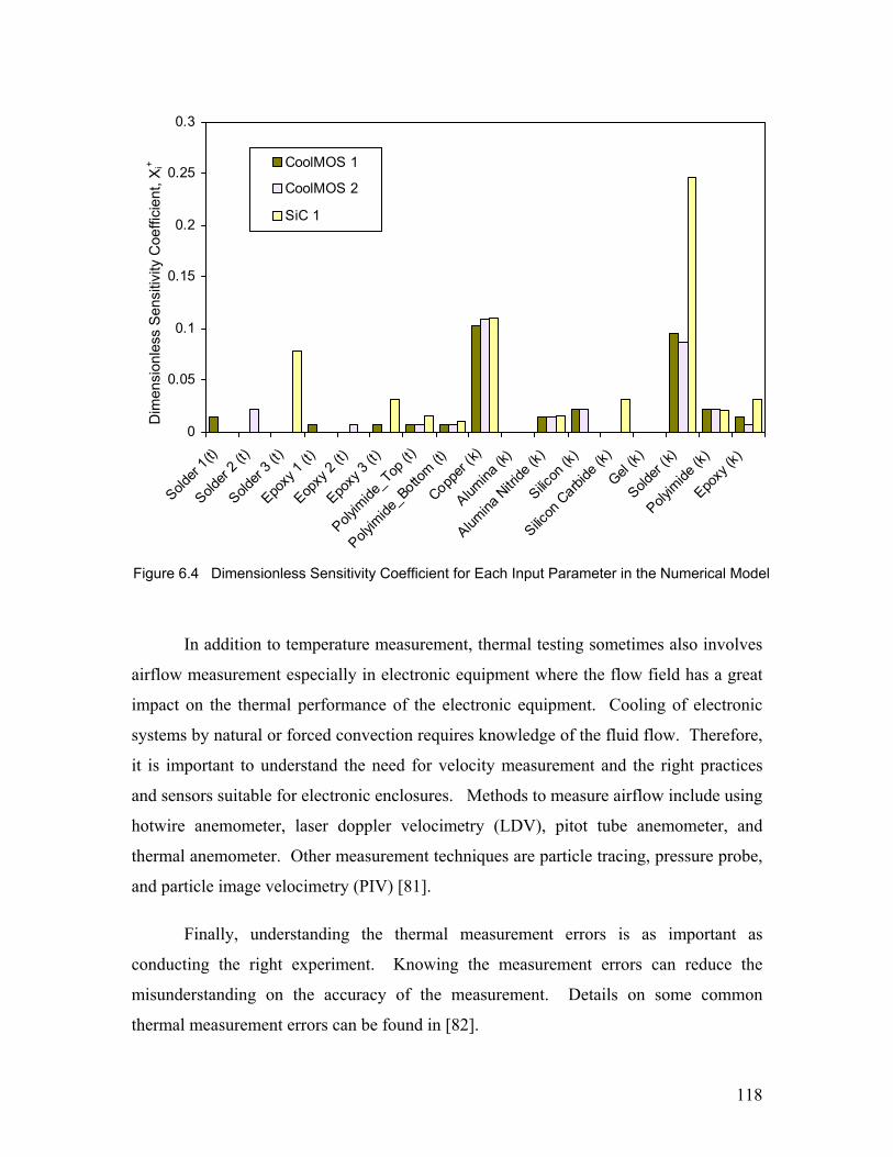
118
Figure 6.4 Dimensionless Sensitivity Coefficient for Each Input Parameter in the Numerical Model
In addition to temperature measurement, thermal testing sometimes also involves
airflow measurement especially in electronic equipment where the flow field has a great
impact on the thermal performance of the electronic equipment. Cooling of electronic
systems by natural or forced convection requires knowledge of the fluid flow. Therefore,
it is important to understand the need for velocity measurement and the right practices
and sensors suitable for electronic enclosures. Methods to measure airflow include using
hotwire anemometer, laser doppler velocimetry (LDV), pitot tube anemometer, and
thermal anemometer. Other measurement techniques are particle tracing, pressure probe,
and particle image velocimetry (PIV) [81].
Finally, understanding the thermal measurement errors is as important as
conducting the right experiment. Knowing the measurement errors can reduce the
misunderstanding on the accuracy of the measurement. Details on some common
thermal measurement errors can be found in [82].
Dim
ensi
onle
ss S
ensi
tivity
Coe
ffici
ent,
X i+
0
0.05
0.1
0.15
0.2
0.25
0.3
Solder
1(t)
Solder
2 (t)
Solder
3 (t)
Epoxy
1 (t)
Eopxy
2 (t)
Epoxy
3 (t)
Polyim
ide_Top
(t)
Polyim
ide_Botto
m (t)
Copper
(k)
Alumina
(k)
Alumina
Nitri
de (k
)
Silicon
(k)
Silicon
Carbi
de (k
)
Gel (k)
Solder
(k)
Polyim
ide (k
)
Epoxy
(k)
CoolMOS 1
CoolMOS 2
SiC 1

119
In summary, the guidelines for the thermal testing of Embedded Power modules
can be summarized as the following:
− Understand the objectives of the thermal testing
− Know the environment you test the module (flow velocity, fan speed, size of
the enclosure, ambient temperature)
− Use the right type of sensors for your measurement
− Employ optimum sensor placement strategies (best place to place the
sensors for minimum noise, methods of attaching sensors)
6.5 Thermal Design Guidelines for Embedded Power Modules
The purpose of the design guidelines is to provide more suggestive and general
rules in determining and predicting the thermal performance of the Embedded Power
modules. Although the guidelines documented here are more towards abstract (principle)
guidelines, some detailed guidelines will also be discussed.
The thermal design of the Embedded Power modules was based on simplicity,
efficiency, and reliability where these three functional restraints were defined in “solution
neutral” environment. Trade-offs in different ceramic materials, chip-to-chip distances,
copper trace areas, dielectric material thicknesses, metallization thicknesses,
metallization materials, and metallization interconnect patterns were considered with
respect to the electrical performance limitations and the package manufacturing
limitations.
In summary, the guidelines for the thermal design of Embedded Power modules
can be summarized as the following.
I. Ceramic Material Selection
In Embedded Power modules, there are two layers where ceramic substrates are
used for electrical insulation. These layers are also aimed to function as good thermal
path for conducting the heat from the power chips to the outer surface of the package.
One of these layers is the DBC ceramic layer while the other one is the ceramic carrier
layer. The heat conduction through these layers is proportional to the thermal

120
conductivity of the layer but inversely proportional to the thickness of the ceramic layer
as expressed in Eq. 6.8:
cer
cercercer RT∆
tT∆AkQ == , (6.8)
where Qcer is the heat transfer through the ceramic layer, kcer is the thermal conductivity
of the ceramic, A is the area of the ceramic, ∆T is the temperature difference between the
two conducting surface of the ceramic, t is the thickness of the ceramic layer, and Rcer is
the thermal resistance of the ceramic layer. Therefore, in selecting the ceramic material
from the thermal perspective, the higher thermal conductivity of the ceramic material
with the smallest thickness can yield good heat transfer through the ceramic layers.
It was also found in this research that the ceramic carrier has less impact on the
overall temperature of the module since most of the heat is transported through the solder
layer to the DBC. Therefore, having low thermal resistance on the DBC layer can help
improve the thermal performance of the module. While DBC substrate is commonly
used in power electronic packaging, new materials with a lower thermal resistance than
the DBC substrate can be good candidates for its replacement.
II. Chip Placement
Each power chip is soldered to the DBC copper trace in the Embedded Power
modules. The distance between the chips does not have significant influence on the chips
temperatures. This is because the major heat path from the chip is through the solder
layer and to the individual DBC copper trace layer. From there, the heat is conducted
through the DBC ceramic layer and the DBC bottom copper layer. Therefore, the mutual
effect of the two chips on different copper trace is small.
If more than one chip is sharing the same DBC copper trace, the mutual effect
between the chips is still insignificant due to the thin layer of the copper trace and the
minimal heat spreading within the copper trace layer. As a result, the distance between
the chips will be determined by the packaging constraint. Overall, the distance between
the chips is not a major factor influencing the thermal performance of the module since
the heat flow from the power chips is mostly confined by the thinness of the DBC layers
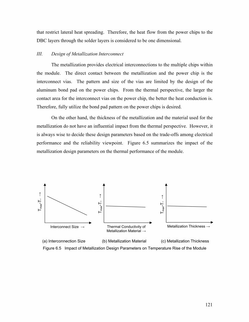
121
that restrict lateral heat spreading. Therefore, the heat flow from the power chips to the
DBC layers through the solder layers is considered to be one dimensional.
III. Design of Metallization Interconnect
The metallization provides electrical interconnections to the multiple chips within
the module. The direct contact between the metallization and the power chip is the
interconnect vias. The pattern and size of the vias are limited by the design of the
aluminum bond pad on the power chips. From the thermal perspective, the larger the
contact area for the interconnect vias on the power chip, the better the heat conduction is.
Therefore, fully utilize the bond pad pattern on the power chips is desired.
On the other hand, the thickness of the metallization and the material used for the
metallization do not have an influential impact from the thermal perspective. However, it
is always wise to decide these design parameters based on the trade-offs among electrical
performance and the reliability viewpoint. Figure 6.5 summarizes the impact of the
metallization design parameters on the thermal performance of the module.
(a) Interconnection Size (b) Metallization Material (c) Metallization Thickness
Figure 6.5 Impact of Metallization Design Parameters on Temperature Rise of the Module
Interconnect Size →
T max
-T∞
→
Thermal Conductivity of Metallization Material →
T max
-T∞
→
Metallization Thickness →
T max
-T∞
→

122
IV. Thermal Management for Embedded Power Modules
The studies in this research have shown that the most effective way of reducing
the maximum temperature of the module is to have effective heat dissipation strategies
from the package to the environment. While most of the heat is transported through the
soldered side of the power chips, heat extraction through the top side of the power chips
is also desired. Metallization is the structure that has direct contact with the power chips
from the top. However, the very thin layer of metallization does not help in spreading
heat over the layer but results in hotspots.
To further extract the heat from these hotspots, localized cooling is desired. This
can be achieved through both active and passive cooling strategies. Mechanically
assisted cooling systems are said to provide active cooling since they require energy.
Active cooling includes refrigeration and thermo-electric cooling. Passive cooling
strategies are widely used in electronic cooling. Typical passive cooling techniques
apply high thermal conductivity adhesives, silicone gel, and epoxy to replace low thermal
conductivity interface materials. Other cooling strategies include liquid cooling, spray
cooling, and heat pipes.
Reducing the package thermal resistance, Rj-c, shall be one of the goals of the
thermal design for the Embedded Power modules. Though it has shown that the most
influential parameter in reducing the maximum temperature of the module is the external
thermal resistance, Rc-a, any design effort in reducing the Rj-c is valuable. A further effort
should extend to enhance the thermal design of the module such that the heat from the
package can be carried away to the ambient easily. Consequently, this requires a low Rc-a
and thus desires effective mechanisms to transfer the heat from the package to the
ambient. Several different strategies such as double-sided cooling can be employed to
achieve low Rc-a as shown in the previous chapter.
6.6 Summary
In summary, there is no one unique design path to follow in the thermal design of
Embedded Power modules. The designer should consider multiple design options before
deciding the final design that best prescribed the objective of the design. The thermal

123
design steps are iterative with the input from and output to the electrical designer and the
packaging engineer. Common design parameters for the Embedded Power modules are
materials, interfaces, and geometric configurations. The role of the thermal designer is to
select the most compatible design parameters with trade-offs among the design goals and
constraints. Finally, as a thermal designer, you have to think logically, avoid technical
conceit, and avoid disguised assumptions.

124
Chapter 7 Conclusions
Growing dependence on power electrics has caused an urge in the need for high
reliability power electronics to convert raw forms of electric power to different forms for
individual applications. The demands on performance, cost, and reliability have
drastically influenced the packaging and interconnection technologies in this field. New
packaging and interconnection technologies are desired to handle multiple chips with
high power density packaged in a smaller volume. With ever-rising heat fluxes in
continuously miniaturized power electronics, the understanding of heat transfer
phenomena in power electronics is becoming crucial to the design, providing proper
thermal management for high reliability.
The trend toward higher power density requires a greater attention to heat
transfer. The primary goal in thermal design is to limit the junction temperature of the
power electronics modules. With the lack of knowledge of the impact of the new
packaging technology on the thermal performance of the module, a good understanding
of the thermal behavior of the module can help in both identifying potential thermal
failure and designing appropriate thermal management strategies for the module.
Simulation tools and experimentation are commonly used to perform the thermal
analysis. Advanced thermal management such as forced air cooling, liquid cooling, and
heat pipes are extensively used to improve the thermal performance of electronic
components and equipment. Consequently, substantially higher thermal conductivity
materials will also aid in adequately dissipating heat loads from high heat flux power
chips.
In this research, we performed a thorough thermal analysis and achieved an in
depth understanding of the thermal behavior of Embedded Power modules. We also
accomplished several goals discussed in Chapter 1. The summary and contributions of
this research are discussed in the following.

125
7.1 Contributions
I. Understanding of the thermal behavior and heat transfer in Embedded Power
modules
a. The studies have shown that the hotspots in the module are the power chips, as one
might expect. Heat flow from the power chips through the bottom side and the top
side are considered virtually one dimensional. The heat from the power chip is barely
conducted laterally to the ceramic carrier due to the low thermal conductivity of the
interfacial material—epoxy.
b. This research has found that the position of the chips within the module and the size
of the power chips can result in different junction-to-ambient thermal resistance, Rj-a,
for the chips. The chip temperature rise maintained a linear relationship with the
power loss although the chips were packaged using Embedded Power technology.
The results were also useful to determine the allowable power loss for the module
under variable ambient temperature with an air velocity of 2.2 m/s.
c. The methodology for obtaining the thermal resistance matrix to describe the thermal
resistance of a multi-chip module was demonstrated. The prediction errors using the
resistance matrix were examined against numerical results. This study has shown that
the resistance matrix can predict the temperature of the individual chip in a multi-chip
module within an acceptable error margin of 5% to 10% in the heat dissipation range
of 10 W to 30 W.
d. Overall, the studies in this research have demonstrated the use of two different
methods (numerical and experimental) in obtaining information on the thermal
behavior of the Embedded Power module. The studies discussed in previous chapters
have also shown how and where these two different methods can be used to acquire
necessary information on the thermal performance or the thermal behavior of the
module.

126
II. Understanding of the effect of the material properties and geometrical sizing of
specific structure on the thermal performance and the stress distribution of
planar multi-layer structures
a. The DBC ceramic dominates the ceramic carrier in transferring the heat away from
the power chips. While a ceramic substrate is commonly used in the packaging of the
Embedded Power modules, a high thermal conductivity value ceramic substrate can
substantially help in improving the heat transfer within the module. Common
ceramic materials are alumina and aluminum nitride. The thermal conductivity of
aluminum nitride is about six times higher than alumina although aluminum nitride is
much more expensive than alumina. The study has shown that replacing the alumina
ceramic carrier with aluminum nitride or ALOX™ substrate can reduce the maximum
temperature rise of the module by 3%. Further improvement of 9% can be achieved
by replacing the alumina DBC substrate with aluminum nitride.
b. The temperature rise of the module can be reduced as much as 5% with an optimized
polyimide thickness. Investigation on the thickness of the polyimide layer was
performed to further understand the task of polyimide layer in effectively transporting
the heat within the heat path in the module.
c. The distance between the two MOSFET chips is not an important parameter in the
thermal design. Studies on the effect of the chip-to-chip distance and copper trace
area on the thermal performance of the DC/DC IPEM using simplified models were
presented. The placement of the MOSFET should be considered from other factors
such as the length of the electrical interconnects as well as the overall layout
constraints. In addition, the size of the copper trace area should also be determined
based on the best electrical performance as well as the overall layout constraints.
d. The metallization contact area, type, and thickness have relatively small influence on
the chip temperature compared to von Mises stress. The study on the design
parameters of the metallization layer provides some insight on the effect of different
interconnect patterns, metallization thicknesses, and metallization materials on the
thermal and thermomechanical performances of the Embedded Power modules using

127
metallization bonding as the interconnect method. Key findings from this preliminary
study include:
− Temperature rise of the module is directly related to the total contact surface
area of the interconnect pattern. On the other hand, the von Mises stress
depends on the interconnect pattern rather than the total contact surface area.
The study had shown that using 6 holes and 9 holes interconnect patterns
yielded the same maximum von Mises stress since the interconnect patterns for
both cases were round. Instead, replacing the round pattern with large
continuous surface such as rectangular pattern would reduce the stress on the
silicon die. However, the improvement obtained in the stress reduction in the
metallization was greater than the increase in the stress on the silicon die (6.4%
vs. 3.5%).
− Increasing the metallization thickness slightly improved the thermal
performance of the module. On the other hand, considerable increase in stress
was observed by increasing the metallization thickness more than 16x of the
baseline thickness on the metallization.
− The matching of CTE dominates the effect of the thermal conductivity of the
material in selecting a better material for the metallization. Of all the materials
investigated in this study, molybdenum is the most suitable material when
considering the trade-offs between the thermal and thermomechanical
performance.
− The von Mises stress distributions and the maximum average von Mises stress
on both the silicon and the metallization do not vary significantly (within 5%)
in comparing four different sets of restraints defined in the stress model.
III. Development of detailed numerical modeling techniques for planar multi-layer
structures
a. A modeling methodology was developed for integrated power electronics modules.
An approach to assess the needed accuracy level in thermal analysis of integrated
power electronics modules is presented to aid in efficient and timely heat transfer
analysis. The methodology could also be applied to any complex electronic package

128
in general. The module conduction is modeled in great detail accounting for the
different materials and geometric complexities.
b. Numerical models of the IPEMs were developed using a commercial finite element
program, I-DEAS. Thermal simulations were performed using computational fluid
dynamics code in I-DEAS, ESC, to identify hotspots as well as to predict steady-state
temperature distributions within the modules. The detailed modeling of the heat
transfer phenomena in the IPEMs is very challenging due to the complexness of the
geometry, the unknown interface conditions within the module a priori, and the
unverified material properties. This research also demonstrated a methodology for
validating numerical model with experimental data. The exact experiment
environment was modeled and the results show that the numerical model can predict
the temperature of the IPEMs with about 5% difference of experimental data.
c. Different ways of defining constraints on the stress models were explored. This study
particularly investigated four different constraint sets to understand the sensitivity of
the simulation results on different constraints. The results showed that both the von
Mises stress and stress distribution are not influenced by different constraints studied
here.
IV. Introduction of new integrated cooling strategies for planar multi-layer
structures
a. The study shows that structural enhancement can reduce the maximum temperature
of the module by as much as 24%. Studies in this research have shown that simple
modifications on the geometry or the material can significantly improve the thermal
performance of the IPEMs. Finding ways to create direct heat paths from the heat
sources proves to be an effective method to improve the thermal performance of the
module.
b. Improvement ranging from 30% to 60% can be observed with the implementation of
double-sided cooling and further improvement can be achieved through micro-
channel cooling. By soldering additional DBC on the top side of the module enables
the employment of double-sided cooling for the module. This opens up various
129
cooling strategies that can be used for different applications such as single and two
phase forced air and liquid cooling. To reduce the internal thermal resistance of the
module, several combinations of the ceramic materials were studied. The use of DBC
and Thermal Clad™ were also compared but the use of DBC proved to be better than
Thermal Clad™. Similarly, preliminary study on integrating micro-channel cooling
into the structure of the module also shows great improvement on the thermal
performance of the module. While a specific structure was used as the case study in
this study, the discussed methods of improving the thermal performance of module
are applicable to general Embedded Power packages.
V. Development of thermal design rules for planar multi-layer structures
The purpose of developing thermal design rules is to suggest some guiding
principles that are behind most thermal designs in Embedded Power modules and help
future design and development of the Embedded Power modules. Very often in the
process of the new design of similar product, designers have to learn by making mistakes.
Possibly they will have to repeat the same type of mistakes as the previous designers
before they realize what went wrong. Therefore, this research seeks to provide some
guidelines to avoid such mistakes as well as replication of similar analyses in the future.
a. A few guidelines were developed to perform thermal analysis of Embedded Power
modules using commercial software. Thermal analysis using commercial numerical
modeling tool has become popular approach for analyzing the heat transfer in
electronics. Simulation is a power tool for the analysis of new product designs.
Thus, simulations are widely used for predicting the performance of a system,
identifying potential thermal problems, verifying a design, and evaluating possible
solutions to the problems. To achieve successful simulation studies, the user needs to
understand the capability of the software as well as the shortcoming of the software.
b. A thermal testing procedure and guideline for Embedded Power modules was
outlined. Experiments are often conducted to evaluate, compare, and provide insight
into the design. In addition, experimentation can also validate numerical models.
Validation is an essential phase in the numerical model development process for any
simulation to avoid major and serious modeling errors. Consequently, any mistake in

130
performing the experiments or taking the measurements will lead to inaccurate
information and design.
c. A thermal design guideline for the Embedded Power modules was outlined. These
guidelines include ceramic material selection, chip placement, design of the
metallization interconnect, and thermal management for the Embedded Power
modules.
7.2 Recommendations
Detailed Models. In general, all power losses in switch mode power electronics consist
of switching loss and conduction loss. These losses are calculated based on the switching
waveforms of the voltage and current for switching loss and resistances of resistive
elements in the circuit for conduction loss. The current thermal models used in this
dissertation are for steady-state conditions. These models assume that the power loss
from the power chip was constant as an average loss over time and uniformly distributed
on the top surface of the power chips. Although it was demonstrated that these
assumptions is feasible and can be greatly validated by experimental results, future
thermal models should include the capability of using the waveform of the power loss
over time as the boundary conditions and perform transient analysis in detail. In addition,
a detailed distribution of the power loss on the power chips is desired for further
identifying the hotspots on the chips.
New Materials. The selection of the packaging materials is important in achieving
improved performance electrically and thermally as well as reliability. Although the
current materials used in the Embedded Power modules are commercially available, the
selection of the packaging materials should continue to search for emerging packaging
materials that may provide promising improved performance. In particular, high thermal
conductivity solder, power chips materials, insulation materials such as polyimide, and
ceramic substrates are always appreciated in achieving better thermal performance for the
module.
New Cooling Technologies. The studies in this dissertation show that the external heat
extraction from the module to the ambient is more significant than the passive thermal

131
management strategies (such as the rearrangement of the chips) within the module.
Although this research has demonstrated the possible implementation of integrated
cooling strategies and its advantages, future investigations should include implementing
these strategies into power electronics systems testbeds. In addition, future work should
also focus on developing new cooling strategies (such as liquid cooling, two-phase
cooling, spray cooling) that can be integrated structurally into he Embedded Power
modules.
Design Rules. This dissertation outlines some guidelines for the thermal design of the
Embedded Power modules. While these guidelines are applicable to the future thermal
design of any multi-chip modules, specific design rules are also desired for the future
design of the module. Since the best design for the Embedded Power modules is done by
a team that is expert in multidisciplinary area, both mechanical and electrical engineering,
future effort should focus on developing specific rules to provide back-of envelope
calculations with known error margin.

132
Bibliography
[1]. Intel Pentium 4 Processor in the 478-Pin Package Thermal Design Guidelines
(Santa Clara: Intel Corporation, 2002) http://developer.intel.com/design/pentium4/guides/24988903.pdf
[2]. Intel Corporation, “Expanding Moore’s Law—Raising the Bar,” http://www.intel.com/labs/eml/.
[3]. R. Mahajan, R. Nair, V. Wakharkar, J. Swan, J. Tang, and G. Vandentop, “Emerging Direction for Packaging Technologies,” Intel Technology Journal, Volume 6, Issue 2, May 2002, pp. 62-75.
[4]. Heat Density Trends in Data Processing, Computer Systems and Telecommunication Equipment (Santa Fe: The Uptime Institute, 2001) http://www.upsite.com/TUIpages/whitepapers/tuiheat1.0.html.
[5]. B. A. Myers, “Cooling Issues for Automotive Electronics,” ElectronicsCooling, August 2003, pp. 24-27.
[6]. Data Points, “Electronic Motor Drive Market Projected to Top $19 Billion by 2005,” Power Electronics Technology Magazine, September, 2001, pp. 10.
[7]. S. Mulgaonker, B. Chambers, and M. Mahalingam, “An Assessment of the Thermal Performance of the PBGA Family,” IEEE Transactions on Components, Packaging, and Manufacturing Technology-Part A, Vol. 18, No. 4, December 1995, pp. 739-748.
[8]. M. Mita, T. Kumakura, S. Inoue, and Y. Hiraki, “Advanced TAB/BGA Multi-Chip Staked Module for High Density LSI Packages,” Proceedings of Multi-Chip Module Conference, 1994, pp. 68-76.
[9]. T. D. Yuan, “Thermal Performance Characteristics Comparison Between Flip-chip and Wirebond Ceramic Multichip Modules,” Proceeding of Multi-Chip Module Conference, 1996, pp.44-48.
[10]. Y. G. Kim, “Folded Staked Package Development,” Proceedings of 52nd Electronic Components and Technology Conference, 2002, pp. 1341-1346.
[11]. J. W. Balde, Foldable Flex and Thinned Silicon Multichip Packaging Technology, 1st Edition (Massacuhusetts: Kluwer Academic Publishers, 2003), pp. 1-14.
[12]. J. U. Meyer, M. Schuettler, O. Scholz, W. Haberer, and T. Stieglitz, “Flexible, Microarray Interconnection Technique Applied to Biomedical Microdevices,” Foldable Flex and Thinned Silicon Multichip Packaging Technology, 1st Edition (Massacuhusetts: Kluwer Academic Publishers, 2003), Chapter 6, pp. 154-158.

133
[13]. X. Fan and S. Haque, “Emerging MOSFET Packaging Technologies and Their Thermal Evaluation,” Proceedings of 8th Inter-society Conference on Thermal Phenomena in Electronic Systems (I-THERM), 2002, pp. 1102-1108.
[14]. B. Ozmat, “Interconnect Technologies and the Thermal Performance of MCM,” IEEE Transaction on Components, Hybrids, and Manufacturing Technology, Vol. 15, No. 5, October 1992, pp. 860-869.
[15]. K. Sienski, R. Eden, and D. Schaefer, “3-D Electronic Interconnect Packaging,” Proceedings of Aerospace Applications Conference, Vol. 1, 1996, pp. 363-373.
[16]. B. Ozmat, V. A. K. Temple, and J. K. Azotea, “An Advanced Packaging Technology for High Performance Power Devices,” Proceedings of the 32nd Intersociety Energy Conversion Engineering Conference, Vol. 1, 1997, pp. 687-693.
[17]. R. Fisher, R. Fillion, J. Burgess, and W. Hennessy, “High Frequency, Low Cost, Power Packaging Using Thin Film Power Overlay Technology,” Proceedings of 10th Applied Power Electronics Conference & Exposition (APEC), Vol. 1, 1995, pp. 12-17.
[18]. T. Stockmeier and W. Tursky, “Present and Future of Power Electronics Modules,” Proceedings of Center for Power Electronics Systems (CPES) Seminar, 2000, pp. 3-9.
[19]. Fuji Semiconductor, Inc., “Power Module IPM,” http://www.fujielectric.co.jp/eng/denshi/scd/prod_pm.html (Saddle Brook, NJ: Fuji Semiconductor, Inc.)
[20]. Eupec Inc., “Econopack+ ― A New IGBT Module for Optimized Inverter Solutions,” http://www.eupec.com/p/e/pdf/ed_pcim_2000_bostonf.pdf (Nurembug, Germany: Eupec, Inc.)
[21]. Toshiba America Electronic Components, Inc., “Six-In-One Package Offers Low-Cost IGBT Solution for Industrial Drive Market,” http://www.toshiba.com/taec/press/to-717.htm (Irvine, CA: TAEC, 1997)
[22]. A. B. Lostetter, F. Barlow, and A. Elshabini, “An Overview to Integrated Power Module Design for High Power Electronics Packaging,” Journal of Microelectronics Reliability, Vol. 40, Issue 3, March 2000, pp. 365-379.
[23]. Z. Liang and F. C. Lee, “Embedded Power Technology for IPEMs Packaging Applications,” Proceedings of 16th Applied Power Electronics Conference and Exposition (APEC), Vol. 2, 2001, pp. 1057-1061.
[24]. Z. Liang and J. D. van Wyk, “Planar Metallization Interconnected 3D Multi-chip Module,” Proceedings of 53rd Electronic Components and Technology Conference (ECTC), 2003, pp. 1090-1094.

134
[25]. Z. X. Liang, J. D. van Wyk, F. C. Lee, D. Boroyevich, E. P. Scott, J. Chen, and Y. Pang, “Integrated Packaging of a 1 kW Switching Module Using a Novel Planar Interconnect Technology,” IEEE Transactions on Power Electronics, Vol. 19, Issue 1, 2004, pp. 242-250.
[26]. G. L. Ginsberg and D. P. Schnorr, Multichip Modules & Related Technologies, 1st Edition (New York: McGraw-Hill, Inc., 1994), pp. 1-229.
[27]. A. Bergles, “Evolution of Cooling Technology for Electrical, Electronic, and Microelectronic Equipment,” IEEE Transactions on Components and Packaging Technologies, Vol. 26, No. 1, March 2003, pp. 6-15.
[28]. D. Price, “A Review of Selected Thermal Management Solutions for Military Electronic Systems,” IEEE Transactions on Components and Packaging Technologies, Vol. 26, No. 1, March 2003, pp. 26-39.
[29]. K Azar, “Advanced Cooling Concepts and Their Challenges,” Presentation at Therminic 2002.
[30]. C. D. Patel, “Backside Cooling Solution for High Power Flip Chip Multi-chip Modules,” Proceedings of Electronic Components and Technology Conference (ECTC), 1994, pp. 442-449.
[31]. T. Y. Lee, “An Investigation of Thermal Enhancement on Flip Chip Plastic BGA Packages Using CFD Tool,” IEEE Transactions on Components and Packaging Technologies, Vol. 23, No. 3, September 2000, pp. 481-489.
[32]. L. Liang, J. D. Wilson, N. Brathwaite, L. E. Mosley, and D. Love, “High-Performance VLSI Through Package-Level Interconnects,” Proceedings of 39th Electronic Components Conference, 1989, pp. 518-523.
[33]. M. S. Pittler, D. M. Powers, and D. L. Schnabel, “System Development and Technology Aspects of the IBM 3081 Processor Complex,” IBM Journal of Research and Development, Vol. 26, No. 1, January 1982, pp. 2-11.
[34]. R. C. Chu, U. P. Hwang, and R. E. Simons, “Conduction Cooling for an LSI Package: A One-Dimensional Approach,” IBM Journal of Research and Development, Vol. 26, No. 1, January 1982, pp. 45-54.
[35]. A. J. Blodgett and D. R. Barbour, “Thermal Conduction Module: A High-Performance Multilayer Ceramic Package,” IBM Journal of Research and Development, Vol. 26, No. 1, January 1982, pp. 30-36.
[36]. S. Oktay and H. C. Kammerer, “A Conduction-Cooled Module for High-Performance LSI Devices,” IBM Journal of Research and Development, Vol. 26, No. 1, January 1982, pp. 55-66.
135
[37]. I. Mudawar, “Assessment of High-Heat-Flux Thermal Management Schemes,” IEEE Transactions on Components and Packaging Technologies, Vol. 24, No. 2, June 2001, pp. 122-141.
[38]. T. Y. Lee, V. Hause, and M. Mahalingam, “Liquid Encapsulated MCM Package —Thermal Demonstration,” Proceedings of 5th Inter-society Conference on Thermal and Thermomechanical Phenomena in Electronic Systems (ITHERM), 1996, pp. 258-265.
[39]. X. Y. Chen, K. C. Toh, T. N. Wong, J. C. Chai, D. Pinjala, O. K. Navas, Ganesh, H. Zhang, and V. Kripesh, “Direct Liquid Cooling of a Stacked MCM,” Proceedings of 9th Inter-society Conference on Thermal and Thermomechanical Phenomena in Electronic Systems (ITHERM), 2004, pp. 199-206.
[40]. M. C. Shaw, J. R. Waldrop, S. Chandrasekaram, B. Kagalwala, and X. Jing, “Enhanced Thermal Management by Direct Water Spray of High-Voltage, High Power Devices,” Proceedings of 8th Inter-society Conference on Thermal and Thermomechanical Phenomena in Electronic Systems (ITHERM), 2002, pp. 1007-1014.
[41]. W. R. Stubstad, “The Application of Thermoelectric Spot Cooling to Electronic Equipment,” IRE Transaction on Product Engineering and Production, Vol. 5, Issue 4, December 1961, pp. 22-29.
[42]. J. P. Fleurial, A. Borshchevsky, M. A. Ryan, W. Phillips, E. Kolawa, T. Kacisch, and R. Ewell, “Thermoelectric Microcoolers for Thermal Management Applications,” Proceedings of the XVI International Conference on Thermoelectrics, 1997, pp. 641-645.
[43]. R. E. Simons and R. C. Chu, “Application of Thermoelectric Cooling to Electronic Equipment: A Review and Analysis,” Proceedings of 16th IEEE Semiconductor Thermal Measurement and Management Symposium, 2000, pp. 1-9.
[44]. G. L. Solbrekken, K. Yazawa, and A. Bar-Cohen, “Thermal Management of Portable Electronic Equipment Using Thermoelectric Energy Conversion,” Proceedings of 9th Inter-society Conference on Thermal and Thermomechanical Phenomena in Electronic Systems (ITHERM), Vol. 1 pp. 276-283.
[45]. C. Zweben, “Advanced Composites and Other Advanced Materials for Electronic Packaging Thermal Management,” Proceedings of International Symposium on Advanced Packaging Materials: Processes, Properties and Interfaces, 2001, pp. 360-365.
[46]. S. Jha, “CUVAR—A New Controlled Expansion, High Conductivity Material for Electronic Thermal Management,” Proceedings of 45th Electronic Components and Technology Conference (ECTC), 1995, pp. 542-547.

136
[47]. H. L. Davidson, N. J. Colella, J. A. Kerns, and D. Makowiecki, “Copper-Diamond Composite Substrates fro Electronic Components,” Proceedings of 45th Electronic Components and Technology Conference (ECTC), 1995, pp. 538-541.
[48]. G. Ellison, Thermal Computations for Electronic Equipment, (New York: Van Nostrand Reinhold Company, 1984).
[49]. J. C. Eid, “Thermal Modeling with PC Spreadsheets,” Proceedings of 4th Semiconductor Thermal and Temperature Measurement Symposium (SEMI-THERM), 1988, pp. 40-49.
[50]. T. W. C. Mak and L. G. Feinstein, “A Simplified Modeling Technique for Finite Element Thermal Analysis of a Plastic SOIC Package,” IEEE Transaction on Components and Packaging Technologies, Vol. 22, Issue 1, March 1999, pp. 6-10.
[51]. B. A. Zahn, “Evaluating Thermal Characterization Accuracy Using CFD Codes—A Package Level Benchmark Study of IcePak™ and Flotherm®,” Proceedings of 6th Inter-society Conference on Thermal and Thermomechanical Phenomena in Electronic Systems (I-THERM), 1998, pp. 322-329.
[52]. Y. Joshi, M. Baelmans, D. Copeland, C. J. M. Lasance, J. Parry, and J. Rantala, “Challenges in Thermal Modeling of Electronics at the System Level: Summary of Panel Held at the Therminic 2000,” Microelectronics Journal, Vol. 32, Issues 10-11, October-November 2001, pp/ 797-800.
[53]. V. Eveloy, P. Rodgers, and M. S. J. Hashmi, “Numerical Prediction of Electronic Component Operational Temperature: A Perspective,” IEEE Transaction on Components and Packaging Technologies, Vol. 27, No. 2, June 2004, pp. 268-282.
[54]. K. Azar, “Electronic Cooling and the Need for Experimentation,” Thermal Measurements in Electronic Cooling (New York: CRC Press, 1997), pp. 1-43.
[55]. G. B. Kromann, “Thermal Management for Ceramic Multichip Modules: Experimental Program,” Proceedings of Multi-Chip Module Conference (MCMC), 1992, pp. 75-58.
[56]. P. Rodgers, V. Eveloy, J. Lohan, C. M. Fager, P. Tiilikka, and J. Rantala, “Experimental Validation of Numerical Heat Transfer Predictions for Single and Multi-component Printed Circuit Boards in Natural Convection Environments,” Proceedings of 15th Semiconductor Thermal Measurement and Management Symposium (SEMI-THERM), 1999, pp. 54-64.
[57]. J. Lohan, P. Rodgers, C. M. Fager, R. Lehtiniermi, V. Eveloy, P. Tiilikka, and J. Rantala, “Validation and Application of Different Experimental Techniques to Measure Electronic Component Operating Junction Temperature,” IEEE

137
Transactions on Components and Packaging Technology, Vol. 22, No. 2, June 1999, pp. 252-258.
[58]. T. Gautier, “Construction and Validation of Thermal Models of Packages,” Proceedings of 7th Semiconductor Thermal Measurement and Management Symposium (SEMI-THERM), 1991, pp. 74-79.
[59]. JEDEC Standard, http://www.jedec.org.
[60]. R. Moffat, “Uncertainty Analysis,” Thermal Measurements in Electronic Cooling (New York: CRC Press, 1997), pp. 46-80.
[61]. B. S. Lall, B. M. Guenin, and R. J. Molnar, “Methodology for Thermal Evaluation of Multichip Modules,” Proceedings of 11th Semiconductor Thermal Measurement and Management Symposium (SEMI-THERM), 1995, pp. 72-79.
[62]. J. W. Sofia, “Fundamentals of Thermal Resistance Measurement,” 1995, http://www.analysistech.com/PDF_Files/fundamen.pdf.
[63]. L. Liang and A. Hamzehdoost, “Guidelines for Thermal Management of Multichip Modules,” Proceedings of 42nd Electronics Components and Technology Conference, 1992, pp. 787-791.
[64]. B. S. Lall, A. Ortega, and H.Kabir, “Thermal Design Rules for Electronic Components on Conducting Boards in Passively Cooled Enclosures,” Proceedings of 4h Inter-society Conference on Thermal and Thermomechanical Phenomena in Electronic Systems (I-THERM), 1994, pp. 50-61.
[65]. T. Watanabe, M. Takayanagi, R. Iijima, K. Ishimaru, H. Ishiuchi, and Y. Tsunashima, “Design Guideline of HfSiON Gate Dielectrics for 65 nm CMOS Generation,” Symposium on VLSI Technology, 2003, pp. 19-20.
[66]. C. Mead and L. Conway, Introduction to VLSI Systems, (Massachusetts: Addison-Wesley, 1980), pp. 47-51.
[67]. J. Valainis, S. Kaptanoglu, E. Liu, and R. Suaya, “Two-dimensional IC Layout Compaction Based on Topological Design Rule Checking,” IEEE Transactions on Computer-Aided Design of Integrated Circuits and Systems, Vol. 9, Issue 3, March 1990, pp. 260-275.
[68]. N. Hedenstierna and K. O. Jeppson, “A Parallel Hierarchy Design Rule Checker,” Proceedings of 3rd European Conference on Design Automation, 1992, pp. 142-146.
[69]. G. Suzuki and Y. Okamura, “A Practical Online Design Rule Checking System,” Proceedings of 27th ACM/IEEE Design Automation Conference, 1990, pp. 246-252.

138
[70]. I-DEAS Electronic System Cooling User’s Guide (Plano: UGS PLM Solutions Inc., 2004).
[71]. N. Zhu, J. D. van Wyk, and Z. Liang, “Thermal-mechanical Stress Analysis in Embedded Power Modules,” Proceedings of 35th IEEE Power Electronics Specialists Conference (PESC), Vol. 6, pp. 4503-4508.
[72]. F. P. Incropera and D. P. DeWitt, Fundamentals of Heat and Mass Transfer, 4th Edition (New York: Johns Wiley & Sons, Inc., 1996), pp. 8.
[73]. K. T. Ulrich and S. D. Eppinger, Product Design and Development, 2nd Edition (New York: Irwin McGraw-Hill, 2000), pp. 9.
[74]. V. Rybnikov and D. Mayorov, “Intel Pentium 4 1.6A GHz Overlocking, Thermal Monitor,” Digit-Life.com, http://www.digit-life.com/article2/pentium416ghzoc/.
[75]. R. Viswanath, V. Wakharkar, A. Watwe, and V. Lebonheur, “Thermal Performance Challenges from Silicon to Systems,” Intel Technology Journal, Q3, 2000, http://www.intel.com/technology/itj/q32000/articles/art_4.htm.
[76]. G. Kromann, V. Pimont, and S. Addison, “CFD and EDA Tools The Interoperability of Flotherm® and Board Station® / AutoTherm®: Concurrent Design of a Motorola PowerPC™ RISC Microprocessor-based Microcomputer,” Freescale Semiconductor, Inc., http://www.freescale.com/files/archives/doc/white-paper/603604THERMAL.pdf.
[77]. M. Agnes, Webster’s New World College Dictionary, 4th Edition (Cleveland: IDG Books Worldwide, Inc., 2000), pp. 631.
[78]. A. Dix, J. Finlay, G. Abowd, and R. Beale, Human-Computer Interaction, 2nd Edition (London: Prentice Hall, 1998).
[79]. N. P. Suh, The Principles of Design (New York: Oxford University Press, 1990), pp. 46-54.
[80]. K. Azar, J. R. Benson, and V. P. Manno, “Liquid Crystal Imaging for Temperature Measurement of Electronic Devices,” Proceedings of 7th Semiconductor Thermal Measurement and Management Symposium (SEMI-THERM), 1991, pp. 23-33.
[81]. K. Azar, “Measuring Fluid Velocity in Electronic Enclosures,” Electronics Cooling Magazine, January 1998, http://www.electronics-cooling.com/Resources/EC_Articles/JAN98/article1.htm.
[82]. N. R. Keltner, “Heat Transfer Measurements in Electronics Cooling Applications,” Electronics Cooling Magazine, September 1998, http://www.coolingzone.com/Content/Library/Papers/Sep%201998/Article%2003/Sep1998_03.html.

139
Appendix A Thermal Couplings in ESC
A finite element model includes a mesh of nodes and elements. It is always the
analyst’s responsibility to make sure the mesh can model the heat transfer phenomena
according to the physics of heat transfer. When the thickness of a layer is too thin to be
meshed with solid mesh, this particular layer can be represented with an equivalent value
in terms of thermal resistance, thermal conductance, or radiative coefficient. In I-DEAS
ESC, these values are defined through thermal coupling. Thermal coupling provides
conductance between unconnected elements with dissimilar meshes. It provides an
additional heat path through which the heat may flow.
There are seven types of thermal coupling available for various applications in I-
DEAS ESC. Based on the best information a user knows about the model, the use can
select any of the thermal coupling type listed in Table A.1 to better describe the heat flow
at the interfaces. Several considerations when using thermal couplings include the
avoidance of false in-plane conductance and false heat concentrations.
Table A.1 Thermal Coupling Types
Thermal Coupling Type Coupling Value Typical Unit (SI)
Absolute Conductance W/°C
Conductive Thermal Conductivity W/m-°C
Constant Coefficient Heat Transfer Coefficient W/m2-°C
Radiative View-Factor Unitless
Interface Heat Transfer Coefficient W/m2-°C
Resistant Resistance °C/W
Edge Heat Transfer Coefficient / Length W/m2-°C

140
A.1. Thermal Couplings for DC/DC IPEM
In the modeling of the DC/DC IPEM, the interfaces within the module were
represented with equivalent thermal resistance values based on the thickness of the layer,
the thermal property of the layer, and the conducting area of the layer. Five thermal
couplings were defined in the DC/DC IPEM model at the interfaces illustrated in Figure
A1.1. At the interface between the gate driver and the ceramic frame, the resistance of
Epoxy A, RepoxyA, is calculated using Eqn. A.1,
KC496.0
m09.0m021.0KmW43.1
m000127.0
AkL
Rgateepoxy
epoxyAepoxyA
°=
⋅⋅−=
⋅=
, (A.1)
where LepoxyA is the thickness of the epoxy, kepoxy is the thermal conductivity of the
epoxy, and Agate is the bottom area of the gate driver.
Interface at Epoxy B illustrated in Figure A1.1 is the interface between the silicon
and the ceramic carrier. This interface was modeled as the resistance of Epoxy B,
RepoxyB, and expressed in Eqn. A.2,
KC845.12
m1024.1m1053.1KmW43.1
m000508.0
AkL
R
55
ceramicMOSFETepoxy
epoxyBepoxyB
°=
×⋅×⋅−=
⋅=
−−
−
, (A.2)
where AMOSFET-ceramic is the contact area between the MOSFET chip and the ceramic
carrier.
Finally, the solder layer between the MOSFET chip and the copper trace area was
modeled as the equivalent thermal resistance of the solder layer, RsolderA. RsolderA is
calculated using Eqn. A.3,

141
KC0392.0
m0088.0m0072.0KmW51
m000127.0Ak
LR
MOSFETsolder
solderAsolderA
°=
⋅⋅−=
⋅=
, (A.3)
where LsolderA is the thickness of the solder layer, ksolder is the thermal conductivity value
of the solder, and AMOSFET is the bottom area of the MOSFET chip.
Figure A1.1 Locations of the Simplified Interface Conditions in DC/DC IPEM Model
Solder A
Epoxy A
Epoxy BMOSFET
Ceramic Carrier
Copper Traces

142
A.2. Thermal Couplings for PFC IPEM
In the modeling of the PFC IPEM, the interfaces within the module were also
represented with equivalent thermal resistance values. However, the modeling of the
PFC IPEM is more complicated and thus it has more interface layers. The interfaces in
PFC IPEM are shown in Figure A2.1. Six thermal couplings were defined in the PFC
IPEM model at the interfaces. At the interface between the CoolMOS chip and the
ceramic frame, the resistance of Epoxy C, RepoxyC, is calculated using Eqn. A.4,
KC8652.9
m00001788.0KmW43.1
m000254.0
AkL
RceramicCoolMOSepoxy
epoxyCepoxyC
°=
⋅−=
⋅=
−
, (A.4)
where LepoxyC is the thickness of Epoxy C and ACoolMOS-ceramic is the contact area between
the CoolMOS chip and the ceramic carrier.
Similarly, the interface between the SiC diode and the ceramic frame is modeled
with the resistance of Epoxy D, RepoxyD, is calculated using Eqn. A.5,
KC2.35
m1008.5KmW43.1
m000254.0
AkL
R
6
ceramicSiCepoxy
epoxyDepoxyD
°=
×⋅−=
⋅=
−
−
, (A.5)
where LepoxyD is the thickness of Epoxy D and ASiC-ceramic is the contact area between the
SiC diode and the ceramic carrier.
In addition, the solder layers beneath the CoolMOS chips and the SiC diodes are
represented by Solder B and Solder C respectively. The equivalent thermal resistances
for Solder B and Solder C are expressed in Eqn. A.6 Eqn. A.7 correspondingly,

143
KC095.0
m00452.0m00583.0KmW51
m000127.0Ak
LR
CoolMOSsolder
solderBsolderB
°=
×⋅−=
⋅=
, (A.6)
KC186.1
m0014.0m0014.0KmW51
m000127.0Ak
LR
SiCsolder
solderCsolderC
°=
×⋅−=
⋅=
, (A.7)
where LsolderB is the thickness of Solder B, ACoolMOS is the bottom surface area of the
CoolMOS chip, LsolderC is the thickness of Solder C, and ASiC is the bottom surface area
of the SiC diode.
Finally, the capability of the heat transfer through the two polyimide layers within
the PFC IPEM model were also represented by equivalent thermal resistance values.
Polyimide A is the layer between the ceramic carrier and the power stage metallization
layers. The equivalent thermal resistance, RpolyA, is obtained using Eqn. A.8,
KC96.0
m0004415.0KmW3.0
m000127.0
AkL
Rionmetallizatpolyimide
polyApolyA
°=
⋅−=
⋅=
, (A.8)
where LpolyA is the thickness of Polyimide A, kpolyimide is the thermal conductivity of the
polyimide, and Ametallization is the metallization area that has contact with the polyimide.
Similarly, the polyimide layer between the ceramic carrier and the copper traces is
represented by the equivalent thermal resistance of Polyimide B, RpolyB. RpolyB is
calculated using Eqn. A.9,

144
KC66.0
m1041.6KmW3.0
m000127.0
AkL
R
4
tracepolyimide
polyBpolyB
°=
×⋅−=
⋅=
−, (A.9)
where LpolyB is the thickness of Polyimide B and Atrace is the trace area that has contact
with the polyimide.
Figure A2.1 Locations of the Simplified Interface Conditions in PFC IPEM Model
Polyimide A
Solder B
Epoxy C
Solder C
Epoxy D
CoolMOS
SiC Diode
Ceramic Carrier
Polyimide B

145
Appendix B Publications
Papers in Refereed Journals 1. Y. F. Pang, E. P. Scott, and K. A Thole, “Thermal Design and Optimization
Methodology for Integrated Power Electronics Modules,” ASME Journal of Electronic Packaging, to be published June, 2005.
2. Z. X. Liang, J. D. van Wyk, F. C. Lee, D. Boroyevich, E. P. Scott, J. Chen, and Y. F. Pang, “ Integrated Packaging of a 1kW Switching Module Using a Novel Planar Integration Technology," IEEE Transactions on Power Electronics, Vol. 19, No. 1, January 2004, pp. 242-250.
Papers Submitted to Journals and Under Review 1. Y. F. Pang and E. P. Scott, “Thermal Characterization of Multi-chip Modules—
Integrated Power Electronics Modules,” submitted to the IEEE Transactions on Components and Packaging Technologies, September 2004.
2. Y. F. Pang, E. P. Scott, J. D. van Wyk, and Z. Liang, “Assessment of Some Integrated Cooling Mechanisms for an Active IPEM,” submitted to the ASME Journal of Electronic Packaging, August 2004.
3. M. Hernández-Mora, J. E. González, M. Vélez-Reyes, J. M. Ortiz-Rodríguez, Y. F. Pang, and E. P. Scott, “Dynamic Reduced Electrothermal Model for Integrated Power Electronics Modules (IPEM),” submitted to the ASME Journal of Electronic Packaging, July 2004.
4. Y. Wu, J. Chen, Y. F. Pang, J. H. Bøhn, D. Boroyevich, and E. P. Scott, “Software Integration for Multidisciplinary Power Electronics Design,” submitted to the IEEE Transactions on Power Electronics, May 2004.
Papers in Refereed Conference Proceedings 1. Y. F. Pang, E. P. Scott, J. D. van Wyk, and Z. X. Liang, “Assessment of Some
Integrated Cooling Mechanisms for an Active IPEM,” ASME International Mechanical Engineering Congress & Exposition (IMECE), 2004, paper # 59342.
2. Y. F. Pang, N. Zhu, E. P. Scott, and J. D. van Wyk, “Assessment of Thermo-mechanics for an Integrated Power Electronics Switching Stage,” submitted to 39th Industry Application Conference (IAS), 2004.
3. Y. F. Pang and E. P. Scott, “Thermal Evaluation of DC/DC and PFC Integrated Power Electronics Modules,” Proceedings of the 9th Inter-society Conference on Thermal Phenomena in Electronic Systems (ITHERM), 2004, pp. 700-705.

146
4. Y. F. Pang and E. P. Scott, “Thermal Characterization and Optimization of Active System IPEM,” ASME International Mechanical Engineering Congress & Exposition (IMECE), 2003, paper # 41415.
5. D. L. Minter, Y. F. Pang, and E. P. Scott, “The Effects of Various Cooling Scenarios on a System of Integrated Circuits,” ASME International Mechanical Engineering Congress & Exposition (IMECE), 2003, paper # 41667.
6. M. Hernández-Mora, J. E. González, M. Vélez-Reyes, J. M. Ortiz-Rodríguez, Y. F. Pang, and E. P. Scott, “Dynamic Reduced Electrothermal Model for Integrated Power Electronics Modules (IPEM): Part I- Thermal Analysis,” ASME International Mechanical Engineering Congress & Exposition (IMECE), 2003, paper # 42446.
7. Z. X. Liang, F. C. Lee , J. D. van Wyk, D. Boroyevich, E. P. Scott, J. Chen, B. Lu, and Y. F. Pang, “ Integrated Packaging of a 1kW Switching Module Using Planar Interconnect on Embedded Power Chips Technology," 18th Applied Power Electronics Conference & Exposition (APEC), 2003, Vol. 1, pp. 42-47.
8. Y. F. Pang, Z. Chen, E. P. Scott, and K. A. Thole, “Electrical and Thermal Layout Design and Optimization Considerations for DPS Active IPEM,” ASME International Mechanical Engineering Congress & Exposition (IMECE), 2002, paper # 33778.
9. M. Bikdash, Y. F. Pang, and E. P. Scott, “Generation of Equivalent Circuit Models from Simulation Data of a Thermal System,” ASME International Mechanical Engineering Congress & Exposition (IMECE), 2002, paper # 33782.
10. Z. Chen, Y. F. Pang, D. Boroyevich, E. P. Scott, and K. A. Thole, “Electrical and thermal layout design considerations for integrated power electronics modules,” 37th Industry Application Conference (IAS), 2002, Vol. 1, pp. 242-246.
Papers Submitted to Refereed Conference 1. Y. F. Pang, E. P. Scott, Z. X. Liang, J. D. van Wyk, “Experimental Evaluation of
Double-sided Cooling for Integrated Power Electronics Modules,” submitted to ASME InterPack.2005, San Francisco, July 17-22.
Papers in Non-refereed Conference Proceedings 1. Y. F. Pang and E. P. Scott, “Thermal Evaluation of DC/DC and PFC Integrated
Power Electronics Modules,” 2004 CPES Power Electronics Seminar Proceedings, 2004, pp. 485-491.
2. Y. F. Pang, E. P. Scott, J. D. van Wyk, and Z. X. Liang, “Assessment of Some Integrated Cooling Mechanisms for an Active IPEM,” 2004 CPES Power Electronics Seminar Proceedings, 2004, pp. 520-524.
3. M. Hernández-Mora, J. E. González, M. Vélez-Reyes, J. M. Ortiz-Rodríguez, Y. F. Pang, and E. P. Scott, “Dynamic Reduced Electrothermal Model for Integrated Power Electronics Modules (IPEM): Part I- Thermal Analysis,” 2004 CPES Power Electronics Seminar Proceedings, 2004, pp. 512-519.
4. J. M. Ortiz-Rodríguez, A. R. Hefner, M. Vélez-Reyes, M. Hernández-Mora, J. E. González, J. Chen, Y. F. Pang, and D. Boroyevich, “Lumped-Parameter Thermal

147
Modeling of an IPEM Using Thermal Component Models,” 2004 CPES Power Electronics Seminar Proceedings, 2004, pp. 103-108.
5. M. Bikdash, H. Rayadurgam, Y. F. Pang, and E. P. Scott, “Algorithm to Determine the Topology of a Thermal Equivalent Circuit from Simulation Data,” 2003 CPES Power Electronics Seminar Proceedings, 2003, pp. 32-38.
6. W. Dong, B. Lu, B. Yang, Z. Lu, F. C. Lee, Y. F. Pang, and E. P. Scott, “Integrated High Frequency DPS Front-end Converter,” 2003 CPES Power Electronics Seminar Proceedings, 2003, pp. 131-136.
7. D. L. Minter, Y. F. Pang, and E. P. Scott, “The Effects of Various Cooling Scenarios on a System of Integrated Circuits,” 2003 CPES Power Electronics Seminar Proceedings, 2003, pp. 615-621.
8. Y. F. Pang and E. P. Scott, “Thermal Characterization and Optimization of Active System IPEM,” 2003 CPES Power Electronics Seminar Proceedings, 2003, pp. 622-627.
9. Y. Wu, J. Chen, Y. F. Pang, J. H. Bøhn, D. Boroyevich, and E. P. Scott, “Automation of Multidisciplinary IPEM Modeling, Design, and Analysis,” 2003 CPES Power Electronics Seminar Proceedings, 2003, pp. 635-638.
10. P. Barbosa, F. C. Lee, J. D. van Wyk, D. Boroyevich, E. P. Scott, K. Thole, H. Ordendaal, Z. Liang, Y. F. Pang, E. Sewall, J. Chen, R. Chen, and B. Yang, “An Overview of the IPEM-Based Modular Implementation for Distributed Power Systems,” 2002 CPES Power Electronics Seminar Proceedings, 2002, pp. 70-76.
11. Y. F. Pang, Z. Chen, E. P. Scott, K. A. Thole, and D. Boroyevich, “Electrical and Thermal Layout Design and Optimization Considerations for DPS Active IPEM,” 2002 CPES Power Electronics Seminar Proceedings, 2002, pp. 77-82.
Papers Submitted to Non-refereed Conference 1. Y. F. Pang, E. P. Scott, Z. X. Liang, and J. D. van Wyk, “Experimental Study on the
Double-sided Cooling for Integrated Power Electronics Modules,” submitted to 2005 CPES Annual Conference, Blacksburg, April 17-20, 2005.
2. Y. F. Pang and E. P. Scott, “Thermal Design Rules for Embedded Power Multi-chip Modules,” submitted to 2005 CPES Annual Conference, Blacksburg, April 17-20, 2005.
3. M. Mital, Y. F. Pang, E. P. Scott, and Z. X. Liang, “Thermal Evaluation of Integrated Power Electronics Modules for Power Conversion Systems,” submitted to 2005 CPES Annual Conference, Blacksburg, April 17-20, 2005.
4. N. M. Martinez, J. O. Class, M. Mital, Y. F. Pang, N. Dukhan, and E. P. Scott, “Direct Comparison between a Heat Sink and a Foam Block Cooling of a Integrated Power Electronics Modules,” submitted to 2005 CPES Annual Conference, Blacksburg, April 17-20, 2005.

AC
Axi
al
Fa
ns
119 x 119 x 38 mmS e r i e s 4 0 0 0 Z
0
20
30
40
50
60
Pa
80
10
0 25 50 75 100 125 150 200
1
3 6
5
2
4
50 Hz50 Hz
60 Hz60 Hz
m /h3
Sta
tic
Pre
ssu
rep
f
Flow Rate V
CFM0 20 40 60 80 100
AC fans with external rotor shaded-pole motor. Impedance protectedagainst overloading.Metal fan housing and impeller Air exhaust over struts. Rotationaldirection CW looking at rotor.
Electrical connection via 2 flat pins2.8 x 0.5 mm.Fan housing with ground lug and screw M 4x8 (TORX).Mass 540 g.
100 58.9 230 50 26 4.0 / 13 1 700 -10...+65 50 000 / 27 500 1 4850 Z115 67.7 230 50 30 4.3 / 13 1 900 -10...+65 50 000 / 27 500 2 4580 Z160 94.2 230 50 40 5.3 / 19 2 650 -10...+50 37 500 / 30 000 3 4650 Z160 94.2 230 50 40 5.3 / 19 2 650 -40...+75 37 500 / 17 500 3 4656 Z
105 61.8 115 60 28 4.11 / 12 1 800 -10...+70 52 500 / 25 000 4 4800 Z120 70.6 115 60 32 4.4 / 12 2 000 -10...+70 52 500 / 25 000 5 4530 Z180 105.9 115 60 45 5.6 / 18 3 100 -10...+60 40 000 / 25 000 6 4600 Z180 105.9 115 60 45 5.6 / 18 3 100 -40...+85 40 000 / 15 000 6 4606 Z
m3/h CFM V Hz dB(A) bels / Watt min-1 °C Hours Hours
Available on request:Electrical connection via 2 single leads 310 mm long.
Air Fl
ow
Air Fl
ow
Type
Ball B
earin
gsPow
er In
put
Nomin
al S
peed
Tem
pera
ture
Ran
ge
Curve
Servic
e Li
fe L 10
at 4
0 °C
at t m
ax
Sinte
c-Sle
eve
Bearin
gs
Nomin
al V
olta
geFr
eque
ncy
Noise
149
Vita
Ying Feng Pang was born in Malaysia. In May 1998, she received her degree in
Bachelor of Science in Mechanical Engineering at Michigan Technological University,
Houghton, Michigan. She was a mechanical engineer in WeBlast Sdn Bhd, Kuala
Lumpur, Malaysia from August 1998 to July 2000 prior to attending Virginia Tech for
her graduate studies. She received her Master of Science in Mechanical Engineering in
Fall 2002 from Virginia Tech, Blacksburg under supervision of Dr. Elaine Scott and Dr.
Karen Thole. Her research topic focused on heat transfer in power electronics. She
continued her graduate studies in pursuing her doctorate degree in mechanical
engineering after receiving her master degree. In January 2005, she completed her
graduate studies with a degree of Doctorate of Philosophy in Mechanical Engineering.