Embed Size (px)
Citation preview
At-Speed Test Considering Deep Submicron Effects
D. M. H. Walker
Dept. of Computer Science
Texas A&M University
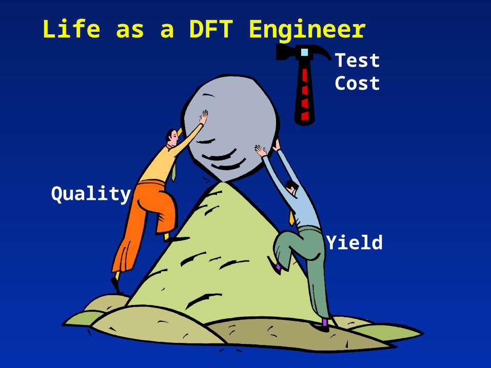
Life as a DFT Engineer
Yield
Quality
TestCost
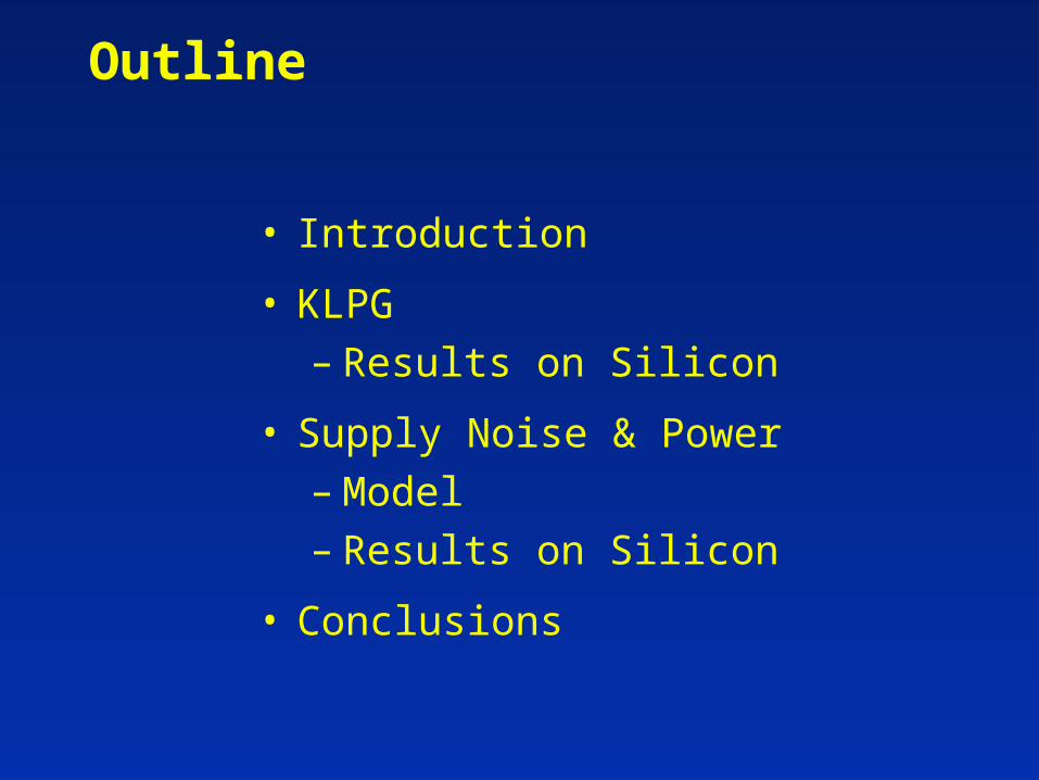
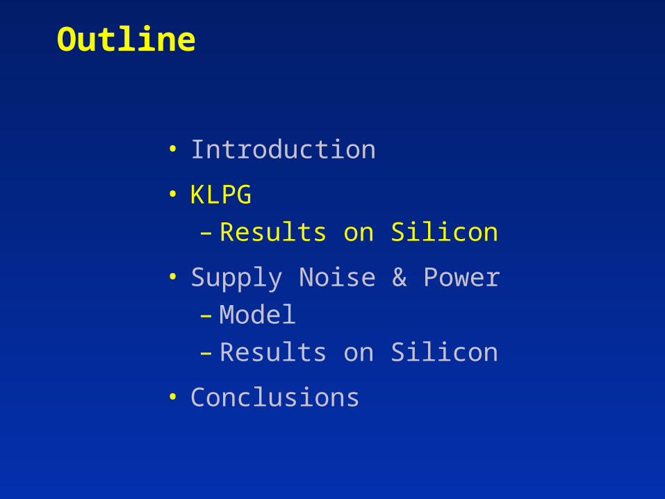
Outline
• Introduction
• KLPG– Results on Silicon
• Supply Noise & Power– Model– Results on Silicon
• Conclusions
0.1
1
10
100
2005 2010 2015 2020Year
Cost/Xistor
(μcents)
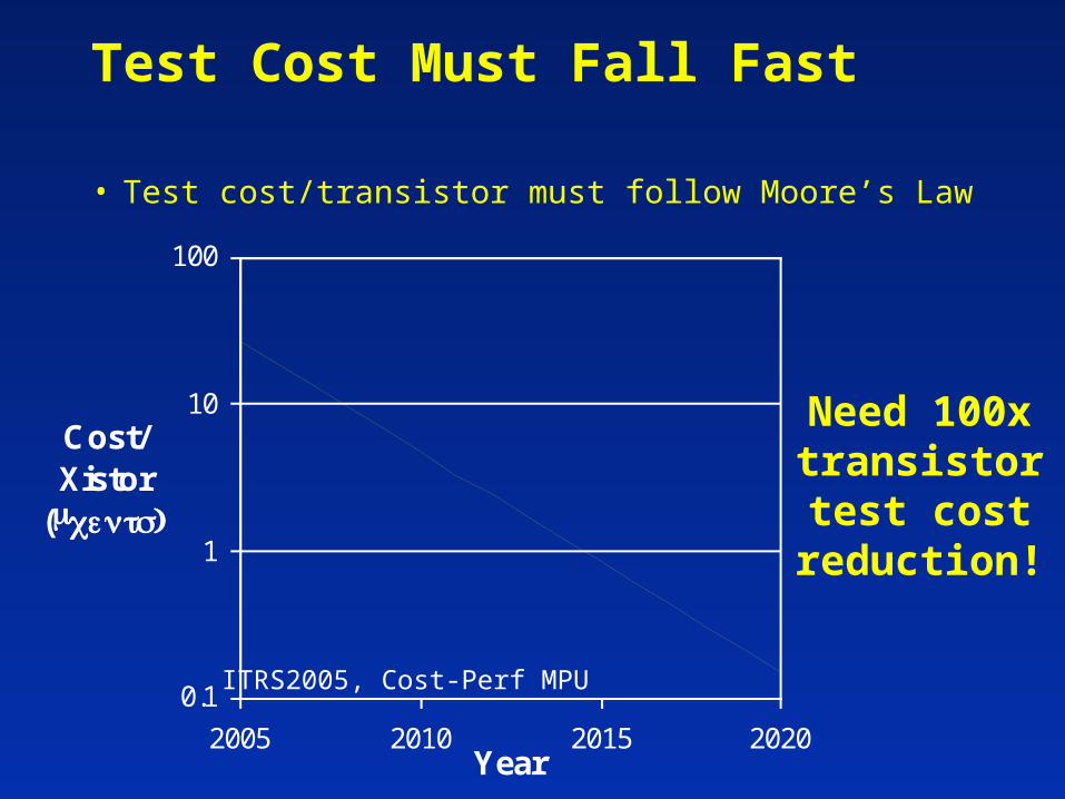
Test Cost Must Fall Fast
• Test cost/transistor must follow Moore’s Law
ITRS2005, Cost-Perf MPU
Need 100xtransistortest cost
reduction!
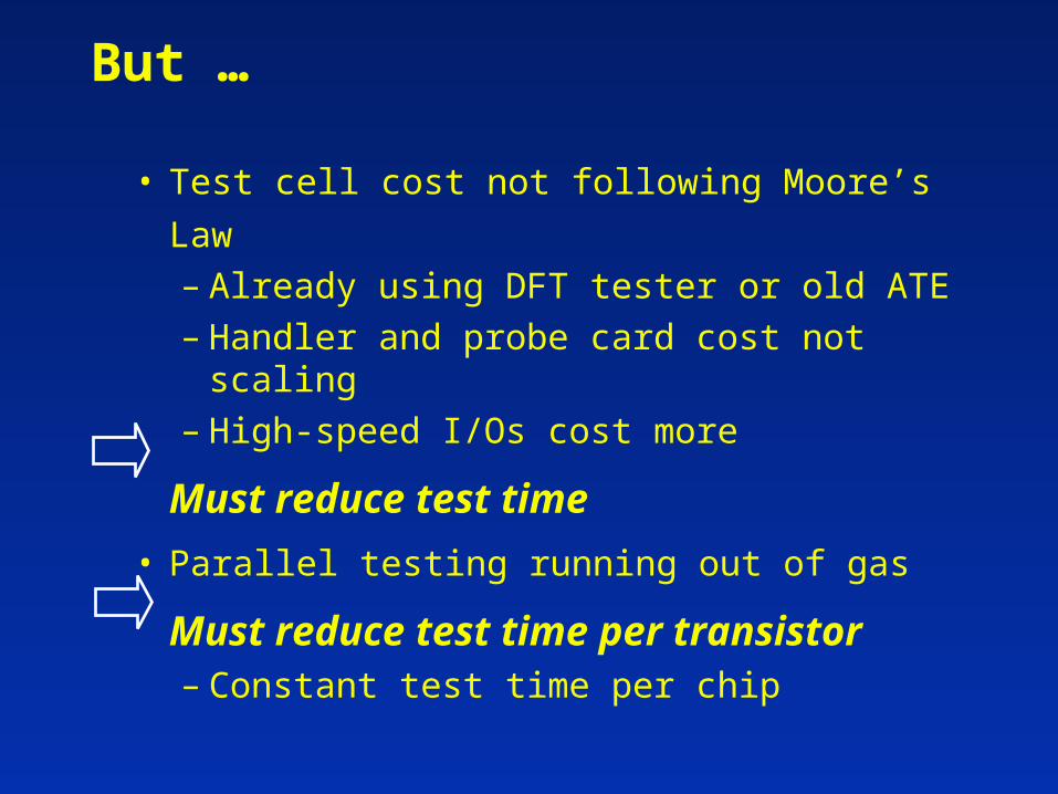
But …
• Test cell cost not following Moore’s Law– Already using DFT tester or old ATE– Handler and probe card cost not scaling– High-speed I/Os cost more
Must reduce test time
• Parallel testing running out of gas
Must reduce test time per transistor– Constant test time per chip
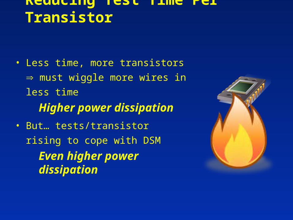
Reducing Test Time Per Transistor
• Less time, more transistors must
wiggle more wires in less time
Higher power dissipation
• But… tests/transistor rising to cope
with DSM
Even higher power dissipation
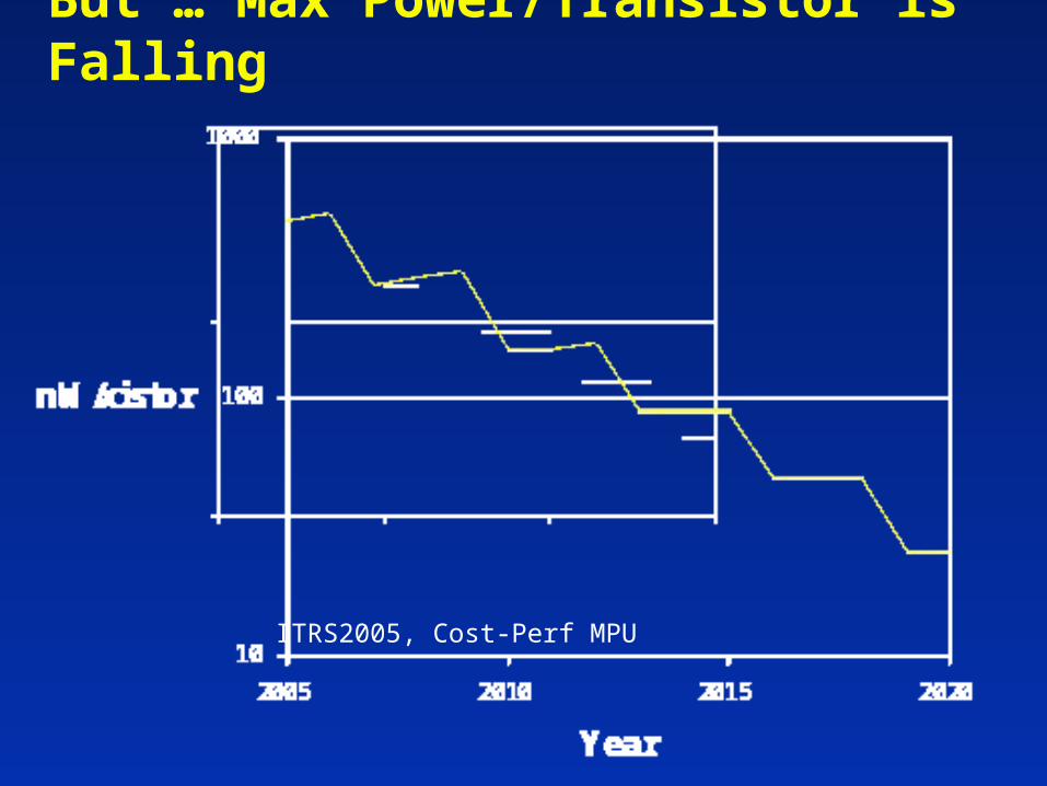
But … Max Power/Transistor is Falling
ITRS2005, Cost-Perf MPU
Future Digital Test All About Power?
• Fraction of chip that can be fired up at one
time is decreasing– Mission-mode power constraints– Test supply noise– Test thermal limits– Limits intra-die test parallelism
• How to screen most defects per Joule?
Eliminate Wasted Energy
• Useless transitions– Scan power– Unnecessary capture power– Much research/commercial activity
• Low-odds test patterns– Luck – tails of BIST, WRP– Shotgun blasts – N-detect, DOREME,
TARO, …
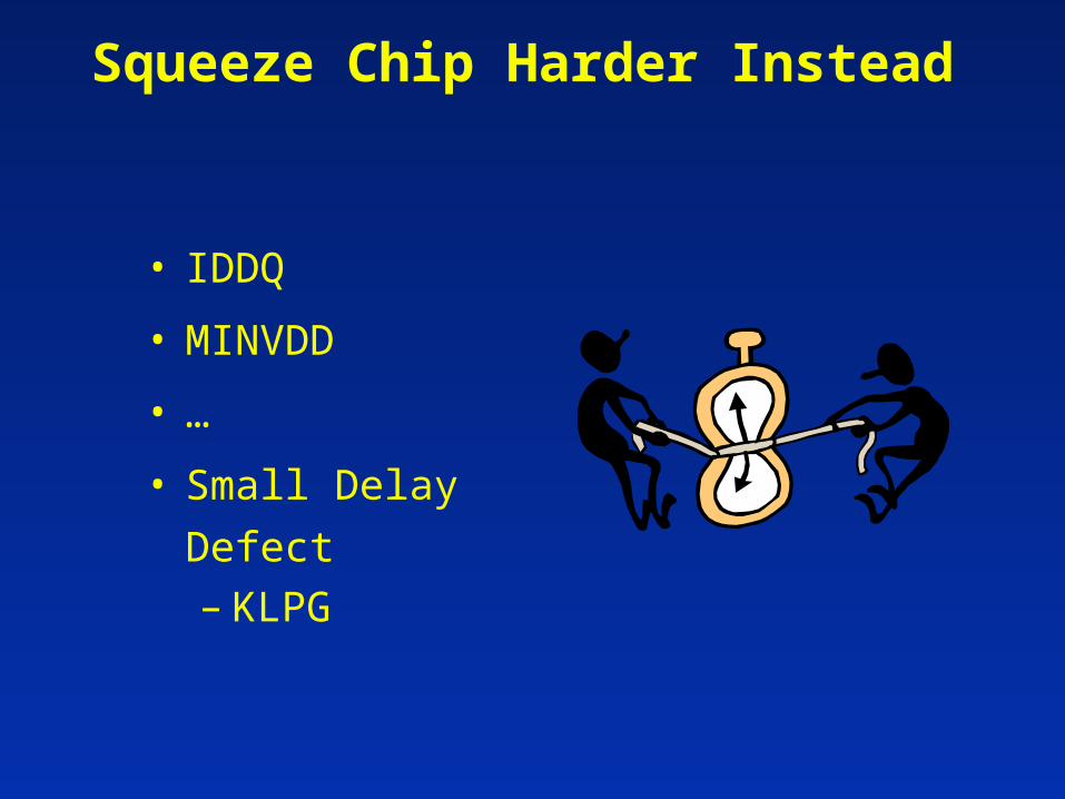
Squeeze Chip Harder Instead
• IDDQ
• MINVDD
• …
• Small Delay Defect– KLPG
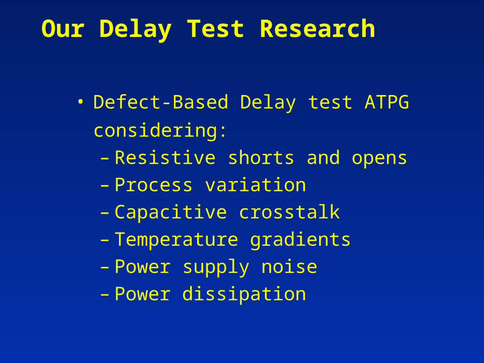
Our Delay Test Research
• Defect-Based Delay test ATPG considering:– Resistive shorts and opens– Process variation– Capacitive crosstalk– Temperature gradients– Power supply noise– Power dissipation
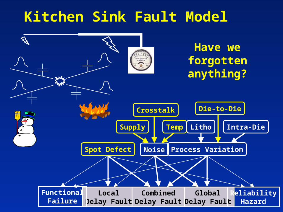
Kitchen Sink Fault Model
Spot Defect Process Variation
LocalDelay Fault
GlobalDelay Fault
CombinedDelay Fault
FunctionalFailure
ReliabilityHazard
Noise
Supply Temp
Crosstalk
Intra-Die
Die-to-Die
Litho
Have we forgotten anything?
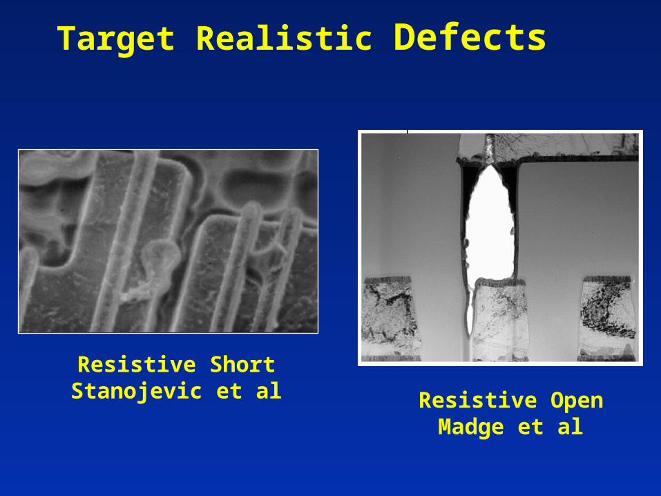
Target Realistic Defects
Resistive OpenMadge et al
Resistive ShortStanojevic et al
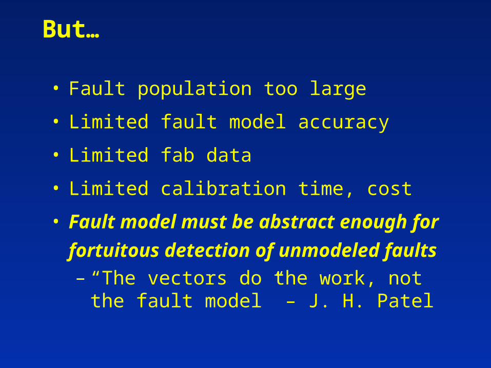
But…
• Fault population too large
• Limited fault model accuracy
• Limited fab data
• Limited calibration time, cost
• Fault model must be abstract enough for
fortuitous detection of unmodeled faults– “The vectors do the work, not the fault
model” – J. H. Patel
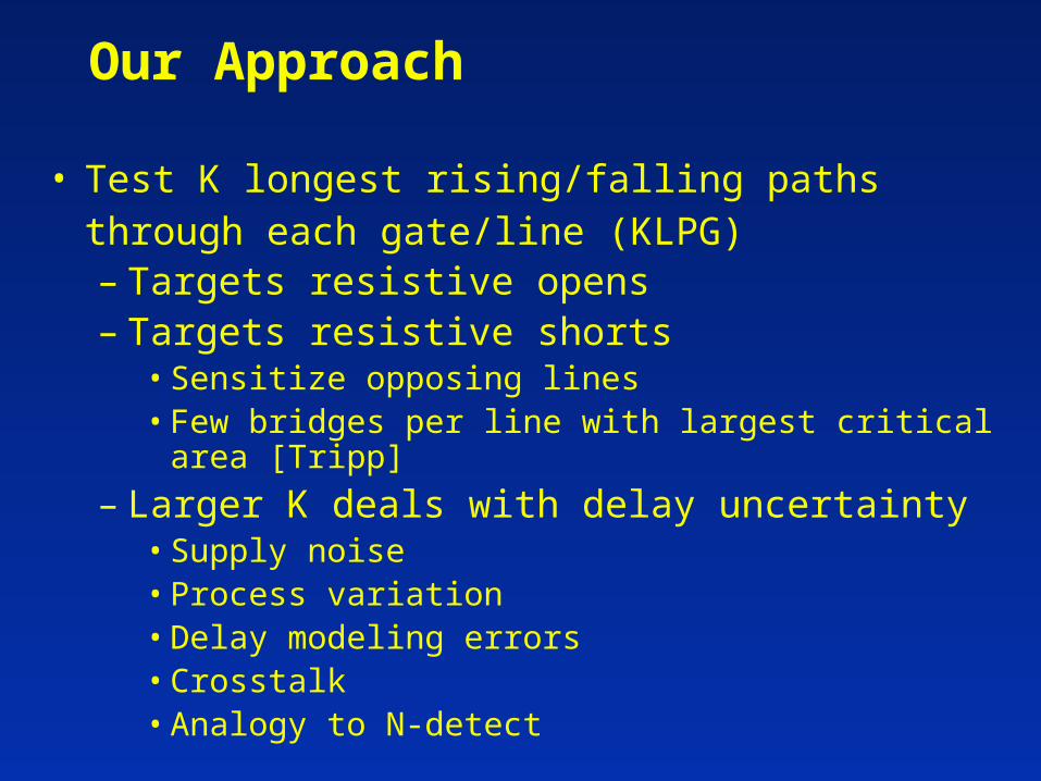
Our Approach
• Test K longest rising/falling paths through each gate/line (KLPG)– Targets resistive opens– Targets resistive shorts
• Sensitize opposing lines• Few bridges per line with largest critical area [Tripp]
– Larger K deals with delay uncertainty• Supply noise• Process variation• Delay modeling errors• Crosstalk• Analogy to N-detect
Outline
• Introduction
• KLPG– Results on Silicon
• Supply Noise & Power– Model– Results on Silicon
• Conclusions
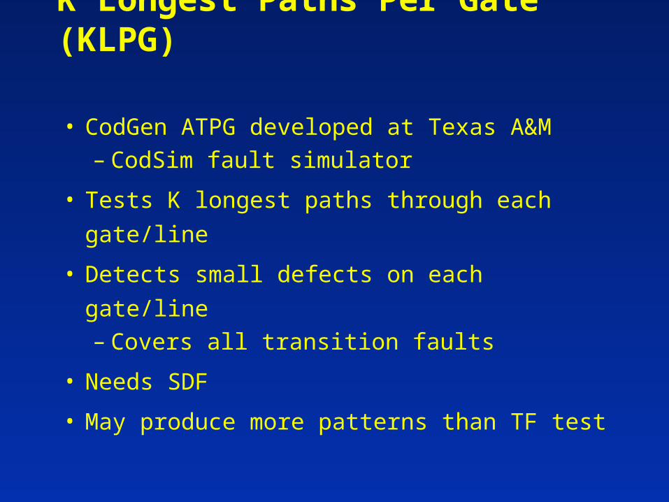
K Longest Paths Per Gate (KLPG)
• CodGen ATPG developed at Texas A&M– CodSim fault simulator
• Tests K longest paths through each gate/line
• Detects small defects on each gate/line– Covers all transition faults
• Needs SDF
• May produce more patterns than TF test
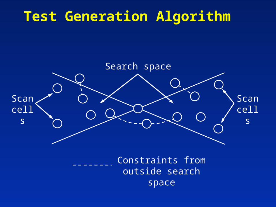
Test Generation Algorithm
Search space
Constraints from outside search space
Scan cells
Scan cells
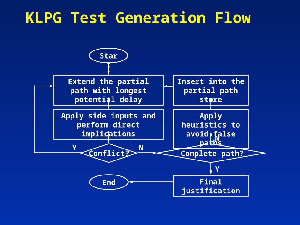
KLPG Test Generation Flow
Apply side inputs and perform direct implications
Conflict?
Start
Extend the partial path with longest potential delay
YComplete path?
N
Apply heuristics to avoid false paths
N
End Final justification
Y
Insert into the partial path store
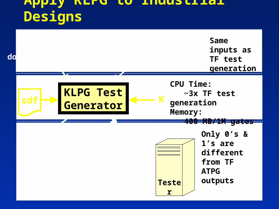
Apply KLPG to Industrial Designs
KLPG Test Generator
TetraMAX/FastScandofile/procfile/library
Hierarchical Verilog Design
K
Test Data
….010001100001....
Test Sequence……Load patternPulse clock......
Same inputs as TF test generation
Tester
sdf
CPU Time: ~3x TF test generationMemory: 400 MB/1M gates
Only 0’s & 1’s are different from TF ATPG outputs
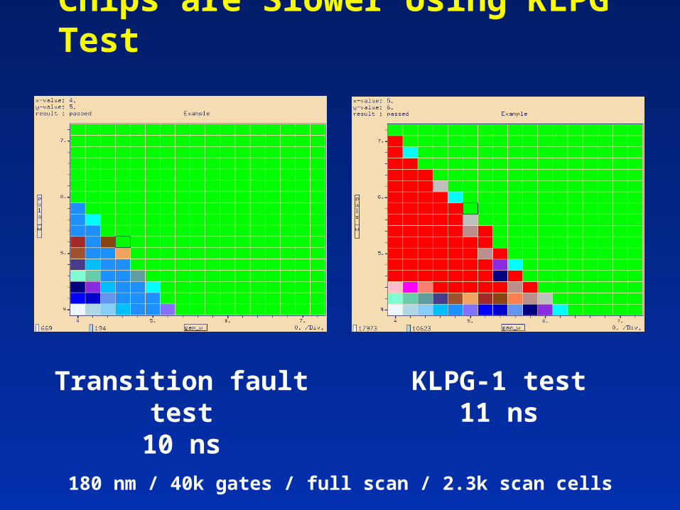
Transition fault test10 ns
KLPG-1 test11 ns
180 nm / 40k gates / full scan / 2.3k scan cells
Chips are Slower Using KLPG Test
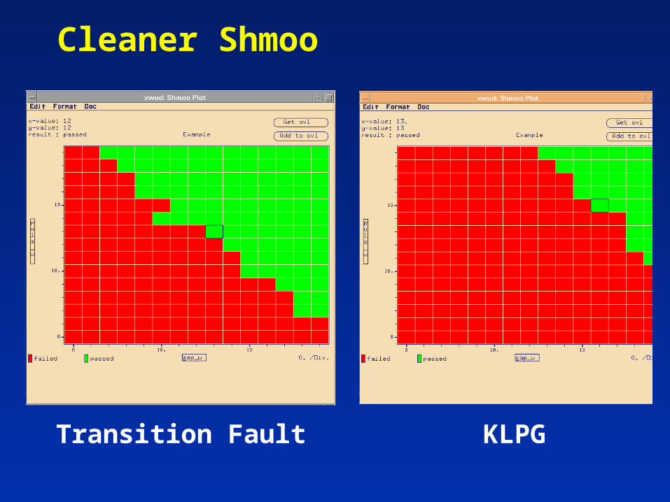
Cleaner Shmoo
Transition Fault KLPG
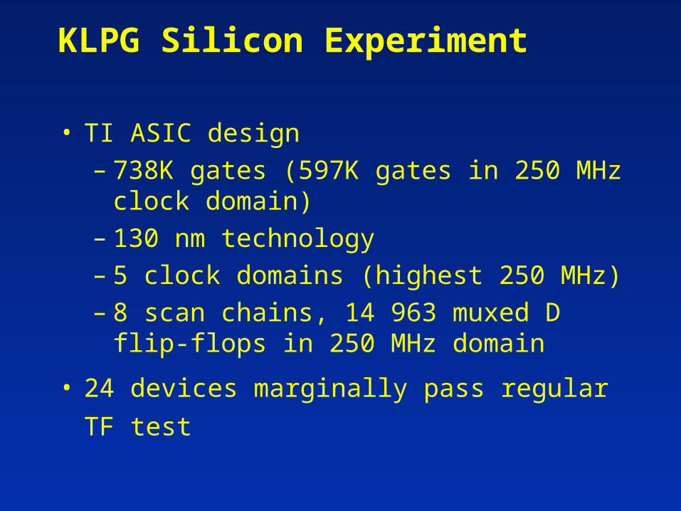
KLPG Silicon Experiment
• TI ASIC design– 738K gates (597K gates in 250 MHz clock
domain)– 130 nm technology– 5 clock domains (highest 250 MHz)– 8 scan chains, 14 963 muxed D flip-flops in
250 MHz domain
• 24 devices marginally pass regular TF test
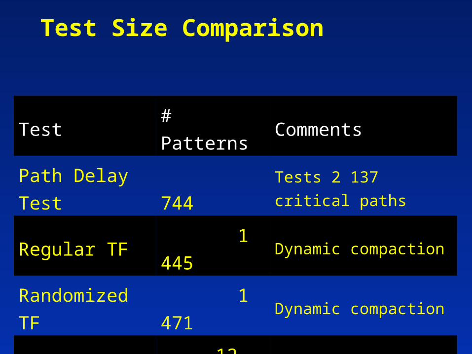
Test Size Comparison
Test # Patterns Comments
Path Delay Test 744 Tests 2 137 critical paths
Regular TF 1 445 Dynamic compaction
Randomized TF 1 471 Dynamic compaction
KLPG-1 12 579 Static compaction
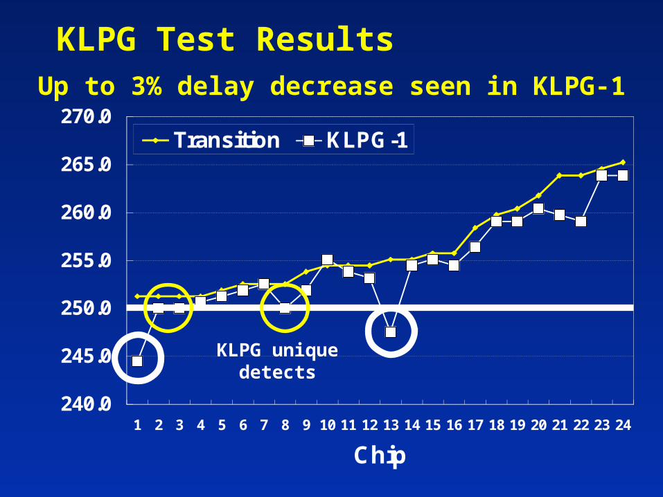
240.0
245.0
250.0
255.0
260.0
265.0
270.0
1 2 3 4 5 6 7 8 9 10 11 12 13 14 15 16 17 18 19 20 21 22 23 24
Chip
Fmax (MHz)
Transition KLPG-1
KLPG Test Results
KLPG unique detects
Up to 3% delay decrease seen in KLPG-1
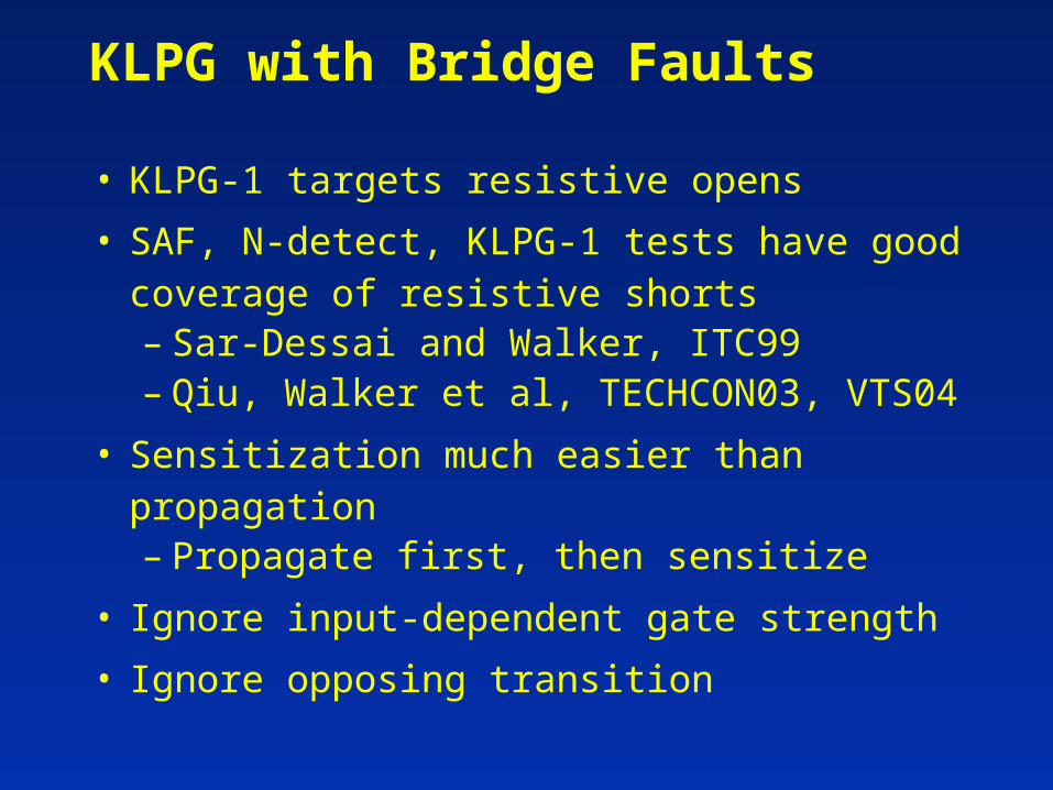
KLPG with Bridge Faults
• KLPG-1 targets resistive opens
• SAF, N-detect, KLPG-1 tests have good coverage of resistive shorts– Sar-Dessai and Walker, ITC99– Qiu, Walker et al, TECHCON03, VTS04
• Sensitization much easier than propagation– Propagate first, then sensitize
• Ignore input-dependent gate strength
• Ignore opposing transition
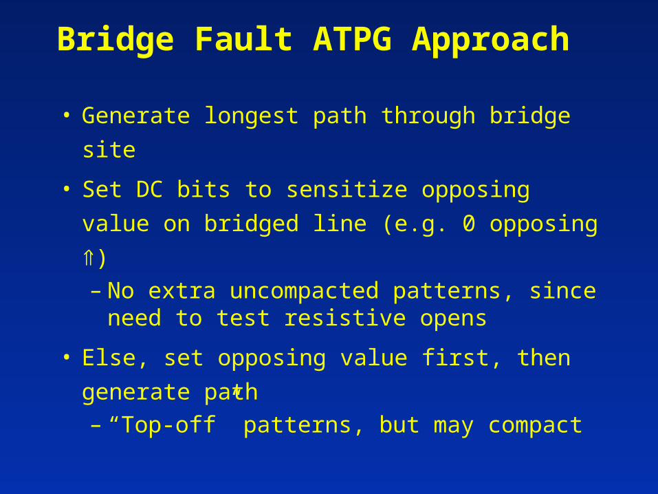
Bridge Fault ATPG Approach
• Generate longest path through bridge site
• Set DC bits to sensitize opposing value on
bridged line (e.g. 0 opposing )– No extra uncompacted patterns, since
need to test resistive opens
• Else, set opposing value first, then generate
path– “Top-off” patterns, but may compact
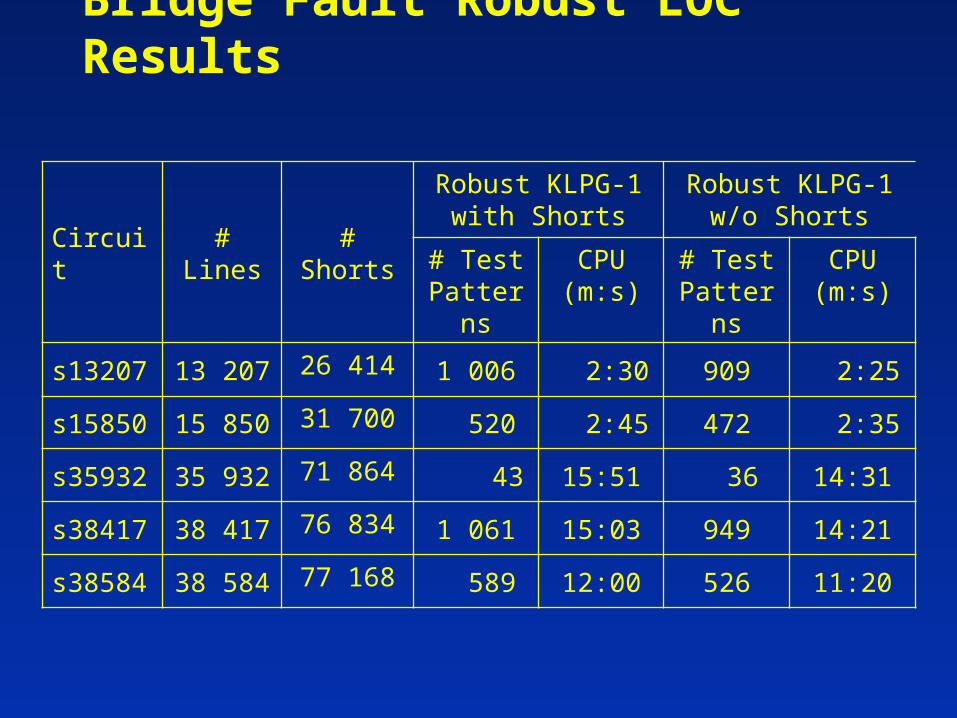
Bridge Fault Robust LOC Results
Circuit # Lines # Shorts
Robust KLPG-1 with Shorts
Robust KLPG-1 w/o Shorts
# Test Patterns
CPU (m:s)
# Test Patterns
CPU (m:s)
s13207 13 207 26 414 1 006 2:30 909 2:25
s15850 15 850 31 700 520 2:45 472 2:35
s35932 35 932 71 864 43 15:51 36 14:31
s38417 38 417 76 834 1 061 15:03 949 14:21
s38584 38 584 77 168 589 12:00 526 11:20
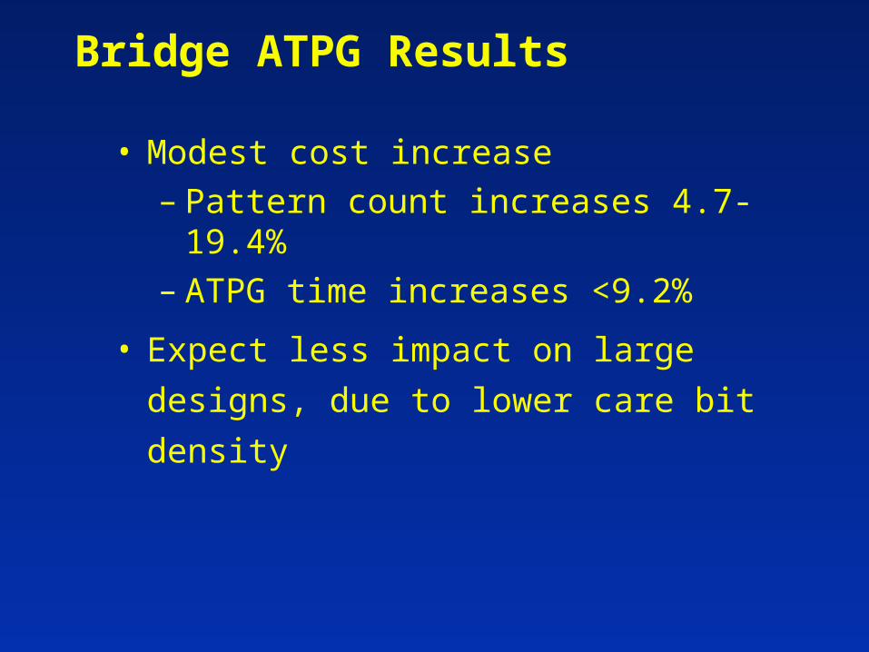
Bridge ATPG Results
• Modest cost increase– Pattern count increases 4.7-19.4%– ATPG time increases <9.2%
• Expect less impact on large designs, due to
lower care bit density
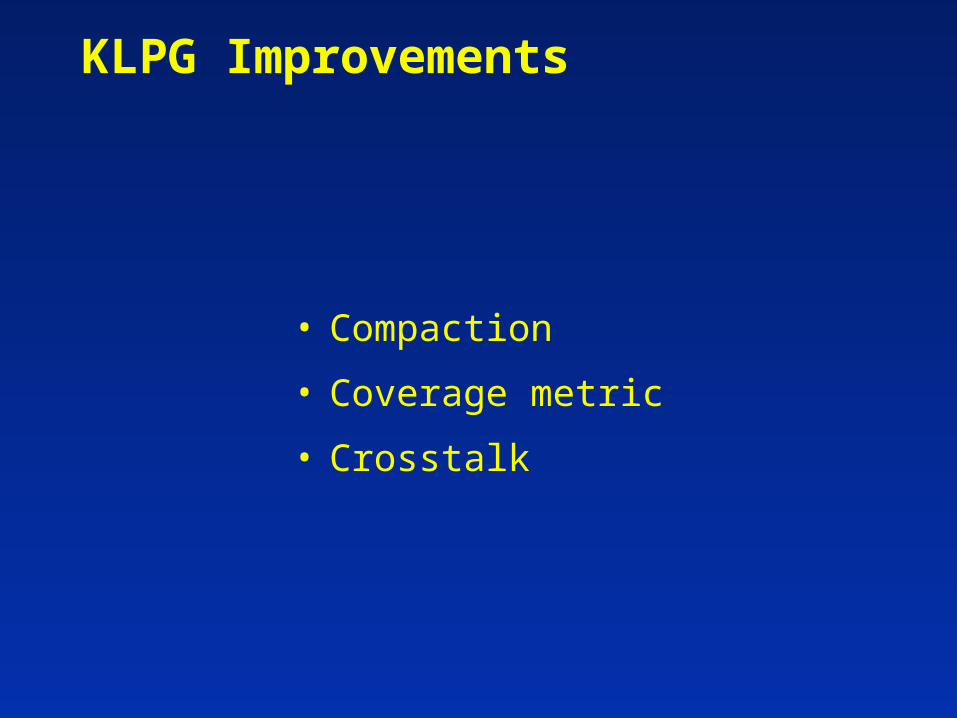
KLPG Improvements
• Compaction
• Coverage metric
• Crosstalk
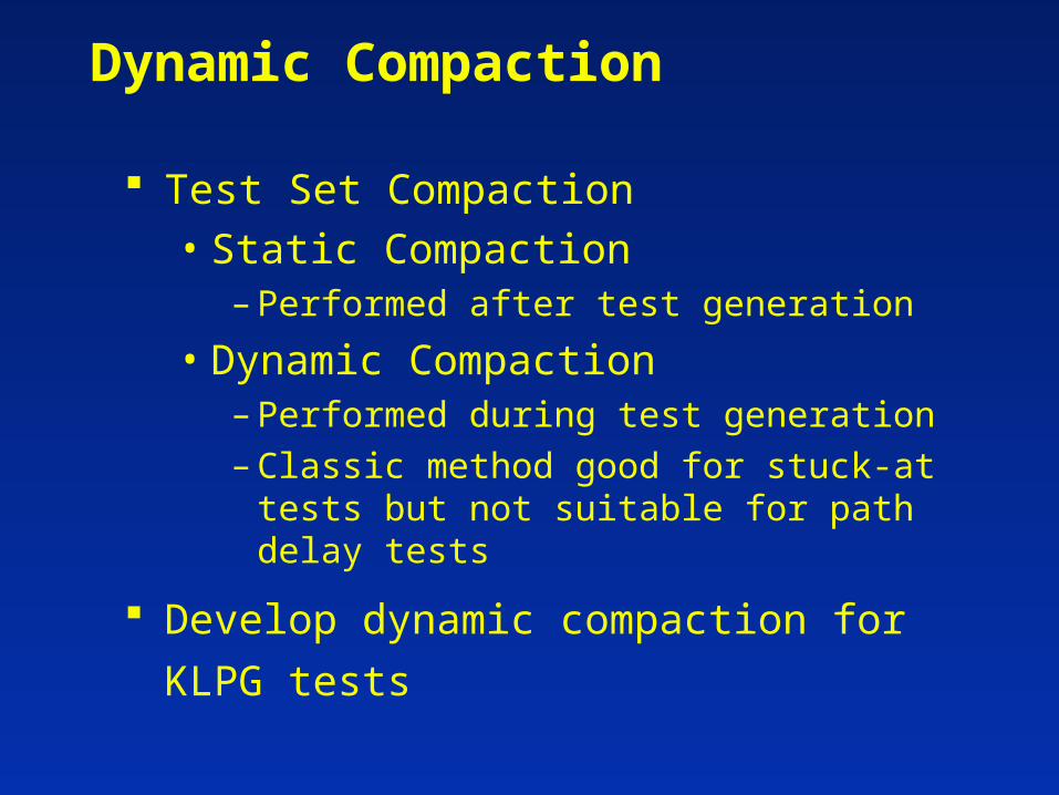
Dynamic Compaction
Test Set Compaction• Static Compaction
– Performed after test generation
• Dynamic Compaction– Performed during test generation– Classic method good for stuck-at tests but not
suitable for path delay tests
Develop dynamic compaction for KLPG tests
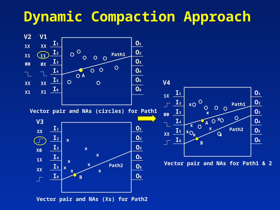
Dynamic Compaction Approach
Vector pair and NAs (Xs) for Path2
V3
XX
1X
X0
XX
I1
I2
I3
I4
I5
I6
O1
O2
O3
O4
O5
O6
xx
x xx Path2
x
B
x
x
O2
O3
O6
O5
Vector pair and NAs for Path1 & 2
V4
I1
I2
I3
I4
I5
I6
O1
O4
Path1
1X
00
XX
Ax
x
x xx Path2
x
B
x
x
Vector pair and NAs (circles) for Path1
V2 V1I1
I2
I3
I4
I5
I6
O1
O2
O3
O4
O5
O6
Path1
XX
11
0X
X1
XX
1X
X1
00
X1
XX
A

Dynamic Compaction Algorithm
• Definitions:
– vector : output for ATE
– pattern : a set of necessary assignments associated with one or more paths
– POOL : a data structure to save patterns
• Check the compatibility between necessary assignments of new path against a pattern in the POOL
• Generation of final test vector is postponed until test generation is finished
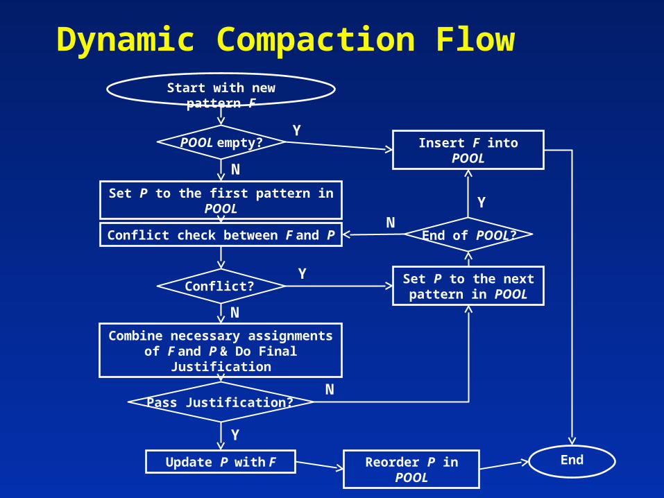
Dynamic Compaction FlowStart with new pattern F
POOL empty?
Conflict check between F and P
Conflict?
Pass Justification?
End of POOL?
Set P to the next pattern in POOL
Y
YSet P to the first pattern in POOL
N
Combine necessary assignments of F and P & Do Final Justification
N
N
N
Y
End
Insert F into POOL
Update P with F
Y
Reorder P in POOL
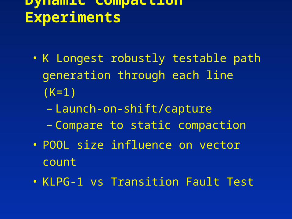
Dynamic Compaction Experiments
• K Longest robustly testable path generation
through each line (K=1)– Launch-on-shift/capture– Compare to static compaction
• POOL size influence on vector count
• KLPG-1 vs Transition Fault Test
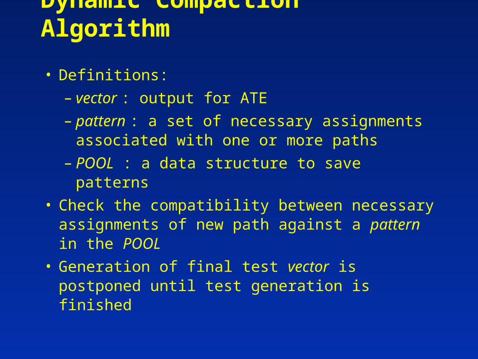
Dynamic Compaction Algorithm
• Definitions:
– vector : output for ATE
– pattern : a set of necessary assignments associated with one or more paths
– POOL : a data structure to save patterns
• Check the compatibility between necessary assignments of new path against a pattern in the POOL
• Generation of final test vector is postponed until test generation is finished
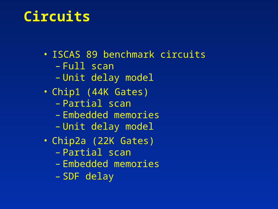
Circuits
• ISCAS 89 benchmark circuits– Full scan– Unit delay model
• Chip1 (44K Gates)– Partial scan– Embedded memories– Unit delay model
• Chip2a (22K Gates)– Partial scan– Embedded memories– SDF delay
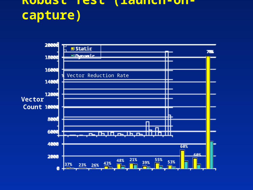
Robust Test (launch-on-capture)
37% 23% 26% 43%48% 21%
39%55%
53%
60%
60%
% Vector Reduction Rate
VectorCount
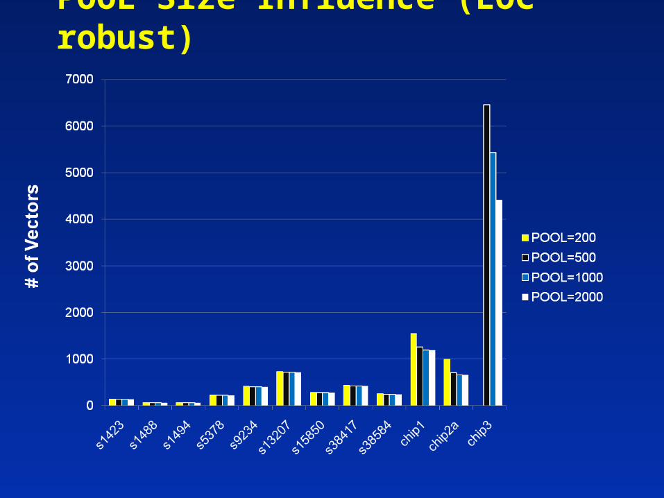
POOL Size Influence (LOC robust)
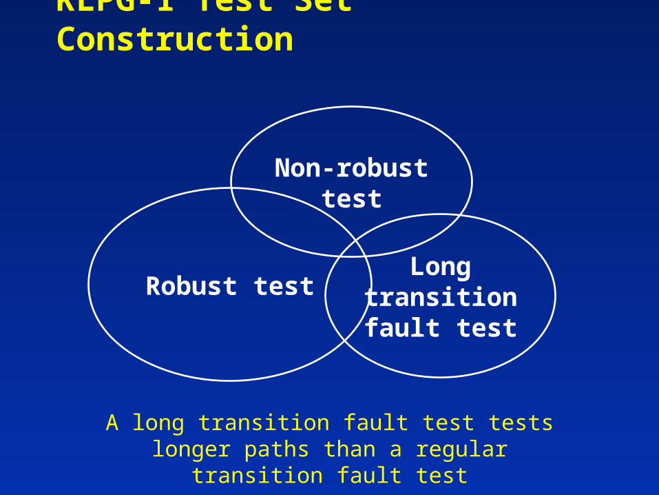
KLPG-1 Test Set Construction
Robust test
Non-robusttest
Longtransitionfault test
A long transition fault test tests longer paths than a regular transition fault test
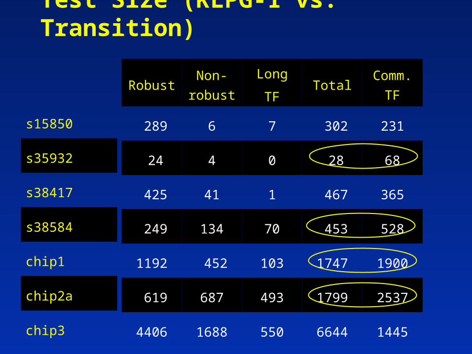
Test Size (KLPG-1 vs. Transition)
RobustNon-
robust
Long
TFTotal
Comm.
TF
289 6 7 302 231
24 4 0 28 68
425 41 1 467 365
249 134 70 453 528
1192 452 103 1747 1900
619 687 493 1799 2537
4406 1688 550 6644 1445
s15850
s35932
s38417
s38584
chip1
chip2a
chip3
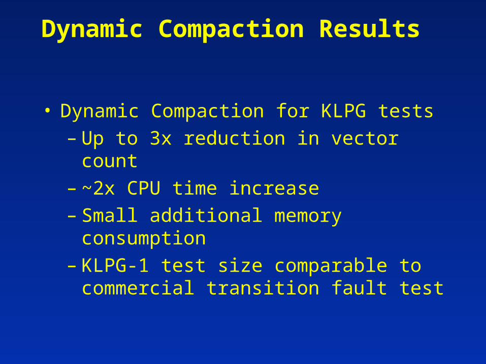
Dynamic Compaction Results
• Dynamic Compaction for KLPG tests– Up to 3x reduction in vector count– ~2x CPU time increase– Small additional memory consumption– KLPG-1 test size comparable to
commercial transition fault test
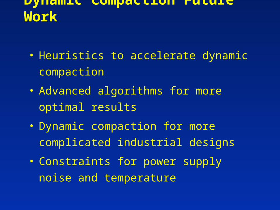
Dynamic Compaction Future Work
• Heuristics to accelerate dynamic compaction
• Advanced algorithms for more optimal results
• Dynamic compaction for more complicated
industrial designs
• Constraints for power supply noise and
temperature
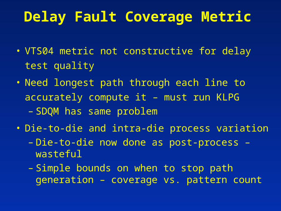
Delay Fault Coverage Metric
• VTS04 metric not constructive for delay test
quality
• Need longest path through each line to accurately
compute it – must run KLPG– SDQM has same problem
• Die-to-die and intra-die process variation– Die-to-die now done as post-process – wasteful– Simple bounds on when to stop path generation
– coverage vs. pattern count
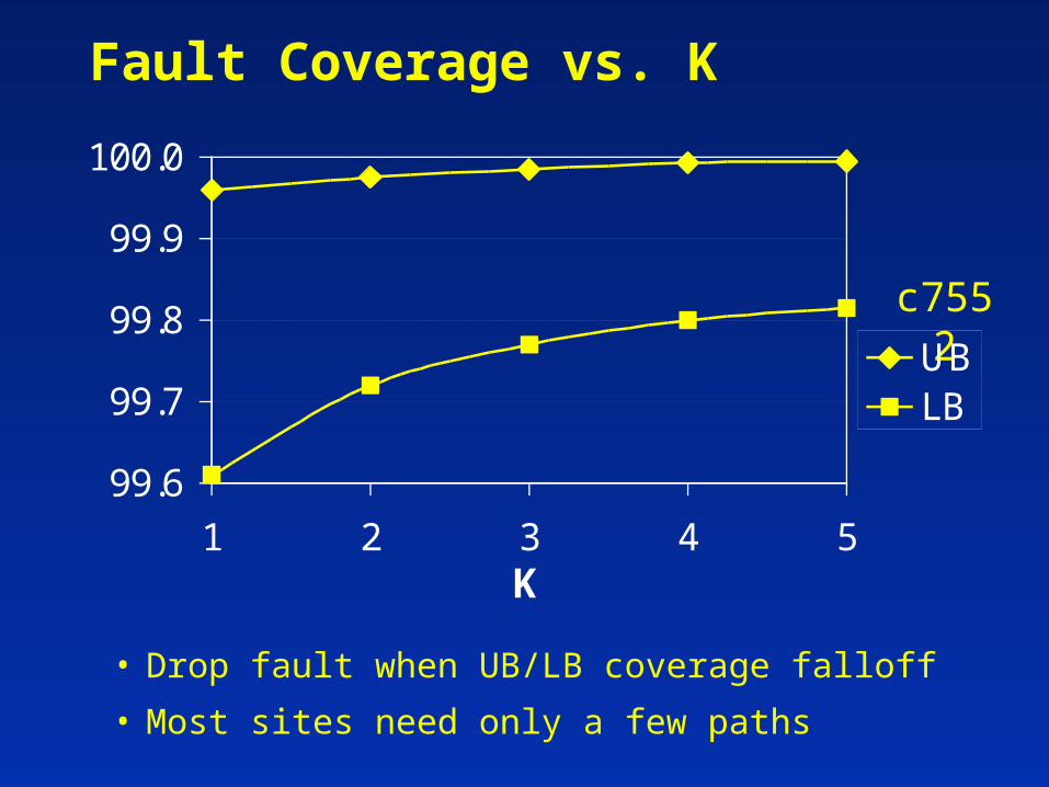
Fault Coverage vs. K
• Drop fault when UB/LB coverage falloff
• Most sites need only a few paths
c7552
99.6
99.7
99.8
99.9
100.0
1 2 3 4 5K
UBLB
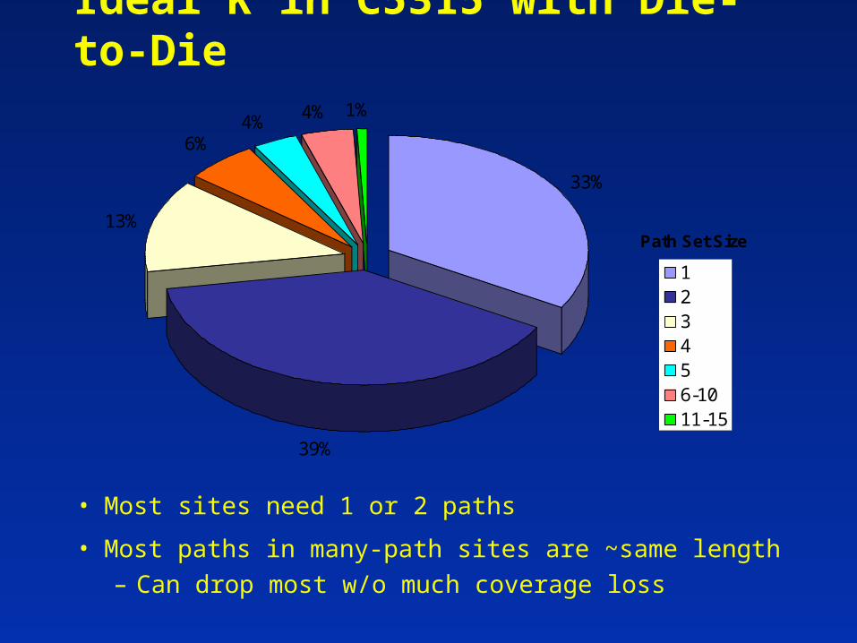
Ideal K in C5315 with Die-to-Die
• Most sites need 1 or 2 paths
• Most paths in many-path sites are ~same length– Can drop most w/o much coverage loss
33%
39%
13%
6%4% 4% 1%
123456-1011-15
Path Set Size
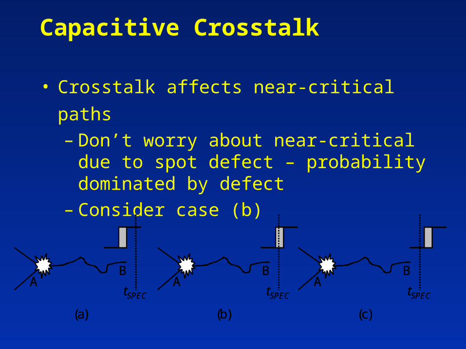
Capacitive Crosstalk
• Crosstalk affects near-critical paths– Don’t worry about near-critical due to spot
defect – probability dominated by defect– Consider case (b)
A given vector pair is applied
AB
tSPECA
BA
B
(a)
tSPEC
(b)
tSPEC
(c)
A given vector pair is applied
AB
tSPECA
BA
B
(a)
tSPEC
(b)
tSPEC
(c)
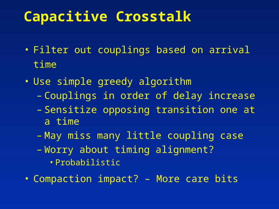
Capacitive Crosstalk
• Filter out couplings based on arrival time
• Use simple greedy algorithm– Couplings in order of delay increase– Sensitize opposing transition one at a time– May miss many little coupling case– Worry about timing alignment?
• Probabilistic
• Compaction impact? – More care bits
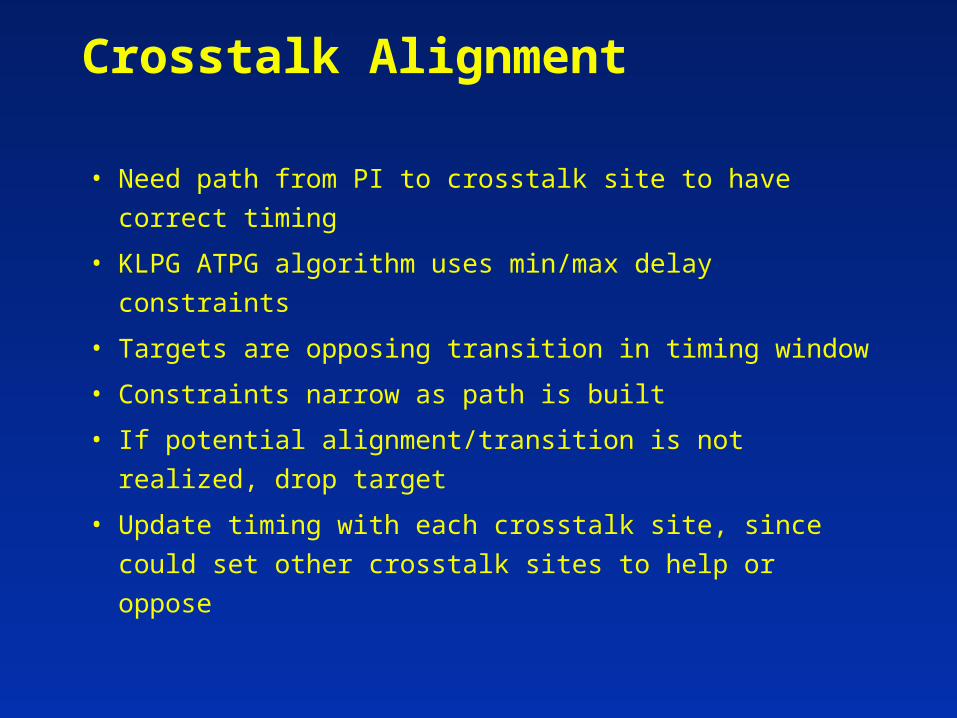
Crosstalk Alignment
• Need path from PI to crosstalk site to have correct
timing
• KLPG ATPG algorithm uses min/max delay
constraints
• Targets are opposing transition in timing window
• Constraints narrow as path is built
• If potential alignment/transition is not realized, drop
target
• Update timing with each crosstalk site, since could
set other crosstalk sites to help or oppose
Outline
• Introduction
• KLPG– Results on Silicon
• Supply Noise & Power– Model– Results on Silicon
• Conclusions
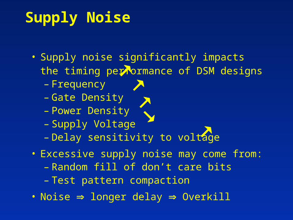
Supply Noise
• Supply noise significantly impacts the timing performance of DSM designs– Frequency– Gate Density– Power Density– Supply Voltage– Delay sensitivity to voltage
• Excessive supply noise may come from:– Random fill of don’t care bits – Test pattern compaction
• Noise longer delay Overkill
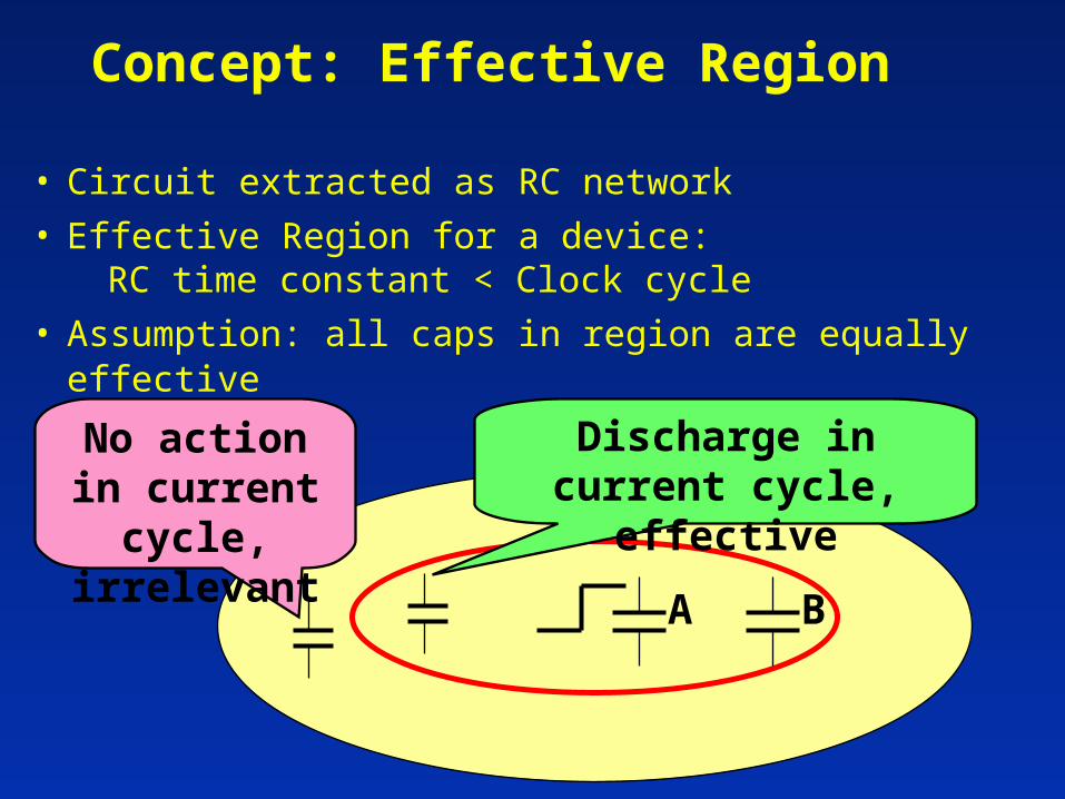
Concept: Effective Region
• Circuit extracted as RC network
• Effective Region for a device: RC time constant < Clock cycle
• Assumption: all caps in region are equally effective
Discharge in current cycle, effective
No action in current cycle,
irrelevant
A B
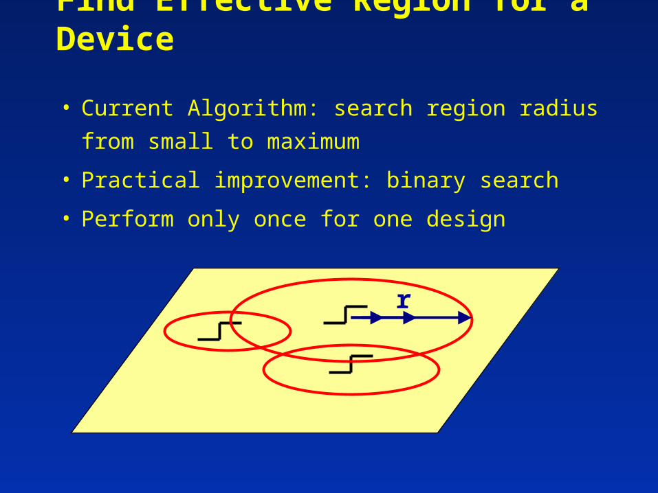
Find Effective Region for a Device
• Current Algorithm: search region radius from small
to maximum
• Practical improvement: binary search
• Perform only once for one design
r
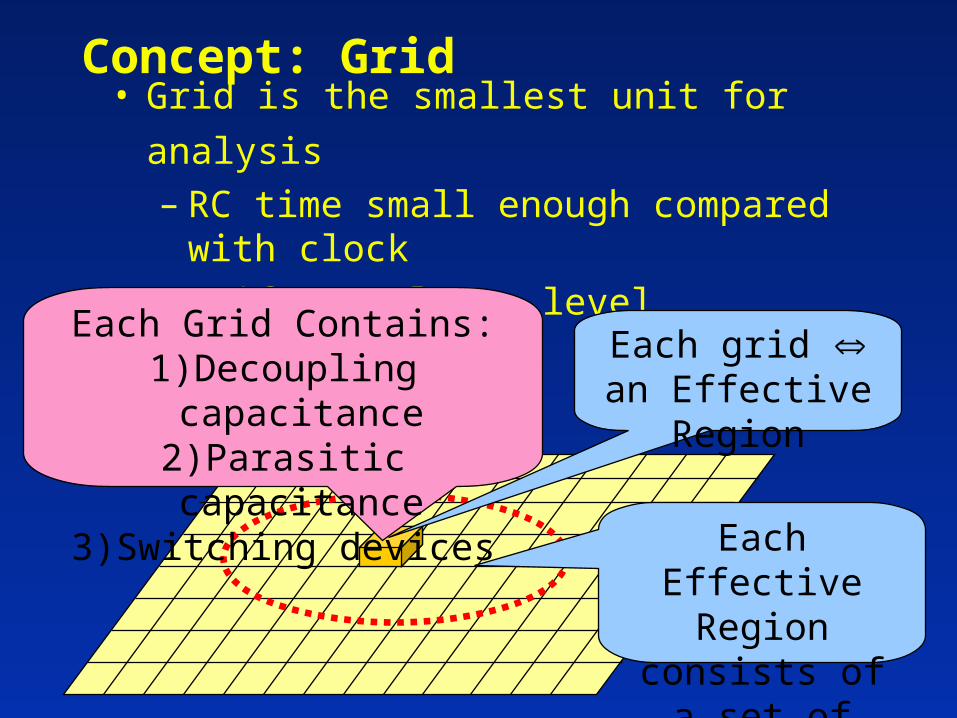
Concept: Grid
• Grid is the smallest unit for analysis– RC time small enough compared with clock – Uniform voltage level
Each Grid Contains:1)Decoupling capacitance
2)Parasitic capacitance3)Switching devices
Each grid an Effective Region
Each Effective Region consists of a set of grids
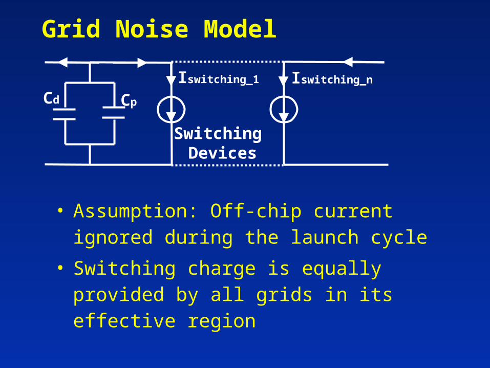
Grid Noise Model
• Assumption: Off-chip current ignored during the launch cycle
• Switching charge is equally provided by all grids in its effective region
Cd Cp
Iswitching_1 Iswitching_n
Switching Devices
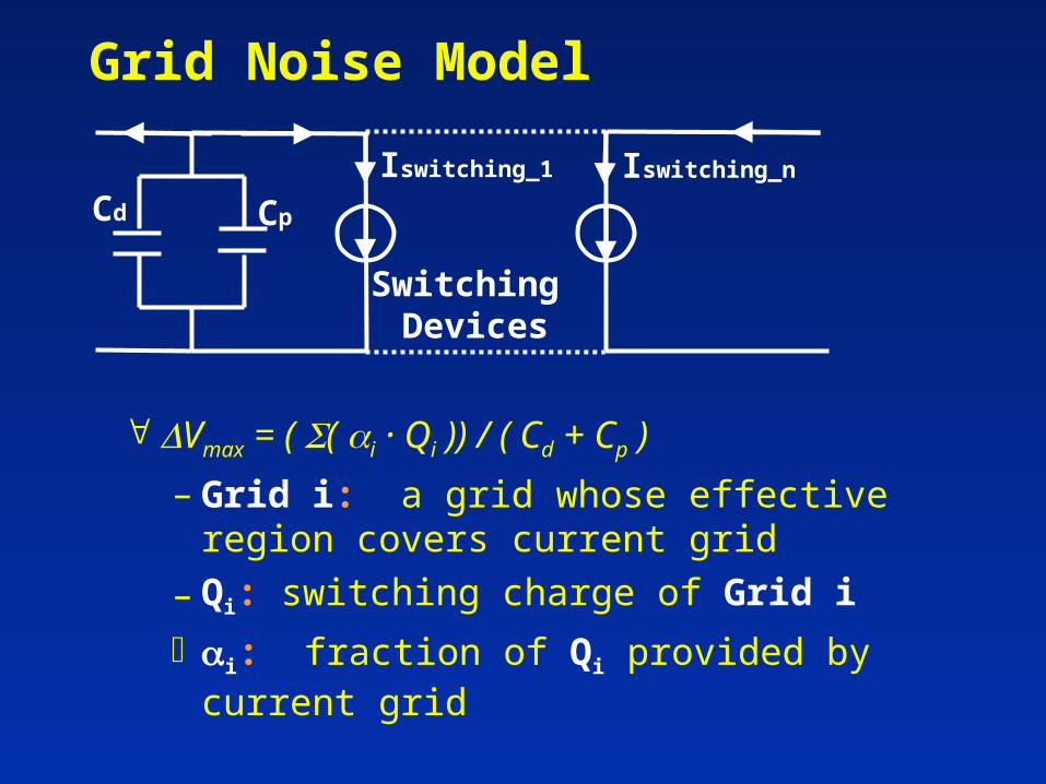
Grid Noise Model
Vmax = ( ( i · Qi )) / ( Cd + Cp )
– Grid i: a grid whose effective region covers current grid
– Qi: switching charge of Grid i
i: fraction of Qi provided by current grid
Cd Cp
Iswitching_1 Iswitching_n
Switching Devices
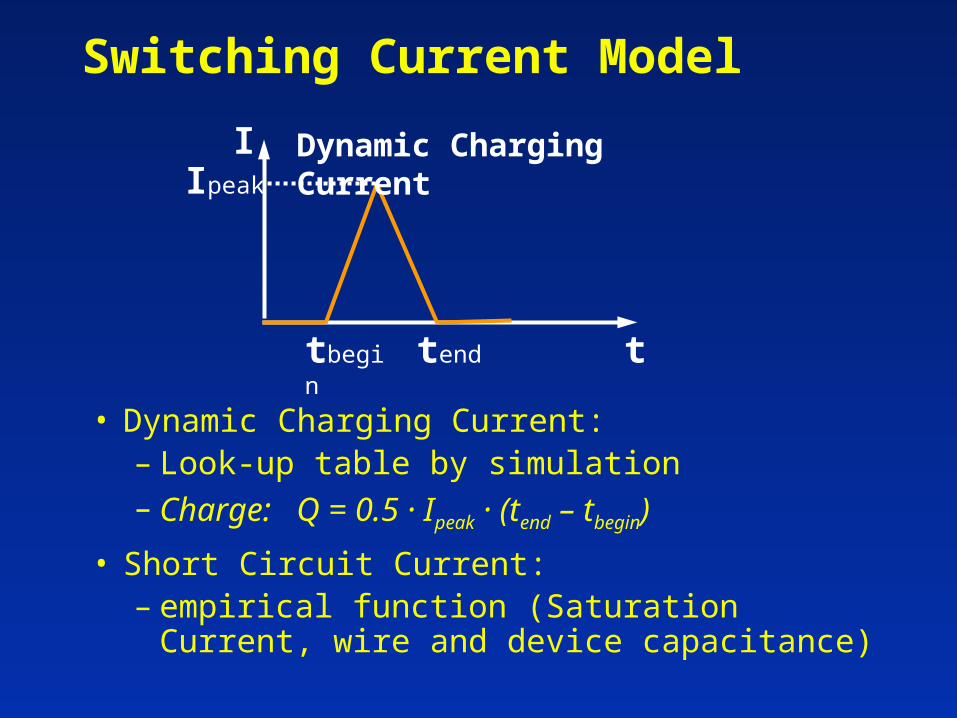
Switching Current Model
• Dynamic Charging Current: – Look-up table by simulation – Charge: Q = 0.5 · Ipeak · (tend – tbegin)
• Short Circuit Current: – empirical function (Saturation Current, wire
and device capacitance)
I
ttbegin tend
Ipeak
Dynamic Charging Current
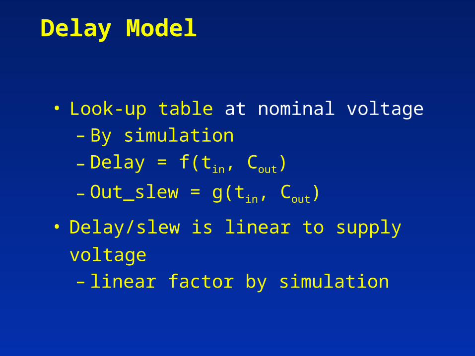
Delay Model
• Look-up table at nominal voltage– By simulation
– Delay = f(tin, Cout)
– Out_slew = g(tin, Cout)
• Delay/slew is linear to supply voltage– linear factor by simulation
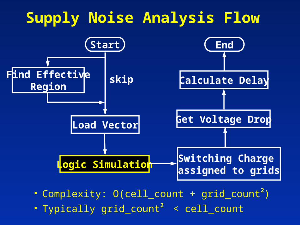
Supply Noise Analysis Flow
Start End
Load Vector
Logic Simulation
Get Voltage Drop
Calculate DelayFind Effective
Regionskip
Switching Charge assigned to grids
• Complexity: O(cell_count + grid_count2)
• Typically grid_count2 < cell_count
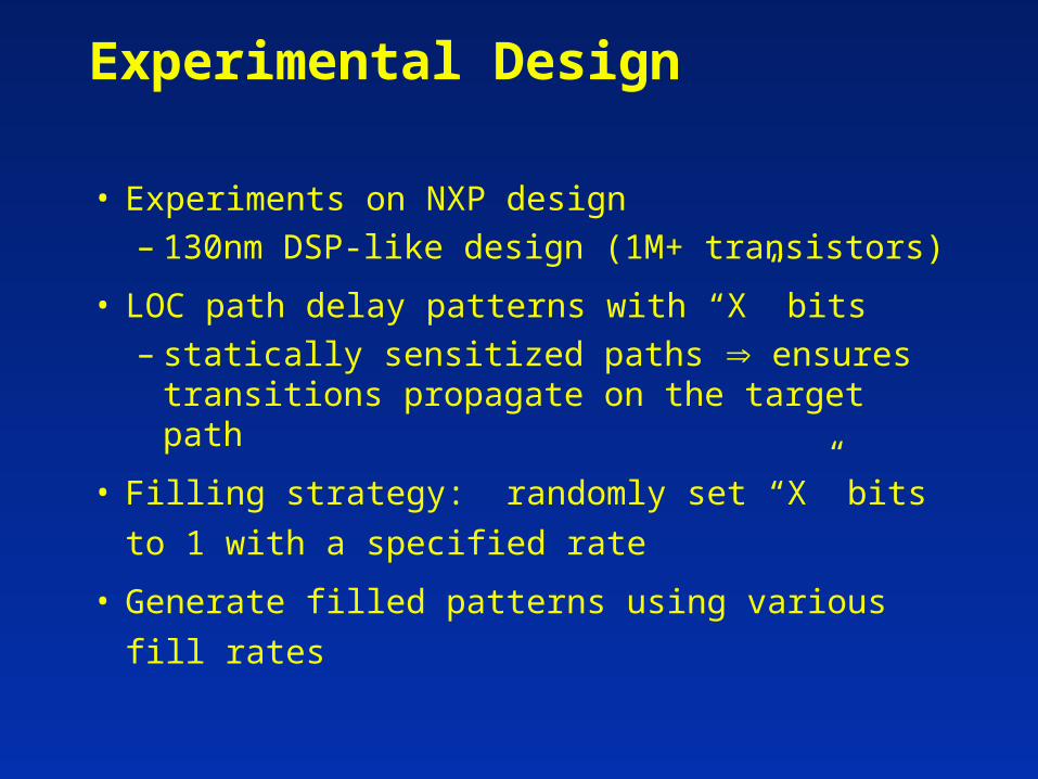
Experimental Design
• Experiments on NXP design– 130nm DSP-like design (1M+ transistors)
• LOC path delay patterns with “X” bits– statically sensitized paths ensures
transitions propagate on the target path
• Filling strategy: randomly set “X” bits to 1
with a specified rate
• Generate filled patterns using various fill rates
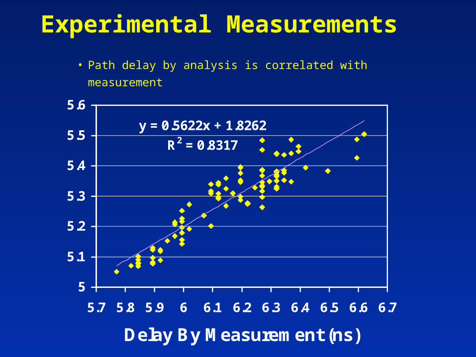
Experimental Measurements
• Path delay by analysis is correlated with measurement
y = 0.5622x + 1.8262
R2 = 0.8317
5
5.1
5.2
5.3
5.4
5.5
5.6
5.7 5.8 5.9 6 6.1 6.2 6.3 6.4 6.5 6.6 6.7
Delay By Measurement (ns)
By Analysis (ns)
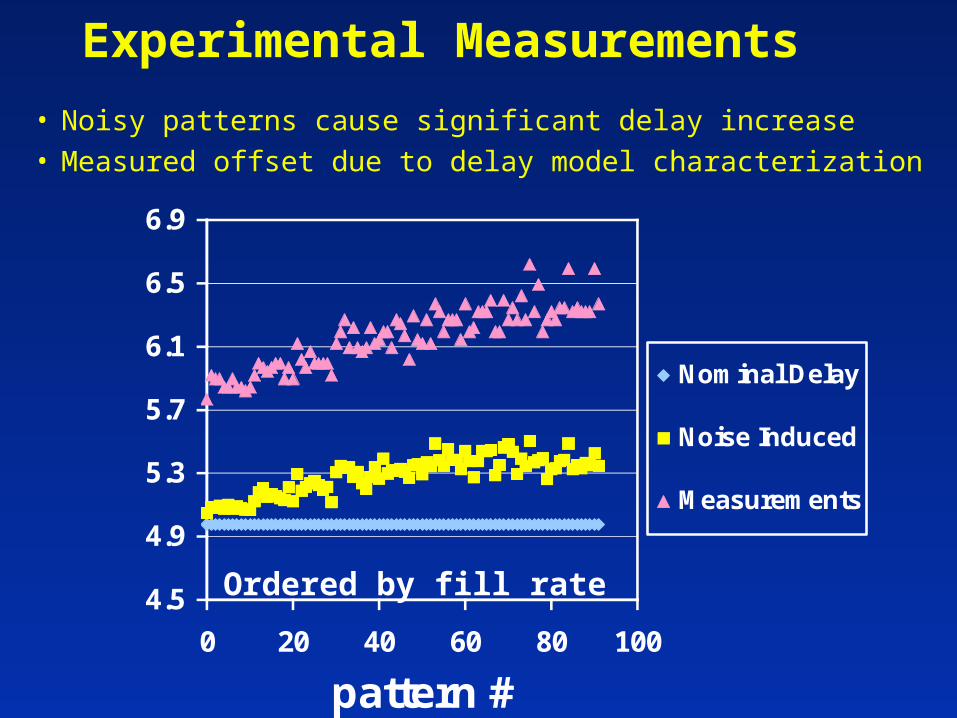
Experimental Measurements
• Noisy patterns cause significant delay increase• Measured offset due to delay model characterization
Ordered by fill rate4.5
4.9
5.3
5.7
6.1
6.5
6.9
0 20 40 60 80 100
pattern #
Delay (ns)
Nominal Delay
Noise Induced
Measurements
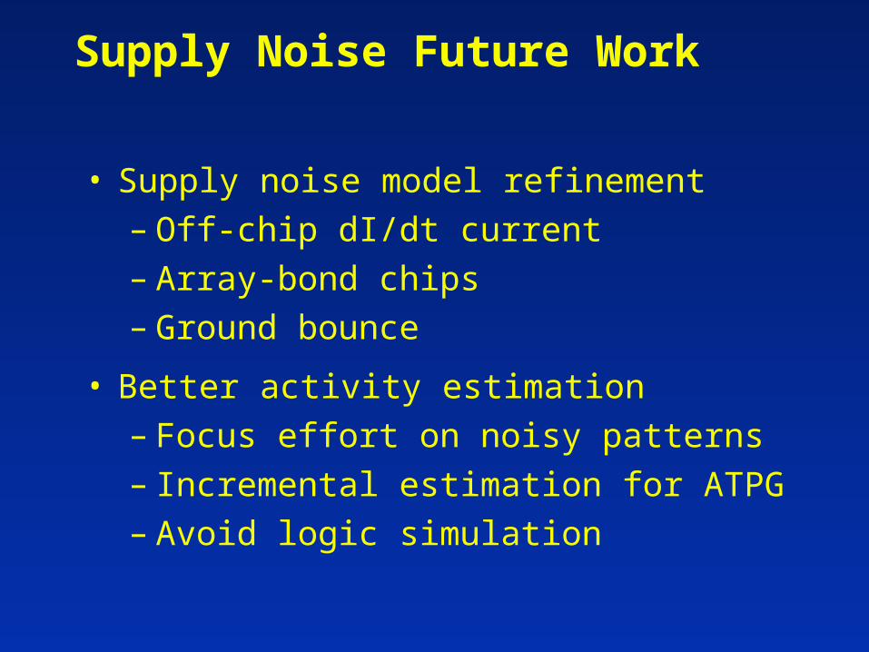
Supply Noise Future Work
• Supply noise model refinement– Off-chip dI/dt current– Array-bond chips– Ground bounce
• Better activity estimation– Focus effort on noisy patterns– Incremental estimation for ATPG– Avoid logic simulation
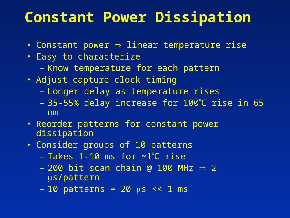
Constant Power Dissipation
• Constant power linear temperature rise• Easy to characterize
– Know temperature for each pattern• Adjust capture clock timing
– Longer delay as temperature rises– 35-55% delay increase for 100C rise in 65 nm
• Reorder patterns for constant power dissipation• Consider groups of 10 patterns
– Takes 1-10 ms for ~1C rise– 200 bit scan chain @ 100 MHz 2 μs/pattern– 10 patterns = 20 μs << 1 ms
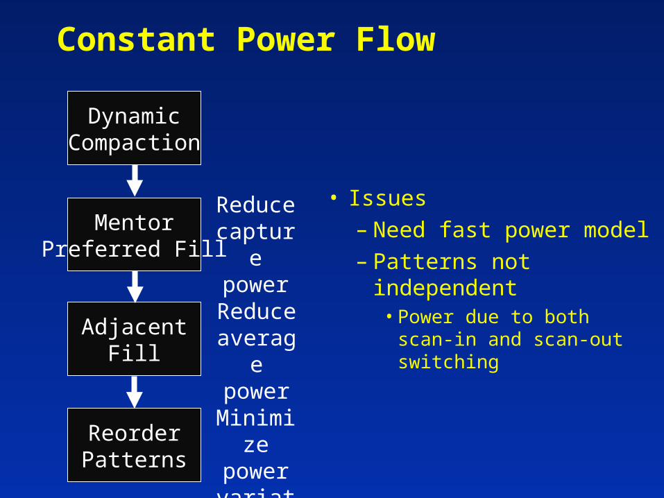
Constant Power Flow
• Issues– Need fast power model– Patterns not
independent• Power due to both scan-
in and scan-out switching
DynamicCompaction
ReorderPatterns
Minimize power
variation
AdjacentFill
Reduce average power
MentorPreferred Fill
Reduce capture power
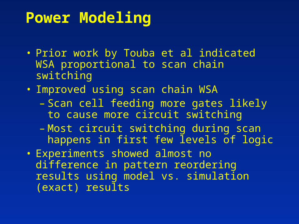
Power Modeling
• Prior work by Touba et al indicated WSA proportional to scan chain switching
• Improved using scan chain WSA– Scan cell feeding more gates likely to
cause more circuit switching– Most circuit switching during scan happens
in first few levels of logic• Experiments showed almost no difference in
pattern reordering results using model vs. simulation (exact) results
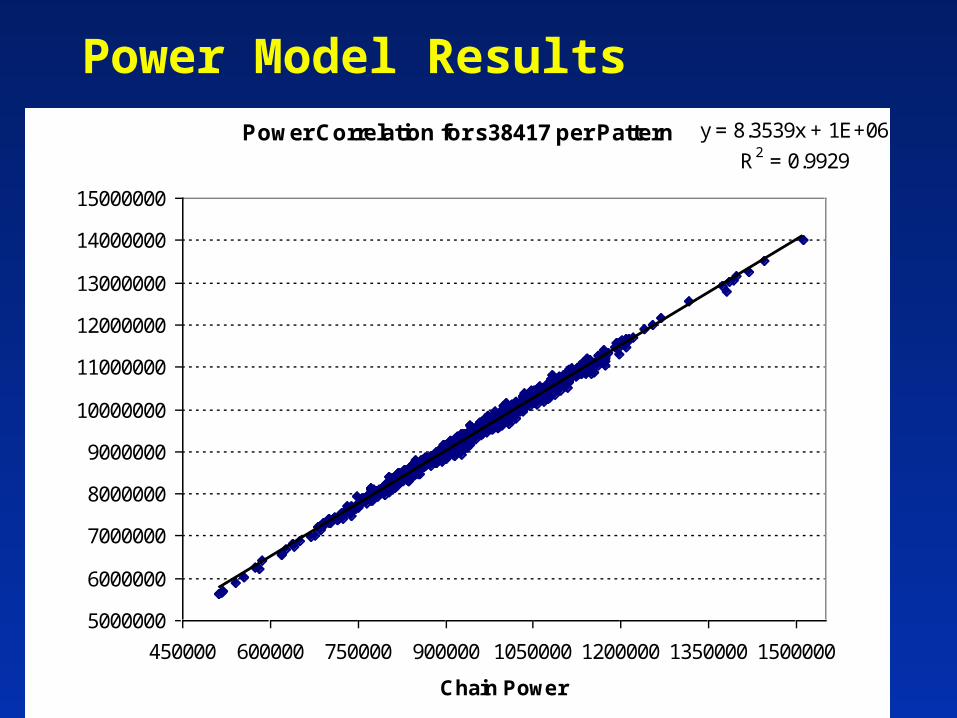
Power Model Results
Power Correlation for s38417 per Pattern y = 8.3539x + 1E+06
R2 = 0.9929
5000000
6000000
7000000
8000000
9000000
10000000
11000000
12000000
13000000
14000000
15000000
450000 600000 750000 900000 1050000 1200000 1350000 1500000
Chain Power
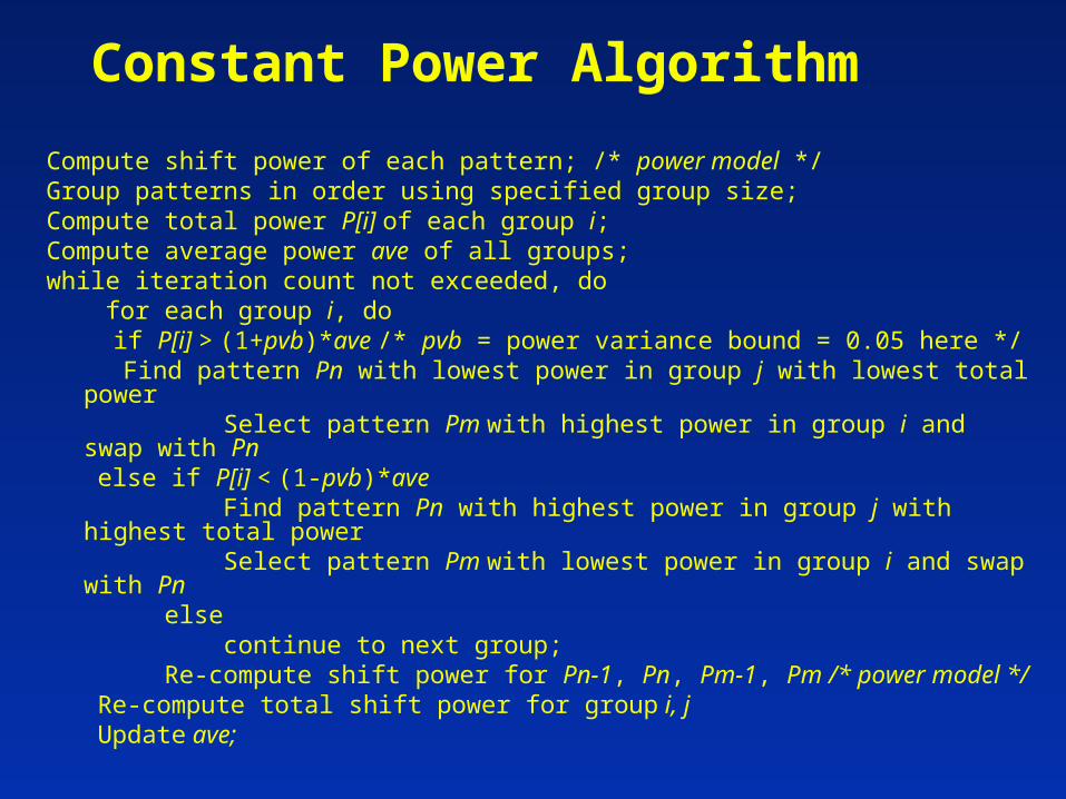
Constant Power Algorithm
Compute shift power of each pattern; /* power model */Group patterns in order using specified group size;Compute total power P[i] of each group i;Compute average power ave of all groups;while iteration count not exceeded, do for each group i, do
if P[i] > (1+pvb)*ave /* pvb = power variance bound = 0.05 here */ Find pattern Pn with lowest power in group j with lowest total power Select pattern Pm with highest power in group i and swap with Pn else if P[i] < (1-pvb)*ave Find pattern Pn with highest power in group j with highest total power Select pattern Pm with lowest power in group i and swap with Pn else continue to next group; Re-compute shift power for Pn-1, Pn, Pm-1, Pm /* power model */ Re-compute total shift power for group i, j Update ave;
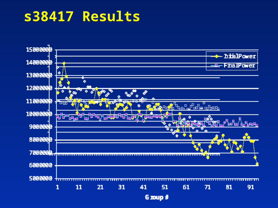
s38417 Results
Constant Power Results
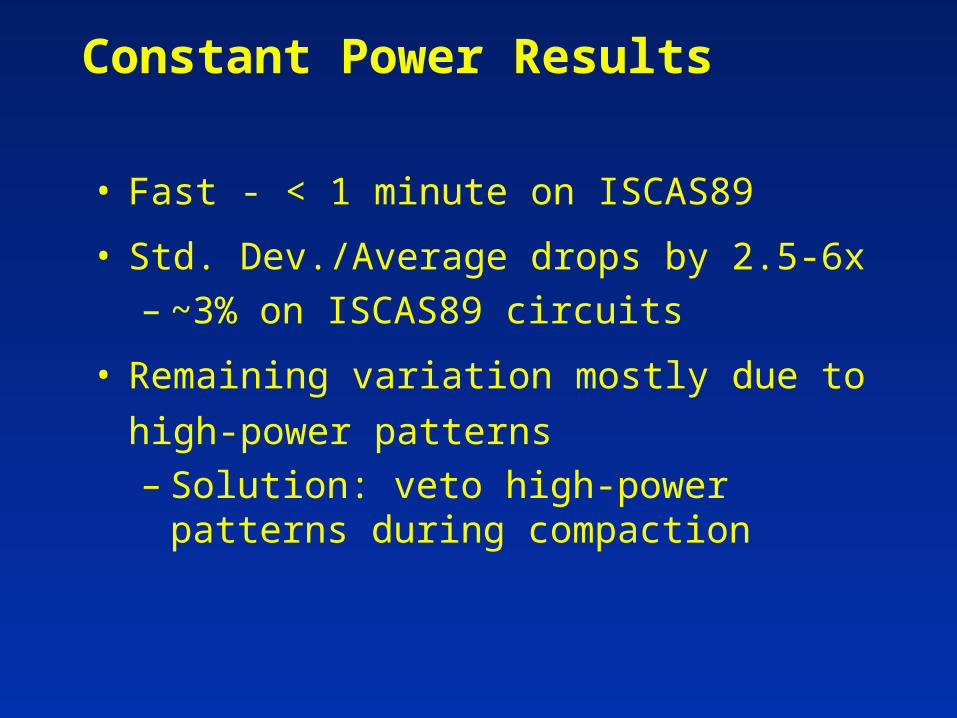
• Fast - < 1 minute on ISCAS89
• Std. Dev./Average drops by 2.5-6x– ~3% on ISCAS89 circuits
• Remaining variation mostly due to high-power
patterns– Solution: veto high-power patterns during
compaction
Conclusions
• Demonstrated KLPG on industrial designs– Modest test data volume increase– Affordable ATPG time increase
• Demonstrated noise model on industrial
design
• Demonstrated constant power reordering
Future Work
• Demonstrate on industrial data
• Fault Coverage Metric– Drop faults detected with high probability– Exploit spatial and structural correlation
• Maximize coupling capacitance
• Use supply noise model in compaction and
filling
• dI/dt model and multi-cycle launch
Acknowledgements
• Current Students– Zheng Wang– Zhongwei Jiang– Shiva Ganesan
• Former Students– Jing Wang (AMD)– Lei Wu (TI)– Wangqi Qiu (Pextra)
• Colleagues at TI, NXP
• Sponsors – NSF, SRC
Needs
• SRC task 1618 liaison
• Design and test data
More Information
– http://faculty.cs.tamu.edu/walker– http://research.cs.tamu.edu/eda– [email protected]

Questions?