Embed Size (px)
Citation preview
NOTE: This is a summary document. The complete document is available on the Atmel website at www.atmel.com.
AT91 ARM Thumb-based Microcontrollers
AT91SAM9261
Preliminary
Summary
6062LS–ATARM–23-Mar-09
Features• Incorporates the ARM926EJ-S™ ARM® Thumb® Processor
– DSP Instruction Extensions– ARM Jazelle® Technology for Java® Acceleration– 16 Kbyte Data Cache, 16 Kbyte Instruction Cache, Write Buffer– 210 MIPS at 190 MHz– Memory Management Unit– EmbeddedICE™, Debug Communication Channel Support– Mid-level implementation Embedded Trace Macrocell™
• Additional Embedded Memories– 32 Kbytes of Internal ROM, Single-cycle Access at Maximum Bus Speed– 160 Kbytes of Internal SRAM, Single-cycle Access at Maximum Processor or Bus
Speed• External Bus Interface (EBI)
– Supports SDRAM, Static Memory, NAND Flash and CompactFlash® • LCD Controller
– Supports Passive or Active Displays– Up to 16-bits per Pixel in STN Color Mode– Up to 16M Colors in TFT Mode (24-bit per Pixel), Resolution up to 2048 x 2048
• USB– USB 2.0 Full Speed (12 Mbits per second) Host Double Port
• Dual On-chip Transceivers• Integrated FIFOs and Dedicated DMA Channels
– USB 2.0 Full Speed (12 Mbits per second) Device Port• On-chip Transceiver, 2 Kbyte Configurable Integrated FIFOs
• Bus Matrix– Handles Five Masters and Five Slaves – Boot Mode Select Option– Remap Command
• Fully Featured System Controller (SYSC) for Efficient System Management, including– Reset Controller, Shutdown Controller, Four 32-bit Battery Backup Registers for a
Total of 16 Bytes– Clock Generator and Power Management Controller– Advanced Interrupt Controller and Debug Unit– Periodic Interval Timer, Watchdog Timer and Real-time Timer– Three 32-bit PIO Controllers
• Reset Controller (RSTC)– Based on Power-on Reset Cells, Reset Source Identification and Reset Output
Control• Shutdown Controller (SHDWC)
– Programmable Shutdown Pin Control and Wake-up Circuitry• Clock Generator (CKGR)
– 32,768 Hz Low-power Oscillator on Battery Backup Power Supply, Providing a Permanent Slow Clock
– 3 to 20 MHz On-chip Oscillator and two PLLs• Power Management Controller (PMC)
– Very Slow Clock Operating Mode, Software Programmable Power Optimization Capabilities
– Four Programmable External Clock Signals
• Advanced Interrupt Controller (AIC)– Individually Maskable, Eight-level Priority, Vectored Interrupt Sources– Three External Interrupt Sources and One Fast Interrupt Source, Spurious Interrupt Protected
• Debug Unit (DBGU)– 2-wire USART and support for Debug Communication Channel, Programmable ICE Access Prevention– Mode for General Purpose Two-wire UART Serial Communication
• Periodic Interval Timer (PIT)– 20-bit Interval Timer plus 12-bit Interval Counter
• Watchdog Timer (WDT)– Key Protected, Programmable Only Once, Windowed 12-bit Counter, Running at Slow Clock
• Real-Time Timer (RTT)– 32-bit Free-running Backup Counter Running at Slow Clock
• Three 32-bit Parallel Input/Output Controllers (PIO) PIOA, PIOB and PIOC– 96 Programmable I/O Lines Multiplexed with up to Two Peripheral I/Os – Input Change Interrupt Capability on Each I/O Line– Individually Programmable Open-drain, Pull-up Resistor and Synchronous Output
• Nineteen Peripheral DMA (PDC) Channels• Multimedia Card Interface (MCI)
– SDCard and MultiMediaCard™ Compliant– Automatic Protocol Control and Fast Automatic Data Transfers with PDC, MMC and SDCard Compliant
• Three Synchronous Serial Controllers (SSC)– Independent Clock and Frame Sync Signals for Each Receiver and Transmitter– I²S Analog Interface Support, Time Division Multiplex Support– High-speed Continuous Data Stream Capabilities with 32-bit Data Transfer
• Three Universal Synchronous/Asynchronous Receiver Transmitters (USART)– Individual Baud Rate Generator, IrDA® Infrared Modulation/Demodulation– Support for ISO7816 T0/T1 Smart Card, Hardware and Software Handshaking, RS485 Support
• Two Master/Slave Serial Peripheral Interface (SPI)– 8- to 16-bit Programmable Data Length, Four External Peripheral Chip Selects
• One Three-channel 16-bit Timer/Counters (TC)– Three External Clock Inputs, Two multi-purpose I/O Pins per Channel– Double PWM Generation, Capture/Waveform Mode, Up/Down Capability
• Two-wire Interface (TWI)– Master Mode Support, All Two-wire Atmel EEPROMs Supported
• IEEE® 1149.1 JTAG Boundary Scan on All Digital Pins• Required Power Supplies:
– 1.08V to 1.32V for VDDCORE and VDDBU– 3.0V to 3.6V for VDDOSC and for VDDPLL– 2.7V to 3.6V for VDDIOP (Peripheral I/Os)– 1.65V to 1.95V and 3.0V to 3.6V for VDDIOM (Memory I/Os)
• Available in a 217-ball LFBGA RoHS-compliant Package
26062LS–ATARM–23-Mar-09
AT91SAM9261 Preliminary
AT91SAM9261 Preliminary
1. DescriptionThe AT91SAM9261 is a complete system-on-chip built around the ARM926EJ-S ARM Thumbprocessor with an extended DSP instruction set and Jazelle Java accelerator. It achieves 210MIPS at 190 MHz.
The AT91SAM9261 is an optimized host processor for applications with an LCD display. Its inte-grated LCD controller supports BW and up to 16M color, active and passive LCD displays. The160 Kbyte integrated SRAM can be configured as a frame buffer minimizing the impact for LCDrefresh on the overall processor performance. The External Bus Interface incorporates control-lers for synchronous DRAM (SDRAM) and Static memories and features specific interfacecircuitry for CompactFlash and NAND Flash.
The AT91SAM9261 integrates a ROM-based Boot Loader supporting code shadowing from, forexample, external DataFlash® into external SDRAM. The software controlled Power Manage-ment Controller (PMC) keeps system power consumption to a minimum by selectivelyenabling/disabling the processor and various peripherals and adjustment of the operatingfrequency.
The AT91SAM9261 also benefits from the integration of a wide range of debug features includ-ing JTAG-ICE, a dedicated UART debug channel (DBGU) and an embedded real time trace.This enables the development and debug of all applications, especially those with real-timeconstraints.
36062LS–ATARM–23-Mar-09
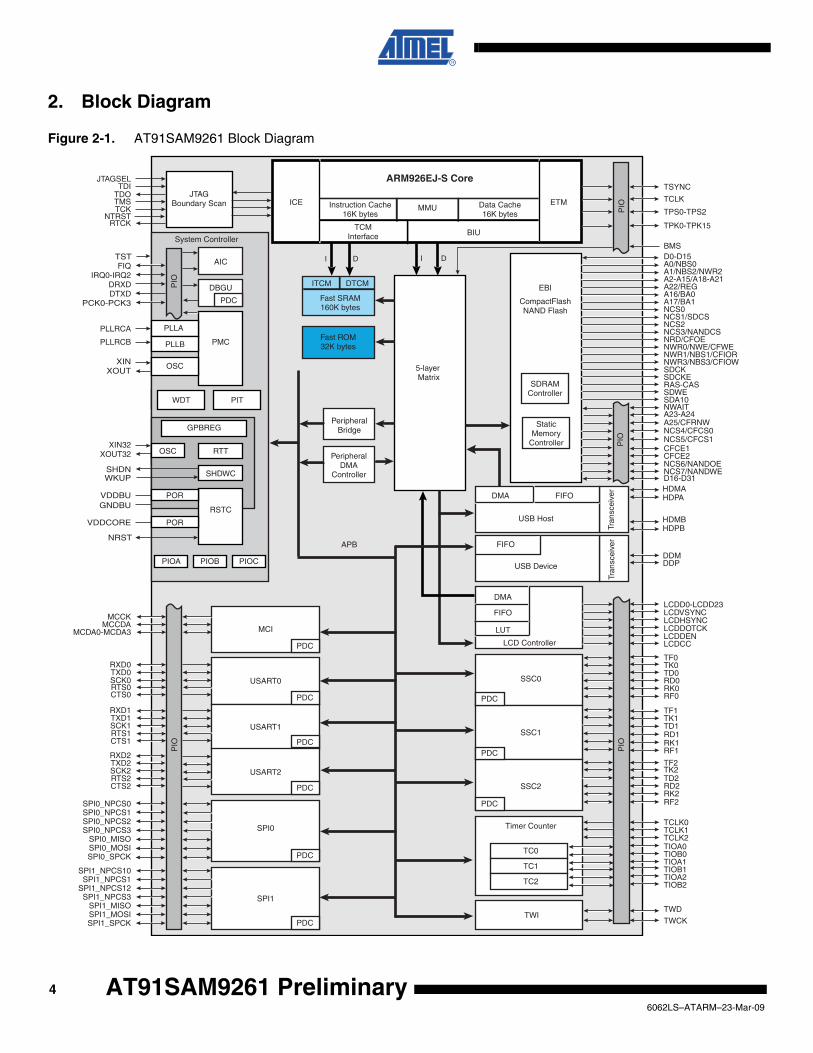
2. Block Diagram
Figure 2-1. AT91SAM9261 Block Diagram
PIO
I DI D
SSC0
SSC1
SSC2
Timer Counter
TC0
TC1
TC2
TWI
LCD Controller
DMA
FIFO
LUT
DMA FIFO
USB Host
FIFO
USB Device
ARM926EJ-S Core
JTAGBoundary Scan ICE
AIC
Fast SRAM160K bytes
PIO
Instruction Cache16K bytes
Fast ROM32K bytes
PeripheralBridge
PeripheralDMA
Controller
PLLA
PLLB
ITCM DTCM
TCMInterface
PMC
RSTC
OSC
PIOA PIOB PIOC
RTT
SHDWC
POR
OSC
WDT
GPBREG
PIT
POR
EBI
StaticMemory
Controller
PIOData Cache
16K bytesMMU
PIO
5-layer Matrix
ETM
CompactFlashNAND Flash
SDRAMController
BIU
PIO
PIO
Tran
scei
ver
Tran
scei
ver
PDC
PDC
PDC
APB
DBGU
MCI
USART0
USART1
USART2
SPI0
SPI1
PDC
PDC
PDC
PDC
PDC
PDC
PDC
System Controller
TF0TK0TD0RD0RK0RF0
TF1TK1TD1RD1RK1RF1
TF2TK2TD2RD2RK2RF2
TCLK0TCLK1TCLK2TIOA0TIOB0TIOA1TIOB1TIOA2TIOB2
TWDTWCK
LCDD0-LCDD23LCDVSYNCLCDHSYNCLCDDOTCKLCDDENLCDCC
MCCKMCCDA
MCDA0-MCDA3
RXD0TXD0SCK0RTS0CTS0
RXD1TXD1SCK1RTS1CTS1
RXD2TXD2SCK2RTS2CTS2
SPI0_NPCS0SPI0_NPCS1SPI0_NPCS2SPI0_NPCS3
SPI0_MISOSPI0_MOSISPI0_SPCK
SPI1_NPCS10SPI1_NPCS1
SPI1_NPCS12SPI1_NPCS3
SPI1_MISOSPI1_MOSISPI1_SPCK
D0-D15A0/NBS0
A2-A15/A18-A21
A16/BA0A17/BA1NCS0NCS1/SDCS
NCS3/NANDCSNRD/CFOENWR0/NWE/CFWENWR1/NBS1/CFIORNWR3/NBS3/CFIOWSDCKSDCKERAS-CASSDWESDA10
A23-A24
NCS5/CFCS1
BMS
NCS2
A25/CFRNWNCS4/CFCS0
NCS6/NANDOENCS7/NANDWE
TSYNC
TCLK
TPS0-TPS2
TPK0-TPK15
D16-D31
A1/NBS2/NWR2
NWAIT
HDMA
HDPB
HDPA
HDMB
DDMDDP
CFCE1CFCE2
JTAGSELTDI
TDO
RTCK
TMSTCK
NTRST
FIQIRQ0-IRQ2
PLLRCB
PLLRCA
DRXDDTXD
XIN32XOUT32
NRST
PCK0-PCK3
SHDNWKUP
GNDBU
XINXOUT
VDDBU
VDDCORE
TST
A22/REG
46062LS–ATARM–23-Mar-09
AT91SAM9261 Preliminary
AT91SAM9261 Preliminary
3. Signal Description
Table 3-1. Signal Description by Peripheral
Signal Name Function Type Active Level Comments
Power
VDDIOM EBI I/O Lines Power Supply Power 1.65 V to 1.95V and 3.0V to 3.6V
VDDIOP Peripherals I/O Lines Power Supply Power 2.7V to 3.6V
VDDBU Backup I/O Lines Power Supply Power 1.08V to 1.32V
VDDPLL PLL Power Supply Power 3.0V to 3.6V
VDDOSC Oscillator Power Supply Power 3.0V to 3.6V
VDDCORE Core Chip Power Supply Power 1.08V to 1.32V
GND Ground Ground
GNDPLL PLL Ground Ground
GNDOSC Oscillator Ground Ground
GNDBU Backup Ground Ground
Clocks, Oscillators and PLLs
XIN Main Oscillator Input Input
XOUT Main Oscillator Output Output
XIN32 Slow Clock Oscillator Input Input
XOUT32 Slow Clock Oscillator Output Output
PLLRCA PLL Filter Input
PLLRCB PLL Filter Input
PCK0 - PCK3 Programmable Clock Output Output
Shutdown, Wakeup Logic
SHDN Shutdown Control Output Do not tie over VDDBU.
WKUP Wake-Up Input Input Accepts between 0V and VDDBU.
ICE and JTAG
TCK Test Clock Input No pull-up resistor.
RTCK Returned Test Clock Output No pull-up resistor.
TDI Test Data In Input No pull-up resistor.
TDO Test Data Out Output
TMS Test Mode Select Input No pull-up resistor.
NTRST Test Reset Signal Input Low Pull-up resistor.
JTAGSEL JTAG Selection InputPull-down resistor. Accepts between 0V and VDDBU.
ETM™
TSYNC Trace Synchronization Signal Output
TCLK Trace Clock Output
TPS0 - TPS2 Trace ARM Pipeline Status Output
TPK0 - TPK15 Trace Packet Port Output
56062LS–ATARM–23-Mar-09
Reset/Test
NRST Microcontroller Reset I/O Low Pull-up resistor
TST Test Mode Select Input Pull-down resistor.
BMS Boot Mode Select Input
Debug Unit
DRXD Debug Receive Data Input
DTXD Debug Transmit Data Output
AIC
IRQ0 - IRQ2 External Interrupt Inputs Input
FIQ Fast Interrupt Input Input
PIO
PA0 - PA31 Parallel IO Controller A I/O Pulled-up input at reset
PB0 - PB31 Parallel IO Controller B I/O Pulled-up input at reset
PC0 - PC31 Parallel IO Controller C I/O Pulled-up input at reset
EBI
D0 - D31 Data Bus I/O Pulled-up input at reset
A0 - A25 Address Bus Output 0 at reset
NWAIT External Wait Signal Input Low
SMC
NCS0 - NCS7 Chip Select Lines Output Low
NWR0 - NWR3 Write Signal Output Low
NRD Read Signal Output Low
NWE Write Enable Output Low
NBS0 - NBS3 Byte Mask Signal Output Low
CompactFlash Support
CFCE1 - CFCE2 CompactFlash Chip Enable Output Low
CFOE CompactFlash Output Enable Output Low
CFWE CompactFlash Write Enable Output Low
CFIOR CompactFlash IO Read Output Low
CFIOW CompactFlash IO Write Output Low
CFRNW CompactFlash Read Not Write Output
CFCS0 - CFCS1 CompactFlash Chip Select Lines Output Low
NAND Flash Support
NANDOE NAND Flash Output Enable Output Low
NANDWE NAND Flash Write Enable Output Low
NANDCS NAND Flash Chip Select Output Low
Table 3-1. Signal Description by Peripheral (Continued)
Signal Name Function Type Active Level Comments
66062LS–ATARM–23-Mar-09
AT91SAM9261 Preliminary
AT91SAM9261 Preliminary
SDRAM Controller
SDCK SDRAM Clock Output
SDCKE SDRAM Clock Enable Output High
SDCS SDRAM Controller Chip Select Output Low
BA0 - BA1 Bank Select Output
SDWE SDRAM Write Enable Output Low
RAS - CAS Row and Column Signal Output Low
SDA10 SDRAM Address 10 Line Output
Multimedia Card Interface
MCCK Multimedia Card Clock Output
MCCDA Multimedia Card A Command I/O
MCDA0 - MCDA3 Multimedia Card A Data I/O
USART
SCK0 - SCK2 Serial Clock I/O
TXD0 - TXD2 Transmit Data Output
RXD0 - RXD2 Receive Data Input
RTS0 - RTS2 Request To Send Output
CTS0 - CTS2 Clear To Send Input
Synchronous Serial Controller
TD0 - TD2 Transmit Data Output
RD0 - RD2 Receive Data Input
TK0 - TK2 Transmit Clock I/O
RK0 - RK2 Receive Clock I/O
TF0 - TF2 Transmit Frame Sync I/O
RF0 - RF2 Receive Frame Sync I/O
Timer/Counter
TCLK0 - TCLK2 External Clock Input Input
TIOA0 - TIOA2 I/O Line A I/O
TIOB0 - TIOB2 I/O Line B I/O
SPI
SPI0_MISO - SPI1_MISO
Master In Slave Out I/O
SPI0_MOSI - SPI1_MOSI
Master Out Slave In I/O
SPI0_SPCK - SPI1_SPCK
SPI Serial Clock I/O
SPI0_NPCS0, SPI1_NPCS0
SPI Peripheral Chip Select 0 I/O Low
SPI0_NPCS1 - SPI0_NPCS3SPI1_NPCS1 - SPI1_NPCS3
SPI Peripheral Chip Select Output Low
Table 3-1. Signal Description by Peripheral (Continued)
Signal Name Function Type Active Level Comments
76062LS–ATARM–23-Mar-09
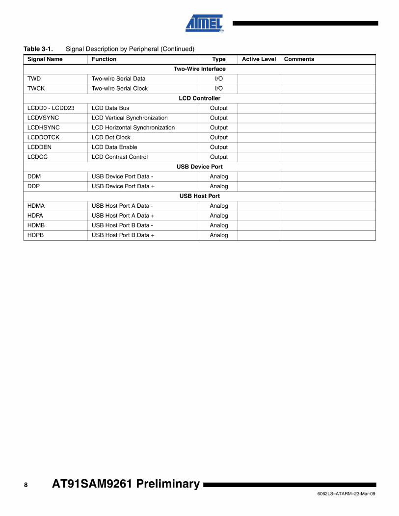
Two-Wire Interface
TWD Two-wire Serial Data I/O
TWCK Two-wire Serial Clock I/O
LCD Controller
LCDD0 - LCDD23 LCD Data Bus Output
LCDVSYNC LCD Vertical Synchronization Output
LCDHSYNC LCD Horizontal Synchronization Output
LCDDOTCK LCD Dot Clock Output
LCDDEN LCD Data Enable Output
LCDCC LCD Contrast Control Output
USB Device Port
DDM USB Device Port Data - Analog
DDP USB Device Port Data + Analog
USB Host Port
HDMA USB Host Port A Data - Analog
HDPA USB Host Port A Data + Analog
HDMB USB Host Port B Data - Analog
HDPB USB Host Port B Data + Analog
Table 3-1. Signal Description by Peripheral (Continued)
Signal Name Function Type Active Level Comments
86062LS–ATARM–23-Mar-09
AT91SAM9261 Preliminary
AT91SAM9261 Preliminary
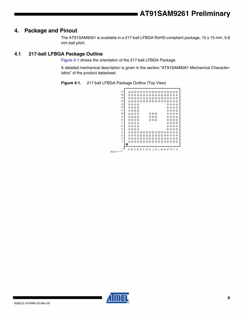
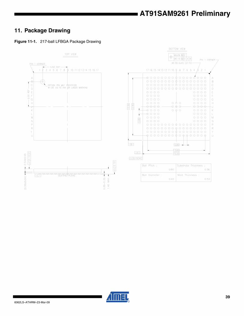
4. Package and PinoutThe AT91SAM9261 is available in a 217-ball LFBGA RoHS-compliant package, 15 x 15 mm, 0.8mm ball pitch
4.1 217-ball LFBGA Package OutlineFigure 4-1 shows the orientation of the 217-ball LFBGA Package.
A detailed mechanical description is given in the section “AT91SAM9261 Mechanical Character-istics” of the product datasheet.
Figure 4-1. 217-ball LFBGA Package Outline (Top View)
12
1234567891011
1314151617
A B C D E F G H J K L M N P R T UBall A1
96062LS–ATARM–23-Mar-09
4.2 Pinout
Note: 1. Shaded cells define the pins powered by VDDIOM.
Table 4-1. AT91SAM9261 Pinout for 217-ball LFBGA Package (1) Pin Signal Name Pin Signal Name Pin Signal Name Pin Signal Name
A1 A19 D5 VDDCORE J14 VDDIOP P17 PA20
A2 A16/BA0 D6 A10 J15 PB9 R1 PC19
A3 A14 D7 A5 J16 PB6 R2 PC21
A4 A12 D8 A0/NBS0 J17 PB4 R3 GND
A5 A9 D9 SHDN K1 D6 R4 PC27
A6 A6 D10 NC K2 D8 R5 PC29
A7 A3 D11 VDDIOP K3 D10 R6 PC4
A8 A2 D12 PB29 K4 D7 R7 PC8
A9 NC D13 PB28 K8 GND R8 PC12
A10 XOUT32 D14 PB23 K9 GND R9 PC14
A11 XIN32 D15 PB20 K10 GND R10 VDDPLL
A12 DDP D16 PB17 K14 VDDCORE R11 PA0
A13 HDPB D17 TCK K15 PB3/BMS R12 PA7
A14 HDMB E1 NWR1/NBS1/CFIOR K16 PB1 R13 PA10
A15 PB27 E2 NWR0/NWE/CFWE K17 PB2 R14 PA13
A16 GND E3 NRD/CFOE L1 D9 R15 PA17
A17 PB24 E4 SDA10 L2 D11 R16 GND
B1 A20 E14 PB22 L3 D12 R17 PA18
B2 A18 E15 PB18 L4 VDDIOM T1 PC20
B3 A15 E16 PB15 L14 PA30 T2 PC23
B4 A13 E17 TDI L15 PA27 T3 PC26
B5 A11 F1 SDCKE L16 PA31 T4 PC2
B6 A7 F2 RAS L17 PB0 T5 VDDIOP
B7 A4 F3 NWR3/NBS3/CFIOW M1 D13 T6 PC5
B8 A1/NBS2/NWR2 F4 NCS0 M2 D15 T7 PC9
B9 VDDBU F14 PB16 M3 PC18 T8 PC10
B10 JTAGSEL F15 NRST M4 VDDCORE T9 PC15
B11 WKUP F16 TDO M14 PA25 T10 VDDOSC
B12 DDM F17 NTRST M15 PA26 T11 GNDOSC
B13 PB31 G1 D0 M16 PA28 T12 PA1
B14 HDMA G2 D1 M17 PA29 T13 PA4
B15 PB26 G3 SDWE N1 D14 T14 PA6
B16 PB25 G4 NCS3/NANDCS N2 PC17 T15 PA8
B17 PB19 G14 PB14 N3 PC31 T16 PA11
C1 A22 G15 PB12 N4 VDDIOM T17 PA14
C2 A21 G16 PB11 N14 PA22 U1 PC25
C3 VDDIOM G17 PB8 N15 PA21 U2 PC0
C4 A17/BA1 H1 D2 N16 PA23 U3 PC3
C5 VDDIOM H2 D3 N17 PA24 U4 GND
C6 A8 H3 VDDIOM P1 PC16 U5 PC6
C7 GND H4 SDCK P2 PC30 U6 VDDIOP
C8 VDDIOM H8 GND P3 PC22 U7 GND
C9 GNDBU H9 GND P4 PC24 U8 PC13
C10 TST H10 GND P5 PC28 U9 PLLRCB
C11 GND H14 PB10 P6 PC1 U10 PLLRCA
C12 HDPA H15 PB13 P7 PC7 U11 XIN
C13 PB30 H16 PB7 P8 PC11 U12 XOUT
C14 NC H17 PB5 P9 GNDPLL U13 PA2
C15 VDDIOP J1 D4 P10 PA3 U14 PA5
C16 PB21 J2 D5 P11 VDDIOP U15 PA12
C17 TMS J3 GND P12 VDDCORE U16 PA9
D1 NCS2 J4 CAS P13 PA15 U17 RTCK
D2 NCS1/SDCS J8 GND P14 PA16
D3 GND J9 GND P15 VDDIOP
D4 VDDIOM J10 GND P16 PA19
106062LS–ATARM–23-Mar-09
AT91SAM9261 Preliminary
AT91SAM9261 Preliminary
5. Power Considerations
5.1 Power SuppliesThe AT91SAM9261 has six types of power supply pins:
• VDDCORE pins: Power the core, including the processor, the memories and the peripherals; voltage ranges from 1.08V and 1.32V, 1.2V nominal.
• VDDIOM pins: Power the External Bus Interface I/O lines; voltage ranges from 1.65V to 1.95V and 3.0V to 3.6V, 1.8V and 3.3V nominal.
• VDDIOP pins: Power the Peripheral I/O lines and the USB transceivers; voltage ranges from 2.7V and 3.6V, 3.3V nominal.
• VDDBU pin: Powers the Slow Clock oscillator and a part of the System Controller; voltage ranges from 1.08V and 1.32V, 1.2V nominal.
• VDDPLL pin: Powers the PLL cells; voltage ranges from 3.0V and 3.6V, 3.3V nominal.
• VDDOSC pin: Powers the Main Oscillator cells; voltage ranges from 3.0V and 3.6V, 3.3V nominal.
The double power supplies VDDIOM and VDDIOP are identified in Table 4-1 on page 10. Thesesupplies enable the user to power the device differently for interfacing with memories and forinterfacing with peripherals.
Ground pins GND are common to VDDCORE, VDDIOM and VDDIOP pins power supplies. Sep-arated ground pins are provided for VDDBU, VDDOSC and VDDPLL. The ground pins areGNDBU, GNDOSC and GNDPLL, respectively.
5.2 Power ConsumptionThe AT91SAM9261 consumes about 550 µA of static current on VDDCORE at 25°C. This staticcurrent rises at up to 5.5 mA if the temperature increases to 85°C.
On VDDBU, the current does not exceed 3 µA @25°C, but can rise at up to 20 µA @85°C.
For dynamic power consumption, the AT91SAM9261 consumes a maximum of 50 mA onVDDCORE at maximum speed in typical conditions (1.2V, 25°C), processor running full-perfor-mance algorithm.
6. I/O Line Considerations
6.1 JTAG Port PinsTMS, TDI and TCK are Schmitt trigger inputs and have no pull-up resistors.
TDO and RTCK are outputs, driven at up to VDDIOP, and have no pull-up resistor.
The JTAGSEL pin is used to select the JTAG boundary scan when asserted at a high level (tiedto VDDBU). It integrates a permanent pull-down resistor of about 15 kΩ to GNDBU, so that it canbe left unconnected for normal operations.
The NTRST pin is used to initialize the embedded ICE TAP Controller when asserted at a lowlevel. It integrates a permanent pull-up resistor of about 15 kΩ to VDDIOP, so that it can be leftunconnected for normal operations.
116062LS–ATARM–23-Mar-09
6.2 Test PinThe TST pin is used for manufacturing test purposes when asserted high. It integrates a perma-nent pull-down resistor of about 15 kΩ to GNDBU, so that it can be left unconnected for normaloperations. Driving this line at a high level leads to unpredictable results.
6.3 Reset PinNRST is an open-drain output integrating a non-programmable pull-up resistor. It can be drivenwith voltage at up to VDDIOP. As the product integrates power-on reset cells, the NRST pin canbe left unconnected in case no reset from the system needs to be applied to the product.
The NRST pin integrates a permanent pull-up resistor of 100 kΩ minimum to VDDIOP.
The NRST signal is inserted in the Boundary Scan.
6.4 PIO Controller A, B and C LinesAll the I/O lines PA0 to PA31, PB0 to PB31, and PC0 to PC31 integrate a programmable pull-upresistor of 100 kΩ. Programming of this pull-up resistor is performed independently for each I/Oline through the PIO Controllers.
After reset, all the I/O lines default as inputs with pull-up resistors enabled, except those whichare multiplexed with the External Bus Interface signals that require to be enabled as Peripheralsat reset. This is explicitly indicated in the column “Reset State” of the PIO Controller multiplexingtables.
6.5 Shutdown Logic PinsThe SHDN pin is an output only, driven by Shutdown Controller.
The pin WKUP is an input only. It can accept voltages only between 0V and VDDBU.
126062LS–ATARM–23-Mar-09
AT91SAM9261 Preliminary
AT91SAM9261 Preliminary
7. Processor and Architecture
7.1 ARM926EJ-S Processor• RISC Processor Based on ARM v5TEJ Architecture with Jazelle technology for Java
acceleration
• Two Instruction Sets
– ARM High-performance 32-bit Instruction Set
– Thumb High Code Density 16-bit Instruction Set
• DSP Instruction Extensions
• 5-Stage Pipeline Architecture:
– Instruction Fetch (F)
– Instruction Decode (D)
– Execute (E)
– Data Memory (M)
– Register Write (W)
• 16 Kbyte Data Cache, 16 Kbyte Instruction Cache
– Virtually-addressed 4-way Associative Cache
– Eight words per line
– Write-through and Write-back Operation
– Pseudo-random or Round-robin Replacement
• Write Buffer
– Main Write Buffer with 16-word Data Buffer and 4-address Buffer
– DCache Write-back Buffer with 8-word Entries and a Single Address Entry
– Software Control Drain
• Standard ARM v4 and v5 Memory Management Unit (MMU)
– Access Permission for Sections
– Access Permission for large pages and small pages can be specified separately for each quarter of the page
– 16 embedded domains
• Bus Interface Unit (BIU)
– Arbitrates and Schedules AHB Requests
– Separate Masters for both instruction and data access providing complete AHB system flexibility
– Separate Address and Data Buses for both the 32-bit instruction interface and the 32-bit data interface
– On Address and Data Buses, data can be 8-bit (Bytes), 16-bit (Half-words) or 32-bit (Words)
136062LS–ATARM–23-Mar-09
7.2 Debug and Test Features• Integrated Embedded In-circuit Emulator Real-Time
– Two real-time Watchpoint Units
– Two Independent Registers: Debug Control Register and Debug Status Register
– Test Access Port Accessible through JTAG Protocol
– Debug Communications Channel
• Debug Unit
– Two-pin UART
– Debug Communication Channel Interrupt Handling
– Chip ID Register
• Embedded Trace Macrocell: ETM9™
– Medium+ Level Implementation
– Half-rate Clock Mode
– Four Pairs of Address Comparators
– Two Data Comparators
– Eight Memory Map Decoder Inputs
– Two 16-bit Counters
– One 3-stage Sequencer
– One 45-byte FIFO
• IEEE1149.1 JTAG Boundary-scan on All Digital Pins
7.3 Bus Matrix• Five Masters and Five Slaves handled
– Handles Requests from the ARM926EJ-S, USB Host Port, LCD Controller and the Peripheral DMA Controller to internal ROM, internal SRAM, EBI, APB, LCD Controller and USB Host Port.
– Round-Robin Arbitration (three modes supported: no default master, last accessed default master, fixed default master)
– Burst Breaking with Slot Cycle Limit
• One Address Decoder Provided per Master
– Three different slaves may be assigned to each decoded memory area: one for internal boot, one for external boot, one after remap.
• Boot Mode Select Option
– Non-volatile Boot Memory can be Internal or External.
– Selection is made by BMS pin sampled at reset.
• Remap Command
– Allows Remapping of an Internal SRAM in Place of the Boot Non-Volatile Memory
– Allows Handling of Dynamic Exception Vectors
146062LS–ATARM–23-Mar-09
AT91SAM9261 Preliminary
AT91SAM9261 Preliminary
7.4 Peripheral DMA Controller• Transfers from/to peripheral to/from any memory space without intervention of the processor.
• Next Pointer Support, forbids strong real-time constraints on buffer management.
• Nineteen channels
– Two for each USART
– Two for the Debug Unit
– Two for each Serial Synchronous Controller
– Two for each Serial Peripheral Interface
– One for the Multimedia Card Interface
156062LS–ATARM–23-Mar-09
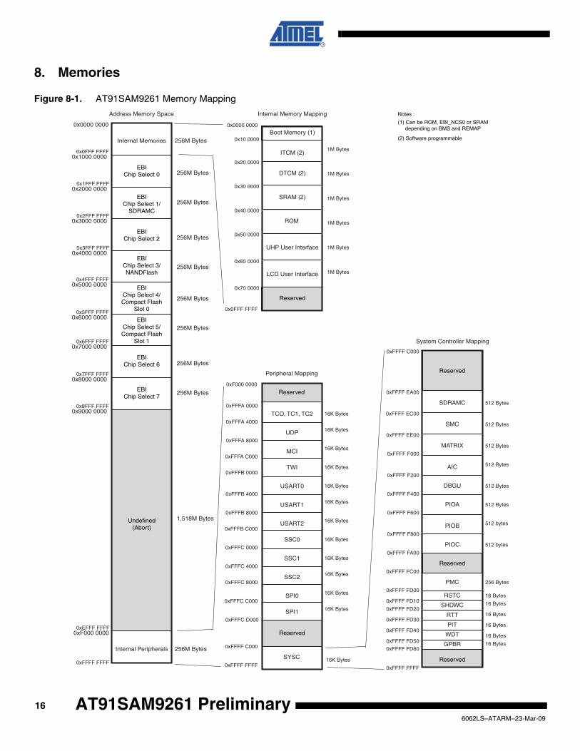
8. Memories
Figure 8-1. AT91SAM9261 Memory Mapping
16K Bytes
16K Bytes
0xFFFC 0000
16K Bytes
0xFFFC 4000
SPI1
0xFFFC C000SPI0
16K Bytes
0xFFFC 8000
16K Bytes
16K Bytes
16K Bytes
0xFFFA 4000
TCO, TC1, TC2
0xFFFA 8000
MCI
0xFFFB 0000
0xFFFB 4000
USART0
0xFFFB C000
USART1
0xFFFA 0000
0xFFFA C000
USART2
16K Bytes
TWI
16K Bytes
16K Bytes
0xFFFB 8000
16K Bytes
16K Bytes
UDP
SSC0
256M Bytes
0x1000 0000
0x0000 0000
0x0FFF FFFF
0xFFFF FFFF
0xF000 00000xEFFF FFFF
Address Memory Space
Internal Peripherals
Internal Memories
EBIChip Select 0
EBIChip Select 1/
SDRAMC
EBIChip Select 2
EBIChip Select 3/NANDFlash
EBIChip Select 4/Compact Flash
Slot 0
EBIChip Select 5/Compact Flash
Slot 1
EBIChip Select 6
EBIChip Select 7
Undefined(Abort)
256M Bytes
256M Bytes
256M Bytes
256M Bytes
256M Bytes
256M Bytes
256M Bytes
1,518M Bytes
0x2000 00000x1FFF FFFF
0x3000 00000x2FFF FFFF
0x4000 00000x3FFF FFFF
0x6FFF FFFF
0x6000 00000x5FFF FFFF
0x5000 00000x4FFF FFFF
0x7000 0000
0x7FFF FFFF0x8000 0000
0x8FFF FFFF0x9000 0000
256M Bytes
0xFFFF FD00
0xFFFF FC00
0xFFFF FA00
0xFFFF F800
0xFFFF F600
0xFFFF F400
0xFFFF F200
16 Bytes
256 Bytes
512 bytes
512 bytes
512 Bytes
512 Bytes
PMC
PIOC
PIOB
PIOA
DBGU
RSTC
0xFFFF F000
512 BytesAIC
0xFFFF EE00
512 BytesMATRIX
0xFFFF EC00
512 BytesSMC
0xFFFF FD10 16 BytesSHDWC
0xFFFF EA00
512 BytesSDRAMC
0xFFFF FD2016 BytesRTT
0xFFFF FD3016 BytesPIT
0xFFFF FD4016 BytesWDT
0xFFFF FD50 16 BytesGPBR0xFFFF FD60
Reserved
Reserved
256M Bytes
1M BytesITCM (2)
0x20 0000
DTCM (2)
0x30 0000
SRAM (2)
0x10 0000
UHP User Interface
0x50 0000
Reserved
0x0FFF FFFF
Peripheral Mapping
Internal Memory Mapping
Boot Memory (1)0x0000 0000 (1) Can be ROM, EBI_NCS0 or SRAM
depending on BMS and REMAP
Notes :
LCD User Interface
0x60 0000
(2) Software programmable
SSC1
SSC2
0xFFFC D000
0xFFFF C000
SYSC Reserved0xFFFF FFFF
System Controller Mapping
16K Bytes
0xFFFF FFFF
Reserved
0xFFFF C000
0x70 0000
1M Bytes
1M Bytes
1M Bytes
1M Bytes
Reserved0xF000 0000
0x40 0000
ROM 1M Bytes
166062LS–ATARM–23-Mar-09
AT91SAM9261 Preliminary
AT91SAM9261 Preliminary
A first level of address decoding is performed by the Bus Matrix, i.e., the implementation of theAdvanced High performance Bus (AHB) for its Master and Slave interfaces with additionalfeatures.
Decoding breaks up the 4 Gbytes of address space into 16 areas of 256 Mbytes. The areas 1 to8 are directed to the EBI that associates these areas to the external chip selects NCS0 to NCS7.The area 0 is reserved for the addressing of the internal memories, and a second level of decod-ing provides 1 Mbyte of internal memory area. The area 15 is reserved for the peripherals andprovides access to the Advanced Peripheral Bus (APB).
Other areas are unused and performing an access within them provides an abort to the masterrequesting such an access.
The Bus Matrix manages five Masters and five Slaves.
Each Master has its own bus and its own decoder, thus allowing a different memory mappingper Master.
Regarding Master 0 and Master 1 (ARM926™ Instruction and Data), three different Slaves areassigned to the memory space decoded at address 0x0: one for internal boot, one for externalboot, one after remap. Refer to Table 8-3 for details.
Each Slave has its own arbiter, thus allowing a different arbitration per Slave.
8.1 Embedded Memories • 32 KB ROM
– Single Cycle Access at full bus speed
• 160 KB Fast SRAM
– Single Cycle Access at full bus speed
– Supports ARM926EJ-S TCM interface at full processor speed
Table 8-1. List of Bus Matrix Masters
Master 0 ARM926 Instruction
Master 1 ARM926 Data
Master 2 PDC
Master 3 LCD Controller
Master 4 USB Host
Table 8-2. List of Bus Matrix Slaves
Slave 0 Internal SRAM
Slave 1 Internal ROM
Slave 2 LCD Controller and USB Host Port Interfaces
Slave 3 External Bus Interface
Slave 4 Internal Peripherals
176062LS–ATARM–23-Mar-09
8.1.1 Internal Memory Mapping Table 8-3 summarizes the Internal Memory Mapping for each Master, depending on the Remapstatus and the BMS state at reset.
Note: 1. EBI NCS0 is to be connected to a 16-bit non-volatile memory. The access configuration is defined by the reset state of SMC Setup, SMC Pulse, SMC Cycle and SMC Mode CS0 registers.
8.1.1.1 Internal SRAMThe AT91SAM9261 embeds a high-speed 160 Kbyte SRAM. This Internal SRAM is split intothree areas. Its Memory Mapping is detailed in Table 8-3 above.
• Internal SRAM A is the ARM926EJ-S Instruction TCM and the user can map this SRAM block anywhere in the ARM926 instruction memory space using CP15 instructions. This SRAM block is also accessible by the ARM926 Data Master and by the AHB Masters through the AHB bus at address 0x0010 0000.
• Internal SRAM B is the ARM926EJ-S Data TCM and the user can map this SRAM block anywhere in the ARM926 data memory space using CP15 instructions. This SRAM block is also accessible by the ARM926 Data Master and by the AHB Masters through the AHB bus at address 0x0020 0000.
• Internal SRAM C is only accessible by all the AHB Masters.After reset and until the Remap Command is performed, this SRAM block is accessible through the AHB bus at address 0x0030 0000 by all the AHB Masters.After Remap, this SRAM block also becomes accessible through the AHB bus at address 0x0 by the ARM926 Instruction and the ARM926 Data Masters.
Within the 160 Kbyte SRAM size available, the amount of memory assigned to each block issoftware programmable as a multiple of 16 Kbytes according to Table 8-4. This table providesthe size of the Internal SRAM C according to the size of the Internal SRAM A and the InternalSRAM B.
Note that among the ten 16 Kbyte blocks making up the Internal SRAM, two are permanentlyassigned to Internal SRAM C.
At reset, the whole memory (160 Kbytes) is assigned to Internal SRAM C.
Table 8-3. Internal Memory Mapping
Address Master 0: ARM926 Instruction Master 1: ARM926 Data
REMAP(RCB0) = 0 REMAP (RCB0) = 1 REMAP (RCB1) = 0 REMAP (RCB1) = 1
BMS = 1 BMS = 0 BMS = 1 BMS = 0
0x0000 0000 Int. ROM EBI NCS0(1) Int. RAM C Int. ROM EBI NCS0(1) Int. RAM C
Table 8-4. Internal SRAM Block Size
Internal SRAM C
Internal SRAM A (ITCM)
0 16 Kbytes 32 Kbytes 64 Kbytes
Internal SRAM B (DCTM)
0 160 Kbytes 144 Kbytes 128 Kbytes 96 Kbytes
16 Kbytes 144 Kbytes 128 Kbytes 112 Kbytes 80 Kbytes
32 Kbytes 128 Kbytes 112 Kbytes 96 Kbytes 64 Kbytes
64 Kbytes 96 Kbytes 80 Kbytes 64 Kbytes 32 Kbytes
186062LS–ATARM–23-Mar-09
AT91SAM9261 Preliminary
AT91SAM9261 Preliminary
The memory blocks assigned to SRAM A, SRAM B and SRAM C areas are not contiguous andwhen the user dynamically changes the Internal SRAM configuration, the new 16 Kbyte blockorganization may affect the previous configuration from a software point of view.
Table 8-5 illustrates different configurations and the related 16 Kbyte blocks (RB0 to RB9)assignments.
Note: 1. Configuration after reset.
8.1.1.2 Internal ROMThe AT91SAM9261 integrates a 32 Kbyte Internal ROM mapped at address 0x0040 0000. It isalso accessible at address 0x0 after reset and before remap if the BMS is tied high during reset.
8.1.1.3 USB Host PortThe AT91SAM9261 integrates a USB Host Port Open Host Controller Interface (OHCI). The reg-isters of this interface are directly accessible on the AHB Bus and are mapped like a standardinternal memory at address 0x0050 0000.
8.1.1.4 LCD ControllerThe AT91SAM9261 integrates an LCD Controller. The interface is directly accessible on theAHB Bus and is mapped like a standard internal memory at address 0x0060 0000.
Table 8-5. 16 Kbyte Block Allocation
Decoded Area Address
Configuration Examples and Related 16 Kbyte Block Assignments
ITCM = 0 KbyteDTCM = 0 KbyteAHB = 160 Kbytes (1)
ITCM = 64 KbytesDTCM = 64 KbytesAHB = 32 Kbytes
ITCM = 32 KbytesDTCM = 64 KbytesAHB = 64 Kbytes
ITCM = 32 KbytesDTCM = 16 KbytesAHB = 112 Kbytes
InternalSRAM A(ITCM)
0x0010 0000 RB3 RB3 RB3
0x0010 4000 RB2 RB2 RB2
0x0010 8000 RB1
0x0010 C000 RB0
InternalSRAM B(DTCM)
0x0020 0000 RB7 RB7 RB7
0x0020 4000 RB6 RB6
0x0020 8000 RB5 RB5
0x0020 C000 RB4 RB4
InternalSRAM C
(AHB)
0x0030 0000 RB9 RB9 RB9 RB9
0x0030 4000 RB8 RB8 RB8 RB8
0x0030 8000 RB7 RB1 RB6
0x0030 C000 RB6 RB0 RB5
0x0031 0000 RB5 RB4
0x0031 4000 RB4 RB1
0x0031 8000 RB3 RB0
0x0031 C000 RB2
0x0032 0000 RB1
0x0032 4000 RB0
196062LS–ATARM–23-Mar-09
8.1.2 Boot StrategiesThe system always boots at address 0x0. To ensure a maximum number of possibilities for boot,the memory layout can be configured with two parameters.
REMAP allows the user to lay out the first internal SRAM bank to 0x0 to ease development. Thisis done by software once the system has booted for each Master of the Bus Matrix. Refer to theBus Matrix Section for more details.
When REMAP = 0, BMS allows the user to lay out to 0x0, at his convenience, the ROM or anexternal memory. This is done via hardware at reset.
Note: Memory blocks not affected by these parameters can always be seen at their specified base addresses. See the complete memory map presented in Figure 8-1 on page 16.
The AT91SAM9261 Bus Matrix manages a boot memory that depends on the level on the BMSpin at reset. The internal memory area mapped between address 0x0 and 0x000F FFFF isreserved for this purpose.
If BMS is detected at 1, the boot memory is the embedded ROM.
If BMS is detected at 0, the boot memory is the memory connected on the Chip Select 0 of theExternal Bus Interface.
8.1.2.1 BMS = 1, Boot on Embedded ROMThe system boots using the Boot Program.
• Downloads and runs an application from external storage media into internal SRAM
• Downloaded code size depends on embedded SRAM size
• Automatic detection of valid application
• Bootloader on a non-volatile memory
– SDCard
– NAND Flash
– SPI DataFlash connected on NPCS0 of the SPI
• SAM-BA® boot in case no valid program is detected in external NVM, supporting:
– Serial communication on a DBGU
– USB Device HS Port
8.1.2.2 BMS = 0, Boot on External Memory
• Boot on slow clock (32,768 Hz)
• Boot with the default configuration for the Static Memory Controller, byte select mode, 16-bit data bus, Read/Write controlled by Chip Select, allows boot on 16-bit non-volatile memory.
The customer-programmed software must perform a complete configuration.
To speed up the boot sequence when booting at 32 kHz EBI CS0 (BMS=0), the user must takethe following steps:
1. Program the PMC (main oscillator enable or bypass mode).2. Program and start the PLL.3. Reprogram the SMC setup, cycle, hold, mode timings registers for CS0 to adapt them
to the new clock4. Switch the main clock to the new value.
206062LS–ATARM–23-Mar-09
AT91SAM9261 Preliminary
AT91SAM9261 Preliminary
8.1.3 ETM™ MemoriesThe eight ETM9 Medium+ memory map decoder inputs are connected to custom addressdecoders and the resulting memory mapping is summarized in Table 8-6.
8.2 External MemoriesThe external memories are accessed through the External Bus Interface (Bus Matrix Slave 3).
Refer to the memory map in Figure 8-1 on page 16.
Table 8-6. ETM9 Memory Mapping
Product Resource Area Access Type Start Address End Address
SRAM Internal Data 0x0000 0000 0x002F FFFF
SRAM Internal Fetch 0x0000 0000 0x002F FFFF
ROM Internal Data 0x0040 0000 0x004F FFFF
ROM Internal Fetch 0x0040 0000 0x004F FFFF
External Bus Interface External Data 0x1000 0000 0x8FFF FFFF
External Bus Interface External Fetch 0x1000 0000 0x8FFF FFFF
User Peripherals Internal Data 0xF000 0000 0xFFFF BFFF
System Peripherals Internal Data 0xFFFF C000 0xFFFF FFFF
216062LS–ATARM–23-Mar-09
9. System ControllerThe System Controller manages all vital blocks of the microcontroller: interrupts, clocks, power,time, debug and reset.
The System Peripherals are all mapped within the highest 6 Kbytes of address space, betweenaddresses 0xFFFF EA00 and 0xFFFF FFFF. Each peripheral has an address space of 256 or512 Bytes, representing 64 or 128 registers.
Figure 9-1 on page 23 shows the System Controller block diagram.
Figure 8-1 on page 16 shows the mapping of the User Interfaces of the System Controllerperipherals.
226062LS–ATARM–23-Mar-09
AT91SAM9261 Preliminary
AT91SAM9261 Preliminary
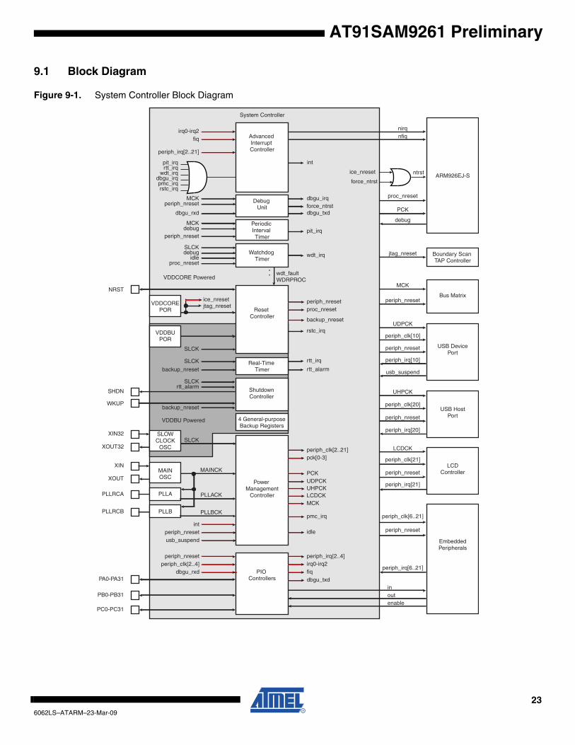
9.1 Block Diagram
Figure 9-1. System Controller Block Diagram
NRST
SLCK
Advanced Interrupt Controller
Real-Time Timer
Periodic Interval Timer
Reset Controller
PA0-PA31
periph_nreset
System Controller
Watchdog Timer
wdt_faultWDRPROC
PIO Controllers
Power Management
Controller
XIN
XOUT
PLLRCA
MAINCK
PLLACK
pit_irqMCK
proc_nreset
wdt_irq
periph_irq{2..4]periph_nreset
periph_clk[2..21]
PCK
MCK
pmc_irq
UDPCK
nirqnfiq
rtt_irq
EmbeddedPeripherals
periph_clk[2..4]
pck[0-3]
inoutenable
ARM926EJ-S
SLCK
SLCK
irq0-irq2fiq
irq0-irq2fiq
periph_irq[6..21]
periph_irq[2..21]
int
intperiph_nreset
periph_clk[6..21]
jtag_nreset
ice_nreset
proc_nreset
periph_nreset
dbgu_txddbgu_rxd
pit_irqrtt_irq
dbgu_irqpmc_irq
rstc_irq
wdt_irq
rstc_irq
SLCK
Boundary Scan TAP Controller
jtag_nreset
debug
PCK
debugidle
debug
Bus Matrix
MCK
periph_nreset
proc_nreset
backup_nreset
periph_nreset
idle
Debug Unit
dbgu_irqMCK
dbgu_rxd
periph_nreset force_ntrstdbgu_txd
USB DevicePort
UDPCK
periph_nreset
periph_clk[10]
periph_irq[10]
usb_suspend
usb_suspendrtt_alarm
ShutdownController
SLCKrtt_alarm
backup_nreset
SHDN
WKUP
4 General-purposeBackup Registers
backup_nreset
XIN32
XOUT32
LCDCK
PLLRCB PLLBCK
UHPCK
PB0-PB31
PC0-PC31
USB HostPort
UHPCK
periph_nreset
periph_clk[20]
periph_irq[20]
LCDController
LCDCK
periph_nreset
periph_clk[21]
periph_irq[21]
VDDBU Powered
VDDCORE Powered
force_ntrst
ntrst
VDDCOREPOR
MAINOSC
PLLA
VDDBUPOR
SLOWCLOCK
OSC
PLLB
ice_nreset
236062LS–ATARM–23-Mar-09
9.2 Reset Controller• Based on two Power-on-Reset cells
• Status of the last reset
– Either cold reset, first reset, soft reset, user reset, watchdog reset, wake-up reset
• Controls the internal resets and the NRST pin output
9.3 Shutdown Controller• Shutdown and Wake-up logic:
– Software programmable assertion of the SHDN pin
– Deassertion Programmable on a WKUP pin level change or on alarm
9.4 General-purpose Backup Registers• Four 32-bit general-purpose backup registers
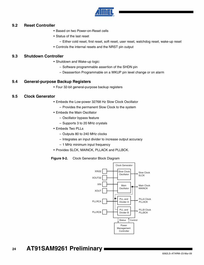
9.5 Clock Generator• Embeds the Low-power 32768 Hz Slow Clock Oscillator
– Provides the permanent Slow Clock to the system
• Embeds the Main Oscillator
– Oscillator bypass feature
– Supports 3 to 20 MHz crystals
• Embeds Two PLLs
– Outputs 80 to 240 MHz clocks
– Integrates an input divider to increase output accuracy
– 1 MHz minimum input frequency
• Provides SLCK, MAINCK, PLLACK and PLLBCK.
Figure 9-2. Clock Generator Block Diagram
Power Management
Controller
XIN
XOUT
PLLRCA
Slow Clock SLCK
Main ClockMAINCK
PLLA ClockPLLACK
ControlStatus
PLL and Divider BPLLRCB
PLLB ClockPLLBCK
XIN32
XOUT32
Slow ClockOscillator
Main Oscillator
PLL and Divider A
Clock Generator
246062LS–ATARM–23-Mar-09
AT91SAM9261 Preliminary
AT91SAM9261 Preliminary
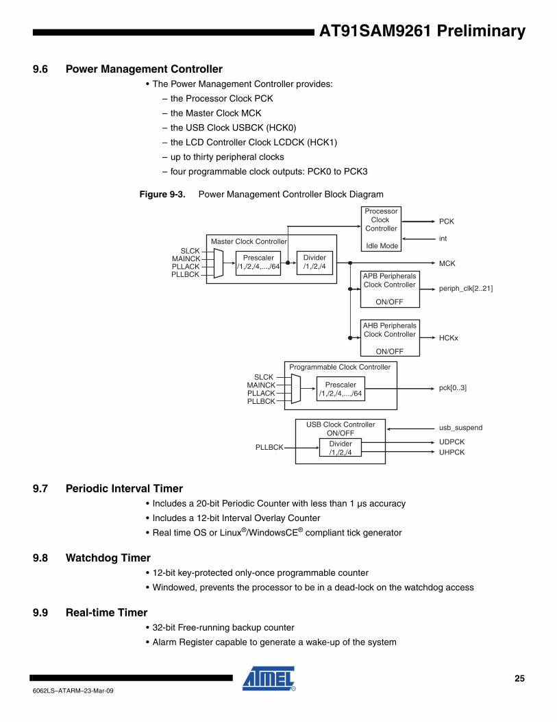
9.6 Power Management Controller• The Power Management Controller provides:
– the Processor Clock PCK
– the Master Clock MCK
– the USB Clock USBCK (HCK0)
– the LCD Controller Clock LCDCK (HCK1)
– up to thirty peripheral clocks
– four programmable clock outputs: PCK0 to PCK3
Figure 9-3. Power Management Controller Block Diagram
9.7 Periodic Interval Timer• Includes a 20-bit Periodic Counter with less than 1 µs accuracy
• Includes a 12-bit Interval Overlay Counter
• Real time OS or Linux®/WindowsCE® compliant tick generator
9.8 Watchdog Timer• 12-bit key-protected only-once programmable counter
• Windowed, prevents the processor to be in a dead-lock on the watchdog access
9.9 Real-time Timer• 32-bit Free-running backup counter
• Alarm Register capable to generate a wake-up of the system
MCK
periph_clk[2..21]
int
UDPCK
usb_suspend
SLCKMAINCKPLLACK
Prescaler/1,/2,/4,...,/64
PCKProcessor
Clock Controller
Idle ModeMaster Clock Controller
APB PeripheralsClock Controller
ON/OFF
USB Clock ControllerON/OFF
SLCKMAINCKPLLACK
Prescaler/1,/2,/4,...,/64
Programmable Clock Controller
PLLBCK Divider/1,/2,/4
pck[0..3]
PLLBCK
PLLBCK
UHPCK
Divider/1,/2,/4
HCKx
AHB PeripheralsClock Controller
ON/OFF
256062LS–ATARM–23-Mar-09
9.10 Advanced Interrupt Controller• Controls the interrupt lines (nIRQ and nFIQ) of an ARM Processor
• Thirty-two individually maskable and vectored interrupt sources
– Source 0 is reserved for the Fast Interrupt Input (FIQ)
– Source 1 is reserved for system peripherals (PIT, RTT, PMC, DBGU, etc.)
– Source 2 to Source 31 control up to thirty embedded peripheral interrupts or external interrupts
– Programmable edge-triggered or level-sensitive internal sources
– Programmable positive/negative edge-triggered or high/low level-sensitive
• Four External Sources
• 8-level Priority Controller
– Drives the normal interrupt of the processor
– Handles priority of the interrupt sources 1 to 31
– Higher priority interrupts can be served during service of lower priority interrupt
• Vectoring
– Optimizes Interrupt Service Routine Branch and Execution
– One 32-bit Vector Register per interrupt source
– Interrupt Vector Register reads the corresponding current Interrupt Vector
• Protect Mode
– Easy debugging by preventing automatic operations when protect mode is enabled
• Fast Forcing
– Permits redirecting any normal interrupt source on the Fast Interrupt of the processor
• General Interrupt Mask
– Provides processor synchronization on events without triggering an interrupt
9.11 Debug Unit• Composed of four functions
– Two-pin UART
– Debug Communication Channel (DCC) support
– Chip ID Registers
– ICE Access Prevention
• Two-pin UART
– Implemented features are 100% compatible with the standard Atmel USART
– Independent receiver and transmitter with a common programmable Baud Rate Generator
– Even, Odd, Mark or Space Parity Generation
– Parity, Framing and Overrun Error Detection
– Automatic Echo, Local Loopback and Remote Loopback Channel Modes
– Support for two PDC channels with connection to receiver and transmitter
• Debug Communication Channel Support
266062LS–ATARM–23-Mar-09
AT91SAM9261 Preliminary
AT91SAM9261 Preliminary
– Offers visibility of COMMRX and COMMTX signals from the ARM Processor
• Chip ID Registers
– Identification of the device revision, sizes of the embedded memories, set of peripherals
• ICE Access prevention
– Enables software to prevent system access through the ARM Processor’s ICE
– Prevention is made by asserting the NTRST line of the ARM Processor’s ICE
9.12 PIO Controllers• Three PIO Controllers, each controlling up to 32 programmable I/O Lines
– PIOA has 32 I/O Lines
– PIOB has 32 I/O Lines
– PIOC has 32 I/O Lines
• Fully programmable through Set/Clear Registers
• Multiplexing of two peripheral functions per I/O Line
• For each I/O Line (whether assigned to a peripheral or used as general-purpose I/O)
– Input change interrupt
– Glitch filter
– Multi-drive option enables driving in open drain
– Programmable pull up on each I/O line
– Pin data status register, supplies visibility of the level on the pin at any time
• Synchronous output, provides Set and Clear of several I/O lines in a single write
276062LS–ATARM–23-Mar-09
10. Peripherals
10.1 User InterfaceThe User Peripherals are mapped in the upper 256 Mbytes of the address space between theaddresses 0xFFFA 0000 and 0xFFFC FFFF. Each User Peripheral is allocated 16 Kbytes ofaddress space.
A complete memory map is presented in Figure 8-1 on page 16.
10.2 Peripheral IdentifiersTable 10-1 defines the Peripheral Identifiers of the AT91SAM9261. A peripheral identifier isrequired for the control of the peripheral interrupt with the Advanced Interrupt Controller and forthe control of the peripheral clock with the Power Management Controller.
Note: Setting AIC, SYSIRQ, UHP, LCDC and IRQ0 to IRQ2 bits in the clock set/clear registers of the PMC has no effect.
Table 10-1. Peripheral Identifiers
Peripheral ID Peripheral Mnemonic Peripheral Name External Interrupt
0 AIC Advanced Interrupt Controller FIQ
1 SYSIRQ System Interrupt
2 PIOA Parallel I/O Controller A
3 PIOB Parallel I/O Controller B
4 PIOC Parallel I/O Controller C
5 - Reserved
6 US0 USART 0
7 US1 USART 1
8 US2 USART 2
9 MCI Multimedia Card Interface
10 UDP USB Device Port
11 TWI Two-Wire Interface
12 SPI0 Serial Peripheral Interface 0
13 SPI1 Serial Peripheral Interface 1
14 SSC0 Synchronous Serial Controller 0
15 SSC1 Synchronous Serial Controller 1
16 SSC2 Synchronous Serial Controller 2
17 TC0 Timer/Counter 0
18 TC1 Timer/Counter 1
19 TC2 Timer/Counter 2
20 UHP USB Host Port
21 LCDC LCD Controller
22 - 28 - Reserved
29 AIC Advanced Interrupt Controller IRQ0
30 AIC Advanced Interrupt Controller IRQ1
31 AIC Advanced Interrupt Controller IRQ2
286062LS–ATARM–23-Mar-09
AT91SAM9261 Preliminary
AT91SAM9261 Preliminary
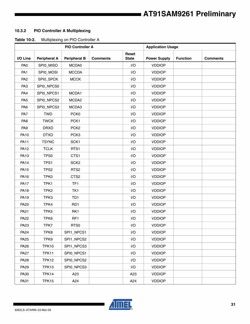
10.3 Peripheral Multiplexing on PIO LinesThe AT91SAM9261 features three PIO controllers, PIOA, PIOB and PIOC, that multiplex the I/Olines of the peripheral set.
Each PIO Controller controls up to thirty-two lines. Each line can be assigned to one of twoperipheral functions, A or B. Table 10-2 on page 31, Table 10-3 on page 32 and Table 10-4 onpage 33 define how the I/O lines of the peripherals A and B are multiplexed on the PIO Control-lers. The two columns “Function” and “Comments” have been inserted for the user’s owncomments; they may be used to track how pins are defined in an application.
Note that some output only peripheral functions might be duplicated within the tables.
The column “Reset State” indicates whether the PIO line resets in I/O mode or in peripheralmode. If I/O is mentioned, the PIO line resets in input with the pull-up enabled, so that the deviceis maintained in a static state as soon as the reset is released. As a result, the bit correspondingto the PIO line in the register PIO_PSR (Peripheral Status Register) resets low.
If a signal name is mentioned in the “Reset State” column, the PIO line is assigned to this func-tion and the corresponding bit in PIO_PSR resets high. This is the case of pins controllingmemories, in particular the address lines, which require the pin to be driven as soon as the resetis released. Note that the pull-up resistor is also enabled in this case.
10.3.1 Resource Multiplexing
10.3.1.1 LCD ControllerThe LCD Controller can interface with several LCD panels. It supports 4, 8 or 16 bit-per-pixelwithout any limitation. Interfacing 24 bit-per-pixel TFTs panel prevents using the SSC0 and thechip select line 0 of the SPI1.
16 bit-per-pixel TFT panels are interfaced through peripheral B functions, as color data is outputon LCDD3 to LCDD7, LCDD11 to LCDD15 and LCDD19 to LCDD23. Intensity bit is output onLCDD2, LCDD10 and LCDD18. Using the peripheral B does not prevent using the SSC0 andthe SPI1 lines.
10.3.1.2 ETMUsing the ETM prevents:
• using the USART1 and USART2 control signals, in particular the SCK lines which are required to use the USART as ISO7816 and the RTS and CTS to handle hardware handshaking on the serial lines. In case the ETM and an ISO7816 connection are both required, the USART0 has to be used as a Smart Card interface.
• using the SSC1
• addressing a static memory of more than 8 Mbytes, which requires the A23 and A24 address lines
• using the chip select lines 1 to 3 of SPI0 and SPI1
10.3.1.3 EBIIf not required, the NWAIT function (external wait request) can be deactivated by software,allowing this pin to be used as a PIO.
10.3.1.4 32-bit Data BusUsing a 32-bit Data Bus prevents:
296062LS–ATARM–23-Mar-09
• using the three Timer Counter channels’ outputs and trigger inputs
• using the SSC2
10.3.1.5 NAND Flash InterfaceUsing the NAND Flash interface prevents:
• using NCS3, NCS6 and NCS7 to access other parallel devices
10.3.1.6 Compact Flash InterfaceUsing the CompactFlash interface prevents:
• using NCS4 and/or NCS5 to access other parallel devices
10.3.1.7 SPI0 and the MultiMedia Card InterfaceAs the DataFlash Card is compatible with the SDCard, it is useful to multiplex SPI and MCI.Here, the SPI0 signal is multiplexed with the MCI.
10.3.1.8 USARTs
• Using the USART1 and USART2 control signals prevents using the ETM.
• Alternatively, using USART0 with its control signals prevents using some clock outputs and interrupt lines.
10.3.1.9 Clock Outputs
• Using the clock outputs multiplexed with the PIO A prevents using the Debug Unit and/or the Two Wire Interface.
• Alternatively, using the second implementation of the clock outputs prevents using the LCD Controller Interface and/or USART0.
10.3.1.10 Interrupt Lines
• Using FIQ prevents using the USART0 control signals.
• Using IRQ0 prevents using the NWAIT EBI signal.
• Using the IRQ1 and/or IRQ2 prevents using the SPI1.
306062LS–ATARM–23-Mar-09
AT91SAM9261 Preliminary
AT91SAM9261 Preliminary
10.3.2 PIO Controller A Multiplexing
Table 10-2. Multiplexing on PIO Controller A
PIO Controller A Application Usage
I/O Line Peripheral A Peripheral B CommentsReset State Power Supply Function Comments
PA0 SPI0_MISO MCDA0 I/O VDDIOP
PA1 SPI0_MOSI MCCDA I/O VDDIOP
PA2 SPI0_SPCK MCCK I/O VDDIOP
PA3 SPI0_NPCS0 I/O VDDIOP
PA4 SPI0_NPCS1 MCDA1 I/O VDDIOP
PA5 SPI0_NPCS2 MCDA2 I/O VDDIOP
PA6 SPI0_NPCS3 MCDA3 I/O VDDIOP
PA7 TWD PCK0 I/O VDDIOP
PA8 TWCK PCK1 I/O VDDIOP
PA9 DRXD PCK2 I/O VDDIOP
PA10 DTXD PCK3 I/O VDDIOP
PA11 TSYNC SCK1 I/O VDDIOP
PA12 TCLK RTS1 I/O VDDIOP
PA13 TPS0 CTS1 I/O VDDIOP
PA14 TPS1 SCK2 I/O VDDIOP
PA15 TPS2 RTS2 I/O VDDIOP
PA16 TPK0 CTS2 I/O VDDIOP
PA17 TPK1 TF1 I/O VDDIOP
PA18 TPK2 TK1 I/O VDDIOP
PA19 TPK3 TD1 I/O VDDIOP
PA20 TPK4 RD1 I/O VDDIOP
PA21 TPK5 RK1 I/O VDDIOP
PA22 TPK6 RF1 I/O VDDIOP
PA23 TPK7 RTS0 I/O VDDIOP
PA24 TPK8 SPI1_NPCS1 I/O VDDIOP
PA25 TPK9 SPI1_NPCS2 I/O VDDIOP
PA26 TPK10 SPI1_NPCS3 I/O VDDIOP
PA27 TPK11 SPI0_NPCS1 I/O VDDIOP
PA28 TPK12 SPI0_NPCS2 I/O VDDIOP
PA29 TPK13 SPI0_NPCS3 I/O VDDIOP
PA30 TPK14 A23 A23 VDDIOP
PA31 TPK15 A24 A24 VDDIOP
316062LS–ATARM–23-Mar-09
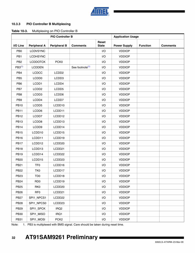
10.3.3 PIO Controller B Multiplexing
Note: 1. PB3 is multiplexed with BMS signal. Care should be taken during reset time.
Table 10-3. Multiplexing on PIO Controller B
PIO Controller B Application Usage
I/O Line Peripheral A Peripheral B CommentsReset State Power Supply Function Comments
PB0 LCDVSYNC I/O VDDIOP
PB1 LCDHSYNC I/O VDDIOP
PB2 LCDDOTCK PCK0 I/O VDDIOP
PB3(1) LCDDEN See footnote(1) I/O VDDIOP
PB4 LCDCC LCDD2 I/O VDDIOP
PB5 LCDD0 LCDD3 I/O VDDIOP
PB6 LCDD1 LCDD4 I/O VDDIOP
PB7 LCDD2 LCDD5 I/O VDDIOP
PB8 LCDD3 LCDD6 I/O VDDIOP
PB9 LCDD4 LCDD7 I/O VDDIOP
PB10 LCDD5 LCDD10 I/O VDDIOP
PB11 LCDD6 LCDD11 I/O VDDIOP
PB12 LCDD7 LCDD12 I/O VDDIOP
PB13 LCDD8 LCDD13 I/O VDDIOP
PB14 LCDD9 LCDD14 I/O VDDIOP
PB15 LCDD10 LCDD15 I/O VDDIOP
PB16 LCDD11 LCDD19 I/O VDDIOP
PB17 LCDD12 LCDD20 I/O VDDIOP
PB18 LCDD13 LCDD21 I/O VDDIOP
PB19 LCDD14 LCDD22 I/O VDDIOP
PB20 LCDD15 LCDD23 I/O VDDIOP
PB21 TF0 LCDD16 I/O VDDIOP
PB22 TK0 LCDD17 I/O VDDIOP
PB23 TD0 LCDD18 I/O VDDIOP
PB24 RD0 LCDD19 I/O VDDIOP
PB25 RK0 LCDD20 I/O VDDIOP
PB26 RF0 LCDD21 I/O VDDIOP
PB27 SPI1_NPCS1 LCDD22 I/O VDDIOP
PB28 SPI1_NPCS0 LCDD23 I/O VDDIOP
PB29 SPI1_SPCK IRQ2 I/O VDDIOP
PB30 SPI1_MISO IRQ1 I/O VDDIOP
PB31 SPI1_MOSI PCK2 I/O VDDIOP
326062LS–ATARM–23-Mar-09
AT91SAM9261 Preliminary
AT91SAM9261 Preliminary
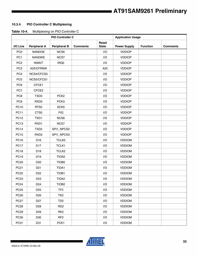
10.3.4 PIO Controller C Multiplexing
Table 10-4. Multiplexing on PIO Controller C
PIO Controller C Application Usage
I/O Line Peripheral A Peripheral B CommentsReset State Power Supply Function Comments
PC0 NANDOE NCS6 I/O VDDIOP
PC1 NANDWE NCS7 I/O VDDIOP
PC2 NWAIT IRQ0 I/O VDDIOP
PC3 A25/CFRNW A25 VDDIOP
PC4 NCS4/CFCS0 I/O VDDIOP
PC5 NCS5/CFCS1 I/O VDDIOP
PC6 CFCE1 I/O VDDIOP
PC7 CFCE2 I/O VDDIOP
PC8 TXD0 PCK2 I/O VDDIOP
PC9 RXD0 PCK3 I/O VDDIOP
PC10 RTS0 SCK0 I/O VDDIOP
PC11 CTS0 FIQ I/O VDDIOP
PC12 TXD1 NCS6 I/O VDDIOP
PC13 RXD1 NCS7 I/O VDDIOP
PC14 TXD2 SPI1_NPCS2 I/O VDDIOP
PC15 RXD2 SPI1_NPCS3 I/O VDDIOP
PC16 D16 TCLK0 I/O VDDIOM
PC17 D17 TCLK1 I/O VDDIOM
PC18 D18 TCLK2 I/O VDDIOM
PC19 D19 TIOA0 I/O VDDIOM
PC20 D20 TIOB0 I/O VDDIOM
PC21 D21 TIOA1 I/O VDDIOM
PC22 D22 TIOB1 I/O VDDIOM
PC23 D23 TIOA2 I/O VDDIOM
PC24 D24 TIOB2 I/O VDDIOM
PC25 D25 TF2 I/O VDDIOM
PC26 D26 TK2 I/O VDDIOM
PC27 D27 TD2 I/O VDDIOM
PC28 D28 RD2 I/O VDDIOM
PC29 D29 RK2 I/O VDDIOM
PC30 D30 RF2 I/O VDDIOM
PC31 D31 PCK1 I/O VDDIOM
336062LS–ATARM–23-Mar-09
10.3.5 System InterruptThe System Interrupt in Source 1 is the wired-OR of the interrupt signals coming from:
• the SDRAM Controller
• the Debug Unit
• the Periodic Interval Timer
• the Real-Time Timer
• the Watchdog Timer
• the Reset Controller
• the Power Management Controller
The clock of these peripherals cannot be deactivated and Peripheral ID 1 can only be usedwithin the Advanced Interrupt Controller.
10.3.6 External InterruptsAll external interrupt signals, i.e., the Fast Interrupt signal FIQ or the Interrupt signals IRQ0 toIRQ2, use a dedicated Peripheral ID. However, there is no clock control associated with theseperipheral IDs.
10.4 External Bus Interface• Integrates two External Memory Controllers:
– Static Memory Controller
– SDRAM Controller
• Additional logic for NAND Flash and CompactFlash support
– NAND Flash support: 8-bit as well as 16-bit devices are supported
– CompactFlash support: all modes (Attribute Memory, Common Memory, I/O, True IDE) are supported but the signals -IOIS16 (I/O and True IDE modes) and -ATA SEL (True IDE mode) are not handled.
• Optimized External Bus
– 16- or 32-bit Data Bus
– Up to 26-bit Address Bus, up to 64 Mbytes addressable
– Eight Chip Selects, each reserved to one of the eight Memory Areas
– Optimized pin multiplexing to reduce latencies on External Memories
• Configurable Chip Select Assignment Managed by EBI_CSA Register located in the MATRIX user interface
– Static Memory Controller on NCS0
– SDRAM Controller or Static Memory Controller on NCS1
– Static Memory Controller on NCS2
– Static Memory Controller on NCS3, Optional NAND Flash Support
– Static Memory Controller on NCS4 - NCS5, Optional CompactFlash Support
– Static Memory Controller on NCS6 - NCS7
346062LS–ATARM–23-Mar-09
AT91SAM9261 Preliminary
AT91SAM9261 Preliminary
10.5 Static Memory Controller• External memory mapping, 256 Mbyte address space per Chip Select Line
• Up to Eight Chip Select Lines
• 8-, 16- or 32-bit Data Bus
• Multiple Access Modes supported
– Byte Write or Byte Select Lines
– Asynchronous read in Page Mode supported (4- up to 32-byte page size)
• Multiple device adaptability
– Compliant with LCD Module
– Control signal programmable setup, pulse and hold time for each Memory Bank
• Multiple Wait State Management
– Programmable Wait State Generation
– External Wait Request
– Programmable Data Float Time
• Slow Clock Mode Supported
10.6 SDRAM Controller• Supported Devices
– Standard and Low Power SDRAM (Mobile SDRAM)
• Numerous configurations supported
– 2K, 4K, 8K Row Address Memory Parts
– SDRAM with two or four Internal Banks
– SDRAM with 16- or 32-bit Data Path
• Programming Facilities
– Word, half-word, byte access
– Automatic page break when Memory Boundary has been reached
– Multibank Ping-pong Access
– Timing parameters specified by software
– Automatic refresh operation, refresh rate is programmable
• Energy-saving Capabilities
– Self-refresh, power down and deep power down modes supported
• Error detection
– Refresh Error Interrupt
• SDRAM Power-up Initialization by software
• CAS Latency of 1, 2 and 3 supported
• Auto Precharge Command not used
356062LS–ATARM–23-Mar-09
10.7 Serial Peripheral Interface• Supports communication with serial external devices
– Four chip selects with external decoder support allow communication with up to fifteen peripherals
– Serial memories, such as DataFlash and 3-wire EEPROMs
– Serial peripherals, such as ADCs, DACs, LCD Controllers, CAN Controllers and Sensors
– External co-processors
• Master or slave serial peripheral bus interface
– 8- to 16-bit programmable data length per chip select
– Programmable phase and polarity per chip select
– Programmable transfer delays between consecutive transfers and between clock and data per chip select
– Programmable delay between consecutive transfers
– Selectable mode fault detection
• Very fast transfers supported
– Transfers with baud rates up to MCK
– The chip select line may be left active to speed up transfers on the same device
10.8 Two-wire Interface• Compatibility with standard two-wire serial memory
• One, two or three bytes for slave address
• Sequential read/write operations
10.9 USART• Programmable Baud Rate Generator
• 5- to 9-bit full-duplex synchronous or asynchronous serial communications
– 1, 1.5 or 2 stop bits in Asynchronous Mode or 1 or 2 stop bits in Synchronous Mode
– Parity generation and error detection
– Framing error detection, overrun error detection
– MSB- or LSB-first
– Optional break generation and detection
– By-8 or by-16 over-sampling receiver frequency
– Hardware handshaking RTS-CTS
– Receiver time-out and transmitter timeguard
– Optional Multi-drop Mode with address generation and detection
• RS485 with driver control signal
• ISO7816, T = 0 or T = 1 Protocols for interfacing with smart cards
– NACK handling, error counter with repetition and iteration limit
• IrDA modulation and demodulation
– Communication at up to 115.2 Kbps
366062LS–ATARM–23-Mar-09
AT91SAM9261 Preliminary
AT91SAM9261 Preliminary
• Test Modes
– Remote Loopback, Local Loopback, Automatic Echo
10.10 Synchronous Serial Controller• Provides serial synchronous communication links used in audio and telecom applications
(with CODECs in Master or Slave Modes, I2S, TDM Buses, Magnetic Card Reader and more).
• Contains an independent receiver and transmitter and a common clock divider.
• Offers a configurable frame sync and data length.
• Receiver and transmitter can be programmed to start automatically or on detection of different event on the frame sync signal.
• Receiver and transmitter include a data signal, a clock signal and a frame synchronization signal.
10.11 Timer Counter• Three 16-bit Timer Counter Channels
• Wide range of functions including:
– Frequency Measurement
– Event Counting
– Interval Measurement
– Pulse Generation
– Delay Timing
– Pulse Width Modulation
– Up/down Capabilities
• Each channel is user-configurable and contains:
– Three external clock inputs
– Five internal clock inputs
– Two multi-purpose input/output signals
• Two global registers that act on all three TC Channels
10.12 Multimedia Card Interface• Compatibility with MultiMedia Card Specification Version 2.2
• Compatibility with SD Memory Card Specification Version 1.0
• Cards clock rate up to Master Clock divided by 2
• Embedded power management to slow down clock rate when not used
• Each MCI has two slots, each supporting
– One slot for one MultiMedia Card bus (up to 30 cards) or
– One SD Memory Card
• Support for stream, block and multi-block data read and write
376062LS–ATARM–23-Mar-09
10.13 USB• USB Host Port:
– Compliance with Open HCI Rev 1.0 specification
– Compliance with USB V2.0 Full-speed and Low-speed Specification
– Supports both Low-speed 1.5 Mbps and Full-speed 12 Mbps USB devices
– Root hub integrated with two downstream USB ports
– Two embedded USB transceivers
– No overcurrent detection
– Supports power management
– Operates as a master on the Bus Matrix
• USB Device Port:
– USB V2.0 full-speed compliant, 12 Mbits per second
– Embedded USB V2.0 full-speed transceiver
– Embedded dual-port RAM for endpoints
– Suspend/Resume logic
– Ping-pong mode (two memory banks) for isochronous and bulk endpoints
– Six general-purpose endpoints:
Endpoint 0: 8 bytes, no ping-pong mode
Endpoint 1, Endpoint 2: 64 bytes, ping-pong mode
Endpoint 3: 64 bytes, no ping-pong mode
Endpoint 4, Endpoint 5: 256 bytes, ping-pong mode
• Embedded pad pull-up configurable via USB_PUCR Register located in the MATRIX user interface
10.14 LCD Controller• Single and Dual scan color and monochrome passive STN LCD panels supported
• Single scan active TFT LCD panels supported.
• 4-bit single scan, 8-bit single or dual scan, 16-bit dual scan STN interfaces supported
• Up to 24-bit single scan TFT interfaces supported
• Up to 16 gray levels for mono STN and up to 4096 colors for color STN displays
• 1, 2 bits per pixel (palletized), 4 bits per pixel (non-palletized) for mono STN
• 1, 2, 4, 8 bits per pixel (palletized), 16 bits per pixel (non-palletized) for color STN
• 1, 2, 4, 8 bits per pixel (palletized), 16, 24 bits per pixel (non-palletized) for TFT
• Single clock domain architecture
• Resolution supported up to 2048 x 2048
386062LS–ATARM–23-Mar-09
AT91SAM9261 Preliminary
AT91SAM9261 Preliminary
11. Package Drawing
Figure 11-1. 217-ball LFBGA Package Drawing
396062LS–ATARM–23-Mar-09
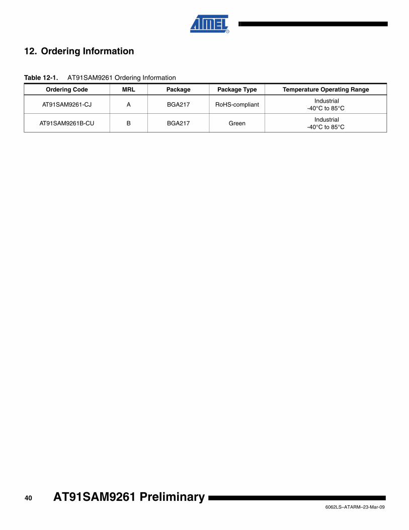
12. Ordering Information
Table 12-1. AT91SAM9261 Ordering Information
Ordering Code MRL Package Package Type Temperature Operating Range
AT91SAM9261-CJ A BGA217 RoHS-compliant Industrial
-40°C to 85°C
AT91SAM9261B-CU B BGA217 Green Industrial
-40°C to 85°C
406062LS–ATARM–23-Mar-09
AT91SAM9261 Preliminary
AT91SAM9261 Preliminary
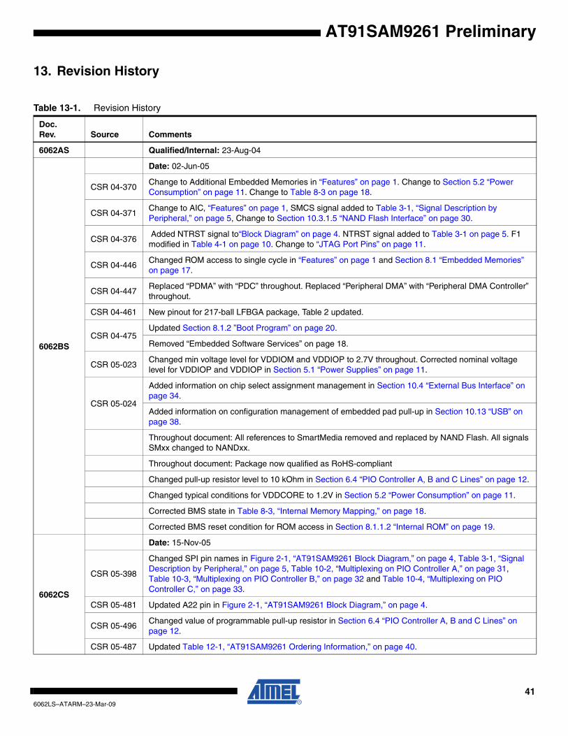
13. Revision History
Table 13-1. Revision History
Doc. Rev. Source Comments
6062AS Qualified/Internal: 23-Aug-04
6062BS
Date: 02-Jun-05
CSR 04-370Change to Additional Embedded Memories in “Features” on page 1. Change to Section 5.2 “Power Consumption” on page 11. Change to Table 8-3 on page 18.
CSR 04-371Change to AIC, “Features” on page 1, SMCS signal added to Table 3-1, “Signal Description by Peripheral,” on page 5, Change to Section 10.3.1.5 “NAND Flash Interface” on page 30.
CSR 04-376 Added NTRST signal to“Block Diagram” on page 4. NTRST signal added to Table 3-1 on page 5. F1 modified in Table 4-1 on page 10. Change to “JTAG Port Pins” on page 11.
CSR 04-446Changed ROM access to single cycle in “Features” on page 1 and Section 8.1 “Embedded Memories” on page 17.
CSR 04-447Replaced “PDMA” with “PDC” throughout. Replaced “Peripheral DMA” with “Peripheral DMA Controller” throughout.
CSR 04-461 New pinout for 217-ball LFBGA package, Table 2 updated.
CSR 04-475Updated Section 8.1.2 ”Boot Program” on page 20.
Removed “Embedded Software Services” on page 18.
CSR 05-023Changed min voltage level for VDDIOM and VDDIOP to 2.7V throughout. Corrected nominal voltage level for VDDIOP and VDDIOP in Section 5.1 “Power Supplies” on page 11.
CSR 05-024
Added information on chip select assignment management in Section 10.4 “External Bus Interface” on page 34.
Added information on configuration management of embedded pad pull-up in Section 10.13 “USB” on page 38.
Throughout document: All references to SmartMedia removed and replaced by NAND Flash. All signals SMxx changed to NANDxx.
Throughout document: Package now qualified as RoHS-compliant
Changed pull-up resistor level to 10 kOhm in Section 6.4 “PIO Controller A, B and C Lines” on page 12.
Changed typical conditions for VDDCORE to 1.2V in Section 5.2 “Power Consumption” on page 11.
Corrected BMS state in Table 8-3, “Internal Memory Mapping,” on page 18.
Corrected BMS reset condition for ROM access in Section 8.1.1.2 “Internal ROM” on page 19.
6062CS
Date: 15-Nov-05
CSR 05-398
Changed SPI pin names in Figure 2-1, “AT91SAM9261 Block Diagram,” on page 4, Table 3-1, “Signal Description by Peripheral,” on page 5, Table 10-2, “Multiplexing on PIO Controller A,” on page 31, Table 10-3, “Multiplexing on PIO Controller B,” on page 32 and Table 10-4, “Multiplexing on PIO Controller C,” on page 33.
CSR 05-481 Updated A22 pin in Figure 2-1, “AT91SAM9261 Block Diagram,” on page 4.
CSR 05-496Changed value of programmable pull-up resistor in Section 6.4 “PIO Controller A, B and C Lines” on page 12.
CSR 05-487 Updated Table 12-1, “AT91SAM9261 Ordering Information,” on page 40.
416062LS–ATARM–23-Mar-09
6062DSCorrected MIPS and speed on page 1.
2292 Added information on EBI NCS0 hwhen BMS = 0 in Table 8-3, “Internal Memory Mapping,” on page 18.
6062ES
2946Updated information on JTAGSEL in Section 3-1 “Signal Description by Peripheral” on page 5 and in Section 6.1 “JTAG Port Pins” on page 11.
2475Reformatted Section 8. “Memories” on page 16. Inserted new Figure 8-1, “AT91SAM9261 Memory Mapping,” on page 16 to show full product memory mapping.
2474Removed information on Timer Counter clock assignments in Section 10.11 “Timer Counter” on page 37.
2480 Inserted new Section 8.1.2 “Boot Strategies” on page 20 to replace Boot ROM section.
6062FS
3068Changed pin name for ball D9 to SHDN in Table 4-1, “AT91SAM9261 Pinout for 217-ball LFBGA Package (1),” on page 10.
3147 Updated information on shutdown pin in Section 6.5 “Shutdown Logic Pins” on page 12.
3067 Updated peripheral mnemonics in Figure 8-1, “AT91SAM9261 Memory Mapping,” on page 16.
3503 Added note to Table 10-1, “Peripheral Identifiers,” on page 28.
6062GS3660, 3695
Updated VDDOSC, VDDPLL and VDDIOM ranges in”Features”, Table 3-1, “Signal Description by Peripheral,” on page 5 and Section 5.2 “Power Consumption” on page 11.
3660 Added ROM to Figure 8-1, “AT91SAM9261 Memory Mapping,” on page 16.
6062HS3491
Updated Section 9.6 “Power Management Controller” on page 25 and Figure 9-3, “Power Management Controller Block Diagram,” on page 25.
Added Section 11. “Package Drawing” on page 39.
6062IS
5042
Table 10-4, “Multiplexing on PIO Controller C,” on page 33,
PCO - PC7 and PC12-PC13 power supplies are VDDIOP not VDDIOM.
Table 10-2, “Multiplexing on PIO Controller A,” on page 31PA30-PA31 power supplies are VDDIOP not VDDIOM
5027
rfo
Section 8.1.2 “Boot Strategies”, removed sentence pertaining to “remap”
Section 8.1.2.1 “BMS = 1, Boot on Embedded ROM”, added NANDFlash Boot.
4965 Section 5.1 “Power Supplies”, startup voltage slope requirements for VDDCORE and VDDBU added.
4844 Table 10-3, “Multiplexing on PIO Controller B,” on page 32, Note added to “PB3” comments
4835Figure 9-3, “Power Management Controller Block Diagram,” on page 25, in the master memory controller representation, the divider has been updated.
4241Table 4-1 on page 10, PCO - PC7, PC8 - PC11, PC12 - PC15 power supplies are VDDIOP not VDDIOM.
6062JS5250
Section 5.2 “Power Consumption”, startup voltage slope requirements for VDDCORE and VDDBU removed.
5248 In Features, on page 2: Required Power Supply updated, 3.0V to 3.6V for VDDOSC and for VDDPLL
Table 13-1. Revision History (Continued)
Doc. Rev. Source Comments
426062LS–ATARM–23-Mar-09
AT91SAM9261 Preliminary
AT91SAM9261 Preliminary
6062KS5846
5932
In Features, on page 2
Debug Unit (DBGU) updated
Section 10.9 “USART”, manchester encoding option is not avaiilable.
6062LS
5424/rfo Section 8.1.2.1 “BMS = 1, Boot on Embedded ROM”, updated.
Section 12. “Ordering Information”,updated with ordering information for chip revision B.
Table 13-1. Revision History (Continued)
Doc. Rev. Source Comments
436062LS–ATARM–23-Mar-09
Headquarters International
Atmel Corporation2325 Orchard ParkwaySan Jose, CA 95131USATel: 1(408) 441-0311Fax: 1(408) 487-2600
Atmel AsiaUnit 1-5 & 16, 19/FBEA Tower, Millennium City 5418 Kwun Tong RoadKwun Tong, KowloonHong KongTel: (852) 2245-6100Fax: (852) 2722-1369
Atmel EuropeLe Krebs8, Rue Jean-Pierre TimbaudBP 30978054 Saint-Quentin-en-Yvelines CedexFranceTel: (33) 1-30-60-70-00 Fax: (33) 1-30-60-71-11
Atmel Japan9F, Tonetsu Shinkawa Bldg.1-24-8 ShinkawaChuo-ku, Tokyo 104-0033JapanTel: (81) 3-3523-3551Fax: (81) 3-3523-7581
Product Contact
Web Sitewww.atmel.comwww.atmel.com/AT91SAM
Technical SupportAT91SAM SupportAtmel techincal support
Sales Contactswww.atmel.com/contacts/
Literature Requestswww.atmel.com/literature
Disclaimer: The information in this document is provided in connection with Atmel products. No license, express or implied, by estoppel or otherwise, to anyintellectual property right is granted by this document or in connection with the sale of Atmel products. EXCEPT AS SET FORTH IN ATMEL’S TERMS AND CONDI-TIONS OF SALE LOCATED ON ATMEL’S WEB SITE, ATMEL ASSUMES NO LIABILITY WHATSOEVER AND DISCLAIMS ANY EXPRESS, IMPLIED OR STATUTORYWARRANTY RELATING TO ITS PRODUCTS INCLUDING, BUT NOT LIMITED TO, THE IMPLIED WARRANTY OF MERCHANTABILITY, FITNESS FOR A PARTICULARPURPOSE, OR NON-INFRINGEMENT. IN NO EVENT SHALL ATMEL BE LIABLE FOR ANY DIRECT, INDIRECT, CONSEQUENTIAL, PUNITIVE, SPECIAL OR INCIDEN-TAL DAMAGES (INCLUDING, WITHOUT LIMITATION, DAMAGES FOR LOSS OF PROFITS, BUSINESS INTERRUPTION, OR LOSS OF INFORMATION) ARISING OUTOF THE USE OR INABILITY TO USE THIS DOCUMENT, EVEN IF ATMEL HAS BEEN ADVISED OF THE POSSIBILITY OF SUCH DAMAGES. Atmel makes norepresentations or warranties with respect to the accuracy or completeness of the contents of this document and reserves the right to make changes to specifica-tions and product descriptions at any time without notice. Atmel does not make any commitment to update the information contained herein. Unless specifically pro-vided otherwise, Atmel products are not suitable for, and shall not be used in, automotive applications. Atmel’s products are not intended, authorized, or warrantedfor use as components in applications intended to support or sustain life.
© 2009 Atmel Corporation. All rights reserved. Atmel®, Atmel logo and combinations thereof, DataFlash®, SAM-BA® and others are regis-tered trademarks and others are trademarks of Atmel Corporation or its subsidiaries. ARM®, the ARMPowered® logo, Thumb® and others are theregistered trademarks or trademarks of ARM Ltd. Windows® and others are the registered trademarks or trademarks of Microsoft Corporation inthe US and/or other countries. Other terms and product names may be the trademarks of others.
6062LS–ATARM–23-Mar-09


![AT91 USB HID Driver Implementation - ww1.microchip.comww1.microchip.com/downloads/en/AppNotes/doc6273.pdf · AT91 USB HID Driver Implementation 1. ... January 21, 2005. [2] Atmel](https://img.pdfslide.net/doc/110x75/5be9e0aa09d3f25b278c9e5c/at91-usb-hid-driver-implementation-ww1-at91-usb-hid-driver-implementation.jpg)