Embed Size (px)
Citation preview

AT9933Hysteretic Boost-Buck (Ćuk) LED Driver IC
Features
• Constant Current LED Driver
• Steps Input Voltage Up or Down
• Low Electromagnetic Interference (EMI)
• Variable Frequency Operation
• Internal 75V Linear Regulator
• Input and Output Current Sensing
• Input Current Limit
• Enable and Pulse-width Modulation (PWM) Dimming
• Ambient Temperature Rating of up to 125°C
Applications
• LED Lighting Applications
General Description
The AT9933 is a variable frequency PWM controller IC, designed to control an LED lamp driver using a low-noise boost-buck (Ćuk) topology. It uses patent-pending Hysteretic Current-mode control to regulate both the input and the output currents. This enables superior input surge immunity without the necessity for complex loop compensation. Input current control enables current limiting during Startup, Input Undervoltage and Output Overload conditions. The AT9933 provides a low-frequency PWM dimming input that can accept an external control signal with a duty cycle of 0%–100% and a high dimming ratio.
This AT9933-based LED driver is ideal for LED lamps. The part is rated for up to 125°C ambient temperatures.
Package Type
REF
CS2
VDD
PWMD
VIN
CS1
GND
GATE
8
7
6
5
1
2
3
4
8-lead SOIC(Top View)
See Table 2-1 for pin information.
2016 Microchip Technology Inc. DS20005597A-page 1
AT9933
Functional Block Diagram
Regulator 7.5V
VIN
CS1
CS2
PWMD
GATE
VDD
REF
GND
1.25V
AT9933
Input Comparator
Output Comparator
0mV
100mV
DS20005597A-page 2 2016 Microchip Technology Inc.
AT9933
Typical Application
VIN
GATE
CS1
GND
VDD
PWMD
CS2
REF
VDC
L1 L2
C1
Q1 D1
RCS1
RS2
RREF2 RREF1
RS1
C2
D2 (optional)
-
VO
+
C3
RCS2
D3
RD CD
AT9933
Circuit
2016 Microchip Technology Inc. DS20005597A-page 3

AT9933
1.0 ELECTRICAL CHARACTERISTICS
Absolute Maximum Ratings†
VIN to GND ................................................................................................................................................–0.5V to +75VCS1, CS2, PWMD and GATE to GND ............................................................................................. –0.3V to VDD +0.3VVDD(MAX) ................................................................................................................................................................. +12VOperating Temperature Range............................................................................................................. –40°C to +125°CJunction Temperature.......................................................................................................................................... +150°CStorage Temperature Range ............................................................................................................... –65°C to +150°CContinuous Power Dissipation (TA = +25°C):
8-lead SOIC ............................................................................................................................................ 700 mW
† Notice: Stresses above those listed under “Absolute Maximum Ratings” may cause permanent damage to the device. This is a stress rating only, and functional operation of the device at those or any other conditions above those indicated in the operational sections of this specification is not intended. Exposure to maximum rating conditions for extended periods may affect device reliability.
ELECTRICAL CHARACTERISTICS Electrical Specifications: Specifications are at TA = 25°C, VIN = Open and VDD = 7.5V unless otherwise noted.
Parameter Sym. Min. Typ. Max. Unit Conditions
INPUT
Input DC Supply Voltage Range VINDC Note 3 — 75 VDC input voltage (Note 1 and Note 2)
Shutdown Mode Supply Current IINSD — 0.5 1 mAPWMD connected to GND, VIN = 12V (Note 2)
INTERNAL REGULATOR
Internally Regulated Voltage VDD 7 7.5 9 VVIN = 8V–75V, IDD(EXT) = 0, 500 pF capacitor at GATE, PWMD = GND (Note 1)
VDD Undervoltage Lockout Threshold
UVLO 6.35 6.7 7.05 V VDD rising (Note 1)
VDD Undervoltage Lock-out Hysteresis
∆UVLO — 500 — mV
REFERENCE
REF Pin Voltage 0°C < TA < +85°C
VREF
1.212 1.25 1.288V
REF bypassed with a 0.1 µF capacitor to GND, IREF = 0, PWMD = 5VREF Pin Voltage
–40°C < TA < +125°C1.187 1.25 1.312
Line Regulation of Reference Voltage
VREFLINE 0 — 20 mVREF bypassed with a 0.1 µF capac-itor to GND, IREF = 0, VDD = 7V–9V, PWMD = 5V
Reference Output Current Range IREF –0.01 — 500 µAREF bypassed with a 0.1 µF capac-itor to GND, IREF = 0, VDD = 7V–9V, PWMD = 5V
Load Regulation of Reference Voltage
VREFLOAD 0 — 10 mVREF bypassed with a 0.1 µF capac-itor to GND, IREF = 0 µA–500 µA, PWMD = 5V
PWM DIMMING
PWMD Input Low Voltage VPWMD(LO) — — 0.8 V VDD = 7V–9V (Note 1)
PWMD Input High Voltage VPWMD(HI) 2 — — V VDD = 7V–9V (Note 1)
Note 1: Specifications apply over the full operating ambient temperature range of –40ºC < TA < +125ºC.
2: Also limited by package power dissipation limit, whichever is lower
3: Depends on the current drawn by the part. See Section 4.0 “Application Information”
DS20005597A-page 4 2016 Microchip Technology Inc.
AT9933
PWMD Pull-down Resistance RPWMD 50 100 150 kΩ VPWMD = 5V
GATE DRIVER
GATE Short Circuit Current ISOURCE 0.165 — — A VGATE = 0V
GATE Sinking Current ISINK 0.165 — — A VGATE = VDD
GATE Output Rise Time TRISE — 30 50 ns CGATE = 500 pF
GATE Output Fall Time TFALL — 30 50 ns CGATE = 500 pF
INPUT CURRENT SENSE COMPARATOR
Voltage required to turn on GATE VTURNON1 85 100 115 mVCS2 = 200 mV, CS1 increasing, GATE goes LOW to HIGH (Note 1)
Voltage required to turn off GATEVTURN-
OFF1–15 0 15 mV
CS2 = 200 mV, CS1 decreasing, GATE goes HIGH to LOW (Note 1)
Delay to Output (Turn-on) TD1,ON — 150 250 nsCS2 = 200 mV, CS1 = 50 mV to +200 mV step
Delay to Output (Turn-off) TD1,OFF — 150 250 nsCS2 = 200 mV, CS1 = 50 mV to –100 mV step
OUTPUT CURRENT SENSE COMPARATOR
Voltage required to turn on GATE VTURNON2 85 100 115 mVCS1 = 200 mV, CS2 increasing, GATE goes LOW to HIGH (Note 1)
Voltage required to turn off GATE VTURN-
OFF2–15 0 15 mV
CS1 = 200 mV, CS2 decreasing, GATE goes HIGH to LOW (Note 1)
Delay to Output (Turn-on) TD2,ON — 150 250 nsCS1 = 200 mV, CS2 = 50 mV to +200 mV step
Delay to Output (Turn-off) TD2,OFF — 150 250 nsCS1 = 200 mV, CS2 = 50 mV to –100 mV step
TEMPERATURE SPECIFICATIONS
Parameter Sym. Min. Typ. Max. Unit Conditions
TEMPERATURE RANGE
Operating Temperature TA –40 — +125 °C
Junction Temperature TJ — — +150 °C
Storage Temperature TS –65 — +150 °C
PACKAGE THERMAL RESISTANCE
8-lead SOIC JA — +101 — °C/W Note 1
Note 1: Mounted on a FR-4 board, 25 mm x 25 mm x 1.57 mm
ELECTRICAL CHARACTERISTICS (CONTINUED)Electrical Specifications: Specifications are at TA = 25°C, VIN = Open and VDD = 7.5V unless otherwise noted.
Parameter Sym. Min. Typ. Max. Unit Conditions
Note 1: Specifications apply over the full operating ambient temperature range of –40ºC < TA < +125ºC.
2: Also limited by package power dissipation limit, whichever is lower
3: Depends on the current drawn by the part. See Section 4.0 “Application Information”
2016 Microchip Technology Inc. DS20005597A-page 5
AT9933
2.0 PIN DESCRIPTION
The details on the pins of AT9933 are listed on Table 2-1. Refer to Package Type for the location of the pins.
TABLE 2-1: PIN FUNCTION TABLE
Pin Number Pin Name Description
1 VIN This pin is the input of an 8V–75V voltage regulator.
2 CS1This pin is used to sense the input and output currents of the boost-buck converter. It is a non-inverting input of the internal comparator.
3 GNDThis is the ground return for all the internal circuitry. This pin must be electrically connected to the ground of the power train.
4 GATEThis pin is the output gate driver for an external N-channel power Metal-oxide Semiconductor Field-effect Transistor (MOSFET).
5 PWMDWhen this pin is left open or pulled to GND, the gate driver is disabled. Pulling the pin to a voltage greater than 2V will enable the gate driver output.
6 VDDThis is a power supply pin for all internal circuits. It must be bypassed to GND with a low-ESR capacitor greater than 0.1 µF.
7 CS2This pin is used to sense the input and output currents of the boost-buck converter. It is a non-inverting input of the internal comparator.
8 REFThis pin provides accurate reference voltage. It must be bypassed with a 0.01 µF–0.1 µF capacitor to GND.
DS20005597A-page 6 2016 Microchip Technology Inc.
AT9933
3.0 DETAILED DESCRIPTION
3.1 Power Topology
The AT9933 is optimized to drive a Continuous Conduction Mode (CCM) boost-buck DC/DC converter topology commonly referred to as Ćuk converter. (Refer to Typical Application Circuit.) This power converter topology offers numerous advantages useful for driving high-brightness light-emitting diodes (HB LED). These advantages include step-up or step-down voltage conversion ratio and low input and output current ripple. The output load is decoupled from the input voltage with a capacitor, making the driver inherently failure-safe for the output load.
The AT9933 offers a simple and effective control technique for a boost-buck LED driver. It uses two Hysteretic mode controllers—one for the input and one for the output. The outputs of these two hysteretic comparators are ANDED and used to drive the external FET. This control scheme gives accurate current control and constant output current in the presence of input voltage transients without the need for complicated loop design.
3.2 Input Voltage Regulator
The AT9933 can be powered directly from its VIN pin that can withstand a maximum voltage of up to 75V. When a voltage is applied to the VIN pin, the AT9933 seeks to regulate a constant 7.5V (typical) at the VDDpin. The regulator also has a built-in undervoltage lockout which shuts off the IC when the voltage at the VDD pin falls below the UVLO threshold.
The VDD pin must be bypassed by a low-ESR capacitor (≥0.1 μF) to provide a low-impedance path for the high frequency current of the output gate driver.
The input current drawn from the VIN pin is the sum of the 1 mA current drawn by the internal circuit and the current drawn by the gate driver, which in turn depends on the switching frequency and the gate charge of the external FET. Refer to Equation 3-1.
EQUATION 3-1:
IIN 1mA QG fS+=
In the above equation, fS is the switching frequency, and QG is the gate charge of the external FET which can be obtained from the data sheet of the FET.
3.3 Minimum Input Voltage at VIN Pin
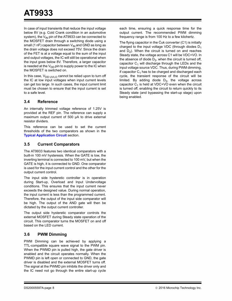
The minimum input voltage at which the converter will start and stop depends on the minimum voltage drop required for the linear regulator. The internal linear regulator will control the voltage at the VDD pin when VIN is between 8V and 75V. However, when the VIN is less than 8V, the converter will still function as long as
the VDD is greater than the undervoltage lockout. Thus, under certain conditions, the converter will be able to start at VIN voltages of less than 8V. The start/stop voltages at the VIN pin can be determined using the maximum voltage drop across the linear regulator as a function of the current drawn. The data for ambient temperatures 25ºC and 125ºC are shown in Figure 3-1 below:
3.5
3.0
2.5
2.0
1.5
1.0
0.5
00 1 2 3 4 5 6 7
IIN (mA)
Volta
ge D
rop
(V)
125OC
25OC
FIGURE 3-1: Maximum Voltage Drop vs. Input Current.
Assume an ambient temperature of 125°C. Provided that the IC is driving a 15 nC gate charge FET at 300 kHz, the total input current is estimated to be 5.5 mA (using Equation 3-1). At this input current, the maximum voltage drop from Figure 3-1 can be approximately estimated to be VDROP = 2.7V. However, before the IC starts switching, the current drawn will be 1 mA. At this current level, the voltage drop is approximately VDROP1 = 0.5V. Thus, the start/stop VINvoltages can be computed as shown in Equation 3-2 and Equation 3-3:
EQUATION 3-2:
VIN START– UVLOMAX VDROP1+=
6.95V 0.5V+=
7.45V=
EQUATION 3-3:
VIN STOP– UVLOMAX UVLO VDROP+–=
6.95V 0.5V– 2.7V+=
9.15V=
Note: Since the gate driver draws too much cur-rent in this situation, VIN-START is less than VIN-STOP. The control IC will oscillate between on and off if the input voltage is between the start and stop voltages. In these circumstances, it is recommended that the input voltage be kept higher than VIN-STOP. The IC will operate normally if the input voltage is kept higher than 9.2V.
2016 Microchip Technology Inc. DS20005597A-page 7
AT9933
In case of input transients that reduce the input voltage below 8V (e.g. Cold Crank condition in an automotive system), the VIN pin of the AT9933 can be connected to the MOSFET drain through a switching diode using a small (1 nF) capacitor between VIN and GND as long as the drain voltage does not exceed 75V. Since the drain of the FET is at a voltage equal to the sum of the input and output voltages, the IC will still be operational when the input goes below 8V. Therefore, a larger capacitor is needed at the VDD pin to supply power to the IC when the MOSFET is switched on.
In this case, VDD UVLO cannot be relied upon to turn off the IC at low input voltages when input current levels can get too large. In such cases, the input current limit must be chosen to ensure that the input current is set to a safe level.
3.4 Reference
An internally trimmed voltage reference of 1.25V is provided at the REF pin. The reference can supply a maximum output current of 500 µA to drive external resistor dividers.
This reference can be used to set the current thresholds of the two comparators as shown in the Typical Application Circuit section.
3.5 Current Comparators
The AT9933 features two identical comparators with a built-in 100 mV hysteresis. When the GATE is low, the inverting terminal is connected to 100 mV, but when the GATE is high, it is connected to GND. One comparator is used for the input current control and the other for the output current control.
The input side hysteretic controller is in operation during Start-up, Overload and Input Undervoltage conditions. This ensures that the input current never exceeds the designed value. During normal operation, the input current is less than the programmed current. Therefore, the output of the input side comparator will be high. The output of the AND gate will then be dictated by the output current controller.
The output side hysteretic comparator controls the external MOSFET during Steady state operation of the circuit. This comparator turns the MOSFET on and off based on the LED current.
3.6 PWM Dimming
PWM Dimming can be achieved by applying a TTL-compatible square wave signal to the PWM pin. When the PWMD pin is pulled high, the gate driver is enabled and the circuit operates normally. When the PWMD pin is left open or connected to GND, the gate driver is disabled and the external MOSFET turns off. The signal at the PWMD pin inhibits the driver only and the IC need not go through the entire start-up cycle
each time, ensuring a quick response time for the output current. The recommended PWM dimming frequency range is from 100 Hz to a few kilohertz.
The flying capacitor in the Ćuk converter (C1) is initially charged to the input voltage VDC (through diodes D1and D2). When the circuit is turned on and reaches Steady state, the voltage across C1 will be VDC+VO. In the absence of diode D2, when the circuit is turned off, capacitor C1 will discharge through the LEDs and the input voltage source VDC. Thus, during PWM dimming, if capacitor C1 has to be charged and discharged each cycle, the transient response of the circuit will be limited. By adding diode D2, the voltage across capacitor C1 is held at VDC+VO even when the circuit is turned off, enabling the circuit to return quickly to its Steady state (and bypassing the start-up stage) upon being enabled.
DS20005597A-page 8 2016 Microchip Technology Inc.
AT9933
4.0 APPLICATION INFORMATION
4.1 Overvoltage Protection
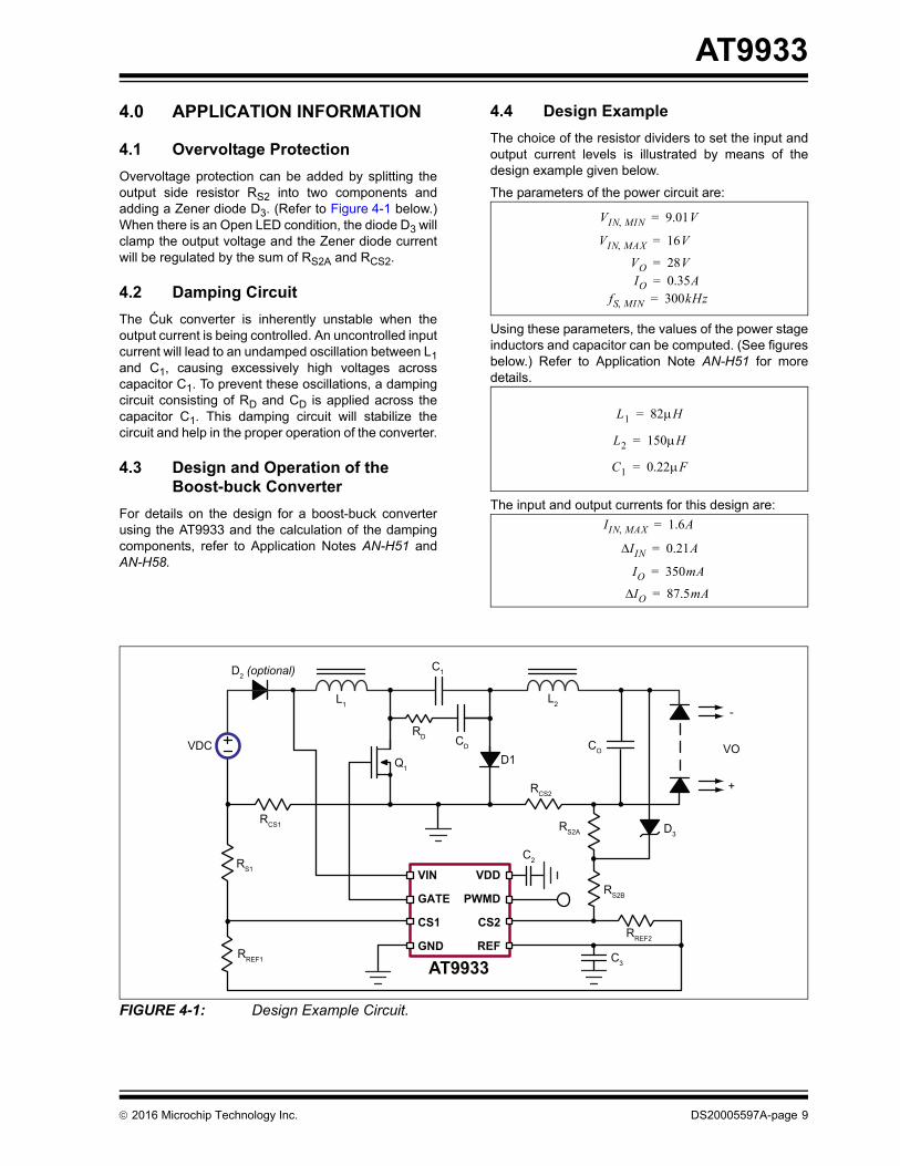
Overvoltage protection can be added by splitting the output side resistor RS2 into two components and adding a Zener diode D3. (Refer to Figure 4-1 below.) When there is an Open LED condition, the diode D3 will clamp the output voltage and the Zener diode current will be regulated by the sum of RS2A and RCS2.
4.2 Damping Circuit
The Ćuk converter is inherently unstable when the output current is being controlled. An uncontrolled input current will lead to an undamped oscillation between L1and C1, causing excessively high voltages across capacitor C1. To prevent these oscillations, a damping circuit consisting of RD and CD is applied across the capacitor C1. This damping circuit will stabilize the circuit and help in the proper operation of the converter.
4.3 Design and Operation of the Boost-buck Converter
For details on the design for a boost-buck converter using the AT9933 and the calculation of the damping components, refer to Application Notes AN-H51 and AN-H58.
4.4 Design Example
The choice of the resistor dividers to set the input and output current levels is illustrated by means of the design example given below.
The parameters of the power circuit are:
VIN MIN 9.01V=
VIN MAX 16V=
VO 28V=IO 0.35A=
fS MIN 300kHz=
Using these parameters, the values of the power stage inductors and capacitor can be computed. (See figures below.) Refer to Application Note AN-H51 for more details.
L1 82H=
L2 150H=
C1 0.22F=
The input and output currents for this design are:
IIN MAX 1.6A=
I IN 0.21A=
IO 350mA=
IO 87.5mA=
VIN
GATE
CS1
GND
VDD
PWMD
CS2
REF
VDC
L1 L2
C1
Q1 D1
RCS1 RS2A
RREF2
RREF1
RS1
C2
D2 (optional)
-
VO
+
C3
RCS2
CO
RD CD
AT9933
RS2B
D3
FIGURE 4-1: Design Example Circuit.
2016 Microchip Technology Inc. DS20005597A-page 9
AT9933
4.5 Current Limits
The current sense resistor RCS2, combined with the other resistors RS2 and RREF2, determines the output current limits.
The resistors can be chosen using Equation 4-1 and Equation 4-2.
EQUATION 4-1:
I RCS 1.2VRS
RREF------------- 0.05V–=
Where I is the current (either IO or IIN) and ∆I is the peak-to-peak ripple in the current (either ∆IO or ∆IIN).
EQUATION 4-2:
I RCS 0.1VRS
RREF------------- 0.1V+=
Where I is the current (either IO or IIN) and ∆I is the peak-to-peak ripple in the current (either ∆IO or ∆IIN).
For the input side, the current level used in the equations should be larger than the maximum input current, so that it does not interfere with the normal operation of the circuit. The peak input current can be computed as shown in Equation 4-3.
EQUATION 4-3:
IIN PK IIN MAXIIN2---------- +=
1.706A=
Assuming a 30% peak-to-peak ripple when the converter is in Input Current Limit mode, the minimum value of the input current is calculated as seen in Equation 4-4.
EQUATION 4-4:
ILIM MIN 0.85 IIN LIM=
Setting
ILIM MIN 1.05 IIN PK=
The current level to limit the converter can then be computed. See equation Equation 4-5.
EQUATION 4-5:
IIN LIM1.050.85---------- IIN PK=
2.1A=
Using IO = 350 mA and ∆IO = 87.5 mA in Equation 4-1 and Equation 4-2, RCS2 = 1.78Ω and RS2/RREF2 = 0.5625.
Before the design of the output side is complete, overvoltage protection has to be included in the design. For this application, choose a 33V Zener diode. This is the voltage at which the output will clamp in case of an Open LED condition. For a 350 mW diode, the maximum current rating at 33V works out to about 10 mA. Using a 2.5 mA current level during Open LED conditions, and assuming the same RS2/RREF2 ratio, the Zener current limiting resistor can be determined as illustrated in Equation 4-6.
EQUATION 4-6:
RCS RS2A+ 120=
Choose the following values for the resistors:
RCS2 = 1.65Ω, 1/4W, 1%
RREF2 = 10 kΩ, 1/8W, 1%
RS2A = 100Ω, 1/8W, 1%
RS2B = 5.23 kΩ, 1/8W, 1%
The current sense resistor needs to be at least a 1/4W, 1% resistor.
Similarly, using IIN = 2.1A and ∆IIN = 0.3 x IIN = 0.63 in Equation 4-1 and Equation 4-2, the following values can be determined:
RS1
RREF1--------------- 0.442=
PRCS1 I2
IN LIM RCS1=
Choose the following values for the resistors:
RCS1 = parallel combination of three 0.68Ω, 1/2W, 5% resistors
RREF1 = 10kΩ, 1/8W, 1%
RS1 = 4.42kΩ, 1/8W, 1%
RCS1 0.228=
1W=
DS20005597A-page 10 2016 Microchip Technology Inc.

AT9933
5.0 PACKAGING INFORMATION
5.1 Package Marking Information
Legend: XX...X Product Code or Customer-specific informationY Year code (last digit of calendar year)YY Year code (last 2 digits of calendar year)WW Week code (week of January 1 is week ‘01’)NNN Alphanumeric traceability code Pb-free JEDEC® designator for Matte Tin (Sn)* This package is Pb-free. The Pb-free JEDEC designator ( )
can be found on the outer packaging for this package.
Note: In the event the full Microchip part number cannot be marked on one line, it will be carried over to the next line, thus limiting the number of available characters for product code or customer-specific information. Package may or not include the corporate logo.
3e
3e
8-lead SOIC Example
NNN
XXXXXXXXYYWWe3
222
AT9933LG1645e3
2016 Microchip Technology Inc. DS20005597A-page 11

AT9933
Note: For the most current package drawings, see the Microchip Packaging Specification at www.microchip.com/packaging.
DS20005597A-page 12 2016 Microchip Technology Inc.
2016 Microchip Technology Inc. DS20005597A-page 13
AT9933
APPENDIX A: REVISION HISTORY
Revision A (October 2016)
• Converted Supertex Doc# DSFP-AT9933 to Microchip DS20005597A
• Changed the quantity of the 8-lead SOIC package from 3000/Reel to 3300/Reel
• Made minor text changes throughout the docu-ment
AT9933
DS20005597A-page 14 2016 Microchip Technology Inc.
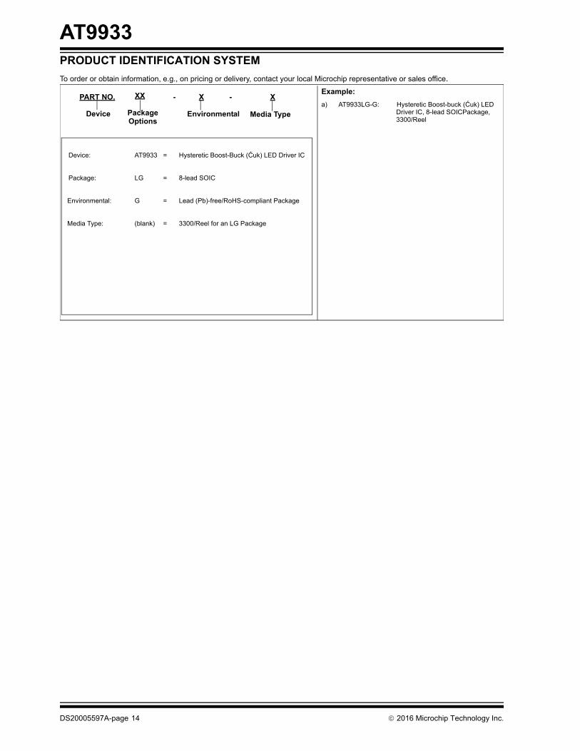
PRODUCT IDENTIFICATION SYSTEM
To order or obtain information, e.g., on pricing or delivery, contact your local Microchip representative or sales office.
Example:
a) AT9933LG-G: Hysteretic Boost-buck (Ćuk) LED Driver IC, 8-lead SOICPackage, 3300/Reel
PART NO.
Device
Device: AT9933 = Hysteretic Boost-Buck (Ćuk) LED Driver IC
Package: LG = 8-lead SOIC
Environmental: G = Lead (Pb)-free/RoHS-compliant Package
Media Type: (blank) = 3300/Reel for an LG Package
XX
Package
- X - X
Environmental Media Type Options
Note the following details of the code protection feature on Microchip devices:
• Microchip products meet the specification contained in their particular Microchip Data Sheet.
• Microchip believes that its family of products is one of the most secure families of its kind on the market today, when used in the intended manner and under normal conditions.
• There are dishonest and possibly illegal methods used to breach the code protection feature. All of these methods, to our knowledge, require using the Microchip products in a manner outside the operating specifications contained in Microchip’s Data Sheets. Most likely, the person doing so is engaged in theft of intellectual property.
• Microchip is willing to work with the customer who is concerned about the integrity of their code.
• Neither Microchip nor any other semiconductor manufacturer can guarantee the security of their code. Code protection does not mean that we are guaranteeing the product as “unbreakable.”
Code protection is constantly evolving. We at Microchip are committed to continuously improving the code protection features of our products. Attempts to break Microchip’s code protection feature may be a violation of the Digital Millennium Copyright Act. If such acts allow unauthorized access to your software or other copyrighted work, you may have a right to sue for relief under that Act.
Information contained in this publication regarding device applications and the like is provided only for your convenience and may be superseded by updates. It is your responsibility to ensure that your application meets with your specifications. MICROCHIP MAKES NO REPRESENTATIONS OR WARRANTIES OF ANY KIND WHETHER EXPRESS OR IMPLIED, WRITTEN OR ORAL, STATUTORY OR OTHERWISE, RELATED TO THE INFORMATION, INCLUDING BUT NOT LIMITED TO ITS CONDITION, QUALITY, PERFORMANCE, MERCHANTABILITY OR FITNESS FOR PURPOSE. Microchip disclaims all liability arising from this information and its use. Use of Microchip devices in life support and/or safety applications is entirely at the buyer’s risk, and the buyer agrees to defend, indemnify and hold harmless Microchip from any and all damages, claims, suits, or expenses resulting from such use. No licenses are conveyed, implicitly or otherwise, under any Microchip intellectual property rights unless otherwise stated.
2016 Microchip Technology Inc.
Microchip received ISO/TS-16949:2009 certification for its worldwide headquarters, design and wafer fabrication facilities in Chandler and Tempe, Arizona; Gresham, Oregon and design centers in California and India. The Company’s quality system processes and procedures are for its PIC® MCUs and dsPIC® DSCs, KEELOQ® code hopping devices, Serial EEPROMs, microperipherals, nonvolatile memory and analog products. In addition, Microchip’s quality system for the design and manufacture of development systems is ISO 9001:2000 certified.
QUALITYMANAGEMENTSYSTEMCERTIFIEDBYDNV
== ISO/TS16949==
Trademarks
The Microchip name and logo, the Microchip logo, AnyRate, dsPIC, FlashFlex, flexPWR, Heldo, JukeBlox, KeeLoq, KeeLoq logo, Kleer, LANCheck, LINK MD, MediaLB, MOST, MOST logo, MPLAB, OptoLyzer, PIC, PICSTART, PIC32 logo, RightTouch, SpyNIC, SST, SST Logo, SuperFlash and UNI/O are registered trademarks of Microchip Technology Incorporated in the U.S.A. and other countries.
ClockWorks, The Embedded Control Solutions Company, ETHERSYNCH, Hyper Speed Control, HyperLight Load, IntelliMOS, mTouch, Precision Edge, and QUIET-WIRE are registered trademarks of Microchip Technology Incorporated in the U.S.A.
Analog-for-the-Digital Age, Any Capacitor, AnyIn, AnyOut, BodyCom, chipKIT, chipKIT logo, CodeGuard, dsPICDEM, dsPICDEM.net, Dynamic Average Matching, DAM, ECAN, EtherGREEN, In-Circuit Serial Programming, ICSP, Inter-Chip Connectivity, JitterBlocker, KleerNet, KleerNet logo, MiWi, motorBench, MPASM, MPF, MPLAB Certified logo, MPLIB, MPLINK, MultiTRAK, NetDetach, Omniscient Code Generation, PICDEM, PICDEM.net, PICkit, PICtail, PureSilicon, RightTouch logo, REAL ICE, Ripple Blocker, Serial Quad I/O, SQI, SuperSwitcher, SuperSwitcher II, Total Endurance, TSHARC, USBCheck, VariSense, ViewSpan, WiperLock, Wireless DNA, and ZENA are trademarks of Microchip Technology Incorporated in the U.S.A. and other countries.
SQTP is a service mark of Microchip Technology Incorporated in the U.S.A.
Silicon Storage Technology is a registered trademark of Microchip Technology Inc. in other countries.
GestIC is a registered trademarks of Microchip Technology Germany II GmbH & Co. KG, a subsidiary of Microchip Technology Inc., in other countries.
All other trademarks mentioned herein are property of their respective companies.
© 2016, Microchip Technology Incorporated, Printed in the U.S.A., All Rights Reserved.
ISBN: 978-1-5224-0995-3
DS20005597A-page 15
DS20005597A-page 16 2016 Microchip Technology Inc.
AMERICASCorporate Office2355 West Chandler Blvd.Chandler, AZ 85224-6199Tel: 480-792-7200 Fax: 480-792-7277Technical Support: http://www.microchip.com/supportWeb Address: www.microchip.com
AtlantaDuluth, GA Tel: 678-957-9614 Fax: 678-957-1455
Austin, TXTel: 512-257-3370
BostonWestborough, MA Tel: 774-760-0087 Fax: 774-760-0088
ChicagoItasca, IL Tel: 630-285-0071 Fax: 630-285-0075
ClevelandIndependence, OH Tel: 216-447-0464 Fax: 216-447-0643
DallasAddison, TX Tel: 972-818-7423 Fax: 972-818-2924
DetroitNovi, MI Tel: 248-848-4000
Houston, TX Tel: 281-894-5983
IndianapolisNoblesville, IN Tel: 317-773-8323Fax: 317-773-5453
Los AngelesMission Viejo, CA Tel: 949-462-9523 Fax: 949-462-9608
New York, NY Tel: 631-435-6000
San Jose, CA Tel: 408-735-9110
Canada - TorontoTel: 905-695-1980 Fax: 905-695-2078
ASIA/PACIFICAsia Pacific OfficeSuites 3707-14, 37th FloorTower 6, The GatewayHarbour City, Kowloon
Hong KongTel: 852-2943-5100Fax: 852-2401-3431
Australia - SydneyTel: 61-2-9868-6733Fax: 61-2-9868-6755
China - BeijingTel: 86-10-8569-7000 Fax: 86-10-8528-2104
China - ChengduTel: 86-28-8665-5511Fax: 86-28-8665-7889
China - ChongqingTel: 86-23-8980-9588Fax: 86-23-8980-9500
China - DongguanTel: 86-769-8702-9880
China - GuangzhouTel: 86-20-8755-8029
China - HangzhouTel: 86-571-8792-8115 Fax: 86-571-8792-8116
China - Hong Kong SARTel: 852-2943-5100 Fax: 852-2401-3431
China - NanjingTel: 86-25-8473-2460Fax: 86-25-8473-2470
China - QingdaoTel: 86-532-8502-7355Fax: 86-532-8502-7205
China - ShanghaiTel: 86-21-5407-5533 Fax: 86-21-5407-5066
China - ShenyangTel: 86-24-2334-2829Fax: 86-24-2334-2393
China - ShenzhenTel: 86-755-8864-2200 Fax: 86-755-8203-1760
China - WuhanTel: 86-27-5980-5300Fax: 86-27-5980-5118
China - XianTel: 86-29-8833-7252Fax: 86-29-8833-7256
ASIA/PACIFICChina - XiamenTel: 86-592-2388138 Fax: 86-592-2388130
China - ZhuhaiTel: 86-756-3210040 Fax: 86-756-3210049
India - BangaloreTel: 91-80-3090-4444 Fax: 91-80-3090-4123
India - New DelhiTel: 91-11-4160-8631Fax: 91-11-4160-8632
India - PuneTel: 91-20-3019-1500
Japan - OsakaTel: 81-6-6152-7160 Fax: 81-6-6152-9310
Japan - TokyoTel: 81-3-6880- 3770 Fax: 81-3-6880-3771
Korea - DaeguTel: 82-53-744-4301Fax: 82-53-744-4302
Korea - SeoulTel: 82-2-554-7200Fax: 82-2-558-5932 or 82-2-558-5934
Malaysia - Kuala LumpurTel: 60-3-6201-9857Fax: 60-3-6201-9859
Malaysia - PenangTel: 60-4-227-8870Fax: 60-4-227-4068
Philippines - ManilaTel: 63-2-634-9065Fax: 63-2-634-9069
SingaporeTel: 65-6334-8870Fax: 65-6334-8850
Taiwan - Hsin ChuTel: 886-3-5778-366Fax: 886-3-5770-955
Taiwan - KaohsiungTel: 886-7-213-7828
Taiwan - TaipeiTel: 886-2-2508-8600 Fax: 886-2-2508-0102
Thailand - BangkokTel: 66-2-694-1351Fax: 66-2-694-1350
EUROPEAustria - WelsTel: 43-7242-2244-39Fax: 43-7242-2244-393
Denmark - CopenhagenTel: 45-4450-2828 Fax: 45-4485-2829
France - ParisTel: 33-1-69-53-63-20 Fax: 33-1-69-30-90-79
Germany - DusseldorfTel: 49-2129-3766400
Germany - KarlsruheTel: 49-721-625370
Germany - MunichTel: 49-89-627-144-0 Fax: 49-89-627-144-44
Italy - Milan Tel: 39-0331-742611 Fax: 39-0331-466781
Italy - VeniceTel: 39-049-7625286
Netherlands - DrunenTel: 31-416-690399 Fax: 31-416-690340
Poland - WarsawTel: 48-22-3325737
Spain - MadridTel: 34-91-708-08-90Fax: 34-91-708-08-91
Sweden - StockholmTel: 46-8-5090-4654
UK - WokinghamTel: 44-118-921-5800Fax: 44-118-921-5820
Worldwide Sales and Service
06/23/16