Embed Size (px)
Citation preview
APPLICATION NOTE
Atmel AT03462: ATSAM3X and ATSAM3A Series - Checklist
Atmel ARM Cortex-M3 Product Family (SAM3)
Introduction
A good hardware design comes from a perfect schematic. Therefore this Application Note is a schematic review check list for systems embedding the Atmel® SAM3X/A series of ARM® Cortex®-M3, Thumb-2-based microcontrollers.
It gives requirements concerning the different pin connections that must be considered before starting any new board design and describes the minimum hardware resources required to quickly develop an application with the SAM3X/A devices. It does not consider PCB layout constraints.
It also gives advice regarding low-power design constraints to minimize power consumption.
This Application Note is not intended to be exhaustive. Its objective is to cover as many configurations of use as possible.
The Check List table has a column reserved for reviewing designers to verify that the line item has been checked.
Features
• Associated documentation
• Schematic checklists (Powering, Clocks, Reset, PIO…)
• SAM3X/A boot program constraints
• Suggested reading
• Revision history
42187A−SAM−10/2013
Atmel AT03462: ATSAM3X and ATSAM3A Series - Checklist [APPLICATION NOTE] 42187A−SAM−10/2013
2
Table of Contents
1. Associated Documentation ................................................................. 3
2. Schematic Checklist ........................................................................... 4 2.1 Powering ........................................................................................................... 4
2.1.1 Single Power Supply ........................................................................... 4 2.1.2 Core Externally Supplied .................................................................... 6 2.1.3 Backup Supply .................................................................................... 8
2.2 Clock, Oscillator, and PLL ............................................................................... 10 2.3 ICE and JTAG ................................................................................................. 11 2.4 RESET/TEST .................................................................................................. 12 2.5 Shutdown/Wakeup Logic ................................................................................ 12 2.6 PIO …. ............................................................................................................ 13 2.7 ADC …. .......................................................................................................... 13 2.8 DAC …. .......................................................................................................... 13 2.9 USB OTG HS .................................................................................................. 14
2.9.1 USB OTGHS Typical Connection Examples ..................................... 15 2.9.1.1 Device Mode: Bus-Powered Device ................................ 15 2.9.1.2 Self-Powered Device ...................................................... 15 2.9.1.3 Host and OTG Modes ..................................................... 16
2.10 Ethernet .......................................................................................................... 16 2.11 CAN …. .......................................................................................................... 16 2.12 Static Memory Controller ................................................................................. 17
3. External Bus Interface (EBI) Hardware Interface .............................. 18
4. SAM3X/A Boot Program Constraints ................................................ 20 4.1 SAM-BA Boot .................................................................................................. 20
5. Suggested Reading .......................................................................... 21 5.1 Device Datasheet ............................................................................................ 21 5.2 Evaluation Kit User Guide ............................................................................... 21 5.3 USB Specification ........................................................................................... 21 5.4 USB High Speed Design Guidelines ............................................................... 21 5.5 ARM Documentation on Cortex-M3 Core ........................................................ 21
6. Revision History ............................................................................... 22
Atmel AT03462: ATSAM3X and ATSAM3A Series - Checklist [APPLICATION NOTE] 42187A−SAM−10/2013
3
1. Associated Documentation Before going further into this application note, it is strongly recommended to check the latest documents for the SAM3X/A Microcontrollers family on the Atmel website.
Table 1-1 gives the associated documentation needed to support full understanding of this application note.
Table 1-1. Associated Documentation
Information Document Title
User Manual Electrical/Mechanical Characteristics Ordering information Errata
ATSAM3X/ATSAM3A Product Datasheet
Internal architecture of processor Thumb-2 instruction set Embedded in-circuit-emulator
This part is integrated and formatted according to the core integration in the SAM3S series. This information is fully detailed in the ATSAM3X/A Product Datasheet. Cortex-M3 Technical Reference Manual (available from ARM Ltd.)
Evaluation Kit User Guide ATSAM3X-EK Evaluation Board User Guide
Atmel AT03462: ATSAM3X and ATSAM3A Series - Checklist [APPLICATION NOTE] 42187A−SAM−10/2013
4
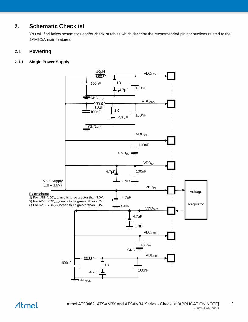
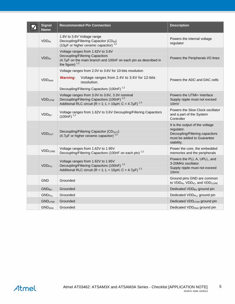
2. Schematic Checklist You will find below schematics and/or checklist tables which describe the recommended pin connections related to the SAM3X/A main features.
2.1 Powering
2.1.1 Single Power Supply
VDDUTMI 10µH
Restrictions: 1) For USB, VDDUTMI needs to be greater than 3.0V. 2) For ADC, VDDANA needs to be greater than 2.0V. 3) For DAC, VDDANA needs to be greater than 2.4V.
VDDIO
GND
100nF 4.7µF
VDDANA GNDUTMI
100nF
100nF 4.7µF
1R 100nF
4.7µF
10µH 100nF 1R
GNDANA
100nF
VDDBU
VDDPLL
GNDPLL
100nF 4.7µF
1R 100nF
GNDBU
VDDOUT
100nF GND
VDDIN
VDDCORE
Main Supply (1.8 – 3.6V)
GND
4.7µF
Voltage
Regulator
GND
4.7µF
Atmel AT03462: ATSAM3X and ATSAM3A Series - Checklist [APPLICATION NOTE] 42187A−SAM−10/2013
5
Signal Name
Recommended Pin Connection Description
VDDIN
1.8V to 3.6V Voltage range Decoupling/Filtering Capacitor (CDIN) (10µF or higher ceramic capacitor) 1,2
Powers the internal voltage regulator
VDDIO
Voltage ranges from 1.62V to 3.6V Decoupling/Filtering Capacitors (4.7µF on the main branch and 100nF on each pin as described in the figure) 1,2
Powers the Peripherals I/O lines
VDDANA
Voltage ranges from 2.0V to 3.6V for 10-bits resolution
Warning: Voltage ranges from 2.4V to 3.6V for 12-bits resolution.
Decoupling/Filtering Capacitors (100nF) 1,2
Powers the ADC and DAC cells
VDDUTMI
Voltage ranges from 3.0V to 3.6V, 3.3V nominal Decoupling/Filtering Capacitors (100nF) 1,2 Additional RLC circuit (R = 1; L = 10µH; C = 4.7µF) 1,3
Powers the UTMI+ interface Supply ripple must not exceed 10mV
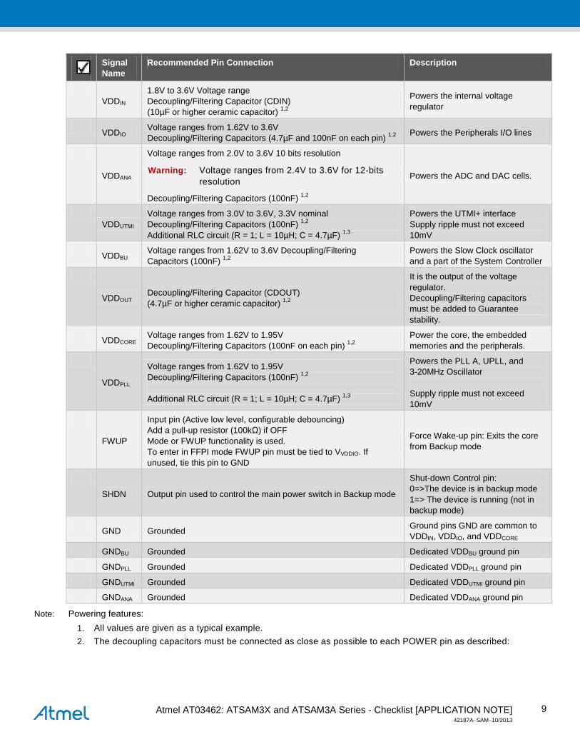
VDDBU Voltage ranges from 1.62V to 3.6V Decoupling/Filtering Capacitors
(100nF) 1,2
Powers the Slow Clock oscillator and a part of the System Controller
VDDOUT Decoupling/Filtering Capacitor (CDOUT) (4.7µF or higher ceramic capacitor) 1,2
It is the output of the voltage regulator. Decoupling/Filtering capacitors must be added to Guarantee stability.
VDDCORE Voltage ranges from 1.62V to 1.95V Decoupling/Filtering Capacitors (100nF on each pin) 1,2
Power the core, the embedded memories and the peripherals
VDDPLL Voltage ranges from 1.62V to 1.95V Decoupling/Filtering Capacitors (100nF) 1,2 Additional RLC circuit (R = 1; L = 10µH; C = 4.7µF) 1,3
Powers the PLL A, UPLL, and 3-20MHz oscillator. Supply ripple must not exceed 10mV.
GND Grounded Ground pins GND are common to VDDIN, VDDIO, and VDDCORE
GNDBU Grounded Dedicated VDDBU ground pin
GNDPLL Grounded Dedicated VDDPLL ground pin
GNDUTMI Grounded Dedicated VDDUTMI ground pin
GNDANA Grounded Dedicated VDDANA ground pin
Atmel AT03462: ATSAM3X and ATSAM3A Series - Checklist [APPLICATION NOTE] 42187A−SAM−10/2013
6
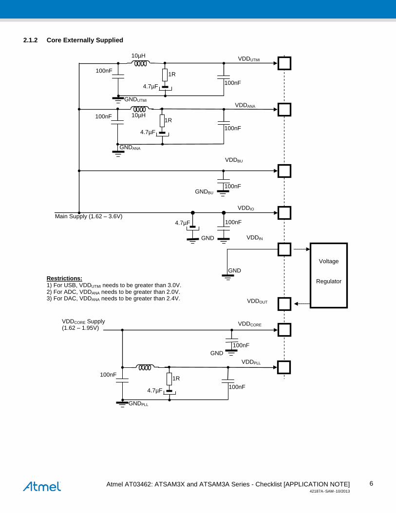
2.1.2 Core Externally Supplied
Main Supply (1.62 – 3.6V) VDDIO
GND
Restrictions: 1) For USB, VDDUTMI needs to be greater than 3.0V. 2) For ADC, VDDANA needs to be greater than 2.0V. 3) For DAC, VDDANA needs to be greater than 2.4V.
100nF 4.7µF
Voltage
Regulator
VDDUTMI
VDDANA GNDUTMI
100nF
100nF 4.7µF
10µH
1R 100nF
4.7µF
10µH 100nF 1R
GNDANA
100nF
VDDBU
VDDPLL
GNDPLL
100nF 4.7µF
1R 100nF
VDDCORE Supply (1.62 – 1.95V)
GND
GNDBU
VDDOUT
100nF GND
VDDIN
VDDCORE
Atmel AT03462: ATSAM3X and ATSAM3A Series - Checklist [APPLICATION NOTE] 42187A−SAM−10/2013
7
Signal Name
Recommended Pin Connection Description
VDDIN Grounded Powers the internal voltage regulator not use in this case
VDDIO Voltage ranges from 1.62V to 3.6V Decoupling/Filtering Capacitors (4.7µF and 100nF on each) 1,2 Powers the Peripherals I/O lines
VDDANA
Voltage ranges from 2.0V to 3.6V for 10 bits resolution.
Warning: Voltage ranges from 2.4V to 3.6V for 12-bits resolution.
Decoupling/Filtering Capacitors (100nF) 1,2
Powers the ADC and DAC cells
VDDUTMI
Voltage ranges from 3.0V to 3.6V, 3.3V nominal Decoupling/Filtering Capacitors (100nF) 1,2 Additional RLC circuit (R = 1; L = 10µH; C = 4.7µF) 1,3
Powers the UTMI+ interface Supply ripple must not exceed 10mV
VDDBU Voltage ranges from 1.62V to 3.6V Decoupling/Filtering Capacitors
(100nF) 1,2
Powers the Slow Clock oscillator and a part of the System Controller
VDDOUT Not Connected or Decoupling/Filtering capacitors can be added to guarantee stability.
It is the output of the voltage regulator
VDDCORE Voltage ranges from 1.62V to 1.95V Decoupling/Filtering Capacitors (100nF on each pin) 1,2
Power the core, the embedded memories and the peripherals
VDDPLL
Voltage ranges from 1.62V to 1.95V Decoupling/Filtering Capacitors (100nF) 1,2 Additional RLC circuit (R = 1; L = 10µH; C = 4.7µF) 1,3
Powers the PLL A, UPLL and 3-20MHz Oscillator. Supply ripple must not exceed 10mV.
GND Grounded Ground pins GND are common to VDDIN, VDDIO, and VDDCORE
GNDBU Grounded Dedicated VDDBU ground pin
GNDPLL Grounded Dedicated VDDPLL ground pin
GNDUTMI Grounded Dedicated VDDUTMI ground pin
GNDANA Grounded Dedicated VDDANA ground pin
Atmel AT03462: ATSAM3X and ATSAM3A Series - Checklist [APPLICATION NOTE] 42187A−SAM−10/2013
8
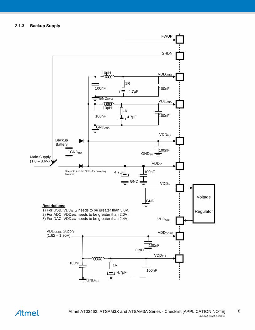
2.1.3 Backup Supply
FWUP
Main Supply (1.8 – 3.6V)
4.7µF
VDDIO
GND
Restrictions: 1) For USB, VDDUTMI needs to be greater than 3.0V. 2) For ADC, VDDANA needs to be greater than 2.0V. 3) For DAC, VDDANA needs to be greater than 2.4V.
100nF 4.7µF
Voltage
Regulator
VDDUTMI
VDDANA GNDUTMI
100nF
100nF
10µH
1R 100nF
4.7µF
10µH
100nF 1R
GNDANA
100nF
VDDBU
VDDPLL
GNDPLL
100nF 4.7µF
1R 100nF
VDDCORE Supply (1.62 – 1.95V)
GND
GNDBU
VDDOUT
100nF GND
VDDIN
VDDCORE
GNDBU
Backup Battery +
See note 4 in the Notes for powering features
SHDN
Atmel AT03462: ATSAM3X and ATSAM3A Series - Checklist [APPLICATION NOTE] 42187A−SAM−10/2013
9
Signal Name
Recommended Pin Connection Description
VDDIN
1.8V to 3.6V Voltage range Decoupling/Filtering Capacitor (CDIN) (10µF or higher ceramic capacitor) 1,2
Powers the internal voltage regulator
VDDIO Voltage ranges from 1.62V to 3.6V Decoupling/Filtering Capacitors (4.7µF and 100nF on each pin) 1,2 Powers the Peripherals I/O lines
VDDANA
Voltage ranges from 2.0V to 3.6V 10 bits resolution
Warning: Voltage ranges from 2.4V to 3.6V for 12-bits resolution
Decoupling/Filtering Capacitors (100nF) 1,2
Powers the ADC and DAC cells.
VDDUTMI
Voltage ranges from 3.0V to 3.6V, 3.3V nominal Decoupling/Filtering Capacitors (100nF) 1,2 Additional RLC circuit (R = 1; L = 10µH; C = 4.7µF) 1,3
Powers the UTMI+ interface Supply ripple must not exceed 10mV
VDDBU Voltage ranges from 1.62V to 3.6V Decoupling/Filtering Capacitors (100nF) 1,2
Powers the Slow Clock oscillator and a part of the System Controller
VDDOUT Decoupling/Filtering Capacitor (CDOUT) (4.7µF or higher ceramic capacitor) 1,2
It is the output of the voltage regulator. Decoupling/Filtering capacitors must be added to Guarantee stability.
VDDCORE Voltage ranges from 1.62V to 1.95V Decoupling/Filtering Capacitors (100nF on each pin) 1,2
Power the core, the embedded memories and the peripherals.
VDDPLL
Voltage ranges from 1.62V to 1.95V Decoupling/Filtering Capacitors (100nF) 1,2 Additional RLC circuit (R = 1; L = 10µH; C = 4.7µF) 1,3
Powers the PLL A, UPLL, and 3-20MHz Oscillator Supply ripple must not exceed 10mV
FWUP
Input pin (Active low level, configurable debouncing) Add a pull-up resistor (100kΩ) if OFF Mode or FWUP functionality is used. To enter in FFPI mode FWUP pin must be tied to VVDDIO. If unused, tie this pin to GND
Force Wake-up pin: Exits the core from Backup mode
SHDN Output pin used to control the main power switch in Backup mode
Shut-down Control pin: 0=>The device is in backup mode 1=> The device is running (not in backup mode)
GND Grounded Ground pins GND are common to VDDIN, VDDIO, and VDDCORE
GNDBU Grounded Dedicated VDDBU ground pin
GNDPLL Grounded Dedicated VDDPLL ground pin
GNDUTMI Grounded Dedicated VDDUTMI ground pin
GNDANA Grounded Dedicated VDDANA ground pin
Note: Powering features: 1. All values are given as a typical example. 2. The decoupling capacitors must be connected as close as possible to each POWER pin as described:
Atmel AT03462: ATSAM3X and ATSAM3A Series - Checklist [APPLICATION NOTE] 42187A−SAM−10/2013
10
3. The filtering RLC circuit is given as an example. Depending on the application the user may only need a 100nF
decoupling capacitor. 4. The two diodes provide a “switch over circuit” (for illustration purpose) between the backup battery and the
main supply, when the system is put in backup mode.
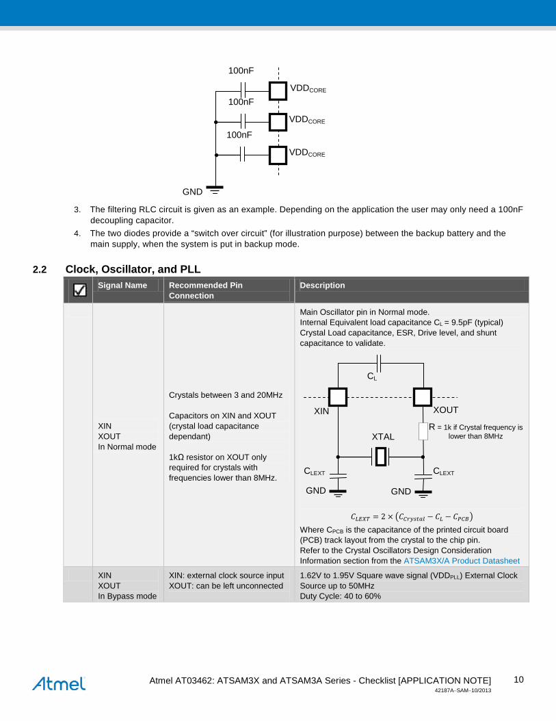
2.2 Clock, Oscillator, and PLL
Signal Name Recommended Pin Connection
Description
XIN XOUT In Normal mode
Crystals between 3 and 20MHz Capacitors on XIN and XOUT (crystal load capacitance dependant) 1kΩ resistor on XOUT only required for crystals with frequencies lower than 8MHz.
Main Oscillator pin in Normal mode. Internal Equivalent load capacitance CL = 9.5pF (typical) Crystal Load capacitance, ESR, Drive level, and shunt capacitance to validate.
𝐶𝐿𝐸𝑋𝑇 = 2 × 𝐶𝐶𝑟𝑦𝑠𝑡𝑎𝑙 − 𝐶𝐿 − 𝐶𝑃𝐶𝐵
Where CPCB is the capacitance of the printed circuit board (PCB) track layout from the crystal to the chip pin. Refer to the Crystal Oscillators Design Consideration Information section from the ATSAM3X/A Product Datasheet
XIN XOUT In Bypass mode
XIN: external clock source input XOUT: can be left unconnected
1.62V to 1.95V Square wave signal (VDDPLL) External Clock Source up to 50MHz Duty Cycle: 40 to 60%
GND GND
XIN XOUT
XTAL
CLEXT CLEXT
CL
R = 1k if Crystal frequency is lower than 8MHz
GND
VDDCORE
VDDCORE
VDDCORE
100nF
100nF
100nF
Atmel AT03462: ATSAM3X and ATSAM3A Series - Checklist [APPLICATION NOTE] 42187A−SAM−10/2013
11
Signal Name Recommended Pin Connection
Description
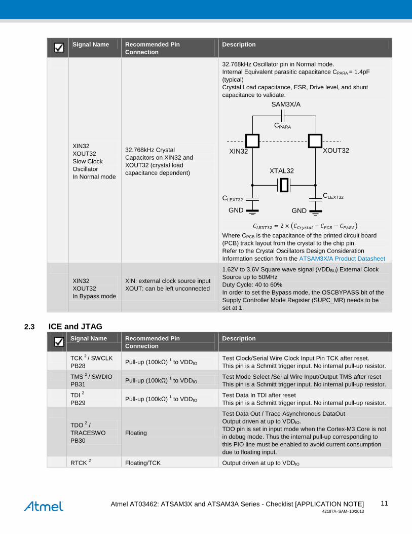
XIN32 XOUT32 Slow Clock Oscillator In Normal mode
32.768kHz Crystal Capacitors on XIN32 and XOUT32 (crystal load capacitance dependent)
32.768kHz Oscillator pin in Normal mode. Internal Equivalent parasitic capacitance CPARA = 1.4pF (typical) Crystal Load capacitance, ESR, Drive level, and shunt capacitance to validate.
𝐶𝐿𝐸𝑋𝑇32 = 2 × 𝐶𝐶𝑟𝑦𝑠𝑡𝑎𝑙 − 𝐶𝑃𝐶𝐵 − 𝐶𝑃𝐴𝑅𝐴
Where CPCB is the capacitance of the printed circuit board (PCB) track layout from the crystal to the chip pin. Refer to the Crystal Oscillators Design Consideration Information section from the ATSAM3X/A Product Datasheet
XIN32 XOUT32 In Bypass mode
XIN: external clock source input XOUT: can be left unconnected
1.62V to 3.6V Square wave signal (VDDBU) External Clock Source up to 50MHz Duty Cycle: 40 to 60% In order to set the Bypass mode, the OSCBYPASS bit of the Supply Controller Mode Register (SUPC_MR) needs to be set at 1.
2.3 ICE and JTAG
Signal Name Recommended Pin Connection
Description
TCK 2 / SWCLK PB28 Pull-up (100kΩ) 1 to VDDIO Test Clock/Serial Wire Clock Input Pin TCK after reset.
This pin is a Schmitt trigger input. No internal pull-up resistor.
TMS 2 / SWDIO PB31 Pull-up (100kΩ) 1 to VDDIO Test Mode Select /Serial Wire Input/Output TMS after reset
This pin is a Schmitt trigger input. No internal pull-up resistor.
TDI 2 PB29 Pull-up (100kΩ) 1 to VDDIO Test Data In TDI after reset
This pin is a Schmitt trigger input. No internal pull-up resistor.
TDO 2 / TRACESWO PB30
Floating
Test Data Out / Trace Asynchronous DataOut Output driven at up to VDDIO. TDO pin is set in input mode when the Cortex-M3 Core is not in debug mode. Thus the internal pull-up corresponding to this PIO line must be enabled to avoid current consumption due to floating input.
RTCK 2 Floating/TCK Output driven at up to VDDIO
GND GND
XIN32 XOUT32
XTAL32
CLEXT32 CLEXT32
SAM3X/A
CPARA
Atmel AT03462: ATSAM3X and ATSAM3A Series - Checklist [APPLICATION NOTE] 42187A−SAM−10/2013
12
JTAGSEL 2,3
In harsh environments, it is strongly recommended to tie this pin to GNDBU if not used or to add an external low value resistor (such as 1kΩ 1).
Internal pull-down resistor to GNDBU (15kΩ). Must be tied to VDDBU to enter JTAG Boundary Scan.
Notes: 1. All values are given as a typical example. 2. It is recommended to establish accessibility to a JTAG connector for debug in any case. 3. In a well-shielded environment subject to low magnetic and electric field interference, the pin may be left
unconnected. In noisy environments, a connection to ground is recommended. 4. All JTAG pins can be used as GPIO if they are not used for JTAG functions.
2.4 RESET/TEST
Signal Name Recommended Pin Connection
Description
NRST Application dependent. Can be connected to a push button for hardware reset
Microcontroller Reset Input/Output pin NRST is controlled by the Reset Controller (RSTC). An internal pull-up resistor to VDDIO (100kΩ) is available for User Reset and External Reset control.
NRSTB 1
In harsh environments, it is recommended to add an external capacitor (10nF) between NRSTB and VDDBU
Asynchronous Microcontroller Reset Input pin The NRSTB pin integrates a permanent pull-up resistor of about 15kΩ. This allows connection of a simple push button on the NRSTB pin as a system-user reset. In all modes, this pin will reset the chip including the Backup region (RTC, RTT, and Supply Controller). It reacts as the Power-on reset. It can be used as an external system reset source.
TST 1
In harsh environments, It is strongly Recommended to tie this pin to GNDBU if not used or to add an external low-value resistor (such as 1kΩ).
Test Mode Select Input pin Internal pull-down resistor to GNDBU (15kΩ).
Note: 1. In a well-shielded environment subject to low magnetic and electric field interference, the pin may be left unconnected. In noisy environments, a connection to ground is recommended.
2.5 Shutdown/Wakeup Logic
Signal Name Recommended Pin Connection
Description
FWUP
Input pin (low level, configurable deboucing) If used Need external Pull-up 0V to VDDBU
Force Wake up pin: Exits the core from Backup mode FWUP to be set at VDDBU in JTAG Boundary Scan. FWUP behavior can be configured through the Supply Controller (SUPC).
SHDN
Output pin used to control the main power switch in Back-up mode for example
Shut-down Control pin: 0=>The device is in backup mode 1=> The device is running (not in backup mode)
Atmel AT03462: ATSAM3X and ATSAM3A Series - Checklist [APPLICATION NOTE] 42187A−SAM−10/2013
13
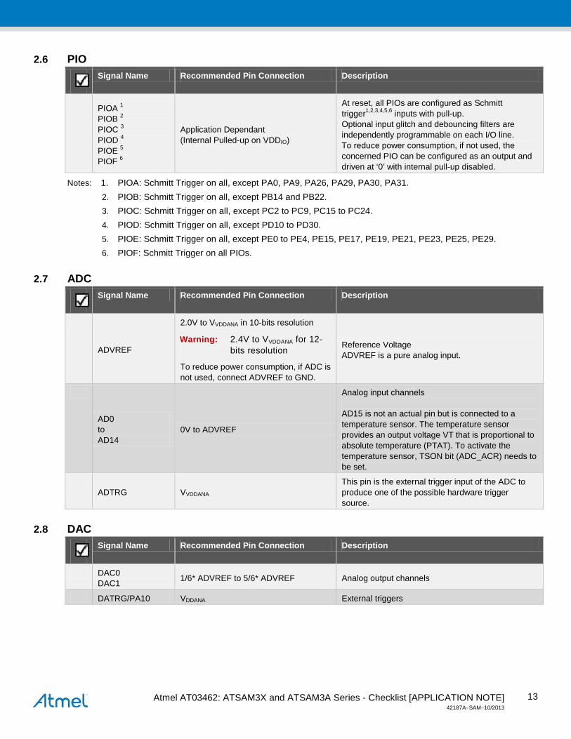
2.6 PIO
Signal Name Recommended Pin Connection Description
PIOA 1 PIOB 2 PIOC 3 PIOD 4 PIOE 5 PIOF 6
Application Dependant (Internal Pulled-up on VDDIO)
At reset, all PIOs are configured as Schmitt trigger1,2,3,4,5,6 inputs with pull-up. Optional input glitch and debouncing filters are independently programmable on each I/O line. To reduce power consumption, if not used, the concerned PIO can be configured as an output and driven at ‘0’ with internal pull-up disabled.
Notes: 1. PIOA: Schmitt Trigger on all, except PA0, PA9, PA26, PA29, PA30, PA31. 2. PIOB: Schmitt Trigger on all, except PB14 and PB22. 3. PIOC: Schmitt Trigger on all, except PC2 to PC9, PC15 to PC24. 4. PIOD: Schmitt Trigger on all, except PD10 to PD30. 5. PIOE: Schmitt Trigger on all, except PE0 to PE4, PE15, PE17, PE19, PE21, PE23, PE25, PE29. 6. PIOF: Schmitt Trigger on all PIOs.
2.7 ADC
Signal Name Recommended Pin Connection Description
ADVREF
2.0V to VVDDANA in 10-bits resolution
Warning: 2.4V to VVDDANA for 12-bits resolution
To reduce power consumption, if ADC is not used, connect ADVREF to GND.
Reference Voltage ADVREF is a pure analog input.
AD0 to AD14
0V to ADVREF
Analog input channels AD15 is not an actual pin but is connected to a temperature sensor. The temperature sensor provides an output voltage VT that is proportional to absolute temperature (PTAT). To activate the temperature sensor, TSON bit (ADC_ACR) needs to be set.
ADTRG VVDDANA
This pin is the external trigger input of the ADC to produce one of the possible hardware trigger source.
2.8 DAC
Signal Name Recommended Pin Connection Description
DAC0 DAC1 1/6* ADVREF to 5/6* ADVREF Analog output channels
DATRG/PA10 VDDANA External triggers
Atmel AT03462: ATSAM3X and ATSAM3A Series - Checklist [APPLICATION NOTE] 42187A−SAM−10/2013
14
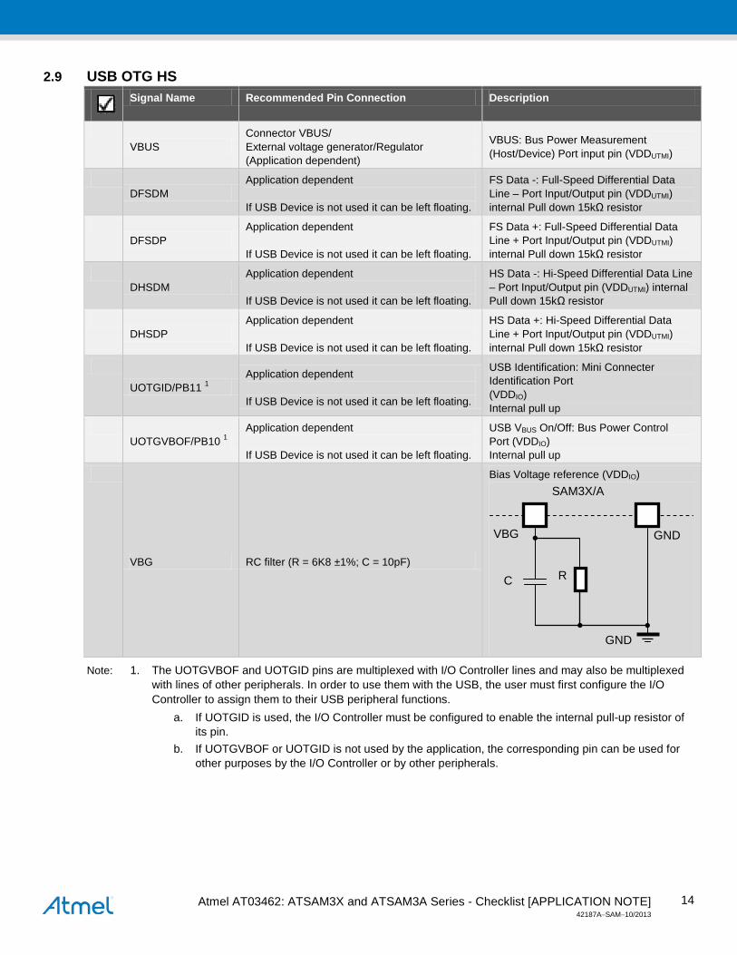
2.9 USB OTG HS
Signal Name Recommended Pin Connection Description
VBUS
Connector VBUS/ External voltage generator/Regulator (Application dependent)
VBUS: Bus Power Measurement (Host/Device) Port input pin (VDDUTMI)
DFSDM
Application dependent If USB Device is not used it can be left floating.
FS Data -: Full-Speed Differential Data Line – Port Input/Output pin (VDDUTMI) internal Pull down 15kΩ resistor
DFSDP
Application dependent If USB Device is not used it can be left floating.
FS Data +: Full-Speed Differential Data Line + Port Input/Output pin (VDDUTMI) internal Pull down 15kΩ resistor
DHSDM
Application dependent If USB Device is not used it can be left floating.
HS Data -: Hi-Speed Differential Data Line – Port Input/Output pin (VDDUTMI) internal Pull down 15kΩ resistor
DHSDP
Application dependent If USB Device is not used it can be left floating.
HS Data +: Hi-Speed Differential Data Line + Port Input/Output pin (VDDUTMI) internal Pull down 15kΩ resistor
UOTGID/PB11 1 Application dependent If USB Device is not used it can be left floating.
USB Identification: Mini Connecter Identification Port (VDDIO) Internal pull up
UOTGVBOF/PB10 1
Application dependent If USB Device is not used it can be left floating.
USB VBUS On/Off: Bus Power Control Port (VDDIO) Internal pull up
VBG RC filter (R = 6K8 ±1%; C = 10pF)
Bias Voltage reference (VDDIO)
Note: 1. The UOTGVBOF and UOTGID pins are multiplexed with I/O Controller lines and may also be multiplexed with lines of other peripherals. In order to use them with the USB, the user must first configure the I/O Controller to assign them to their USB peripheral functions.
a. If UOTGID is used, the I/O Controller must be configured to enable the internal pull-up resistor of its pin.
b. If UOTGVBOF or UOTGID is not used by the application, the corresponding pin can be used for other purposes by the I/O Controller or by other peripherals.
GND
VBG
C
SAM3X/A
GND
R
Atmel AT03462: ATSAM3X and ATSAM3A Series - Checklist [APPLICATION NOTE] 42187A−SAM−10/2013
15
2.9.1 USB OTGHS Typical Connection Examples
2.9.1.1 Device Mode: Bus-Powered Device
2.9.1.2 Self-Powered Device
VBUS
VBUS UOTGID
UOTGVBOF
DFSDM
DFSDP
DHSDM
DHSDP
ID
D-
D+
GND
US
B C
onne
ctor
R=39
R=39
VBUS
VBUS UOTGID
UOTGVBOF
DFSDM
DFSDP
DHSDM
DHSDP
ID
D-
D+
GND
3.3V Regulator
US
B C
onne
ctor
VDD
R=39
R=39
Atmel AT03462: ATSAM3X and ATSAM3A Series - Checklist [APPLICATION NOTE] 42187A−SAM−10/2013
16
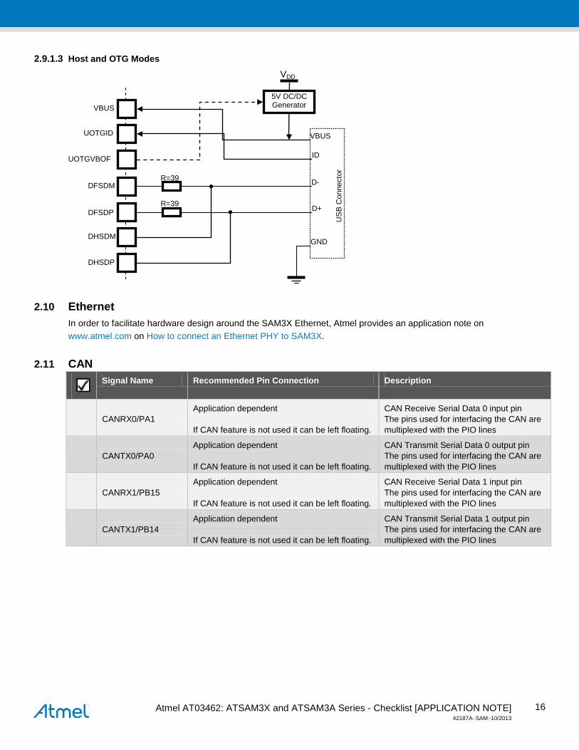
2.9.1.3 Host and OTG Modes
2.10 Ethernet In order to facilitate hardware design around the SAM3X Ethernet, Atmel provides an application note on www.atmel.com on How to connect an Ethernet PHY to SAM3X.
2.11 CAN
Signal Name Recommended Pin Connection Description
CANRX0/PA1
Application dependent If CAN feature is not used it can be left floating.
CAN Receive Serial Data 0 input pin The pins used for interfacing the CAN are multiplexed with the PIO lines
CANTX0/PA0
Application dependent If CAN feature is not used it can be left floating.
CAN Transmit Serial Data 0 output pin The pins used for interfacing the CAN are multiplexed with the PIO lines
CANRX1/PB15
Application dependent If CAN feature is not used it can be left floating.
CAN Receive Serial Data 1 input pin The pins used for interfacing the CAN are multiplexed with the PIO lines
CANTX1/PB14
Application dependent If CAN feature is not used it can be left floating.
CAN Transmit Serial Data 1 output pin The pins used for interfacing the CAN are multiplexed with the PIO lines
VBUS
VBUS UOTGID
UOTGVBOF
DFSDM
DFSDP
DHSDM
DHSDP
ID
D-
D+
GND
5V DC/DC Generator
US
B C
onne
ctor
VDD
R=39
R=39
Atmel AT03462: ATSAM3X and ATSAM3A Series - Checklist [APPLICATION NOTE] 42187A−SAM−10/2013
17
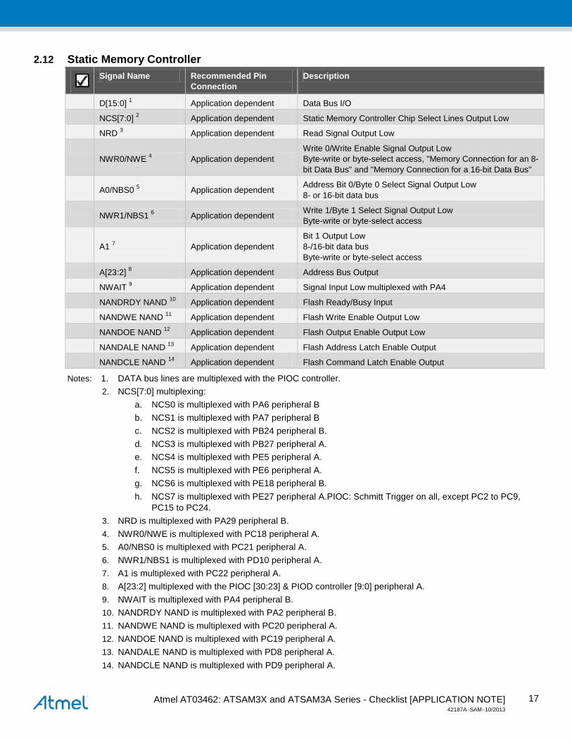
2.12 Static Memory Controller
Signal Name Recommended Pin Connection
Description
D[15:0] 1 Application dependent Data Bus I/O
NCS[7:0] 2 Application dependent Static Memory Controller Chip Select Lines Output Low
NRD 3 Application dependent Read Signal Output Low
NWR0/NWE 4 Application dependent
Write 0/Write Enable Signal Output Low Byte-write or byte-select access, "Memory Connection for an 8-bit Data Bus" and "Memory Connection for a 16-bit Data Bus"
A0/NBS0 5 Application dependent Address Bit 0/Byte 0 Select Signal Output Low 8- or 16-bit data bus
NWR1/NBS1 6 Application dependent Write 1/Byte 1 Select Signal Output Low Byte-write or byte-select access
A1 7 Application dependent
Bit 1 Output Low 8-/16-bit data bus Byte-write or byte-select access
A[23:2] 8 Application dependent Address Bus Output
NWAIT 9 Application dependent Signal Input Low multiplexed with PA4
NANDRDY NAND 10 Application dependent Flash Ready/Busy Input
NANDWE NAND 11 Application dependent Flash Write Enable Output Low
NANDOE NAND 12 Application dependent Flash Output Enable Output Low
NANDALE NAND 13 Application dependent Flash Address Latch Enable Output
NANDCLE NAND 14 Application dependent Flash Command Latch Enable Output
Notes: 1. DATA bus lines are multiplexed with the PIOC controller. 2. NCS[7:0] multiplexing:
a. NCS0 is multiplexed with PA6 peripheral B b. NCS1 is multiplexed with PA7 peripheral B c. NCS2 is multiplexed with PB24 peripheral B. d. NCS3 is multiplexed with PB27 peripheral A. e. NCS4 is multiplexed with PE5 peripheral A. f. NCS5 is multiplexed with PE6 peripheral A. g. NCS6 is multiplexed with PE18 peripheral B. h. NCS7 is multiplexed with PE27 peripheral A.PIOC: Schmitt Trigger on all, except PC2 to PC9,
PC15 to PC24. 3. NRD is multiplexed with PA29 peripheral B. 4. NWR0/NWE is multiplexed with PC18 peripheral A. 5. A0/NBS0 is multiplexed with PC21 peripheral A. 6. NWR1/NBS1 is multiplexed with PD10 peripheral A. 7. A1 is multiplexed with PC22 peripheral A. 8. A[23:2] multiplexed with the PIOC [30:23] & PIOD controller [9:0] peripheral A. 9. NWAIT is multiplexed with PA4 peripheral B. 10. NANDRDY NAND is multiplexed with PA2 peripheral B. 11. NANDWE NAND is multiplexed with PC20 peripheral A. 12. NANDOE NAND is multiplexed with PC19 peripheral A. 13. NANDALE NAND is multiplexed with PD8 peripheral A. 14. NANDCLE NAND is multiplexed with PD9 peripheral A.
Atmel AT03462: ATSAM3X and ATSAM3A Series - Checklist [APPLICATION NOTE] 42187A−SAM−10/2013
18
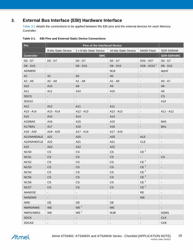
3. External Bus Interface (EBI) Hardware Interface Table 3-1 details the connections to be applied between the EBI pins and the external devices for each Memory Controller:
Table 3-1. EBI Pins and External Static Device Connections
Pin Pins of the Interfaced Device
8-bits Static Device 2 x 8-bits Static Device 16-bits Static Device NAND Flash SDR-SDRAM
Controller SMC SDR-SDRAMC
D0 - D7 D0 - D7 D0 - D7 D0 - D7 I/O0 - I/O7 D0 - D7
D8 - D15 - D8 - D15 D8 - D15 I/O8 - I/O15 1 D8 - D15
A0/NBS0 - NLB - dqm0
A1 A1 A0 A0 - -
A2 - A9 A2 - A9 A1 - A8 A1 - A8 - A0 - A7
A10 A10 A9 A9 - A8
A11 A11 A10 A10 - A9
SDCS - - - - CS
SDA10 - - - - A10
A12 A12 A11 A11 - -
A13 - A14 A13 - A14 A12 - A13 A12 - A13 - A11 - A12
A15 A15 A14 A14 - -
A16/BA0 A16 A15 A15 - BA0
A17/BA1 A17 A16 A16 - BA1
A18 - A20 A18 - A20 A17 - A19 A17 - A19 - -
A21/NANDALE A21 A20 A20 ALE -
A22/NANDCLE A22 A21 A21 CLE -
A23 A23 A22 A22 - -
NCS0 CS CS CS CE 3 -
NCS1 CS CS CS - CS
NCS2 CS CS CS CE 3 -
NCS3 CS CS CS CE 3 -
NCS4 CS CS CS CE 3 -
NCS5 CS CS CS CE 3 -
NCS6 CS CS CS CE 3 -
NCS7 CS CS CS CE 3 -
NANDOE - - - RE -
NANDWE - - - WE -
NRD OE OE OE -
NWR0/NWE WE WE 2 WE -
NWR1/NBS1 WE WE 2 NUB - DQM1
SDCK - - - - CLK
SDCKE - - - - CKE
Atmel AT03462: ATSAM3X and ATSAM3A Series - Checklist [APPLICATION NOTE] 42187A−SAM−10/2013
19
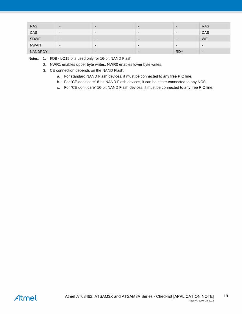
RAS - - - - RAS
CAS - - - - CAS
SDWE - - - - WE
NWAIT - - - - -
NANDRDY - - - RDY -
Notes: 1. I/O8 - I/O15 bits used only for 16-bit NAND Flash. 2. NWR1 enables upper byte writes. NWR0 enables lower byte writes. 3. CE connection depends on the NAND Flash.
a. For standard NAND Flash devices, it must be connected to any free PIO line. b. For “CE don’t care” 8-bit NAND Flash devices, it can be either connected to any NCS. c. For “CE don’t care” 16-bit NAND Flash devices, it must be connected to any free PIO line.
Atmel AT03462: ATSAM3X and ATSAM3A Series - Checklist [APPLICATION NOTE] 42187A−SAM−10/2013
20
4. SAM3X/A Boot Program Constraints See AT91SAM Boot Program section of the SAM3X/A Series Datasheet for more details on the boot program.
4.1 SAM-BA Boot The SAM-BA® Boot Assistant supports serial communication via the UART or USB device port:
• UART0 hardware requirements: • 12.000MHz quartz or 12.000MHz external clock on XIN, or • no quartz or external clock on XIN, or • below 5.0MHz quartz or below 5.0MHz external clock on XIN.
• • USB device hardware requirements: • 12.000MHz quartz or 12.000MHz external clock on XIN. • 12MHz must be ±500ppm and 1.8V Square Wave Signal.
“SAM-BA Boot uses the first 2048 bytes of the SRAM for variables and stacks. The remaining available size can be used for user's code.”
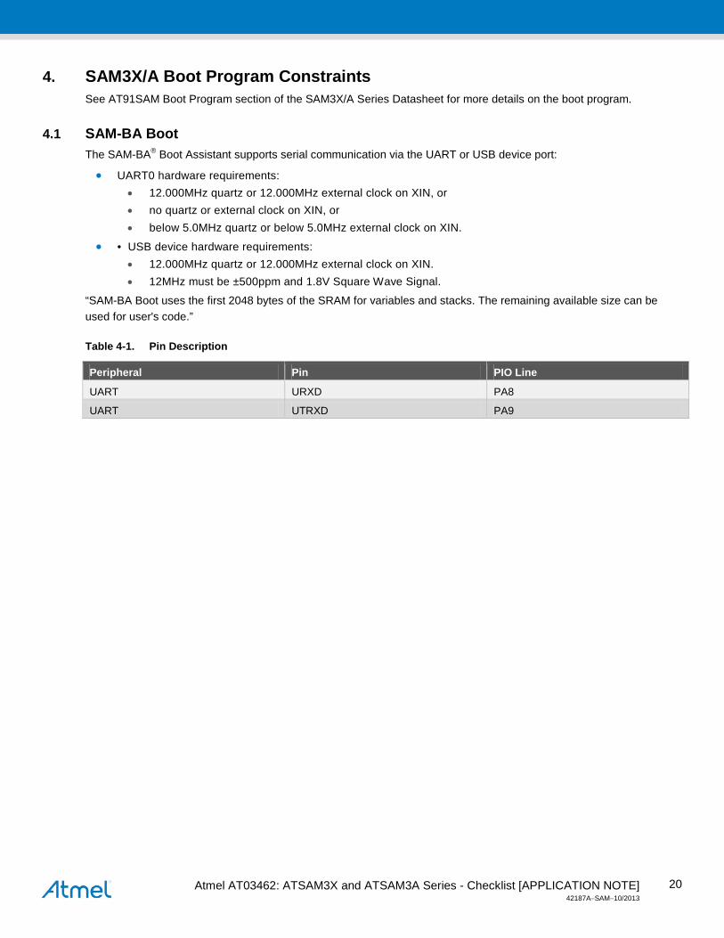
Table 4-1. Pin Description
Peripheral Pin PIO Line
UART URXD PA8
UART UTRXD PA9
Atmel AT03462: ATSAM3X and ATSAM3A Series - Checklist [APPLICATION NOTE] 42187A−SAM−10/2013
21
5. Suggested Reading
5.1 Device Datasheet The device datasheet contains block diagrams of the peripherals and details about implementing firmware for the device. It also contains the electrical specifications and expected characteristics of the device.
The datasheet is available on http://www.atmel.com/ in the Datasheets section of the product page.
5.2 Evaluation Kit User Guide The SAM3X-EK user guide contains schematics that can be used as a starting point when designing with the SAM3X devices. This user guide is available on http://www.atmel.com/ in the documents section of the SAM3X-EK page.
5.3 USB Specification The Universal Serial Bus specification is available from http://www.usb.org.
5.4 USB High Speed Design Guidelines In order to facilitate hardware design around the SAM3 USB On-The-Go High Speed Port, Atmel provides an application note on www.atmel.com.
5.5 ARM Documentation on Cortex-M3 Core • Cortex-M3 Devices Generic User Guide
• Cortex-M3 Technical Reference Manual
These documents are available at http://www.arm.com/ in the info center section.
Atmel AT03462: ATSAM3X and ATSAM3A Series - Checklist [APPLICATION NOTE] 42187A−SAM−10/2013
22
6. Revision History Doc. Rev. Date Comments
42187A 10/2013 Initial document release
Atmel Corporation 1600 Technology Drive San Jose, CA 95110 USA Tel: (+1)(408) 441-0311 Fax: (+1)(408) 487-2600 www.atmel.com
Atmel Asia Limited Unit 01-5 & 16, 19F BEA Tower, Millennium City 5 418 Kwun Tong Road Kwun Tong, Kowloon HONG KONG Tel: (+852) 2245-6100 Fax: (+852) 2722-1369
Atmel Munich GmbH Business Campus Parkring 4 D-85748 Garching b. Munich GERMANY Tel: (+49) 89-31970-0 Fax: (+49) 89-3194621
Atmel Japan G.K. 16F Shin-Osaki Kangyo Building 1-6-4 Osaki, Shinagawa-ku Tokyo 141-0032 JAPAN Tel: (+81)(3) 6417-0300 Fax: (+81)(3) 6417-0370
© 2013 Atmel Corporation. All rights reserved. / Rev.: 42187A−SAM−10/2013
Atmel®, Atmel logo and combinations thereof, Enabling Unlimited Possibilities®, SAM-BA®, and others are registered trademarks or trademarks of Atmel Corporation or its subsidiaries. ARM® and Cortex® are registered trademarks of ARM Ltd. Other terms and product names may be trademarks of others.
Disclaimer: The information in this document is provided in connection with Atmel products. No license, express or implied, by estoppel or otherwise, to any intellectual property right is granted by this document or in connection with the sale of Atmel products. EXCEPT AS SET FORTH IN THE ATMEL TERMS AND CONDITIONS OF SALES LOCATED ON THE ATMEL WEBSITE, ATMEL ASSUMES NO LIABILITY WHATSOEVER AND DISCLAIMS ANY EXPRESS, IMPLIED OR STATUTORY WARRANTY RELATING TO ITS PRODUCTS INCLUDING, BUT NOT LIMITED TO, THE IMPLIED WARRANTY OF MERCHANTABILITY, FITNESS FOR A PARTICULAR PURPOSE, OR NON-INFRINGEMENT. IN NO EVENT SHALL ATMEL BE LIABLE FOR ANY DIRECT, INDIRECT, CONSEQUENTIAL, PUNITIVE, SPECIAL OR INCIDENTAL DAMAGES (INCLUDING, WITHOUT LIMITATION, DAMAGES FOR LOSS AND PROFITS, BUSINESS INTERRUPTION, OR LOSS OF INFORMATION) ARISING OUT OF THE USE OR INABILITY TO USE THIS DOCUMENT, EVEN IF ATMEL HAS BEEN ADVISED OF THE POSSIBILITY OF SUCH DAMAGES. Atmel makes no representations or warranties with respect to the accuracy or completeness of the contents of this document and reserves the right to make changes to specifications and products descriptions at any time without notice. Atmel does not make any commitment to update the information contained herein. Unless specifically provided otherwise, Atmel products are not suitable for, and shall not be used in, automotive applications. Atmel products are not intended, authorized, or warranted for use as components in applications intended to support or sustain life.
![Atmel | SMART SAM G55 Introductionww1.microchip.com/downloads/en/AppNotes/Atmel-42392-SAM-G5… · SAM G55 Schematic Checklist [APPLICATION NOTE] 5 Atmel-42392C-SAM-G55-Schematic-Checklist-ApplicationNote_042016](https://img.pdfslide.net/doc/110x75/5f94c2484d0fb112ec370573/atmel-smart-sam-g55-sam-g55-schematic-checklist-application-note-5-atmel-42392c-sam-g55-schematic-checklist-applicationnote042016.jpg)


![Atmel SAM4L Features Introductionww1.microchip.com/downloads/en/DeviceDoc/Atmel... · ATSAM4L-EK User Guide [APPLICATION NOTE] Atmel-42026F-ATSAM4L-EK-User-Guide-ApplicationNote_082014](https://img.pdfslide.net/doc/110x75/6047f178e1f3ef03307425c7/atmel-sam4l-features-atsam4l-ek-user-guide-application-note-atmel-42026f-atsam4l-ek-user-guide-applicationnote082014.jpg)