Embed Size (px)
Citation preview
APPLICATION NOTE
User Guide for Atmel ATA6870 and Atmel ATmega32HVBEvaluation Kit Hardware
ATA6870-DK10
Features
● Evaluation of Atmel® ATA6870
● Monitoring of 12 battery cells
● Monitoring:● Overvoltage (every cell)● Undervoltage (every cell)● Overheating● Overcurrent
● Open clamp detection
● 12-bit battery cell measurement
● 12-bit temperature measurement
● Controlling of charge/discharge FETs
● Status LEDs for easy evaluation
● Charge balancing
● Coulomb counting for SOC determination
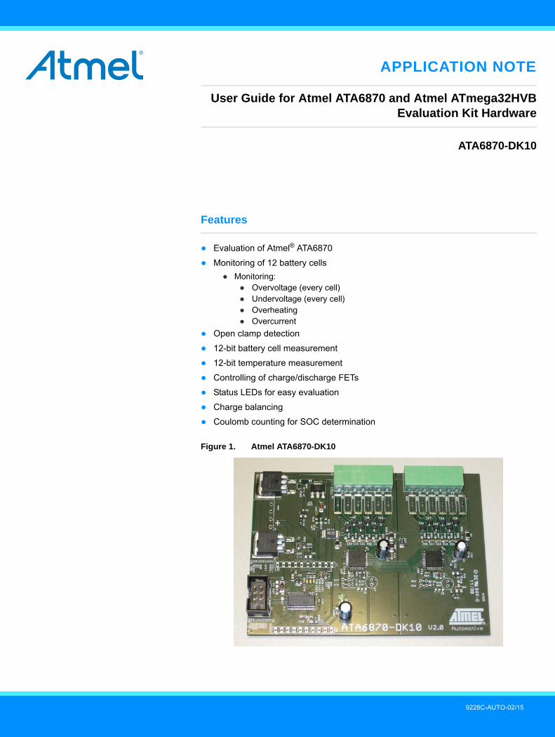
Figure 1. Atmel ATA6870-DK10
9228C-AUTO-02/15
1. Introduction
The Atmel® ATA6870-DK10 is a demonstration board for the Atmel ATA6870, which offers an easy way to start evaluation of battery applications using the Atmel ATmega32HVB in combination with the Atmel ATA6870. The included software demonstrates implementation of a 12 Cell Battery Management System. The supplied code serves as an example of how to use the Atmel ATMega32HVB and Atmel ATA6870 together. The example is not a complete application intended for use with smart batteries, and it is best to use the devices in a slightly different way in a smart battery application.
2. Safety Precautions When Using Li-ion Batteries
Please observe the safety guidelines supplied with the batteries. If improperly used or defective, li-ion and polymer batteries and packs may explode and cause a fire.
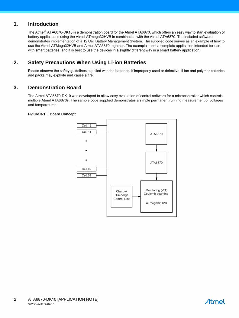
3. Demonstration Board
The Atmel ATA6870-DK10 was developed to allow easy evaluation of control software for a microcontroller which controls multiple Atmel ATA6870s. The sample code supplied demonstrates a simple permanent running measurement of voltages and temperatures.
Figure 3-1. Board Concept
ATA6870
Cell 12
Cell 11
ATA6870
Monitoring (V,T)Coulomb counting
ATmega32HVB
Charge/Discharge
Control Unit
Cell 02
Cell 01
ATA6870-DK10 [APPLICATION NOTE]9228C–AUTO–02/15
2
3.1 System Start
Follow these steps to launch the system.
3.1.1 Installing the Hardware
● Connect the load/charger to be powered between pack+ and pack- on J1
● For demonstration purposes it is possible to use a resistor to simulate a load
● Connect the battery cell stack to the screw connectors on the demonstration board
● Led 1 indicates the enabled status of the demonstration board (controlled by microcontroller SW)
● In case of emulating cells such as a voltage divider, apply sufficient voltage (see Section 3.3 “Powering the Board” on page 5)
3.1.2 Number of Cells
It is possible to run the board with a reduced number of cells. The minimum voltage for each IC is 6.9V. Cell 1 and cell 6 (MBAT) have to be connected. The missing cells should be connected to the upper cell potential of the module. For further information refer to the Atmel ATA6870 datasheet Section 7.3: Reduced Number of Battery Cells Configuration. For the voltage range see Section 3.3 “Powering the Board” on page 5. If fewer than 6 cells are used per IC, the config.h file should be adjusted (CELLSIC# under General Setting). See Section 4.1 “Supplied Code” on page 7 for further information on how to configure the supplied software correctly.
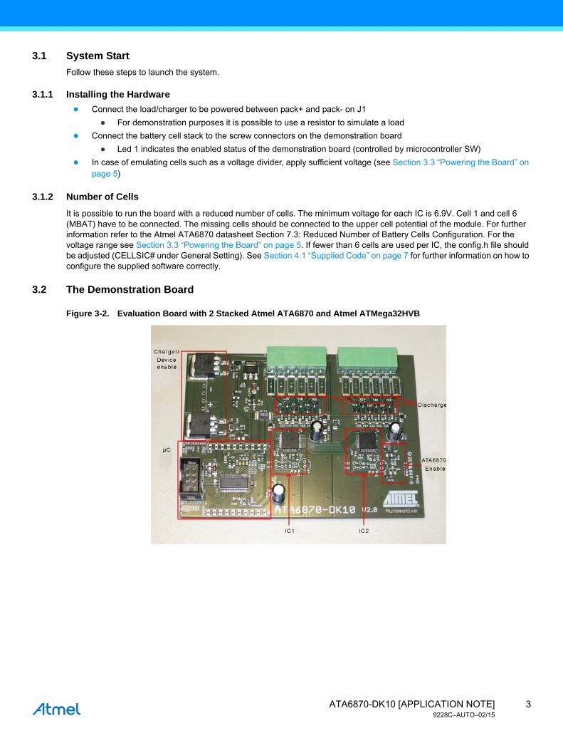
3.2 The Demonstration Board
Figure 3-2. Evaluation Board with 2 Stacked Atmel ATA6870 and Atmel ATMega32HVB
3ATA6870-DK10 [APPLICATION NOTE]9228C–AUTO–02/15
3.2.1 On-board Features
The demonstration board includes the following items:
● 2 Atmel® ATA6870 QFN 7mm 7mm
● Atmel ATMega32HVB
● 12 external N-channel MOSFETs for balancing of battery cells
● Connectors
● ISP connector for programming/debugging the Atmel ATMega32HVB
● Screw connectors for connecting up to 12 battery cells
J9 should never be set while the Atmel ATmega32HVB is being programmed or while it is entering debug mode. It can be mounted as soon as AVR Studio prompts for additional SPI lines to be connected in debug mode or after the device has been correctly programmed.
Table 3-1. Connector Overview
J7 Function J8 Function
1 CELL- 1 VDDHVM
2 PACK- 2
3 3 VCC
4 VFET 4 GND
5 5 IRQ
6 GND 6 CLK
7 OD 7 MISO
8 OC 8 MOSI
9 RESET 9 SCK
10 GND 10 CS_N
J1 Connector for charger/device to be powered
J2 ISP connector
J3 Upper battery stack (cells 7-12)
J4 Bottom battery stack (cells 1-6)
J9 Jumper to enable/disable MISO line of Atmel ATA6870
ATA6870-DK10 [APPLICATION NOTE]9228C–AUTO–02/15
4
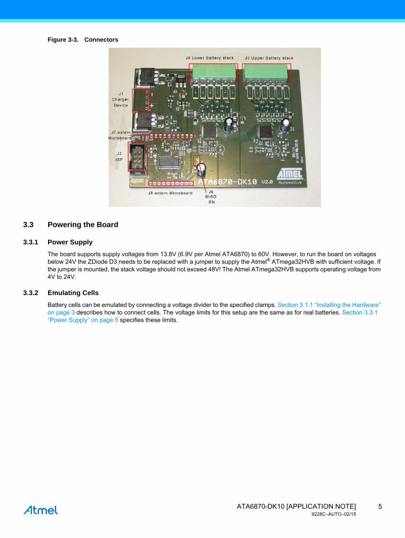
Figure 3-3. Connectors
3.3 Powering the Board
3.3.1 Power Supply
The board supports supply voltages from 13.8V (6.9V per Atmel ATA6870) to 60V. However, to run the board on voltages below 24V the ZDiode D3 needs to be replaced with a jumper to supply the Atmel® ATmega32HVB with sufficient voltage. If the jumper is mounted, the stack voltage should not exceed 48V! The Atmel ATmega32HVB supports operating voltage from 4V to 24V.
3.3.2 Emulating Cells
Battery cells can be emulated by connecting a voltage divider to the specified clamps. Section 3.1.1 “Installing the Hardware” on page 3 describes how to connect cells. The voltage limits for this setup are the same as for real batteries. Section 3.3.1 “Power Supply” on page 5 specifies these limits.
5ATA6870-DK10 [APPLICATION NOTE]9228C–AUTO–02/15
4. Software Description: Monitoring of Up to 12 Battery Cells
The supplied code is documented and easy to adjust for verifying the functions of the Atmel® ATA6870 and start BMS application development work.
After the board has been connected as described above the microcontroller automatically starts a cyclic measurement of voltages, temperature, and current. LED 1 indicates these cyclic measurements. It toggles in default operation. A continuously illuminated LED1 indicates an open clamp. See Section 4.2 “Open Cell Check” on page 7 for more information about open clamp detection. LED 2 indicates that for some reason the MOSFETS have been disabled. The default software disables the FETs in case of these events:
● Overvoltage (at least 1 cell exceeds the upper default threshold of 4.2V)
● Undervoltage (at least 1 cell exceeds the lower default threshold of 2.5V)
● Overcurrent (the current through the shunt exceeds the default threshold of 80mA)
● Overheating (the temperature exceeds the upper threshold, default value is 60°C)
● Low temperature threshold (the default threshold is -20°C)
LED 3 indicates whether the Atmel ATA6870s are turned on or not. An active LED indicates that the Atmel ATA6870s are enabled.
The Atmel ATmega32HVB has no clock divider to provide an external slower clock than 1/2 CPU clock. Requirement of Atmel ATA6870 is fCLK > 2 fSPI. Hence, the clock frequency of 1MHz is mandatory to provide a 500kHz clock for the ADCs of the Atmel ATA6870 and 250kHz for SPI.
Table 4-1. LED Functions
LED Function
LED 1Indicates clamp is open when permanently illuminatedIndicates cyclic measurements when blinking
LED 2 On indicates disabled MOSFETs for one of the reasons listed above
LED 3 On indicates active Atmel ATA6870
ATA6870-DK10 [APPLICATION NOTE]9228C–AUTO–02/15
6
4.1 Supplied Code
4.1.1 config.h
This section refers to the config.h file provided in the zip archive with this Application Note. Only values in the User Setting paragraph should be changed!
------------- GENERAL SETTING--------------------------------CELLSIC# Selecting which Cells are used Bits 0-5 -> Cells 1-6------------- TEMPERATURE SETTING----------------------------RES_REF# Value of the mounted reference resistor (default: 3300)T_TLS Temperature belonging to the first Value in the lookup
table (index 0, default: -20)T_TLE Temperature belonging to the last value in the lookup
table (default: 80)T_TLSZ Temperature step size used in the lookup table (default: 1)T_LOWERTHRESHOLD Lower temperature thresholdT_UPPERTHRESHOLD Upper temperature threshold ------------- COULOMBCOUNTER SETTING-------------------------SHUNT_RESISTANCE Value of the shunt resistor in mOhmRCC_CONVERSIONPERIOD The cycle times for the Regular Current Check
0x00 - 256ms (default)0x01 - 512ms 0x02 - 1s
0x11 - 2sRCC_DIVIDEDSZ 0x01 to enable divided Voltage (Current) stepsizeRCC_CHARGETHRESHOLD Threshold for charging current, exceeding the
threshold will turn off the MosfetsRCC_DISCHARGETHRESHOLD Threshold for discharging current, exceeding the
threshold will turn off the Mosfets
Other values should not be changed in the default HW setup!
4.2 Open Cell Check
The implemented function checks for open clamps by measuring the cell voltages two times. During the first check a normal measurement is completed and the values stored. During the second check the voltages are measured while the discharge function for all cells is active. If the two measurements for the same cell differ by more than 100mV it is very likely that one or more cells are not properly connected. The implemented method cannot be used to determine which cell is not properly connected. A continuously illuminated LED1 indicates an open clamp.
4.3 Voltage Measurements
The standard software loop measures the voltage ADC value and the offset ADC value for every cell and checks for overvoltage and undervoltage once per cycle. Further information about the acquiring of voltages can be found in the Atmel® ATA6870 datasheet Section 7.5.1. The formula for calculating the voltage:
Voltage (Cell) 4VVacq Voffset–
3031 Voffset–--------------------------------- =
7ATA6870-DK10 [APPLICATION NOTE]9228C–AUTO–02/15
4.4 Temperature Measurements
The default software only measures channel 1 of chip 1. The temperature sensors are based on a resistor divider using a standard resistor and an NTC resistor. This resistor divider is connected to the reference of the ADC for temperature measuring. Because the ADC is sharing the same reference value, the output of temperature measurement with ADC is ratio metric. Further information is found in the Atmel ATA6870 datasheet Section 7.5.3: Temperature Channel.
For this application Atmel recommends using Res_Ref1 = 3.3k and RES_NTC1 R25 = 10k, B = 3435. The software supplied for this board uses these values as default. The function uses a lookup table to determine the temperature. This table has to be edited if an NTC other than the recommended one is used. The values in the lookup table range from –20°C (index 0) to +80°C (index 100). These values can be edited via the config.h file in the User Settings section. More Information about this file can be found in Section 4.1 “Supplied Code” on page 7. The calculation of RES_NTC is carried out based on the formula provided in the Atmel ATA6870 datasheet Section 7.5.3:
When using another NTC, the LookupADC.txt has to be edited to match the NTC used.
4.5 State of Charge Measurements
Highly precise SOC measurement is possible by combining the features of the Atmel ATmega32HVB and the Atmel ATA6870. The coulomb counting feature of the Atmel ATmega32HVB enables highly precise measurements of the change in the state of charge. Frequent reading of the current in a shunt is used to update the SOC frequently. The acquired cell voltages and temperatures can be used to determine the SOC without the Atmel ATmega32HVB. The easiest way is to compare the SOC measured by the added/extracted charge with the calculated SOC using the cell voltage, temperature, and the data provided by the manufacturer of the cells. Further information regarding the coulomb counting ADC as well as an implementation suitable for the Atmel ATmega16HVA is found in Application Note AVR352.
4.6 Overcurrent Protection
The current through the shunt is calculated by measured voltage drop. The limit can be set via the CADRDC/CADRCC register. The step size depends on the settings of the CADCSRC register and the shunt used. For further information about limiting current see the Atmel ATmega32HVB datasheet Section 19.4: Regular Current Detection Operation. The supplied software allows the feature to be tested by adjusting the values in the config.h file. More Information about this file can be found in Section 4.1 “Supplied Code” on page 7. Values/part of the code should only be changed if you are aware of possible consequences. The default implementation continuously measures the current and generates an interrupt if the entered thresholds are exceeded. The thresholds are defined in the config.h file. The thresholds are written to the registers in the function CCinit in the Atmel ATA6870_func.c file. Refer to the features of the Atmel ATmega32HVB in the coulomb counter section to learn more about the time the controller waits for the values to be written.
adc (out) 2048 1RES_NTC(1)
(RES_NTC(1) + RES_REF(1))--------------------------------------------------------------------------- 8
15------ 8
10------–+
=
C Code Example
CADRCC = RCC_CADRCC;while(CADCSRA & (1 << CADUB));CADRDC = RDC_CADRDC;while(CADCSRA & (1 << CADUB));
// Charge Threshold// Wait values to be written// Discharge Threshold// Wait values to be written
ATA6870-DK10 [APPLICATION NOTE]9228C–AUTO–02/15
8
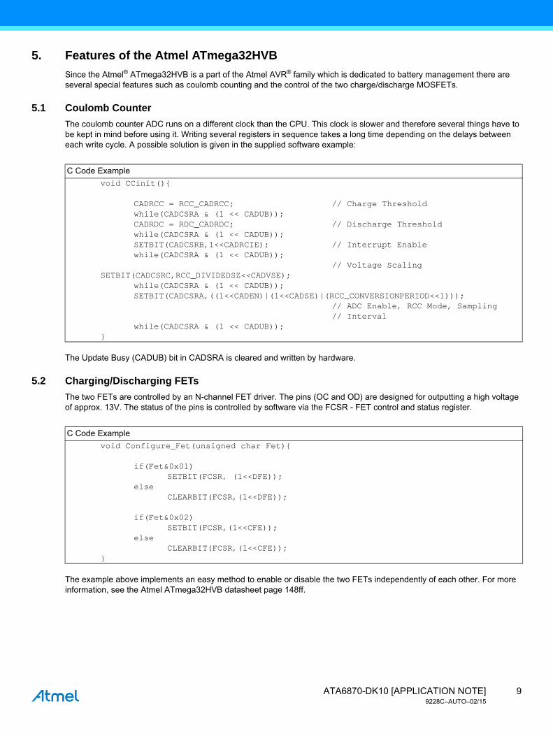
5. Features of the Atmel ATmega32HVB
Since the Atmel® ATmega32HVB is a part of the Atmel AVR® family which is dedicated to battery management there are several special features such as coulomb counting and the control of the two charge/discharge MOSFETs.
5.1 Coulomb Counter
The coulomb counter ADC runs on a different clock than the CPU. This clock is slower and therefore several things have to be kept in mind before using it. Writing several registers in sequence takes a long time depending on the delays between each write cycle. A possible solution is given in the supplied software example:
The Update Busy (CADUB) bit in CADSRA is cleared and written by hardware.
5.2 Charging/Discharging FETs
The two FETs are controlled by an N-channel FET driver. The pins (OC and OD) are designed for outputting a high voltage of approx. 13V. The status of the pins is controlled by software via the FCSR - FET control and status register.
The example above implements an easy method to enable or disable the two FETs independently of each other. For more information, see the Atmel ATmega32HVB datasheet page 148ff.
C Code Example
void CCinit(){
CADRCC = RCC_CADRCC;while(CADCSRA & (1 << CADUB));CADRDC = RDC_CADRDC;while(CADCSRA & (1 << CADUB));SETBIT(CADCSRB,1<<CADRCIE);while(CADCSRA & (1 << CADUB));
SETBIT(CADCSRC,RCC_DIVIDEDSZ<<CADVSE);while(CADCSRA & (1 << CADUB));
// Charge Threshold
// Discharge Threshold
// Interrupt Enable
// Voltage Scaling
SETBIT(CADCSRA,((1<<CADEN)|(1<<CADSE)|(RCC_CONVERSIONPERIOD<<1)));
while(CADCSRA & (1 << CADUB));}
// ADC Enable, RCC Mode, Sampling // Interval
C Code Example
void Configure_Fet(unsigned char Fet){
if(Fet&0x01)SETBIT(FCSR, (1<<DFE));
elseCLEARBIT(FCSR,(1<<DFE));
if(Fet&0x02)SETBIT(FCSR,(1<<CFE));
elseCLEARBIT(FCSR,(1<<CFE));
}
9ATA6870-DK10 [APPLICATION NOTE]9228C–AUTO–02/15
6. Power Consumption
There are several ways to reduce the power consumption of the Atmel ATA6870 and the Atmel ATmega32HVB. Sleep modes are documented in the datasheet of the Atmel ATA6870 Section 7.1.1 and in the Atmel ATmega32HVB datasheet Section 10. This board allows the Atmel ATA6870 to be enabled/disabled using the Atmel ATmega32HVB software. The pin PB2 is used to control a transistor for activating/deactivating the Atmel ATA6870. Other options which are not implemented are the use of interrupts and a timer (sleep between cycles).
ATA6870-DK10 [APPLICATION NOTE]9228C–AUTO–02/15
10
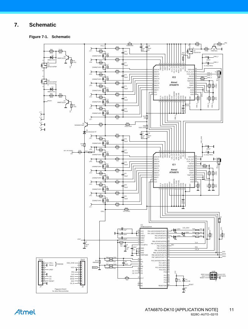
7. Schematic
Figure 7-1. Schematic
R59
1kΩR34
100Ω
DISCH5 MB
AT6
OD
MB
AT7
VD
DH
VIR
Q_I
NC
LK_O
UT
CS
_N_O
UT
SC
K_O
UT
MO
SI_
OU
T
CS
_N13 14 15 16 17 18 19 20 21 22 23 24
48 47 46 45 44 43 42 41 40 39 38 37
SC
KM
OS
IM
ISO
MFI
RS
TD
TST
SC
AN
MO
DE
CS
_FU
SE
VD
DFU
SE
DV
SS
DV
DD
GN
D
GN
D
DIS
CH
6
MIS
O_I
NP
D_N
VD
DH
VP
123456789
10
1211
MBAT5DISCH4MBAT4DISCH3MBAT3DISCH2MBAT2
MBAT1DISCH1
IC2
AtmelATA6870
IRQCLK
36123
J50Ω
D
S
G
3534333231302928272625
VDDHVMPD_N_OUTPOW_ENA
PWTSTBIASRES
TEMPREFTEMP2TEMP1
TEMPVSSAVSSAVDDATST
R40
C6
51kΩ
nc (33μF/50V)+
Q6FMMT620
121kΩ
GND_2GND_2GND_2
GND_2
GND_2
R55
R38
7.5kΩ
R4
10Ω/0.25W
R41 PB2
4.7kΩ
R58
1kΩ
R45
1kΩ
R46
1kΩ
R96
D2
MM3Z13VC
56kΩ
R109
56kΩ
R93
56kΩ
PACK+
R94
56kΩ
T18
ZXMN2F34FH
CELL+
CELL-
J3-7
R30
100Ω T14
ZXMN2F34FH
R33
100Ω T17
ZXMN2F34FH
R32
100Ω T16
ZXMN2F34FH
R31
100Ω
R29
100Ω T15
ZXMN2F34FH
T13
ZXMN2F34FH
J3-6
J3-5
J3-4
J3-3
J3-2
J3-1
J1-3
R270Ω
R8610Ω/0.25W
C3+
10μF30V
C19
100nF30V
C8
2.2μF25V
C5
100nF50V
C1+
10μF30V
C32
100nF30V
R39
10Ω/0.25W
R12
tbd
R37150Ω
R144.7kΩ
R104.7kΩ
D4LL4148
C10
100nF
Q7SQ2301ES
Q5IRF5210SPBF
Q4IRF5210SPBF
C33
10nF
R66
100k
Ω
C38
220nF
C11
100nF
C12
100nF
C13
100nF
C14
100nF
C15
100nF
GN
D_2
GN
D_2
GN
D_2
GN
D_2
GN
D_2
R49
R57
3.3k
kΩ
3.3k
kΩ
R52
R56
NTC
NTC
R47
1kΩ
R53
1kΩ
R54
1kΩ
R25
1kΩ
R190Ω
R11
100Ω
D1
D
G
G
S
S
D
MM3Z13VC
DISCH5 MB
AT6
MB
AT7
VD
DH
VIR
Q_I
NC
LK_O
UT
CS
_N_O
UT
SC
K_O
UT
MO
SI_
OU
T
CS
_N13 14 15 16 17 18 19 20 21 22 23 24
48 47 46 45 44 43 42 41 40 39 38 37
SC
KM
OS
IM
ISO
MFI
RS
TD
TST
SC
AN
MO
DE
CS
_FU
SE
VD
DFU
SE
DV
SS
DV
DD
GN
D
GN
D
DIS
CH
6
MIS
O_I
NP
D_N
VD
DH
VP
123456789
10
1211
MBAT5DISCH4MBAT4DISCH3MBAT3DISCH2MBAT2
MBAT1DISCH1
IC1
AtmelATA6870
IRQCLK
LED1
J9
PB2
RESET
CLK
SCKMOSIMISO
IRQCS_N
LED_0603
LED3
LED2
36123
J60Ω
3534333231302928272625
7
PA1 (ADC1/SGND/PCINT1)PA2 (PCINT2/T0)PA3 (PCINT3/T1)
PB0 (PCINT4/ICP00)
PB2 (PCINT6)
VCC
IC3ATMEGA32HVB
VCCVREGVREFVFET
PB3 (PCINT7)PB4 (SS/PCINT8)
PB5 (SCK/PCINT9)
PB1 (PCINT5/CKOUT)
PA0 (ADC0/SGND/PCINT1)8910
1436
64
121311
51535
3
4443
12
4218
OCOD
16
37
1727
2021222324252628
293031
246
VCC
3x2M
MOSIMISOSCK
RESET
J2
135
323334
41403938
19
VDDHVMPD_N_OUTPOW_ENA
PWTSTBIASRES
TEMPREFTEMP2TEMP1
TEMPVSSAVSSAVDDATST
C7
nc (33μF/50V)+
+
121kΩ
R21
R24
1kΩR18
nc
opt. ext.supply
TP1
R3
1kΩ
R5
1kΩ
T12
ZXMN2F34FH
Q2MMBT2222A
OC
J1-2
J1-1
J1-4
R954.7kΩ
Q1MMBT2222A
Q2NSS60601MZ4
D3BZV55C6V8-TP
J4-7
R6
100Ω T8
ZXMN2F34FH
R10
R22 nc 100Ω T11
ZXMN2F34FH
R9
100Ω T10
ZXMN2F34FH
R8
100Ω
R1
100Ω
R2
1kΩ
T9
ZXMN2F34FH
T7
ZXMN2F34FH
J4-6
J4-5
J4-4
J4-3
J4-2
J4-1
C16
100nF
C20
10nF
R44
100k
Ω
R17
5.1k
Ω
C24
C24
nc
220nFC17
100nF
C18
100nF
C21
100nF
C22
100nF
C23
100nFV
DD
_HV
M
VC
C
VC
C
R20
5.1k
Ω
VC
C
R13
R23
3.3k
Ω
3.3k
Ω
R77
R76
NTC
NTC
R7
1kΩ
R15
1kΩ
R16
C30 100nF
C27
100nF
C31
C34
100nF
100nF
C2 2.2μF
1kΩ
100ΩR89
R113RSENSE 1kΩR99
100ΩR91
1kΩR100PACK-
VFET
R881kΩ
R28 1kΩ
R35 1kΩ
R36 1kΩ
R26
10/0.25WΩ
PB6 (MOSI/PCINT10)PB7 (MISO/PCINT11)
PC0 (INT0/EXTPROT)PC1 (INT1)PC2 (INT2)
PC4 (SCL)PC5
PV1PV2PV3PV4
RESET/DW
PC3 (INT3/SDA)
BATTVCLMP10
GNDGNDGND
PIPPININNI
1CELL-
RSENSE
10x1F
J7
10x1F
J8Piggypack Board
for other Microcontroller
VDD_HVM
VCC
CLKIRQ
CS_NSCK
MOSIMISO
PACK-
VFET
ODOCRESET
2345678910
NVOCOD
PVT
NCNC
VREFGND
123456789
10
11ATA6870-DK10 [APPLICATION NOTE]9228C–AUTO–02/15
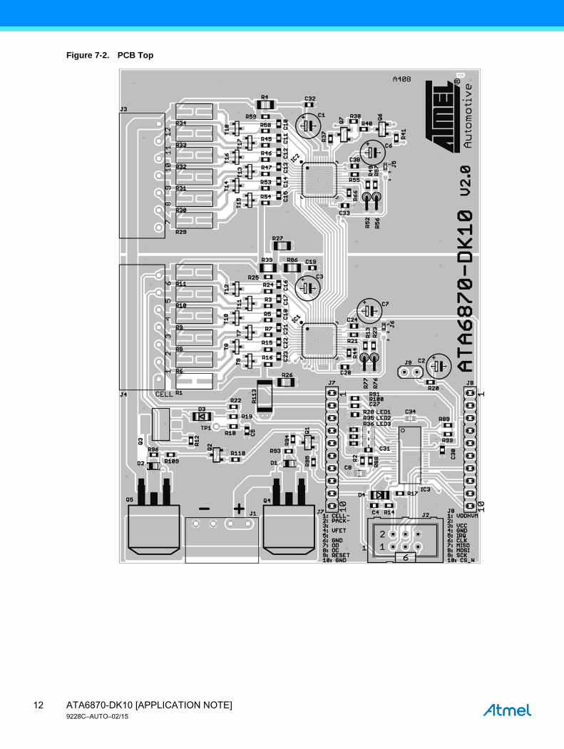
Figure 7-2. PCB Top
ATA6870-DK10 [APPLICATION NOTE]9228C–AUTO–02/15
12
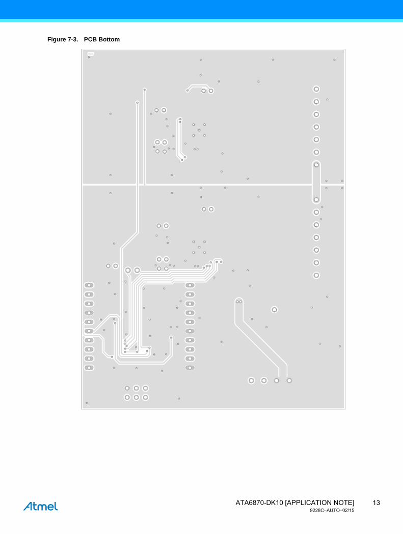
Figure 7-3. PCB Bottom
13ATA6870-DK10 [APPLICATION NOTE]9228C–AUTO–02/15
8. Revision History
Please note that the following page numbers referred to in this section refer to the specific revision mentioned, not to this document.
Revision No. History
9228C-AUTO-02/15 Put document in the latest template
9228B-AUTO-10/12 Section 4.4 “Temperature Measurements” on page 8 updated
ATA6870-DK10 [APPLICATION NOTE]9228C–AUTO–02/15
14
XX X XX XAtmel Corporation 1600 Technology Drive, San Jose, CA 95110 USA T: (+1)(408) 441.0311 F: (+1)(408) 436.4200 | www.atmel.com
© 2015 Atmel Corporation. / Rev.: 9228C–AUTO–02/15
Atmel®, Atmel logo and combinations thereof, Enabling Unlimited Possibilities®, AVR®, and others are registered trademarks or trademarks of Atmel Corporation in U.S. and other countries. Other terms and product names may be trademarks of others.
DISCLAIMER: The information in this document is provided in connection with Atmel products. No license, express or implied, by estoppel or otherwise, to any intellectual property rightis granted by this document or in connection with the sale of Atmel products. EXCEPT AS SET FORTH IN THE ATMEL TERMS AND CONDITIONS OF SALES LOCATED ON THEATMEL WEBSITE, ATMEL ASSUMES NO LIABILITY WHATSOEVER AND DISCLAIMS ANY EXPRESS, IMPLIED OR STATUTORY WARRANTY RELATING TO ITS PRODUCTSINCLUDING, BUT NOT LIMITED TO, THE IMPLIED WARRANTY OF MERCHANTABILITY, FITNESS FOR A PARTICULAR PURPOSE, OR NON-INFRINGEMENT. IN NO EVENTSHALL ATMEL BE LIABLE FOR ANY DIRECT, INDIRECT, CONSEQUENTIAL, PUNITIVE, SPECIAL OR INCIDENTAL DAMAGES (INCLUDING, WITHOUT LIMITATION, DAMAGESFOR LOSS AND PROFITS, BUSINESS INTERRUPTION, OR LOSS OF INFORMATION) ARISING OUT OF THE USE OR INABILITY TO USE THIS DOCUMENT, EVEN IF ATMEL HASBEEN ADVISED OF THE POSSIBILITY OF SUCH DAMAGES. Atmel makes no representations or warranties with respect to the accuracy or completeness of the contents of thisdocument and reserves the right to make changes to specifications and products descriptions at any time without notice. Atmel does not make any commitment to update the informationcontained herein. Unless specifically provided otherwise, Atmel products are not suitable for, and shall not be used in, automotive applications. Atmel products are not intended,authorized, or warranted for use as components in applications intended to support or sustain life.
SAFETY-CRITICAL, MILITARY, AND AUTOMOTIVE APPLICATIONS DISCLAIMER: Atmel products are not designed for and will not be used in connection with any applications wherethe failure of such products would reasonably be expected to result in significant personal injury or death (“Safety-Critical Applications”) without an Atmel officer's specific writtenconsent. Safety-Critical Applications include, without limitation, life support devices and systems, equipment or systems for the operation of nuclear facilities and weapons systems.Atmel products are not designed nor intended for use in military or aerospace applications or environments unless specifically designated by Atmel as military-grade. Atmel products arenot designed nor intended for use in automotive applications unless specifically designated by Atmel as automotive-grade.
![Atmel AT06409: DALI Master with ATxmega32E5 User Guideww1.microchip.com/downloads/en/DeviceDoc/atmel... · Atmel AT06409: DALI Master with ATxmega32E5 User Guide [APPLICATION NOTE]](https://img.pdfslide.net/doc/110x75/5f18936e586a3c0a1560e8ae/atmel-at06409-dali-master-with-atxmega32e5-user-atmel-at06409-dali-master-with.jpg)


![Atmel-ICE (USER GUIDE) - 秋月電子通商 - 電子部品・ …akizukidenshi.com/.../Atmel-42330-Atmel-ICE_UserGuide.pdf9. Atmel-ICE [USER GUIDE] 42330A-MCU-07/2014 3 7. Command](https://img.pdfslide.net/doc/110x75/5ad0b8667f8b9ad24f8dff11/atmel-ice-user-guide-atmel-ice-user.jpg)
![Atmel SAM C20 QTouch Safety Library User Guide...Atmel SAM C20 Safety Library [USER GUIDE] Atmel-42679C-SAM-C20-QTouch-Safety-Library_User Guide-07/2016 9 Figure 2-4. API Usage Yes](https://img.pdfslide.net/doc/110x75/60b1328d4317f551c152eff4/atmel-sam-c20-qtouch-safety-library-user-guide-atmel-sam-c20-safety-library.jpg)


![Atmel-ICE (USER GUIDE) - RS Components · Atmel-ICE [USER GUIDE] 42330A-MCU-07/2014 4 1. Introduction 1.1 Introduction to the Atmel-ICE Atmel-ICE is a powerful development tool for](https://img.pdfslide.net/doc/110x75/5f61277fe3b3c12ba643c824/atmel-ice-user-guide-rs-components-atmel-ice-user-guide-42330a-mcu-072014.jpg)

![Atmel AVR2054: Serial Bootloader User Guideww1.microchip.com/downloads/en/AppNotes/Atmel-8390...Atmel AVR2054: Serial Bootloader User Guide [APPLICATION NOTE] 8390D−WIRELESS−03/2015](https://img.pdfslide.net/doc/110x75/5ecc43c2e2e77955c85a5805/atmel-avr2054-serial-bootloader-user-atmel-avr2054-serial-bootloader-user.jpg)


![Atmel-ICE (USER GUIDE) - cdn-reichelt.de · Atmel-ICE [USER GUIDE] 42330A-MCU-07/2014 6 2. Getting Started with the Atmel-ICE 2.1 Full Kit Contents The Atmel-ICE full kit contains](https://img.pdfslide.net/doc/110x75/5e15ed0a41d34769f84a95f1/atmel-ice-user-guide-cdn-atmel-ice-user-guide-42330a-mcu-072014-6-2-getting.jpg)