Embed Size (px)
Citation preview
Atmel AVR1912: Atmel XMEGA-B1 Xplained Hardware User Guide
Features • Atmel® ATxmega128B1 microcontroller • 4x40 transflective LCD module with backlight • One USB full/low speed device interface • Analog input (to ADC)
- Light sensor - Temperature sensor - External voltage input - Potentiometer voltage
• Digital I/O - Four Atmel QTouch® buttons - Four user LEDs - One power LED - Four expansion headers
• Footprints for external memory - Atmel AT45DB series DataFlash® serial flash - Atmel AT25DF series industry standard serial flash
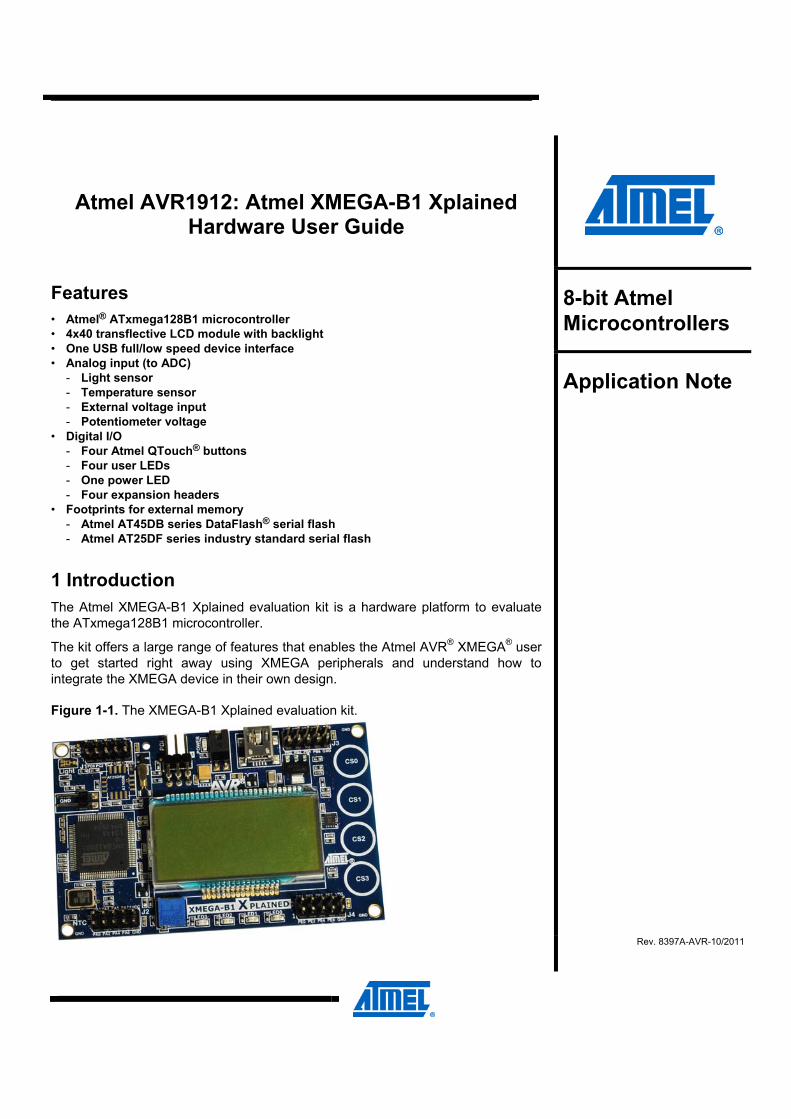
1 Introduction The Atmel XMEGA-B1 Xplained evaluation kit is a hardware platform to evaluate the ATxmega128B1 microcontroller.
The kit offers a large range of features that enables the Atmel AVR® XMEGA® user to get started right away using XMEGA peripherals and understand how to integrate the XMEGA device in their own design.
Figure 1-1. The XMEGA-B1 Xplained evaluation kit.
8-bit Atmel Microcontrollers Application Note
Rev. 8397A-AVR-10/2011
2 Atmel AVR1912 8397A-AVR-10/2011
2 Related items Atmel AVR Studio® 5 (Atmel free IDE) http://www.atmel.com/dyn/products/tools_card.asp?tool_id=17212
Atmel AVR JTAGICE 3 (on-chip programming and debugging tool) http://www.atmel.com/dyn/products/tools_card.asp?tool_id=17213
Atmel AVR ONE! (on-chip programming and debugging tool) http://www.atmel.com/dyn/products/tools_card.asp?tool_id=4279
Atmel AVR JTAGICE mkII (on-chip programming and debugging tool) http://www.atmel.com/dyn/products/tools_card.asp?tool_id=3353
FLIP (flexible in-system programmer) http://www.atmel.com/dyn/products/tools_card.asp?tool_id=3886
Atmel AVR1912
38397A-AVR-10/2011
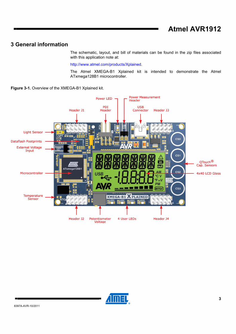
3 General information The schematic, layout, and bill of materials can be found in the zip files associated with this application note at:
http://www.atmel.com/products/Xplained.
The Atmel XMEGA-B1 Xplained kit is intended to demonstrate the Atmel ATxmega128B1 microcontroller.
Figure 3-1. Overview of the XMEGA-B1 Xplained kit.
4 Atmel AVR1912 8397A-AVR-10/2011
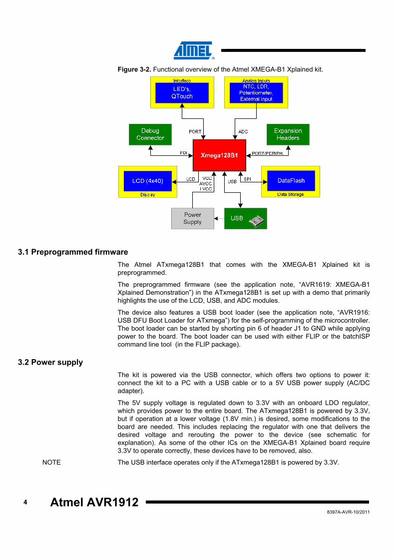
Figure 3-2. Functional overview of the Atmel XMEGA-B1 Xplained kit.
3.1 Preprogrammed firmware The Atmel ATxmega128B1 that comes with the XMEGA-B1 Xplained kit is preprogrammed.
The preprogrammed firmware (see the application note, “AVR1619: XMEGA-B1 Xplained Demonstration”) in the ATxmega128B1 is set up with a demo that primarily highlights the use of the LCD, USB, and ADC modules.
The device also features a USB boot loader (see the application note, “AVR1916: USB DFU Boot Loader for ATxmega”) for the self-programming of the microcontroller. The boot loader can be started by shorting pin 6 of header J1 to GND while applying power to the board. The boot loader can be used with either FLIP or the batchISP command line tool (in the FLIP package).
3.2 Power supply The kit is powered via the USB connector, which offers two options to power it: connect the kit to a PC with a USB cable or to a 5V USB power supply (AC/DC adapter).
The 5V supply voltage is regulated down to 3.3V with an onboard LDO regulator, which provides power to the entire board. The ATxmega128B1 is powered by 3.3V, but if operation at a lower voltage (1.8V min.) is desired, some modifications to the board are needed. This includes replacing the regulator with one that delivers the desired voltage and rerouting the power to the device (see schematic for explanation). As some of the other ICs on the XMEGA-B1 Xplained board require 3.3V to operate correctly, these devices have to be removed, also.
NOTE The USB interface operates only if the ATxmega128B1 is powered by 3.3V.
Atmel AVR1912
58397A-AVR-10/2011
3.3 Measuring Atmel ATxmega128B1 power consumption As part of an evaluation of the ATxmega128B1, it may be of interest to measure its power consumption. The two-pin power measurement header, which has a jumper mounted on it, is the only connection between the common VTG (V_Target) power plane and the VXM (V_Xmega) power plane. By replacing the jumper with an ammeter, it is possible to determine the ATxmega128B1 current consumption. To locate the power measurement header, please refer to Figure 3-1.
WARNING Do not power the board without having the jumper or an ammeter mounted. Otherwise, the device may be damaged.
3.4 Programming the ATxmega128B1 through the USB interface The ATxmega128B1 can be programmed through the USB interface. This can be accomplished using the USB boot loader that is preprogrammed in the device.
The boot loader is evoked by shorting pin 6 on J1 to GND before applying power to the board. A 100mil jumper can be used. Programming is performed through the FLIP plug-in in AVR Studio (which can also be started as a standalone application).
NOTE If any external programming tool is used on the ATxmega128B1, the boot loader might be erased, and it will not be possible to program the device through the USB interface. In this case, the boot loader has to be restored (available on the Atmel website) with an external programming tool.
6 Atmel AVR1912 8397A-AVR-10/2011
4 Connectors The 90° angled, 6-pin, 100mil header is the PDI programming and debugging header for the Atmel ATxmega128B1.
The Atmel XMEGA-B1 Xplained board also has a USB 2.0 mini B connector.
The XMEGA-B1 Xplained board has four 10-pin, 100mil headers. Two of the headers provide a fixed communication interface (J1 and J4). One header provides analog functionality (J2), and the remaining header (J3) provides general purpose digital I/O.
For the location of the respective headers, refer to Figure 3-1.
4.1 Programming and debugging header The Atmel ATxmega128B1 can be programmed and debugged by connecting an external programming and debugging tool to the PDI header. The header has a standard PDI programmer pin-out (refer to online help in AVR Studio), and tools such as the Atmel JTAGICE 3, Atmel AVR ONE!, or Atmel AVR JTAGICE mkII can thus be connected to the PDI header. If it is desired to use PDI for programming and debugging, an adapter must be used:
• (Dark blue) debugWIRE, SPI, PDI, aWire adaptor for JTAGICE 3, ref. A08-0735 • (Green) Standoff adaptor nr.3 JTAG/ISP for AVR ONE!, ref. A08-0254 • (White) XMEGA PDI adaptor for AVR JTAGICE mkII, ref. A09-0412
NOTE The scoring in the board is made to fit the orientation tab on the connector.
Table 4-1. ATxmega128B1 programming and debugging the PDI interface. Pin PDI (1) JTAGICE AVR ONE! JTAGICE mkII
1 PDI_DATA
2 VTG (default 3.3V)
3 (n.c.)
4 (n.c.)
5 PDI_CLOCK
6 GND
debugWIRE, SPI, PDI, aWire
adaptor
ref. A08-0735
Color: dark blue
Standoff adaptor nr.3 JTAG/ISP
ref. A08-0254
Color: green
XMEGA PDI adaptor
ref. A09-0412
Color: white
Note: 1. Standard pin-out for Atmel programming tools.
Table 4-2. Atmel programming and debugging tool interfaces. JTAGICE 3, AVRONE!
10-pin header PDI signal
Squid cable colors
PDI signal JTAGICE mkII 10-pin header
Pin 1 TCK Black (0) TCK Pin 1
Pin 2 GND GND White (1) GND GND Pin 2
Pin 3 TDO PDI_DATA Grey (2) TDO Pin 3
Pin 4 VTref VTG (default 3.3V) Purple (3)
VTG (default 3.3V) VTref Pin 4
Pin 5 TMS Blue (4) TMS Pin 5
Pin 6 nSRST PDI_CLOCK Green (5) PDI_CLOCK nSRST Pin 6
Pin 7 (n.c.) Yellow (6) (n.c.) Pin 7
Atmel AVR1912
78397A-AVR-10/2011
JTAGICE 3, AVRONE!
10-pin header PDI signal
Squid cable colors
PDI signal JTAGICE mkII 10-pin header
Pin 8 nTRST Orange (7) nTRST Pin 8
Pin 9 TDI Red (8) PDI_DATA TDI Pin 9
Pin 10 GND Brown (9) GND Pin 10
NOTE The device also features a JTAG port for programming and debugging. To optimize the onboard I/O management, the JTAG pin allocation (PB[7:4]) is used to drive the user LEDs. The JTAG can be connected through the J3 header, but malfunctions may happen because of the LEDs. If a “clean” JTAG port is needed, the LED series resistors (or the LEDs themselves) can be removed. By default, the JTAG port is disabled by a fuse in the Atmel ATxmega128B1 mounted on the board.
4.2 USB connector The USB 2.0 mini B receptacle is connected to the ATxmega128B1 to demonstrate the USB device feature of the product.
The onboard LDO regulator and the LCD backlight are powered by V_BUS.
D+ and D- are directly connected to the microcontroller, and so the USB interface operates only if the ATxmega128B1 is powered (VTG) by 3.3V.
4.3 Expansion headers There are four available I/O expansion headers on the Atmel XMEGA-B1 Xplained board. Because of the low pin count on the device (LCD pins deducted), the I/O expansion header pins are shared with onboard functionality. If “clean” expansion ports are needed, cut straps are available on some I/Os. Otherwise, it is needed to remove only a series resistor to eliminate onboard functionality. Table 4-3 to Table 4-6 show what is shared on the respective header pins.
4.3.1 Header – J1
Table 4-3. J1 I/O expansion header. Pin J1 XMEGA pin Shared with onboard functionality
1 SDA TWI PC0 -
2 SCL TWI / XCK0 USART PC1 -
3 RXD0 USART PC2 -
4 TXD0 USART PC3 -
5 SS SPI PC4 -
6 MOSI SPI / SCK USART-SPI XCK0 Swap USART
PC5 Serial flash clock (SCK USART-SPI)
7 MISO SPI / MISO USART-SPI
RXD0 Swap USART PC6 Serial flash output (MISO USART-SPI)
8 SCK SPI / MOSI USART-SPI
TXD0 Swap USART PC7 Serial flash input (MOSI USART-SPI)
9 GND - -
10 VTG (default 3.3V) - -
8 Atmel AVR1912 8397A-AVR-10/2011
4.3.2 Header – J2
Table 4-4. J2 I/O expansion header. Pin J2 XMEGA pin Shared with onboard functionality
1 ACA0 / ADCA0 / ADCB8 PA0 -
2 ACA1 / ADCA1 / ADCB9 PA1 -
3 ACA2 / ADCA2 / ADCB10 PA2 -
4 ACA3 / ADCA3 / ADCB11 PA3 -
5 ACA4 / ADCA4 / ADCB12 PA4 -
6 ACA5 / ADCA5 / ADCB13 PA5 -
7 ACA6 / ADCA6 / ADCB14 PA6 -
8 ACA7 / ADCA7 / ADCB15 PA7 -
9 GND - -
10 AVCC (default = VTG) - -
4.3.3 Header – J3
Table 4-5. J3 I/O expansion header. Pin J3 XMEGA pin Shared with onboard functionality
1 ACB0 / ADCB0 / ADCA8 PB0 NTC sensor (ADCB0)
2 ACB1 / ADCB1 / ADCA9 PB1 Potentiometer measure (ADCB1)
3 ACB2 / ADCB2 / ADCA10 PB2 LDR sensor (ADCB2)
4 ACB3 / ADCB3 / ADCA11 PB3 External voltage measure (ADCB3)
5 ACB4 / ADCB4 / ADCA12 TMS JTAG PB4 LED0 (PB4)
6 ACB5 / ADCB5 / ADCA13 TDI JTAG PB5 LED1 (PB5)
7 ACB6 / ADCB6 / ADCA14 TCK JTAG PB6 LED2 (PB6)
8 ACB7 / ADCB7 / ADCA15 TDO JTAG PB7 LED3 (PB7)
9 GND - -
10 V_BUS (USB) - -
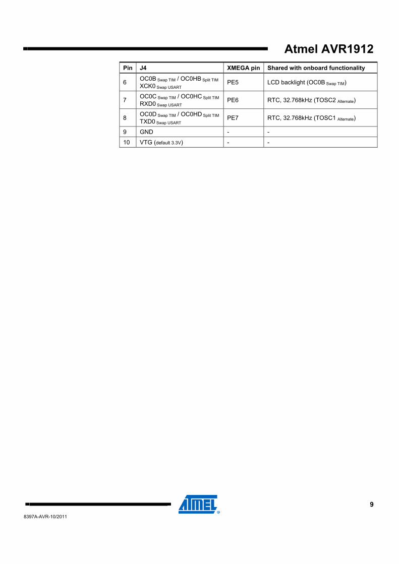
4.3.4 Header – J4
Table 4-6. J4 I/O expansion header. Pin J4 XMEGA pin Shared with onboard functionality
1 OC0A TIM / OC0LA Split TIM PE0 QTOUCH0 (PE0)
2 OC0B TIM / OC0LB Split TIM
XCK0 USART PE1 QTOUCH1 (PE1)
3 OC0C TIM / OC0LC Split TIM
RXD0 USART PE2 QTOUCH2 (PE2)
4 OC0D TIM / OC0LD Split TIM TXD0 USART PE3 QTOUCH3 (PE3)
5 OC0A Swap TIM / OC0HA Split TIM PE4 Power LED (PE4)
Atmel AVR1912
98397A-AVR-10/2011
Pin J4 XMEGA pin Shared with onboard functionality
6 OC0B Swap TIM / OC0HB Split TIM
XCK0 Swap USART PE5 LCD backlight (OC0B Swap TIM)
7 OC0C Swap TIM / OC0HC Split TIM
RXD0 Swap USART PE6 RTC, 32.768kHz (TOSC2 Alternate)
8 OC0D Swap TIM / OC0HD Split TIMTXD0 Swap USART PE7 RTC, 32.768kHz (TOSC1 Alternate)
9 GND - -
10 VTG (default 3.3V) - -
10 Atmel AVR1912 8397A-AVR-10/2011
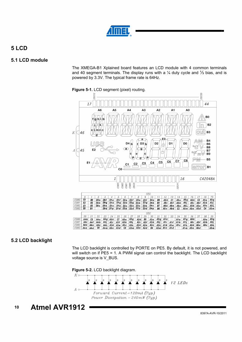
5 LCD
5.1 LCD module The XMEGA-B1 Xplained board features an LCD module with 4 common terminals and 40 segment terminals. The display runs with a ¼ duty cycle and ⅓ bias, and is powered by 3.3V. The typical frame rate is 64Hz.
Figure 5-1. LCD segment (pixel) routing.
5.2 LCD backlight The LCD backlight is controlled by PORTE on PE5. By default, it is not powered, and will switch on if PE5 = 1. A PWM signal can control the backlight. The LCD backlight voltage source is V_BUS.
Figure 5-2. LCD backlight diagram.
Atmel AVR1912
118397A-AVR-10/2011
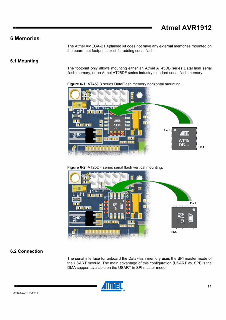
6 Memories The Atmel XMEGA-B1 Xplained kit does not have any external memories mounted on the board, but footprints exist for adding serial flash.
6.1 Mounting The footprint only allows mounting either an Atmel AT45DB series DataFlash serial flash memory, or an Atmel AT25DF series industry standard serial flash memory.
Figure 6-1. AT45DB series DataFlash memory horizontal mounting.
Figure 6-2. AT25DF series serial flash vertical mounting.
6.2 Connection The serial interface for onboard the DataFlash memory uses the SPI master mode of the USART module. The main advantage of this configuration (USART vs. SPI) is the DMA support available on the USART in SPI master mode.
12 Atmel AVR1912 8397A-AVR-10/2011
Table 6-1. Atmel XMEGA-B1 Xplained kit DataFlash connection. DataFlash signal XMEGA signal XMEGA pin Comment
SCK SCK USART-SPI PC5 Shared with J1
SO MISO USART-SPI PC6 Shared with J1
SI MOSI USART-SPI PC7 Shared with J1
/CS (GPIO) PD2 Onboard 100kΩ pull-up resistor
6.3 Compatible devices Table 6-2. Compatible devices for the XMEGA-B1 Xplained kit serial flash footprints.
Atmel AT45DB Series Devices Atmel AT25DF Series Devices
AT45DB64D2-CNU AT25DF641A-SH
AT45DB321D-MWU AT25DF321A-SH
AT45DB161D-SS AT25DF161-SH
AT45DB081D-SS AT25DF081-SSH
AT45DB041D-SS AT25DF021-SSH
AT45DB021D-SS
AT45DB011D-SS
Atmel AVR1912
138397A-AVR-10/2011
7 Miscellaneous I/Os
7.1 Touch The board is equipped with four Atmel QTouch keys. The QTouch functionality is handled by a QTouch device, the Atmel AT42QT1040. Keys are included on the PCB itself (CS[3:0]). By default, the QTouch device is configured in ASK (Adjacent Key Suppression®) mode, and so key combinations are not possible.
An AT42QT1040 output pin goes active low when the corresponding key is touched. Because outputs are of the open-drain type, it is necessary to activate the internal pull-up resistors of PORTE (PE[7:4]) as soon as possible in the application firmware.
NOTE Adding top modules to the board with functionality connected to these pins is not recommended. But, if no key is touched, the module functionality will run correctly.
NOTE The QTouch device is very close to the keys. The sensitivity of the sensor lines on device’s exposed pins is very high, and so touching its I/O pins will give erroneous results for the touch sensing mechanism.
7.2 LEDs
7.2.1 User LEDs
Four yellow LEDs are connected to PORTB on PB[7:4]. The LEDs are active low, and lights up when the respective lines are output low by the Atmel ATxmega128B1.
7.2.2 Power LED
The green LED, mounted near the PDI connector and labeled “POWER,” indicates whether the output voltage generated by the regulator is present. It is connected to PORTE on PE4. This LED is powered by default, and will switch off when PE4 = 0.
7.3 Analog inputs The Atmel XMEGA-B1 Xplained offers two sensors: a temperature sensor and a light sensor. In single-ended mode, it can also measure two analog inputs, one from the on-board potentiometer and one from a source that is external to the board.
7.3.1 Temperature sensor
The temperature sensor employs an NTC thermistor connected to PORTB on pin PB0. The output range of the network containing the NTC is 0V – 1.1V (or 0V – 1/3VTG).
NTC reference: NCP18WF104J03RB.
14 Atmel AVR1912 8397A-AVR-10/2011
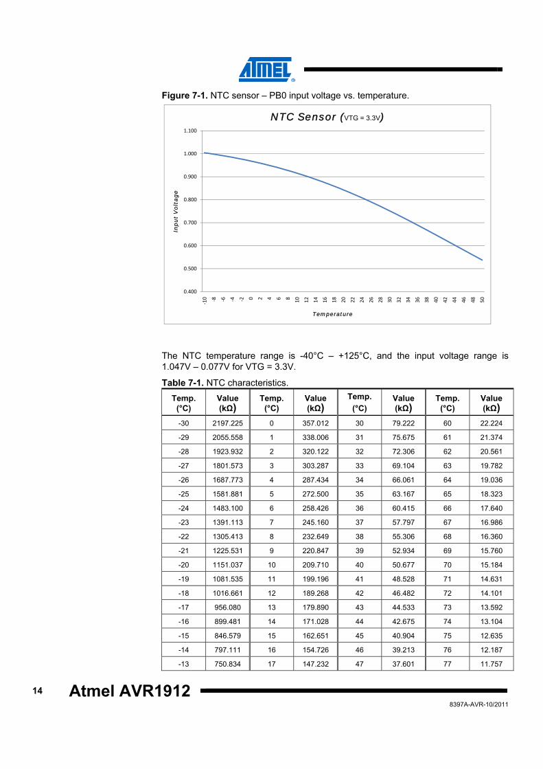
Figure 7-1. NTC sensor – PB0 input voltage vs. temperature.
0.400
0.500
0.600
0.700
0.800
0.900
1.000
1.100
‐10 ‐8 ‐6 ‐4 ‐2 0 2 4 6 8 10 12 14 16 18 20 22 24 26 28 30 32 34 36 38 40 42 44 46 48 50
Inp
ut
Volt
age
Temperature
NTC Sensor (VTG = 3.3V)
The NTC temperature range is -40°C – +125°C, and the input voltage range is 1.047V – 0.077V for VTG = 3.3V.
Table 7-1. NTC characteristics. Temp.
(°C) Value (kΩ)
Temp. (°C)
Value (kΩ)
Temp. (°C)
Value (kΩ)
Temp. (°C)
Value (kΩ)
-30 2197.225 0 357.012 30 79.222 60 22.224
-29 2055.558 1 338.006 31 75.675 61 21.374
-28 1923.932 2 320.122 32 72.306 62 20.561
-27 1801.573 3 303.287 33 69.104 63 19.782
-26 1687.773 4 287.434 34 66.061 64 19.036
-25 1581.881 5 272.500 35 63.167 65 18.323
-24 1483.100 6 258.426 36 60.415 66 17.640
-23 1391.113 7 245.160 37 57.797 67 16.986
-22 1305.413 8 232.649 38 55.306 68 16.360
-21 1225.531 9 220.847 39 52.934 69 15.760
-20 1151.037 10 209.710 40 50.677 70 15.184
-19 1081.535 11 199.196 41 48.528 71 14.631
-18 1016.661 12 189.268 42 46.482 72 14.101
-17 956.080 13 179.890 43 44.533 73 13.592
-16 899.481 14 171.028 44 42.675 74 13.104
-15 846.579 15 162.651 45 40.904 75 12.635
-14 797.111 16 154.726 46 39.213 76 12.187
-13 750.834 17 147.232 47 37.601 77 11.757
Atmel AVR1912
158397A-AVR-10/2011
Temp. (°C)
Value (kΩ)
Temp. (°C)
Value (kΩ)
Temp. (°C)
Value (kΩ)
Temp. (°C)
Value (kΩ)
-12 707.524 18 140.142 48 36.063 78 11.344
-11 666.972 19 133.432 49 34.595 79 10.947
-10 628.988 20 127.080 50 33.195 80 10.566
-9 593.342 21 121.066 51 31.859 81 10.200
-8 559.931 22 115.368 52 30.584 82 9.848
-7 528.602 23 109.970 53 29.366 83 9.510
-6 499.212 24 104.852 54 28.203 84 9.185
-5 471.632 25 100.000 55 27.091 85 8.873
-4 445.772 26 95.398 56 26.028 86 8.572
-3 421.480 27 91.032 57 25.013 87 8.283
-2 398.652 28 86.889 58 24.042 88 8.006
-1 377.193 29 82.956 59 23.113 89 7.738
7.3.2 Light sensor
The light sensor employs a light dependant resistor (LDR) connected to PORTB on pin PB2. The output range of the network containing the LDR is 0V – 1.1V (or 0V – 1/3VTG).
When the light level is low, the resistance of the LDR is high, and the input voltage is close to 1.1V (or 1/3VTG).
7.3.3 Potentiometer voltage
The single-ended output of the onboard potentiometer can be measured at PORTB on pin PB1. The input range is 0V – 0.666V (or 0V – 1/5VTG).
7.3.4 External voltage input
An external voltage can be applied to the kit by using a header, as shown in Figure 3-1. This voltage is routed to pin PB3 on PORTB of the Atmel XMEGA device, and can be determined by a single-ended measurement using the analog-to-digital converter (ADC). However, the external voltage is divided by eight before it is applied to the ADC, and this divider is fixed.
NOTE A 2.0V Zener diode is mounted in parallel with the ADC input. This protects the ADC input from any over voltage. That effectively means that an external voltage between 0V-16V is allowed, assuming VTG is greater than 2.0V.
WARNING If VTG is lower than 2.0V, the ADC input is not protected and the external voltage input must be in the range of 0V – 8*VTG. Otherwise, the device may be damaged.

16 Atmel AVR1912 8397A-AVR-10/2011
8 Further code examples and drivers Several Getting Started training materials for the Atmel XMEGA-B1 Xplained kit can be downloaded from the Atmel website. These training materials offer a general introduction to Atmel ATxmega128B1 peripherals.
Further information and drivers for XMEGA devices can be downloaded as application notes, also distributed from the Atmel website.

Atmel AVR1912
178397A-AVR-10/2011
9 Known issues No known issues.
18 Atmel AVR1912 8397A-AVR-10/2011
10 Revision history The revision of the evaluation kit can be found on the bottom of the PCB.
Revision 4 of the Atmel XMEGA-B1 Xplained kit can be identified by a barcode sticker on the back side of the PCB with the following product ID: A09-1060/6.
10.1 Revision 6 Revision 6 is the first released version of the XMEGA-B1 Xplained kit, and it employs revision 3 of the PCB (product ID: A08-0840/3).
10.2 Revision 1 up to 5 Not released.
Atmel AVR1912
198397A-AVR-10/2011
11 Evaluation board/kit important notice This evaluation board/kit is intended for use for FURTHER ENGINEERING, DEVELOPMENT, DEMONSTRATION, OR EVALUATION PURPOSES ONLY. It is not a finished product, and may not (yet) comply with some or any technical or legal requirements that are applicable to finished products, including, without limitation, directives regarding electromagnetic compatibility, recycling (WEEE), FCC, CE, or UL (except as may be otherwise noted on the board/kit). Atmel supplied this board/kit “AS IS,” without any warranties, with all faults, at the buyer’s and further users’ sole risk. The user assumes all responsibility and liability for proper and safe handling of the goods. Further, the user indemnifies Atmel from all claims arising from the handling or use of the goods. Due to the open construction of the product, it is the user’s responsibility to take any and all appropriate precautions with regard to electrostatic discharge and any other technical or legal concerns.
EXCEPT TO THE EXTENT OF THE INDEMNITY SET FORTH ABOVE, NEITHER USER NOR ATMEL SHALL BE LIABLE TO EACH OTHER FOR ANY INDIRECT, SPECIAL, INCIDENTAL, OR CONSEQUENTIAL DAMAGES.
No license is granted under any patent right or other intellectual property right of Atmel covering or relating to any machine, process, or combination in which such Atmel products or services might be or are used.
Mailing Address: Atmel Corporation, 2325 Orchard Parkway, San Jose, CA 95131.
20 Atmel AVR1912 8397A-AVR-10/2011
12 Table of contents Features............................................................................................... 1 1 Introduction ...................................................................................... 1 2 Related items.................................................................................... 2 3 General information......................................................................... 3
3.1 Preprogrammed firmware.................................................................................... 4 3.2 Power supply ....................................................................................................... 4 3.3 Measuring Atmel ATxmega128B1 power consumption ...................................... 5 3.4 Programming the ATxmega128B1 through the USB interface ........................... 5
4 Connectors ....................................................................................... 6 4.1 Programming and debugging header.................................................................. 6 4.2 USB connector .................................................................................................... 7 4.3 Expansion headers.............................................................................................. 7
4.3.1 Header – J1............................................................................................................... 7 4.3.2 Header – J2............................................................................................................... 8 4.3.3 Header – J3............................................................................................................... 8 4.3.4 Header – J4............................................................................................................... 8
5 LCD ................................................................................................. 10 5.1 LCD module....................................................................................................... 10 5.2 LCD backlight .................................................................................................... 10
6 Memories ........................................................................................ 11 6.1 Mounting............................................................................................................ 11 6.2 Connection ........................................................................................................ 11 6.3 Compatible devices ........................................................................................... 12
7 Miscellaneous I/Os......................................................................... 13 7.1 Touch................................................................................................................. 13 7.2 LEDs.................................................................................................................. 13
7.2.1 User LEDs ............................................................................................................... 13 7.2.2 Power LED .............................................................................................................. 13
7.3 Analog inputs..................................................................................................... 13 7.3.1 Temperature sensor ................................................................................................ 13 7.3.2 Light sensor............................................................................................................. 15 7.3.3 Potentiometer voltage.............................................................................................. 15 7.3.4 External voltage input .............................................................................................. 15
8 Further code examples and drivers ............................................. 16 9 Known issues................................................................................. 17 10 Revision history ........................................................................... 18
10.1 Revision 6........................................................................................................ 18
Atmel AVR1912
218397A-AVR-10/2011
10.2 Revision 1 up to 5............................................................................................ 18 11 Evaluation board/kit important notice........................................ 19 12 Table of contents ......................................................................... 20

8397A-AVR-10/2011
Atmel Corporation 2325 Orchard Parkway San Jose, CA 95131 USA Tel: (+1)(408) 441-0311 Fax: (+1)(408) 487-2600 www.atmel.com
Atmel Asia Limited Unit 01-5 & 16, 19F BEA Tower, Milennium City 5 418 Kwun Tong Road Kwun Tong, Kowloon HONG KONG Tel: (+852) 2245-6100 Fax: (+852) 2722-1369
Atmel Munich GmbH Business Campus Parkring 4 D-85748 Garching b. Munich GERMANY Tel: (+49) 89-31970-0 Fax: (+49) 89-3194621
Atmel Japan 9F, Tonetsu Shinkawa Bldg. 1-24-8 Shinkawa Chou-ku, Tokyo 104-0033 JAPAN Tel: (+81) 3523-3551 Fax: (+81) 3523-7581
© 2011 Atmel Corporation. All rights reserved.
Atmel®, Atmel logo and combinations thereof, AVR®, AVR Studio®, Adjacent Key Suppression®, DataFlash®, QTouch®, XMEGA®, and others are registered trademarks or trademarks of Atmel Corporation or its subsidiaries. Other terms and product names may be trademarks of others. Disclaimer: The information in this document is provided in connection with Atmel products. No license, express or implied, by estoppel or otherwise, to any intellectual property right is granted by this document or in connection with the sale of Atmel products. EXCEPT AS SET FORTH IN THE ATMEL TERMS AND CONDITIONS OF SALES LOCATED ON THE ATMEL WEBSITE, ATMEL ASSUMES NO LIABILITY WHATSOEVER AND DISCLAIMS ANY EXPRESS, IMPLIED OR STATUTORY WARRANTY RELATING TO ITS PRODUCTS INCLUDING, BUT NOT LIMITED TO, THE IMPLIED WARRANTY OF MERCHANTABILITY, FITNESS FOR A PARTICULAR PURPOSE, OR NON-INFRINGEMENT. IN NO EVENT SHALL ATMEL BE LIABLE FOR ANY DIRECT, INDIRECT, CONSEQUENTIAL, PUNITIVE, SPECIAL OR INCIDENTAL DAMAGES (INCLUDING, WITHOUT LIMITATION, DAMAGES FOR LOSS AND PROFITS, BUSINESS INTERRUPTION, OR LOSS OF INFORMATION) ARISING OUT OF THE USE OR INABILITY TO USE THIS DOCUMENT, EVEN IF ATMEL HAS BEEN ADVISED OF THE POSSIBILITY OF SUCH DAMAGES. Atmel makes no representations or warranties with respect to the accuracy or completeness of the contents of this document and reserves the right to make changes to specifications and product descriptions at any time without notice. Atmel does not make any commitment to update the information contained herein. Unless specifically provided otherwise, Atmel products are not suitable for, and shall not be used in, automotive applications. Atmel products are not intended, authorized, or warranted for use as components in applications intended to support or sustain life.
![Atmel SAM R21 Xplained Pro (USER GUIDE) - Mouser Electronics · Atmel SAM R21 Xplained Pro [USER GUIDE] 42243A-MCU-02/2014 6 3. Xplained Pro Xplained Pro is an evaluation platform](https://img.pdfslide.net/doc/110x75/5c7395a209d3f2123b8b83c4/atmel-sam-r21-xplained-pro-user-guide-mouser-atmel-sam-r21-xplained-pro.jpg)
![Atmel AT01639: XMEGA-C3 Xplained Software …ww1.microchip.com/downloads/en/AppNotes/Atmel-42090...Atmel AT01639: XMEGA-C3 Xplained Software User Guide [APPLICATION NOTE] 42090A−AVR−02/2013](https://img.pdfslide.net/doc/110x75/5ee0c5daad6a402d666be2b6/atmel-at01639-xmega-c3-xplained-software-ww1-atmel-at01639-xmega-c3-xplained.jpg)

![Atmel AVR XMEGA D Manual - Microchip Technologyww1.microchip.com/downloads/en/DeviceDoc/Atmel-8210-8... · 2017-05-05 · XMEGA D [MANUAL] 5 Atmel-8210G–AVR XMEGA D–12/2014 Table](https://img.pdfslide.net/doc/110x75/5ed43e2c1e109569e1214450/atmel-avr-xmega-d-manual-microchip-2017-05-05-xmega-d-manual-5-atmel-8210gaavr.jpg)


![Atmel AVR XMEGA B Manual - Microchip Technologyww1.microchip.com/...8-and-16-bit-AVR-Microcontrollers-XMEGA-B_M… · XMEGA B MANUAL. XMEGA B [MANUAL] 2 Atmel-8291C-AVR-XMEGA B -09/2014](https://img.pdfslide.net/doc/110x75/5b76f9aa7f8b9ade6f8c05a8/atmel-avr-xmega-b-manual-microchip-xmega-b-manual-xmega-b-manual-2-atmel-8291c-avr-xmega.jpg)


![Atmel AT02657: XMEGA-E5 Xplained Software User Guideww1.microchip.com/downloads/en/AppNotes/Atmel... · Atmel AT02657: XMEGA-E5 Xplained Software User Guide [APPLICATION NOTE] 42085A−AVR−04/2013](https://img.pdfslide.net/doc/110x75/5f88ba81f6b36722b04d705d/atmel-at02657-xmega-e5-xplained-software-user-atmel-at02657-xmega-e5-xplained.jpg)


![Atmel | SMART SAMA5D3 Series - Microchip Technologyww1.microchip.com/downloads/en/DeviceDoc/Atmel-11269-32...SAMA5D3 Xplained [USER GUIDE] Atmel-11269D-ATARM-SAMA5D3-Xplained-XPLD-User](https://img.pdfslide.net/doc/110x75/5aedd4107f8b9a3669917d67/atmel-smart-sama5d3-series-microchip-xplained-user-guide-atmel-11269d-atarm-sama5d3-xplained-xpld-user.jpg)