Embed Size (px)
Citation preview
Atomic and Electronic Structures of WTe2 Probed by High ResolutionElectron Microscopy and ab Initio CalculationsNing Lu,† Chenxi Zhang,† Chia-Hui Lee,‡,∥ Juan Pablo Oviedo,† Minh An T. Nguyen,§,∥ Xin Peng,†
Robert M. Wallace,† Thomas E. Mallouk,§,∥ Joshua A. Robinson,‡,∥ Jinguo Wang,† Kyeongjae Cho,†
and Moon J. Kim*,†
†Department of Materials Science and Engineering, The University of Texas at Dallas, Richardson, Texas 75080, United States‡Department of Materials Science and Engineering, §Department of Chemistry, and ∥Center for 2-Dimensional and LayeredMaterials, The Pennsylvania State University, University Park, Pennsylvania 16802, United States
*S Supporting Information
ABSTRACT: Transition metal dichalcogenides (TMDs) are a class oftwo-dimensional (2D) materials that have attracted growing interestbecause of their unique electronic and optical properties. Under ambientconditions, most TMDs generally exhibit 2H or 1T structures. Unlikeother group VIb TMDs, bulk crystals and powders of WTe2 exist in adistorted 1T structure (Td) at room temperature and have semimetallicproperties. There is so far a lack of direct atom-by-atom visualization,limiting our understanding of this distorted 2D layered material system.We present herein atomic resolution images of Td structured WTe2. TheTd structure can be distinguished in the three major orientations alongthe [100], [010], and [001] zone axes. Subtle structural distortions aredetected by atomic resolution imaging, which match well with theoptimized structure relaxed by ab initio calculations. The calculations also showed that both crystal field splitting and chargedensity wave (CDW) interactions contribute to the stabilization of WTe2. However, the CDW interaction dominates and leadsthe Td-WTe2 to be the most stable structure. The combined atomic resolution STEM and ab initio study on WTe2 provided thebasis for understanding the correlations between atomic structure and electronic properties in Td structured TMD materials.
■ INTRODUCTION
Transition metal dichalcogenides (TMDs) MX2, where M is atransition metal (Mo, W, Hf, etc.) and X is a chalcogen (S, Se,and Te), are a class of two-dimensional (2D) materials thathave attracted growing interest because of their uniqueelectronic and optical properties.1−3 Recent reports haveexplored the crystal structures, syntheses, and electronicproperties of TMD systems using both experimental andtheoretical techniques.4 These studies suggest that the absenceof dangling bonds5 and the wide range of band gaps (from 3.5to <1 eV)6 make TMD materials attractive in practical devices,such as field effect transistors2,7,8 and photosensors.9,10
TMDs have layered structures with an X−M−X atomicstacking sequence in each layer. When the M atoms arecoordinated by a trigonal prism of X atoms, the structure isdefined as the 2H phase,11 as shown in Figure 1a. There aretwo X−M−X layers in each unit cell of the 2H structure. GroupVIb TMDs that adopt the 2H structure, such as MoS2 and WS2,are usually semiconductors with band gaps between 1 and 2eV.1,6 When one X layer is shifted such that the metal becomesoctahedrally coordinated, the structure is referred to as the 1Tphase,11 as shown in Figure 1b. In this case there is only oneX−M−X layer in the unit cell. The 1T structure TMDs cover abroad spectrum of electrical properties, from insulators such as
HfS2, through semiconductors such as HfSe2, to metals such asTiS2.
11 Under ambient conditions, most TMDs exist in 2H or1T structures. Unlike other group VIb TMDs, bulk crystals andpowders of WTe2 are generally found in a distorted 1Tstructure (Td, also called 1T′) at room temperature and havesemimetallic properties.12−18 Reports of the 2H (semiconduct-ing) phase of WTe2 appear to be limited to the powdersynthesis work by Champion19 and have been summarized inthe review by Wilson and Yoffe.11 Ab initio calculations havebeen used to investigate the electronic structure of WTe2, and ithas been found they exhibit semimetal properties which arisefrom the small electron and hole pockets along the Γ−Xdirection.15,20 Another possible explanation is that there is a 0.5eV overlap of Te 5p and W 5d-like bands along Γ−Y, and thelow conductivity of WTe2 is due to the low density of states atthe Fermi level.21 Angle-resolved photoemission spectroscopy(ARPES) was used to confirm the electronic structure of WTe2,and it was found that carrier compensation would be theprimary source of formation of similar-sized electron and holepockets.22 Very recently, an extremely large positive magneto-
Received: January 30, 2016Revised: April 3, 2016Published: April 5, 2016
Article
pubs.acs.org/JPCC
© 2016 American Chemical Society 8364 DOI: 10.1021/acs.jpcc.6b01044J. Phys. Chem. C 2016, 120, 8364−8369
resistance at low temperatures has been discovered in thenonmagnetic Td structure WTe2.
20 Although electrical andmagnetic studies of WTe2 as a novel material system have beencarried out, there is so far a lack of direct atom-by-atomvisualization, limiting our understanding of this distorted 2Dlayered material system. Moreover, the correlation between thestructure and electronic properties in WTe2 also has not beenwell understood yet. Here we have combined atomic imagingand ab initio calculations to reveal the atomic and electronicstructures of Td-WTe2. Furthermore, charge density wave(CDW) is used to understand the atomic structure andelectronic property correlations in WTe2.
■ EXPERIMENTAL METHODSSynthesis of WTe2 Flakes. WTe2 bulk crystals were
produced by the chemical vapor transport method usingbromine as the transport agent. The details of the syntheticmethod can be found in the previous work.18 The X-raydiffraction (XRD) patterns of the synthesized WTe2 flakesconfirmed the bulk WTe2 crystals are orthorhombic spacegroup Pmn21, with Td structure.18
Atomic Imaging and Image Simulations. Transmissionelectron microscopic (TEM) cross-sectional samples weremade by using a FEI Nova 200 dual-beam focused ion beamscanning electron microscope (FIB/SEM) by the lift-outmethod. In the FIB, SiO2 and Pt layers were deposited toprotect the region of interest during focused ion beam milling.Atomic high angle angular dark field scanning transmissionelectron microscopy (HAADF-STEM) was performed in aJEOL ARM200F microscope with a probe aberration corrector(CEOS GmbH) operated at 200 kV. HAADF-STEM imagesbased on the optimized atomic structure were simulated usingthe xHREM software package.Ab Initio Calculations. The calculations were performed
by using the Vienna Ab initio Simulation Package (VASP).23
The projector-augmented wave (PAW) pseudopotential24 isadopted, and the generalized gradient approximation (GGA) ofPerdew−Burke−Ernzerhof (PBE) functionals were used todescribe the exchange−correlation.25 Spin−orbit coupling isincluded for the band structure calculations along highsymmetry points in the Brillouin zone (BZ).
In this work, the structures of all the TMDs studied wereoptimized based on both 2H and 1T bulk crystal structures,with the remnant force on each atom below 0.01 eV/Å as thestopping criterion for ionic relaxation. The Grimme-D3correction, to correct the van der Waals (vdW) interactionbetween layers, is included in order to get a better optimizedcrystal structure of bulk WTe2.
26,27 The Monkhorst−Pack k-point sampling in BZ is Γ-centered with 6 × 12 × 4 and 24 ×24 × 8 meshes in ionic and electronic optimization,respectively.28 The energy cutoff is 500 eV. The electronicoptimization was stopped when the total energies ofneighboring loops differed by less than 10−4 eV.
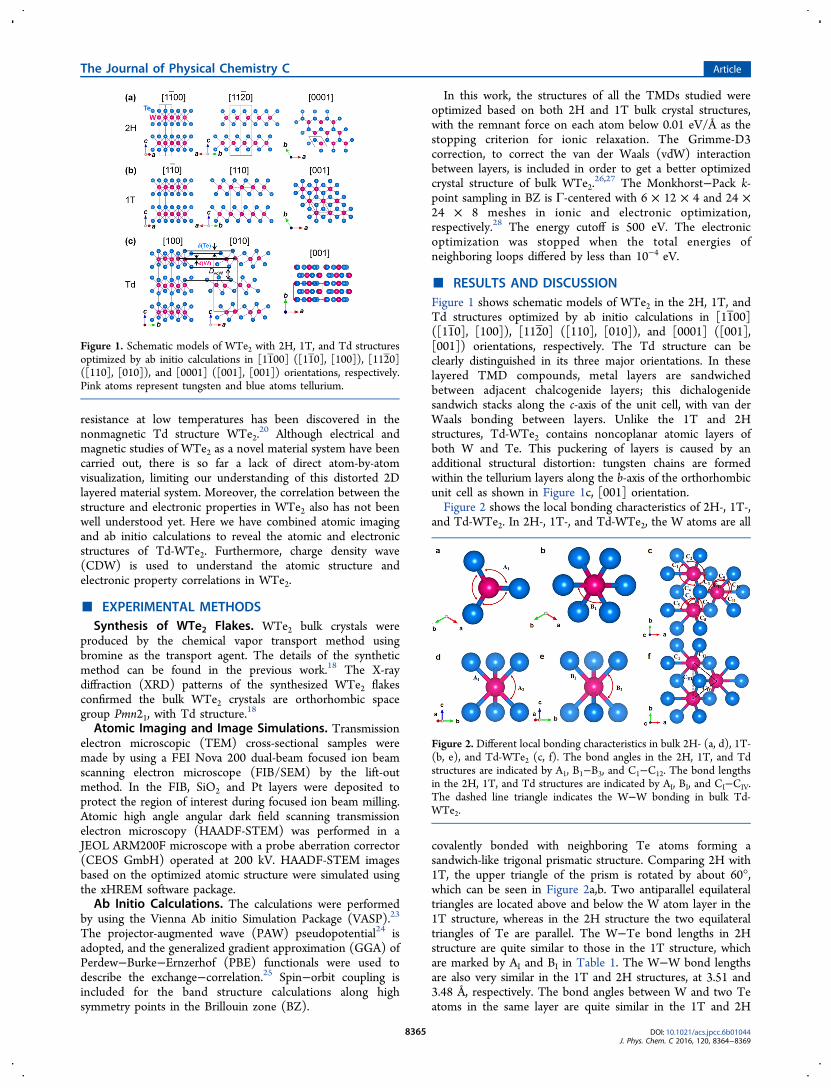
■ RESULTS AND DISCUSSIONFigure 1 shows schematic models of WTe2 in the 2H, 1T, andTd structures optimized by ab initio calculations in [11̅00]([11 ̅0], [100]), [112 ̅0] ([110], [010]), and [0001] ([001],[001]) orientations, respectively. The Td structure can beclearly distinguished in its three major orientations. In theselayered TMD compounds, metal layers are sandwichedbetween adjacent chalcogenide layers; this dichalogenidesandwich stacks along the c-axis of the unit cell, with van derWaals bonding between layers. Unlike the 1T and 2Hstructures, Td-WTe2 contains noncoplanar atomic layers ofboth W and Te. This puckering of layers is caused by anadditional structural distortion: tungsten chains are formedwithin the tellurium layers along the b-axis of the orthorhombicunit cell as shown in Figure 1c, [001] orientation.Figure 2 shows the local bonding characteristics of 2H-, 1T-,
and Td-WTe2. In 2H-, 1T-, and Td-WTe2, the W atoms are all
covalently bonded with neighboring Te atoms forming asandwich-like trigonal prismatic structure. Comparing 2H with1T, the upper triangle of the prism is rotated by about 60°,which can be seen in Figure 2a,b. Two antiparallel equilateraltriangles are located above and below the W atom layer in the1T structure, whereas in the 2H structure the two equilateraltriangles of Te are parallel. The W−Te bond lengths in 2Hstructure are quite similar to those in the 1T structure, whichare marked by AI and BI in Table 1. The W−W bond lengthsare also very similar in the 1T and 2H structures, at 3.51 and3.48 Å, respectively. The bond angles between W and two Teatoms in the same layer are quite similar in the 1T and 2H
Figure 1. Schematic models of WTe2 with 2H, 1T, and Td structuresoptimized by ab initio calculations in [11̅00] ([11 ̅0], [100]), [112̅0]([110], [010]), and [0001] ([001], [001]) orientations, respectively.Pink atoms represent tungsten and blue atoms tellurium.
Figure 2. Different local bonding characteristics in bulk 2H- (a, d), 1T-(b, e), and Td-WTe2 (c, f). The bond angles in the 2H, 1T, and Tdstructures are indicated by A1, B1−B3, and C1−C12. The bond lengthsin the 2H, 1T, and Td structures are indicated by AI, BI, and CI−CIV.The dashed line triangle indicates the W−W bonding in bulk Td-WTe2.
The Journal of Physical Chemistry C Article
DOI: 10.1021/acs.jpcc.6b01044J. Phys. Chem. C 2016, 120, 8364−8369
8365
structures (A1 80.25° and B1 78.80°). In contrast, the bondangles between W and Te atoms in different layers are differentin the 2H and 1T structures because of the rotation of Tetriangles in the 1T structure (A2 is 83.82° and B2 is 101.20°). Inthe Td structure, the W atoms are shifted from the center of theprisms forming a zigzag chain along the b-axis which can beseen in Figure 2f (black triangle). One pair of W−W bondsbecomes shorter while the other becomes longer because of theexistence of charge density wave distortion.29 The W−W bondlength is much shorter than that in the 2H and 1T structures, asshown in Table 1. The length of one W−W bond (CII in Table1, 2.71 Å) is close to that in tungsten metal (2.74 Å). Due tothe shift of W atoms, the bond lengths and bond angles of Td-WTe2 are modified compared to the 1T structure. Three W−Te bonds are shortened (CII), and the other three are stretched(CI). The Te plane is crumpled due to the distortion andforming a zigzag shape, as shown in Figure 1c. Because of thedisplacement of W atoms from the center, the originaloctahedral symmetry is broken and the octahedron formedby W and its six neighboring Te’s are distorted causing therandom distribution of bond angles between W and Te atoms(shown in Table 1).The vertical shift along the c-axis of W and Te atoms is an
obvious feature in the [100] and [010] views of the structure, asshown in Figure 1c. These atoms form zigzag-like planes,especially the Te layers which form a buckled van der Waalsgap. We define the vertical displacement between the nearestneighbor W and Te atoms as δ(W) and δ(Te), as indicated inFigure 1c. The size of the buckled van der Waals gap (DvdW, inFigure 1c) is expressed as the closest tellurium−telluriumvertical distance. Dc denotes the lattice parameter of the unitcell along the c-axis. We can obtain the relative verticaldisplacement of nearest neighbor W and Te atoms in the Tdunit cell by using Δ(W) = δ(W)/Dc and Δ(Te) = δ(Te)/Dc. Inthe relaxed Td structure, Dc = 14.06 Å, DvdW ∼ 3.47 Å, δ(W) ∼0.21 Å, Δ(W) ∼ 1.5%, δ(Te) ∼ 0.63 Å, and Δ(Te) ∼ 4.5%.These subtle structural distortions can be detected by atomichigh angle angular dark field (HAADF) scanning transmissionelectron microscopy (STEM) imaging as shown below.Figure 3 shows experimental HAADF-STEM atomic images
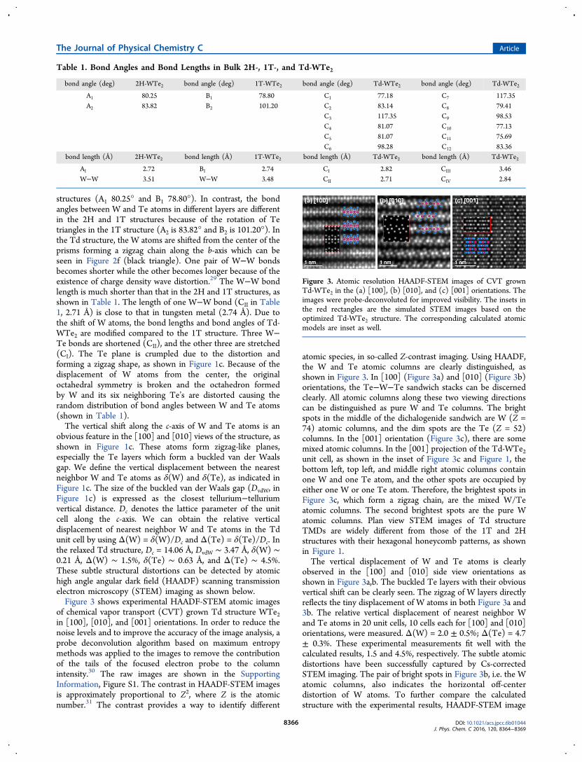
of chemical vapor transport (CVT) grown Td structure WTe2in [100], [010], and [001] orientations. In order to reduce thenoise levels and to improve the accuracy of the image analysis, aprobe deconvolution algorithm based on maximum entropymethods was applied to the images to remove the contributionof the tails of the focused electron probe to the columnintensity.30 The raw images are shown in the SupportingInformation, Figure S1. The contrast in HAADF-STEM imagesis approximately proportional to Z2, where Z is the atomicnumber.31 The contrast provides a way to identify different
atomic species, in so-called Z-contrast imaging. Using HAADF,the W and Te atomic columns are clearly distinguished, asshown in Figure 3. In [100] (Figure 3a) and [010] (Figure 3b)orientations, the Te−W−Te sandwich stacks can be discernedclearly. All atomic columns along these two viewing directionscan be distinguished as pure W and Te columns. The brightspots in the middle of the dichalogenide sandwich are W (Z =74) atomic columns, and the dim spots are the Te (Z = 52)columns. In the [001] orientation (Figure 3c), there are somemixed atomic columns. In the [001] projection of the Td-WTe2unit cell, as shown in the inset of Figure 3c and Figure 1, thebottom left, top left, and middle right atomic columns containone W and one Te atom, and the other spots are occupied byeither one W or one Te atom. Therefore, the brightest spots inFigure 3c, which form a zigzag chain, are the mixed W/Teatomic columns. The second brightest spots are the pure Watomic columns. Plan view STEM images of Td structureTMDs are widely different from those of the 1T and 2Hstructures with their hexagonal honeycomb patterns, as shownin Figure 1.The vertical displacement of W and Te atoms is clearly
observed in the [100] and [010] side view orientations asshown in Figure 3a,b. The buckled Te layers with their obviousvertical shift can be clearly seen. The zigzag of W layers directlyreflects the tiny displacement of W atoms in both Figure 3a and3b. The relative vertical displacement of nearest neighbor Wand Te atoms in 20 unit cells, 10 cells each for [100] and [010]orientations, were measured. Δ(W) = 2.0 ± 0.5%; Δ(Te) = 4.7± 0.3%. These experimental measurements fit well with thecalculated results, 1.5 and 4.5%, respectively. The subtle atomicdistortions have been successfully captured by Cs-correctedSTEM imaging. The pair of bright spots in Figure 3b, i.e. the Watomic columns, also indicates the horizontal off-centerdistortion of W atoms. To further compare the calculatedstructure with the experimental results, HAADF-STEM image
Table 1. Bond Angles and Bond Lengths in Bulk 2H-, 1T-, and Td-WTe2
bond angle (deg) 2H-WTe2 bond angle (deg) 1T-WTe2 bond angle (deg) Td-WTe2 bond angle (deg) Td-WTe2
A1 80.25 B1 78.80 C1 77.18 C7 117.35A2 83.82 B2 101.20 C2 83.14 C8 79.41
C3 117.35 C9 98.53C4 81.07 C10 77.13C5 81.07 C11 75.69C6 98.28 C12 83.36
bond length (Å) 2H-WTe2 bond length (Å) 1T-WTe2 bond length (Å) Td-WTe2 bond length (Å) Td-WTe2
AI 2.72 BI 2.74 CI 2.82 CIII 3.46W−W 3.51 W−W 3.48 CII 2.71 CIV 2.84
Figure 3. Atomic resolution HAADF-STEM images of CVT grownTd-WTe2 in the (a) [100], (b) [010], and (c) [001] orientations. Theimages were probe-deconvoluted for improved visibility. The insets inthe red rectangles are the simulated STEM images based on theoptimized Td-WTe2 structure. The corresponding calculated atomicmodels are inset as well.
The Journal of Physical Chemistry C Article
DOI: 10.1021/acs.jpcc.6b01044J. Phys. Chem. C 2016, 120, 8364−8369
8366
simulations were carried out. HAADF-STEM images based onthe optimized Td atomic structure were simulated along the[100], [010], and [001] zone axes, as shown in the insets withred borders in Figure 3, respectively. The simulated images fitwell with experimental images, confirming the reliability of thecalculated structure of Td-WTe2, which also demonstrates thatthe Grimme-D3 correction of vdW interaction works well insuch distorted layered TMD materials.The good consistency between simulated image based on
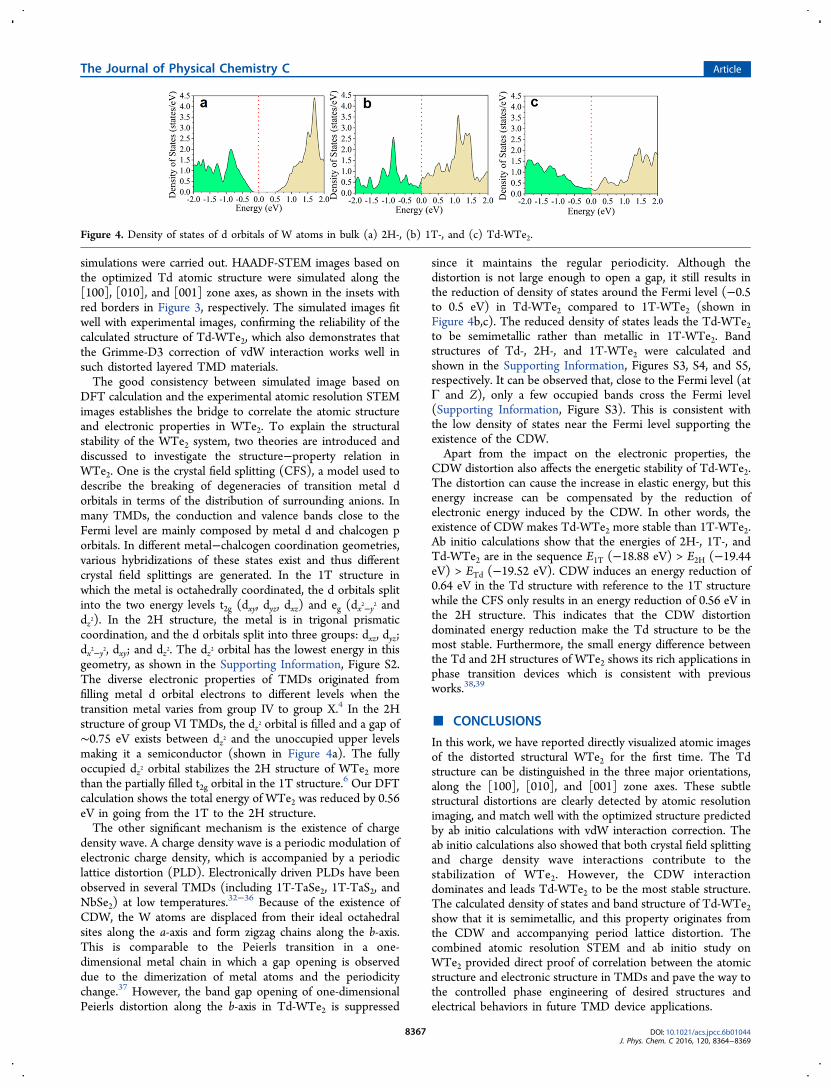
DFT calculation and the experimental atomic resolution STEMimages establishes the bridge to correlate the atomic structureand electronic properties in WTe2. To explain the structuralstability of the WTe2 system, two theories are introduced anddiscussed to investigate the structure−property relation inWTe2. One is the crystal field splitting (CFS), a model used todescribe the breaking of degeneracies of transition metal dorbitals in terms of the distribution of surrounding anions. Inmany TMDs, the conduction and valence bands close to theFermi level are mainly composed by metal d and chalcogen porbitals. In different metal−chalcogen coordination geometries,various hybridizations of these states exist and thus differentcrystal field splittings are generated. In the 1T structure inwhich the metal is octahedrally coordinated, the d orbitals splitinto the two energy levels t2g (dxy, dyz, dxz) and eg (dx2−y2 anddz2). In the 2H structure, the metal is in trigonal prismaticcoordination, and the d orbitals split into three groups: dxz, dyz;dx2−y2, dxy; and dz2. The dz2 orbital has the lowest energy in thisgeometry, as shown in the Supporting Information, Figure S2.The diverse electronic properties of TMDs originated fromfilling metal d orbital electrons to different levels when thetransition metal varies from group IV to group X.4 In the 2Hstructure of group VI TMDs, the dz2 orbital is filled and a gap of∼0.75 eV exists between dz2 and the unoccupied upper levelsmaking it a semiconductor (shown in Figure 4a). The fullyoccupied dz2 orbital stabilizes the 2H structure of WTe2 morethan the partially filled t2g orbital in the 1T structure.6 Our DFTcalculation shows the total energy of WTe2 was reduced by 0.56eV in going from the 1T to the 2H structure.The other significant mechanism is the existence of charge
density wave. A charge density wave is a periodic modulation ofelectronic charge density, which is accompanied by a periodiclattice distortion (PLD). Electronically driven PLDs have beenobserved in several TMDs (including 1T-TaSe2, 1T-TaS2, andNbSe2) at low temperatures.32−36 Because of the existence ofCDW, the W atoms are displaced from their ideal octahedralsites along the a-axis and form zigzag chains along the b-axis.This is comparable to the Peierls transition in a one-dimensional metal chain in which a gap opening is observeddue to the dimerization of metal atoms and the periodicitychange.37 However, the band gap opening of one-dimensionalPeierls distortion along the b-axis in Td-WTe2 is suppressed
since it maintains the regular periodicity. Although thedistortion is not large enough to open a gap, it still results inthe reduction of density of states around the Fermi level (−0.5to 0.5 eV) in Td-WTe2 compared to 1T-WTe2 (shown inFigure 4b,c). The reduced density of states leads the Td-WTe2to be semimetallic rather than metallic in 1T-WTe2. Bandstructures of Td-, 2H-, and 1T-WTe2 were calculated andshown in the Supporting Information, Figures S3, S4, and S5,respectively. It can be observed that, close to the Fermi level (atΓ and Z), only a few occupied bands cross the Fermi level(Supporting Information, Figure S3). This is consistent withthe low density of states near the Fermi level supporting theexistence of the CDW.Apart from the impact on the electronic properties, the
CDW distortion also affects the energetic stability of Td-WTe2.The distortion can cause the increase in elastic energy, but thisenergy increase can be compensated by the reduction ofelectronic energy induced by the CDW. In other words, theexistence of CDW makes Td-WTe2 more stable than 1T-WTe2.Ab initio calculations show that the energies of 2H-, 1T-, andTd-WTe2 are in the sequence E1T (−18.88 eV) > E2H (−19.44eV) > ETd (−19.52 eV). CDW induces an energy reduction of0.64 eV in the Td structure with reference to the 1T structurewhile the CFS only results in an energy reduction of 0.56 eV inthe 2H structure. This indicates that the CDW distortiondominated energy reduction make the Td structure to be themost stable. Furthermore, the small energy difference betweenthe Td and 2H structures of WTe2 shows its rich applications inphase transition devices which is consistent with previousworks.38,39
■ CONCLUSIONS
In this work, we have reported directly visualized atomic imagesof the distorted structural WTe2 for the first time. The Tdstructure can be distinguished in the three major orientations,along the [100], [010], and [001] zone axes. These subtlestructural distortions are clearly detected by atomic resolutionimaging, and match well with the optimized structure predictedby ab initio calculations with vdW interaction correction. Theab initio calculations also showed that both crystal field splittingand charge density wave interactions contribute to thestabilization of WTe2. However, the CDW interactiondominates and leads Td-WTe2 to be the most stable structure.The calculated density of states and band structure of Td-WTe2show that it is semimetallic, and this property originates fromthe CDW and accompanying period lattice distortion. Thecombined atomic resolution STEM and ab initio study onWTe2 provided direct proof of correlation between the atomicstructure and electronic structure in TMDs and pave the way tothe controlled phase engineering of desired structures andelectrical behaviors in future TMD device applications.
Figure 4. Density of states of d orbitals of W atoms in bulk (a) 2H-, (b) 1T-, and (c) Td-WTe2.
The Journal of Physical Chemistry C Article
DOI: 10.1021/acs.jpcc.6b01044J. Phys. Chem. C 2016, 120, 8364−8369
8367
■ ASSOCIATED CONTENT
*S Supporting InformationThe Supporting Information is available free of charge on theACS Publications website at DOI: 10.1021/acs.jpcc.6b01044.
Figures S1−S5 including raw HAADF-STEM images;energy level splitting of d orbitals of W; band structuresof Td-, 2H-, and 1T-WSe2 (PDF)
■ AUTHOR INFORMATION
Corresponding Author*Tel.: 972-883-6635. Fax: 972-883-5725. E-mail: [email protected].
Present AddressN.L.: Micron Technology, Inc., Boise, Idaho 83716, UnitedStates.
Author ContributionsThe manuscript was written through contributions of allauthors. All authors have given approval to the final version ofthe manuscript. N.L. and C.Z. contributed equally.
NotesThe authors declare no competing financial interest.
■ ACKNOWLEDGMENTS
This work was supported by the Center for Low EnergySystems Technology (LEAST), one of six centers supported bythe STARnet phase of the Focus Center Research Program(FCRP), a Semiconductor Research Corporation programsponsored by MARCO and DARPA, and by the LouisBeecherl, Jr., endowment funds. M.A.T.N. and T.E.M.acknowledge support from U.S. Army Research Office MURIGrant W911NF-11-1-0362.
■ REFERENCES(1) Wang, Q. H.; Kalantar-Zadeh, K.; Kis, A.; Coleman, J. N.; Strano,M. S. Electronics and Optoelectronics of Two-Dimensional TransitionMetal Dichalcogenides. Nat. Nanotechnol. 2012, 7, 699−712.(2) Radisavljevic, B.; Radenovic, A.; Brivio, J.; Giacometti, V.; Kis, A.Single-Layer MoS2 Transistors. Nat. Nanotechnol. 2011, 6, 147−150.(3) Levi, R.; Bitton, O.; Leitus, G.; Tenne, R.; Joselevich, E. Field-Effect Transistors Based on WS2 Nanotubes with High Current-Carrying Capacity. Nano Lett. 2013, 13, 3736−3741.(4) Chhowalla, M.; Shin, H. S.; Eda, G.; Li, L. J.; Loh, K. P.; Zhang,H. The Chemistry of Two-Dimensional Layered Transition MetalDichalcogenide Nanosheets. Nat. Chem. 2013, 5, 263−275.(5) Jena, D. Tunneling Transistors Based on Graphene and 2-DCrystals. Proc. IEEE 2013, 101, 1585−1602.(6) Gong, C.; Zhang, H. J.; Wang, W. H.; Colombo, L.; Wallace, R.M.; Cho, K. J. Band Alignment of Two-Dimensional Transition MetalDichalcogenides: Application in Tunnel Field Effect Transistors. Appl.Phys. Lett. 2013, 103, 053513.(7) Lam, K. T.; Cao, X.; Guo, J. Device Performance ofHeterojunction Tunneling Field-Effect Transistors Based on Tran-sition Netal Dichalcogenide Monolayer. IEEE Electron Device Lett.2013, 34, 1331−1333.(8) Ilatikhameneh, H.; Tan, Y.; Novakovic, B.; Klimeck, G.; Rahman,R.; Appenzeller, J. Tunnel Field-Effect Transistors in 2D TransitionMetal Dichalcogenide Materials. IEEE J. Exploratory Solid-StateComput. Devices Circuits 2015, 1, 12−18.(9) Perea-Lopez, N.; Elias, A. L.; Berkdemir, A.; Castro-Beltran, A.;Gutierrez, H. R.; Feng, S. M.; Lv, R. T.; Hayashi, T.; Lopez-Urias, F.;Ghosh, S.; et al. Photosensor Device Based on Few-Layered WS2Films. Adv. Funct. Mater. 2013, 23, 5511−5517.
(10) Yin, Z. Y.; Li, H.; Li, H.; Jiang, L.; Shi, Y. M.; Sun, Y. H.; Lu, G.;Zhang, Q.; Chen, X. D.; Zhang, H. Single-Layer MoS2 Photo-transistors. ACS Nano 2012, 6, 74−80.(11) Wilson, J. A.; Yoffe, A. D. Transition Metal DichalcogenidesDiscussion and Interpretation of Observed Optical, Electrical andStructural Properties. Adv. Phys. 1969, 18, 193−335.(12) Brixner, L. H. Preparation and Properties of the SingleCrystalline AB2-Type Selenides and Tellurides of Niobium, Tantalum,Molybdenum and Tungsten. J. Inorg. Nucl. Chem. 1962, 24, 257−263.(13) Brown, B. E. Crystal Structures of WTe2 and High-TemperatureMoTe2. Acta Crystallogr. 1966, 20, 268−274.(14) Kabashima, S. Electrical Properties of Tungsten-DitellurideWTe2. J. Phys. Soc. Jpn. 1966, 21, 945−948.(15) Dawson, W. G.; Bullett, D. W. Electronic-Structure andCrystallography of MoTe2 and WTe2. J. Phys. C: Solid State Phys.1987, 20, 6159−6174.(16) Callanan, J. E.; Hope, G. A.; Weir, R. D.; Westrum, E. F.Thermodynamic Properties of Tungsten Ditelluride (WTe2) I. ThePreparation and Lowtemperature Heat-Capacity at Temperatures from6 to 326 K. J. Chem. Thermodyn. 1992, 24, 627−638.(17) O’Hare, P. A. G.; Hope, G. A. Thermodynamic Properties ofTungsten Ditelluride (WTe2) II. Standard Molar Enthalpy ofFormation at the Temperature 298.15 K. J. Chem. Thermodyn. 1992,24, 639−647.(18) Lee, C.-H.; Silva, E. C.; Calderin, L.; Nguyen, M. A. T.;Hollander, M. J.; Bersch, B.; Mallouk, T. E.; Robinson, J. A. TungstenDitelluride: A Layered Semimetal. Sci. Rep. 2015, 5, 10013.(19) Champion, J. A. Some Properties of (Mo,W) (Se,Te)2. Br. J.Appl. Phys. 1965, 16, 1035−1037.(20) Ali, M. N.; Xiong, J.; Flynn, S.; Tao, J.; Gibson, Q. D.; Schoop,L. M.; Liang, T.; Haldolaarachchige, N.; Hirschberger, M.; Ong, N. P.;et al. Large, Non-Saturating Magnetoresistance in WTe2. Nature 2014,514, 205−208.(21) Augustin, J.; Eyert, V.; Boker, T.; Frentrup, W.; Dwelk, H.;Janowitz, C.; Manzke, R. Electronic Band Structure of the LayeredCompound Td-WTe2. Phys. Rev. B: Condens. Matter Mater. Phys. 2000,62, 10812−10823.(22) Pletikosic, I.; Ali, M. N.; Fedorov, A. V.; Cava, R. J.; Valla, T.Electronic Structure Basis for the Extraordinary Magnetoresistance inWTe2. Phys. Rev. Lett. 2014, 113, 216601.(23) Kresse, G.; Furthmuller, J. Efficient Iterative Schemes for abinitio Total-Energy Calculations Using a Plane-Wave Basis Set. Phys.Rev. B: Condens. Matter Mater. Phys. 1996, 54, 11169−11186.(24) Kresse, G.; Joubert, D. From Ultrasoft Pseudopotentials to theProjector Augmented-Wave Method. Phys. Rev. B: Condens. MatterMater. Phys. 1999, 59, 1758−1775.(25) Perdew, J. P.; Burke, K.; Ernzerhof, M. Generalized GradientApproximation Made Simple. Phys. Rev. Lett. 1996, 77, 3865−3868.(26) Grimme, S.; Antony, J.; Ehrlich, S.; Krieg, H. A Consistent andAccurate Ab Initio Parametrization of Density Functional DispersionCorrection (DFT-D) for the 94 Elements H-Pu. J. Chem. Phys. 2010,132, 154104.(27) Grimme, S.; Ehrlich, S.; Goerigk, L. Effect of the DampingFunction in Dispersion Corrected Density Functional Theory. J.Comput. Chem. 2011, 32, 1456−1465.(28) Monkhorst, H. J.; Pack, J. D. Special Points for Brillouin-ZoneIntegrations. Phys. Rev. B 1976, 13, 5188−5192.(29) Monceau, P. Electronic Crystals: An Experimental Overview.Adv. Phys. 2012, 61, 325−581.(30) Ishizuka, K.; Abe, E. Improvement of Spatial Resolution ofSTEM-HAADF Image by Maximum-Entropy and Richardson-LucyDeconvolution. Proceedings of the 13th European Microscopy Congress;Belgian Society for Microscopy: Lieg̀e, Belgium, 2004; Vol. 1, p 117.(31) Hartel, P.; Rose, H.; Dinges, C. Conditions and Reasons forIncoherent Imaging in STEM. Ultramicroscopy 1996, 63, 93−114.(32) Hollander, M. J.; Liu, Y.; Lu, W. J.; Li, L. J.; Sun, Y. P.;Robinson, J. A.; Datta, S. Electrically Driven Reversible Insulator-MetalPhase Transition in 1T-TaS2. Nano Lett. 2015, 15, 1861−1866.
The Journal of Physical Chemistry C Article
DOI: 10.1021/acs.jpcc.6b01044J. Phys. Chem. C 2016, 120, 8364−8369
8368
(33) Castro Neto, A. H. Charge Density Wave, Superconductivity,and Anomalous Metallic Behavior in 2D Transition MetalDichalcogenides. Phys. Rev. Lett. 2001, 86, 4382−4385.(34) Rocquefelte, X.; Boucher, F.; Gressier, P.; Ouvrard, G.; Blaha,P.; Schwarz, K. Mo Cluster Formation in the Intercalation CompoundLiMoS2. Phys. Rev. B: Condens. Matter Mater. Phys. 2000, 62, 2397−2400.(35) Wilson, J. A.; Di Salvo, F. J.; Mahajan, S. Charge-Density Wavesand Superlattices in the Metallic Layered Transition MetalDichalcogenides. Adv. Phys. 2001, 50, 1171−1248.(36) Zhu, Z. Y.; Cheng, Y. C.; Schwingenschlogl, U. Origin of theCharge Density Wave in 1T-TiSe2. Phys. Rev. B: Condens. MatterMater. Phys. 2012, 85, 245133.(37) Thorne, R. E. Charge-Density-Wave Conductors. Phys. Today1996, 49, 42−47.(38) KC, S.; Zhang, C.; Hong, S.; Wallace, R. M.; Cho, K. PhaseStability of Transition Metal Dichalcogenide by Competing LigandField Stabilization and Charge Density Wave. 2D Mater. 2015, 2,035019.(39) Duerloo, K. A. N.; Li, Y.; Reed, E. J. Structural Phase Transitionsin Two-Dimensional Mo- and W-Dichalcogenide Monolayers. Nat.Commun. 2014, 5, 4214.
The Journal of Physical Chemistry C Article
DOI: 10.1021/acs.jpcc.6b01044J. Phys. Chem. C 2016, 120, 8364−8369
8369