Embed Size (px)
Citation preview
AN1327Avoiding MOSFET Driver Overstress
INTRODUCTION
This application note describes how to avoid MOSFETdriver overstress. MOSFET drivers are used in manyapplications to drive the high input capacitance of apower MOSFET device. MOSFET drivers are very reli-able when used within their operating specifications.Care must be taken, however, to control supply linetransients and power dissipation, and prevent latch-up.
AVOIDING SUPPLY LINE TRANSIENTS
During switching transitions, parasitic inductances cancreate transients on the supply line, and those can cre-ate electrical overstress. Proper bypass capacitorselection and PCB layout must be performed to protectthe driver from voltage transients during switching tran-sitions. Proper PCB layout is necessary to minimizeparasitic inductance in the supply path, and the groundpath.
Microchip provides MOSFET driver models for thefollowing devices:
- TC1410
- TC1411
- TC1412
- TC4404/05
- TC4420/29
- TC4421/22
- TC4423/24/25
- TC4423A/24A/25A
- TC4426/27/28
- TC4426A/27A/28A
- TC4431/32
- TC4451/52
- TC4467/68/69
These driver models can be downloaded from theMicrochip web site, www.microchip.com.
Simulating Supply Line Transients
The Mindi™ Circuit Designer and Simulator can beused to simulate supply line transients. (Mindi softwarecan be downloaded from the Microchip web site.) Thefollowing simulation includes the parasitic inductancesthat are associated with package inductance, bypasscapacitor parasitic series inductance, and printed wir-ing board inductance.
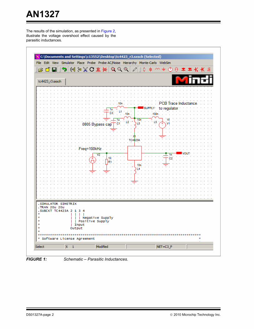
The PCB Trace Inductance diagram in Figure 1 showsthe TC4423A device (3A peak output current) in acircuit with following items:
• L4 – parasitic inductance in series with ground pin
• L5 – parasitic inductance in series with VDD pin
• L1, L2 – parasitic inductance in series with the bypass capacitor
• Capacitor C2 (1 nF) is used to represent the MOSFET
• L3 – the inductance from the TC4423A device to the power source
Note that the inductance between the driver output andC2 (MOSFET) is not included in this circuit simulation,but should be included in common practice. Addition-ally, the driver should be located as close to the outputMOSFET as possible.
GETTING STARTED
Before simulation can begin, a symbol for the MOSFETdriver must be created, and a MOSFET driver modelnetlist must be assigned to that symbol. Pressing theF11 key in Mindi opens a window where the modelnetlist can be copied, and the symbol can be assignedto that model netlist.
For example, assume that the following characteristicsare applied to the items in the simulated circuit inFigure 1:
• L4 and L5 – SOIC package leads PCB trace = 10 nH
• L1 and L2 – series inductance of a 0805 ceramic capacitor PCB trace = 10 nH
• L3 – PCB trace inductance from the VDD pin to the power source that feeds the MOSFET driver
Note that the parasitic series resistance and input/out-put PCB inductance have been omitted from thissimulation, but they are available for inclusion.
Author: Ray DiSilvestroMicrochip Technology Inc.
2010 Microchip Technology Inc. DS01327A-page 1
AN1327
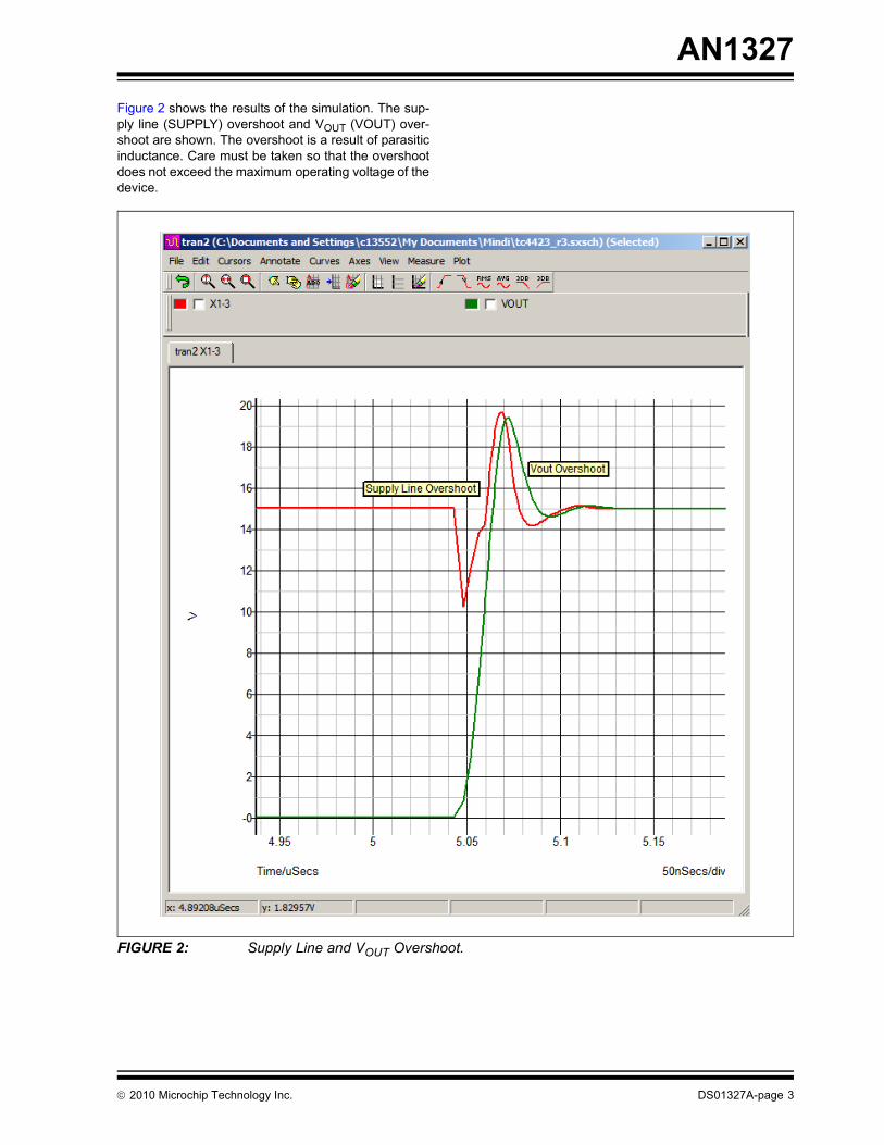
The results of the simulation, as presented in Figure 2,illustrate the voltage overshoot effect caused by theparasitic inductances.
FIGURE 1: Schematic – Parasitic Inductances.
DS01327A-page 2 2010 Microchip Technology Inc.
AN1327
Figure 2 shows the results of the simulation. The sup-ply line (SUPPLY) overshoot and VOUT (VOUT) over-shoot are shown. The overshoot is a result of parasiticinductance. Care must be taken so that the overshootdoes not exceed the maximum operating voltage of thedevice.
FIGURE 2: Supply Line and VOUT Overshoot.
2010 Microchip Technology Inc. DS01327A-page 3
AN1327
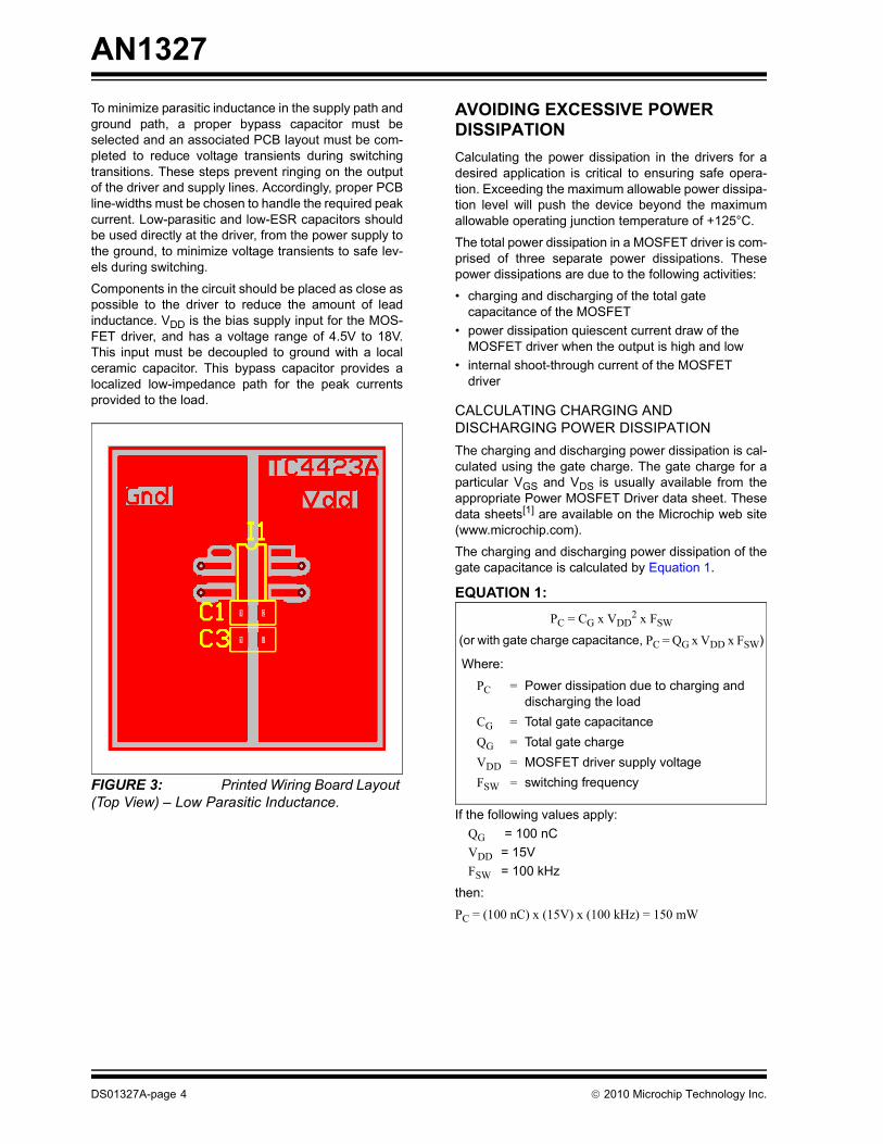
To minimize parasitic inductance in the supply path andground path, a proper bypass capacitor must beselected and an associated PCB layout must be com-pleted to reduce voltage transients during switchingtransitions. These steps prevent ringing on the outputof the driver and supply lines. Accordingly, proper PCBline-widths must be chosen to handle the required peakcurrent. Low-parasitic and low-ESR capacitors shouldbe used directly at the driver, from the power supply tothe ground, to minimize voltage transients to safe lev-els during switching.
Components in the circuit should be placed as close aspossible to the driver to reduce the amount of leadinductance. VDD is the bias supply input for the MOS-FET driver, and has a voltage range of 4.5V to 18V.This input must be decoupled to ground with a localceramic capacitor. This bypass capacitor provides alocalized low-impedance path for the peak currentsprovided to the load.
FIGURE 3: Printed Wiring Board Layout (Top View) – Low Parasitic Inductance.
AVOIDING EXCESSIVE POWER DISSIPATION
Calculating the power dissipation in the drivers for adesired application is critical to ensuring safe opera-tion. Exceeding the maximum allowable power dissipa-tion level will push the device beyond the maximumallowable operating junction temperature of +125°C.
The total power dissipation in a MOSFET driver is com-prised of three separate power dissipations. Thesepower dissipations are due to the following activities:
• charging and discharging of the total gate capacitance of the MOSFET
• power dissipation quiescent current draw of the MOSFET driver when the output is high and low
• internal shoot-through current of the MOSFET driver
CALCULATING CHARGING AND DISCHARGING POWER DISSIPATION
The charging and discharging power dissipation is cal-culated using the gate charge. The gate charge for aparticular VGS and VDS is usually available from theappropriate Power MOSFET Driver data sheet. Thesedata sheets[1] are available on the Microchip web site(www.microchip.com).
The charging and discharging power dissipation of thegate capacitance is calculated by Equation 1.
EQUATION 1:
If the following values apply:
QG = 100 nC
VDD = 15V
FSW = 100 kHz
then:
PC = (100 nC) x (15V) x (100 kHz) = 150 mW
PC = CG x VDD2 x FSW
(or with gate charge capacitance, PC = QG x VDD x FSW)
Where:
PC = Power dissipation due to charging and discharging the load
CG = Total gate capacitance
QG = Total gate charge
VDD = MOSFET driver supply voltage
FSW = switching frequency
DS01327A-page 4 2010 Microchip Technology Inc.
AN1327
CALCULATING QUIESCENT CURRENT DRAW POWER DISSIPATION
The quiescent current draw power dissipation iscalculated through use of Equation 2.
EQUATION 2:
If the following values apply:
IQH = .5 mA
IQL = 50 µA
D = 50%
VDD = 15V
then:
PQ = (0.5 mA x .5 + 50 µA x (1 - .5)) x 15V = 4.125 mW
CALCULATING SHOOT-THROUGH CURRENT POWER DISSIPATION
The shoot-through current power dissipation is calcu-lated from the crossover energy. The crossover energyis usually available in the appropriate data sheet.
The shoot-through current power dissipation iscalculated through use of Equation 3.
EQUATION 3:
If the following values apply:
VDD = 15V
FSW = 100 kHz
CC = 47 nA/sec
then:
PS = (47 nA x sec) x (100 kHz) x (15V) = 70.5 mW
The total power dissipated is:
PT = PC + PQ + PS = 150 mW + 4.125 mW + 70.5 mW =224.63 mW
This value is less than the maximum power dissipationof the device.
CALCULATING INTERNAL JUNCTION TEMPERATURE
The internal junction temperature rise is a function ofinternal power dissipation and the thermal resistance,from junction to ambient, for the application.
A value for thermal resistance from junction to ambient(RθJA) is derived from JESD51-7[2], the EIA/JEDECStandard for measuring thermal resistance of smallsurface mount packages. The standard describes thetest method and board specifications for measuring thethermal resistance from junction to ambient. The actualthermal resistance for a particular application can vary,depending on many factors, such as the amount ofcopper traces on the board and thickness of the layers.
EQUATION 4:
To estimate the internal junction temperature, the cal-culated temperature rise is added to the ambient or off-set temperature. For this example, the worst-casejunction temperature is estimated using Equation 5.
EQUATION 5:
Maximum package power dissipation at +40°C ambienttemperature is derived from Equation 6.
EQUATION 6:
AVOIDING LATCH-UP
Latch-up occurs in CMOS technologies due to parasitictransistors that form a silicon controlled rectifier (SCR).Once triggered, the parasitic SCR turns on and shortsVDD to ground, usually destroying the CMOS device.Microchip application note AN763 – “Latch-Up Protec-tion For MOSFET Drivers”[3], describes in detail thelatch-up effect and how to prevent it.
PQ = (IQH x D + IQL x (1 - D)) x VDD
Where:
PQ = Power dissipated due to the quiescent current draw
IQH = Quiescent current draw with the input in high state
IQL = Quiescent current draw with the input in low state
D = Duty Cycle
VDD = MOSFET driver supply voltage
PS = CC x FSW x VDDWhere:
PS = Power dissipation due to the shoot-through current
CC = Crossover energy constant
FSW = Switching frequency
VDD = MOSFET driver supply voltage
TJ(RISE) = PTOTAL x RθJA
TJRISE = 224.63 mW x 155.0°C/Watt
TJRISE = 34.82°C
TJ = TJRISE + TA(MAX)
TJ = 74.72°C
TA = 40°C
SOIC (155°C/Watt = RθJA)
PD(MAX) = (TA(MAX) - TA)/RθJA
PD(MAX) = (125°C - 40°C)/155°C/W
PD(MAX) = 548 mW
2010 Microchip Technology Inc. DS01327A-page 5
AN1327
CONCLUSIONS
Avoid supply voltages exceeding the absolute maxi-mum ratings. Ratings of the maximum voltage that canbe applied safely to a particular device are supplied inthe corresponding data sheet. Anything in excess ofthat voltage may result in electrical overstress of aninternal junction, and damage to the device. In addition,operation of the device under conditions that are closeto the maximum ratings may degrade long-termreliability.
It is important to note that these ratings apply at alltimes, including those intervals when the device isbeing powered on and off. The triggering mode couldresult from transients on supply lines. Care should betaken to ensure that the maximum ratings are notexceeded.
Also avoid input/output pin voltage that exceeds eithersupply line by more than a diode drop. This could occuras a result of transients on input/output line. Careshould be taken to ensure that the maximum ratingsare not exceeded.
Avoid improper power-supply sequencing. Latch-upcan occur from improper power-supply sequencing indevices that have multiple power supplies. It is possiblefor the maximum ratings to be exceeded and the deviceto enter a latch-up state, in some cases, when thedigital supply is applied prior to other supplies. For thisreason, care should be taken to ensure the maximumratings are not exceeded.
Microchip application note AN763 recommends the fol-lowing course of action, summarized below, to preventlatch-up:
• properly decouple IC
• clamp outputs with diodes when driving inductive loads
• clamp inputs with diodes if input signal exceeds the negative or positive rails of the power supply
• use star grounds, if at all possible, in high current applications
REFERENCES
[1] Tiny 1.5A, High-Speed Power MOSFET DriverData Sheet (DS22092) Microchip TechnologyInc., 2008.
4.0A Dual High-Speed Power MOSFET DriversWith Enable Data Sheet (DS22062) MicrochipTechnology Inc., 2008.
2A Synchronous Buck Power MOSFET DriverData Sheet (DS220830) Microchip TechnologyInc., 2008.
Tiny 500 mA, High-Speed Power MOSFETDriver Data Sheet (DS22052) Microchip Tech-nology Inc., 2007.
4.5A Dual High-Speed Power MOSFET DriversData Sheet (DS22022) Microchip TechnologyInc., 2007.
3A Dual High-Speed Power MOSFET DriversData Sheet (DS21998), Microchip TechnologyInc., 2007.
[2] EIA/JEDEC Standard JESD51-7, “High Effec-tive Thermal Conductivity Test Board for LeadedSurface Mount Packages”, Electronic IndustriesAlliance, February 1999.
[3] Latch-Up Protection For MOSFET Drivers Appli-cation Note AN763 (DS00763), MicrochipTechnology Inc., 2009.
DS01327A-page 6 2010 Microchip Technology Inc.
AN1327
Software License AgreementThe software supplied herewith by Microchip Technology Incorporated (the “Company”) is intended and supplied to you, theCompany’s customer, for use solely and exclusively with products manufactured by the Company.The software is owned by the Company and/or its supplier, and is protected under applicable copyright laws. All rights are reserved.Any use in violation of the foregoing restrictions may subject the user to criminal sanctions under applicable laws, as well as to civilliability for the breach of the terms and conditions of this license.THIS SOFTWARE IS PROVIDED IN AN “AS IS” CONDITION. NO WARRANTIES, WHETHER EXPRESS, IMPLIED OR STATU-TORY, INCLUDING, BUT NOT LIMITED TO, IMPLIED WARRANTIES OF MERCHANTABILITY AND FITNESS FOR A PARTICU-LAR PURPOSE APPLY TO THIS SOFTWARE. THE COMPANY SHALL NOT, IN ANY CIRCUMSTANCES, BE LIABLE FORSPECIAL, INCIDENTAL OR CONSEQUENTIAL DAMAGES, FOR ANY REASON WHATSOEVER.
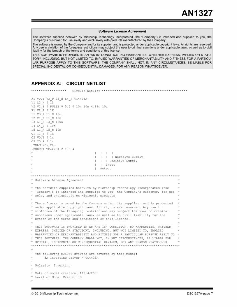
APPENDIX A: CIRCUIT NETLIST
******************* Circuit Netlist **********************************************
X1 VOUT V2_P L5_N L4_P TC4423AV1 L3_N 0 15V2 V2_P 0 PULSE 0 5.5 0 10n 10n 4.99u 10uR1 V2_P 0 1KL1 C3_P L1_N 10n L2 C1_P L1_N 10n L3 L1_N L3_N 100n L4 L4_P 0 10n L5 L1_N L5_N 10n C1 C1_P 0 1u C2 VOUT 0 1n C3 C3_P 0 1u .TRAN 20u 20u.SUBCKT TC4423A 2 1 3 4* | | | | * | | | | Negative Supply* | | | Positive Supply* | | Input* | Output********************************************************************************** Software License Agreement ** ** The software supplied herewith by Microchip Technology Incorporated (the ** 'Company') is intended and supplied to you, the Company's customer, for use ** soley and exclusively on Microchip products. ** ** The software is owned by the Company and/or its supplier, and is protected ** under applicable copyright laws. All rights are reserved. Any use in ** violation of the foregoing restrictions may subject the user to criminal ** sanctions under applicable laws, as well as to civil liability for the ** breach of the terms and conditions of this license. ** ** THIS SOFTWARE IS PROVIDED IN AN 'AS IS' CONDITION. NO WARRANTIES, WHETHER ** EXPRESS, IMPLIED OR STATUTORY, INCLUDING, BUT NOT LIMITED TO, IMPLIED ** WARRANTIES OF MERCHANTABILITY AND FITNESS FOR A PARTICULAR PURPOSE APPLY TO ** THIS SOFTWARE. THE COMPANY SHALL NOT, IN ANY CIRCUMSTANCES, BE LIABLE FOR ** SPECIAL, INCIDENTAL OR CONSEQUENTIAL DAMAGES, FOR ANY REASON WHATSOEVER. *********************************************************************************** The following MOSFET drivers are covered by this model:* 3A Inverting Driver - TC4423A** Polarity: Inverting** Date of model creation: 11/14/2008* Level of Model Creator: G*
2010 Microchip Technology Inc. DS01327A-page 7
AN1327
* Revision History:* 11/14/08 RAW Initial model creation* 11/20/08 RAW Adjusts to rise/fall times* * * * ** Recommendations:* Use PSPICE (or SPICE 2G6; other simulators may require translation)* For a quick, effective design, use a combination of: data sheet* specs, bench testing, and simulations with this macromodel* For high impedance circuits, set GMIN=100F in the .OPTIONS statement** Supported:* Typical performance for temperature range (-40 to 125) degrees Celsius* DC, AC, Transient, and Noise analyses.* Most specs, including: propgation delays, rise times, fall times, max sink/source current,* input thresholds, voltage ranges, supply current, ... , etc.* Temperature effects for Ibias, Iquiescent, output current, output * resistance,....,etc.** Not Supported:* Some Variation in specs vs. Power Supply Voltage* Vos distribution, Ib distribution for Monte Carlo* Some Temperature analysis* Process variation* Behavior outside normal operating region** Known Discrepancies in Model vs. Datasheet:* * ** Input Impedance/ClampR1 4 1 100MEGC1 4 1 20.0PG3 3 1 TABLE { V(3, 1) } ((-770M,-1.00)(-700M,-10.0M)(-630M,-1.00N)(0,0)(20.0,1.00N))G4 1 4 TABLE { V(1, 4) } ((-5.94,-1.00)(-5.4,-10.0M)(-4.86,-1.00N)(0,0)(20.0,1.00N))* ThresholdG11 0 30 TABLE { V(1, 11) } ( (-1m,10n)(0,0)(0.78,-.1)(1.25,-1)(2,-1) )G12 0 30 TABLE {V(1,12)} ( (-2,1)(-1.2,1)(-0.6,.1)(0,0)(1,-10n))G21 0 11 TABLE { V(3, 4) } ((0,1.35)(4.00,1.35)(6.00,1.5)(10.0,1.48)(13.0,1.49)(16.0,1.5))G22 0 12 TABLE { V(3, 4) } ((0,1.35)(4.00,1.16)(6.00,1.25)(10.0,1.24)(13.0,1.24)(16.0,1.25))R21 0 11 1 TC 504U 2.33UR22 0 12 1 TC 231U -103NC30 30 0 1n * HL CircuitG31 0 31 TABLE { V(3, 4) } ((0,170)(4.5,80)(10.0,46.2)(12.0,39.1)(14.0,35.8)(18.0,35.1))R31 31 0 1 TC 2.42M -3.91UG33 0 30 TABLE { V(31, 30) } ( (-1M,-10)(0,0)(1,10N) )S31 31 30 31 30 SS31* LH CircuitG32 32 0 TABLE { V(3, 4) } ((0,190)(4.5,52)(5,67)(10.0,41.0)(12.0,38.6)(14.0,34.5)(18.0,36.8))R32 0 32 1 TC 2.50M 1.09UG34 30 0 TABLE { V(30, 32) } ( (-1M,-10)(0,0)(1,10N) )R30 32 30 1MEG * DRIVEG51 0 50 TABLE { V(30, 0) } ( (-5,-1U)(-3,-1U)(0,0)(6,4)(18,4.1) )G52 50 0 TABLE { V(0, 30) } ( (-5,-1U)(-3,-1U)(0,0)(6,3.5)(18,3.6) )R53 0 50 1G50 51 60 VALUE {V(50,0)*300M/(-700M+18.0/(V(3,4) + 1M))}R51 51 0 1G53 3 0 TABLE {V(51,0)} ((-100,100)(0,0)(1,1n)) G54 0 4 TABLE {V(0,51)} ((-100,100)(0,0)(1,1n))
DS01327A-page 8 2010 Microchip Technology Inc.
AN1327
R60 0 60 100MEG H67 0 69 V67 1V67 60 59 0VC60 561 60 1000PR59 59 2 1.28L59 59 2 5.0N* Shoot-through adjustmentVC60 56 0 0VRC60 56 561 1mH60 58 0 VC60 56G60P 0 3 TABLE { V(58, 0) } ((-1,-1u)(0,0)(20,0)(200,-2))G60N 4 0 TABLE { V(0, 58) } ((-1,-1u)(0,0)(20,0)(200,-2))* Source OutputE67 67 0 TABLE { V(69, 0) } ( (-4.5,-4.5)(0,0)(1,2.00) )G63 0 63 POLY(1) 3 4 6.81 -439M 12.9MR63 0 63 1 TC 3.45M -4.18UE61 61 65 VALUE {V(67,0)*V(63,0)}V63 65 3 100UG61 61 60 TABLE { V(61, 60) } (-20.0M,-450)(-15.0M,-225)(-10.0M,-45.0)(0,0)(10,1N))* Sink OutputE68 68 0 TABLE { V(69, 0) } ( (-1,-2.00)(0,0)(4.5,4.5) )G64 0 64 POLY(1) 3 4 6.49 -455M 12.6MR64 0 64 1 TC 3.18M -5.83UE62 62 66 VALUE {V(68,0)*V(64,0)}V64 66 4 100UG62 60 62 TABLE { V(60, 62) } (-20.0M,-450)(-15.0M,-225)(-10.0M,-45.0)(0,0)(10,1N))* Bias CurrentG55 0 55 TABLE { V(3, 4) } ((0,0)(4.5,75.0U)(10.0,97.5U)(14.0,120U)(18.0,145U))G56 3 4 55 0 1R55 55 0 1 TC 2.49M -16.9UG57 0 57 TABLE { V(3, 4) } ((0,0)(4.5,35.0U)(10.0,37.5U)(14.0,40.0U)(18.0,40.0U))G58 3 4 57 0 1R57 57 0 1 TC 1.03M 15.4US59 55 0 1 0 SS59* Models.MODEL SS59 VSWITCH Roff=1m Ron=100Meg Voff=1.2V Von=1.5V.MODEL SS31 VSWITCH Roff=100MEG Ron=800 Voff=0.2V Von=0.1V.ENDS
2010 Microchip Technology Inc. DS01327A-page 9
AN1327
NOTES:
DS01327A-page 10 2010 Microchip Technology Inc.
Note the following details of the code protection feature on Microchip devices:
• Microchip products meet the specification contained in their particular Microchip Data Sheet.
• Microchip believes that its family of products is one of the most secure families of its kind on the market today, when used in the intended manner and under normal conditions.
• There are dishonest and possibly illegal methods used to breach the code protection feature. All of these methods, to our knowledge, require using the Microchip products in a manner outside the operating specifications contained in Microchip’s Data Sheets. Most likely, the person doing so is engaged in theft of intellectual property.
• Microchip is willing to work with the customer who is concerned about the integrity of their code.
• Neither Microchip nor any other semiconductor manufacturer can guarantee the security of their code. Code protection does not mean that we are guaranteeing the product as “unbreakable.”
Code protection is constantly evolving. We at Microchip are committed to continuously improving the code protection features of ourproducts. Attempts to break Microchip’s code protection feature may be a violation of the Digital Millennium Copyright Act. If such actsallow unauthorized access to your software or other copyrighted work, you may have a right to sue for relief under that Act.
Information contained in this publication regarding deviceapplications and the like is provided only for your convenienceand may be superseded by updates. It is your responsibility toensure that your application meets with your specifications.MICROCHIP MAKES NO REPRESENTATIONS ORWARRANTIES OF ANY KIND WHETHER EXPRESS ORIMPLIED, WRITTEN OR ORAL, STATUTORY OROTHERWISE, RELATED TO THE INFORMATION,INCLUDING BUT NOT LIMITED TO ITS CONDITION,QUALITY, PERFORMANCE, MERCHANTABILITY ORFITNESS FOR PURPOSE. Microchip disclaims all liabilityarising from this information and its use. Use of Microchipdevices in life support and/or safety applications is entirely atthe buyer’s risk, and the buyer agrees to defend, indemnify andhold harmless Microchip from any and all damages, claims,suits, or expenses resulting from such use. No licenses areconveyed, implicitly or otherwise, under any Microchipintellectual property rights.
2010 Microchip Technology Inc.
Trademarks
The Microchip name and logo, the Microchip logo, dsPIC, KEELOQ, KEELOQ logo, MPLAB, PIC, PICmicro, PICSTART, PIC32 logo, rfPIC and UNI/O are registered trademarks of Microchip Technology Incorporated in the U.S.A. and other countries.
FilterLab, Hampshire, HI-TECH C, Linear Active Thermistor, MXDEV, MXLAB, SEEVAL and The Embedded Control Solutions Company are registered trademarks of Microchip Technology Incorporated in the U.S.A.
Analog-for-the-Digital Age, Application Maestro, CodeGuard, dsPICDEM, dsPICDEM.net, dsPICworks, dsSPEAK, ECAN, ECONOMONITOR, FanSense, HI-TIDE, In-Circuit Serial Programming, ICSP, Mindi, MiWi, MPASM, MPLAB Certified logo, MPLIB, MPLINK, mTouch, Octopus, Omniscient Code Generation, PICC, PICC-18, PICDEM, PICDEM.net, PICkit, PICtail, REAL ICE, rfLAB, Select Mode, Total Endurance, TSHARC, UniWinDriver, WiperLock and ZENA are trademarks of Microchip Technology Incorporated in the U.S.A. and other countries.
SQTP is a service mark of Microchip Technology Incorporated in the U.S.A.
All other trademarks mentioned herein are property of their respective companies.
© 2010, Microchip Technology Incorporated, Printed in the U.S.A., All Rights Reserved.
Printed on recycled paper.
ISBN: 978-1-60932-266-3
DS01327A-page 11
Microchip received ISO/TS-16949:2002 certification for its worldwide headquarters, design and wafer fabrication facilities in Chandler and Tempe, Arizona; Gresham, Oregon and design centers in California and India. The Company’s quality system processes and procedures are for its PIC® MCUs and dsPIC® DSCs, KEELOQ® code hopping devices, Serial EEPROMs, microperipherals, nonvolatile memory and analog products. In addition, Microchip’s quality system for the design and manufacture of development systems is ISO 9001:2000 certified.

DS01327A-page 12 2010 Microchip Technology Inc.
AMERICASCorporate Office2355 West Chandler Blvd.Chandler, AZ 85224-6199Tel: 480-792-7200 Fax: 480-792-7277Technical Support: http://support.microchip.comWeb Address: www.microchip.com
AtlantaDuluth, GA Tel: 678-957-9614 Fax: 678-957-1455
BostonWestborough, MA Tel: 774-760-0087 Fax: 774-760-0088
ChicagoItasca, IL Tel: 630-285-0071 Fax: 630-285-0075
ClevelandIndependence, OH Tel: 216-447-0464 Fax: 216-447-0643
DallasAddison, TX Tel: 972-818-7423 Fax: 972-818-2924
DetroitFarmington Hills, MI Tel: 248-538-2250Fax: 248-538-2260
KokomoKokomo, IN Tel: 765-864-8360Fax: 765-864-8387
Los AngelesMission Viejo, CA Tel: 949-462-9523 Fax: 949-462-9608
Santa ClaraSanta Clara, CA Tel: 408-961-6444Fax: 408-961-6445
TorontoMississauga, Ontario, CanadaTel: 905-673-0699 Fax: 905-673-6509
ASIA/PACIFICAsia Pacific OfficeSuites 3707-14, 37th FloorTower 6, The GatewayHarbour City, KowloonHong KongTel: 852-2401-1200Fax: 852-2401-3431
Australia - SydneyTel: 61-2-9868-6733Fax: 61-2-9868-6755
China - BeijingTel: 86-10-8528-2100 Fax: 86-10-8528-2104
China - ChengduTel: 86-28-8665-5511Fax: 86-28-8665-7889
China - ChongqingTel: 86-23-8980-9588Fax: 86-23-8980-9500
China - Hong Kong SARTel: 852-2401-1200 Fax: 852-2401-3431
China - NanjingTel: 86-25-8473-2460Fax: 86-25-8473-2470
China - QingdaoTel: 86-532-8502-7355Fax: 86-532-8502-7205
China - ShanghaiTel: 86-21-5407-5533 Fax: 86-21-5407-5066
China - ShenyangTel: 86-24-2334-2829Fax: 86-24-2334-2393
China - ShenzhenTel: 86-755-8203-2660 Fax: 86-755-8203-1760
China - WuhanTel: 86-27-5980-5300Fax: 86-27-5980-5118
China - XianTel: 86-29-8833-7252Fax: 86-29-8833-7256
China - XiamenTel: 86-592-2388138 Fax: 86-592-2388130
China - ZhuhaiTel: 86-756-3210040 Fax: 86-756-3210049
ASIA/PACIFICIndia - BangaloreTel: 91-80-3090-4444 Fax: 91-80-3090-4123
India - New DelhiTel: 91-11-4160-8631Fax: 91-11-4160-8632
India - PuneTel: 91-20-2566-1512Fax: 91-20-2566-1513
Japan - YokohamaTel: 81-45-471- 6166 Fax: 81-45-471-6122
Korea - DaeguTel: 82-53-744-4301Fax: 82-53-744-4302
Korea - SeoulTel: 82-2-554-7200Fax: 82-2-558-5932 or 82-2-558-5934
Malaysia - Kuala LumpurTel: 60-3-6201-9857Fax: 60-3-6201-9859
Malaysia - PenangTel: 60-4-227-8870Fax: 60-4-227-4068
Philippines - ManilaTel: 63-2-634-9065Fax: 63-2-634-9069
SingaporeTel: 65-6334-8870Fax: 65-6334-8850
Taiwan - Hsin ChuTel: 886-3-6578-300Fax: 886-3-6578-370
Taiwan - KaohsiungTel: 886-7-536-4818Fax: 886-7-536-4803
Taiwan - TaipeiTel: 886-2-2500-6610 Fax: 886-2-2508-0102
Thailand - BangkokTel: 66-2-694-1351Fax: 66-2-694-1350
EUROPEAustria - WelsTel: 43-7242-2244-39Fax: 43-7242-2244-393Denmark - CopenhagenTel: 45-4450-2828 Fax: 45-4485-2829
France - ParisTel: 33-1-69-53-63-20 Fax: 33-1-69-30-90-79
Germany - MunichTel: 49-89-627-144-0 Fax: 49-89-627-144-44
Italy - Milan Tel: 39-0331-742611 Fax: 39-0331-466781
Netherlands - DrunenTel: 31-416-690399 Fax: 31-416-690340
Spain - MadridTel: 34-91-708-08-90Fax: 34-91-708-08-91
UK - WokinghamTel: 44-118-921-5869Fax: 44-118-921-5820
WORLDWIDE SALES AND SERVICE
01/05/10