Embed Size (px)
Citation preview
32000D–04/2011
AVR32
Architecture Document
Feature Summary• 32-bit load/store RISC architecture• Up to 15 general-purpose 32-bit registers• 32-bit Stack Pointer, Program Counter, and Link Register reside in register file• Fully orthogonal instruction set• Pipelined architecture allows one instruction per clock cycle for most instructions• Byte, half-word, word and double word memory access• Fast interrupts and multiple interrupt priority levels• Optional branch prediction for minimum delay branches• Privileged and unprivileged modes enabling efficient and secure Operating Systems• Innovative instruction set together with variable instruction length ensuring industry
leading code density• Optional DSP extention with saturated arithmetic, and a wide variety of multiply
instructions• Optional extensions for Java, SIMD, Read-Modify-Write to memory, and Coprocessors• Architectural support for efficient On-Chip Debug solutions• Optional MPU or MMU allows for advanced operating systems• FlashVault™ support through Secure State for executing trusted code alongside
nontrusted code on the same CPU
1. IntroductionAVR32 is a new high-performance 32-bit RISC microprocessor core, designed for cost-sensitiveembedded applications, with particular emphasis on low power consumption and high code den-sity. In addition, the instruction set architecture has been tuned to allow for a variety ofmicroarchitectures, enabling the AVR32 to be implemented as low-, mid- or high-performanceprocessors. AVR32 extends the AVR family into the world of 32- and 64-bit applications.
1.1 The AVR familyThe AVR family was launched by Atmel in 1996 and has had remarkable success in the 8-and16-bit flash microcontroller market. AVR32 is complements the current AVR microcontrollers.Through the AVR32 family, the AVR is extended into a new range of higher performance appli-cations that is currently served by 32- and 64-bit processors
To truly exploit the power of a 32-bit architecture, the new AVR32 architecture is not binary com-patible with earlier AVR architectures. In order to achieve high code density, the instructionformat is flexible providing both compact instructions with 16 bits length and extended 32-bitinstructions. While the instruction length is only 16 bits for most instructions, powerful 32-bitinstructions are implemented to further increase performance. Compact and extended instruc-tions can be freely mixed in the instruction stream.
1.2 The AVR32 Microprocessor ArchitectureThe AVR32 is a new innovative microprocessor architecture. It is a fully synchronous synthesis-able RTL design with industry standard interfaces, ensuring easy integration into SoC designswith legacy intellectual property (IP). Through a quantitative approach, a large set of industryrecognized benchmarks has been compiled and analyzed to achieve the best code density in itsclass of microprocessor architectures. In addition to lowering the memory requirements, a com-pact code size also contributes to the core’s low power characteristics. The processor supportsbyte and half-word data types without penalty in code size and performance.
Memory load and store operations are provided for byte, half-word, word and double word datawith automatic sign- or zero extension of half-word and byte data. The C-compiler is closelylinked to the architecture and is able to exploit code optimization features, both for size andspeed.
In order to reduce code size to a minimum, some instructions have multiple addressing modes.As an example, instructions with immediates often have a compact format with a smaller imme-diate, and an extended format with a larger immediate. In this way, the compiler is able to usethe format giving the smallest code size.
Another feature of the instruction set is that frequently used instructions, like add, have a com-pact format with two operands as well as an extended format with three operands. The largerformat increases performance, allowing an addition and a data move in the same instruction in asingle cycle.
Load and store instructions have several different formats in order to reduce code size andspeed up execution:
• Load/store to an address specified by a pointer register
• Load/store to an address specified by a pointer register with postincrement
232000D–04/2011
AVR32
AVR32
• Load/store to an address specified by a pointer register with predecrement
• Load/store to an address specified by a pointer register with displacement
• Load/store to an address specified by a small immediate (direct addressing within a small page)
• Load/store to an address specified by a pointer register and an index register.
The register file is organized as 16 32-bit registers and includes the Program Counter, the LinkRegister, and the Stack Pointer. In addition, one register is designed to hold return values fromfunction calls and is used implicitly by some instructions.
The AVR32 core defines several micro architectures in order to capture the entire range of appli-cations. The microarchitectures are named AVR32A, AVR32B and so on. Differentmicroarchitectures are suited to different end applications, allowing the designer to select amicroarchitecture with the optimum set of parameters for a specific application.
1.2.1 Exceptions and InterruptsThe AVR32 incorporates a powerful exception handling scheme. The different exceptionsources, like Illegal Op-code and external interrupt requests, have different priority levels, ensur-ing a well-defined behavior when multiple exceptions are received simultaneously. Additionally,pending exceptions of a higher priority class may preempt handling of ongoing exceptions of alower priority class. Each priority class has dedicated registers to keep the return address andstatus register thereby removing the need to perform time-consuming memory operations tosave this information.
There are four levels of external interrupt requests, all executing in their own context. The con-texts can provide a number of dedicated registers for the interrupts to use directly ensuring lowlatency. High priority interrupts may have a larger number of shadow registers available than lowpriority interrupts. An interrupt controller does the priority handling of the external interrupts andprovides the prioritized interrupt vector to the processor core.
1.2.2 Java SupportJava hardware acceleration is available as an option, in the form of a Java Card or Java VirtualMachine hardware implementation.
1.2.3 FlashVaultRevision 3 of the AVR32 architecture introduced a new CPU state called Secure State. Thisstate is instrumental in the new security technology named FlashVault. This innovation allowsthe on-chip flash and other memories to be partially programmed and locked, creating a safe on-chip storage for secret code and valuable software intellectual property. Code stored in theFlashVault will execute as normal, but reading, copying or debugging the code is not possible.This allows a device with FlashVault code protection to carry a piece of valuable software suchas a math library or an encryption algorithm from a trusted location to a potentially untrustworthypartner where the rest of the source code can be developed, debugged and programmed.
332000D–04/2011

1.3 MicroarchitecturesThe AVR32 architecture defines different microarchitectures. This enables implementations thatare tailored to specific needs and applications. The microarchitectures provide different perfor-mance levels at the expense of area and power consumption. The following microarchitecturesare defined:
1.3.1 AVR32AThe AVR32A microarchitecture is targeted at cost-sensitive, lower-end applications like smallermicrocontrollers. This microarchitecture does not provide dedicated hardware registers for shad-owing of register file registers in interrupt contexts. Additionally, it does not provide hardwareregisters for the return address registers and return status registers. Instead, all this informationis stored on the system stack. This saves chip area at the expense of slower interrupt handling.
Upon interrupt initiation, registers R8-R12 are automatically pushed to the system stack. Theseregisters are pushed regardless of the priority level of the pending interrupt. The return addressand status register are also automatically pushed to stack. The interrupt handler can thereforeuse R8-R12 freely. Upon interrupt completion, the old R8-R12 registers and status register arerestored, and execution continues at the return address stored popped from stack.
The stack is also used to store the status register and return address for exceptions and scall.Executing the rete or rets instruction at the completion of an exception or system call will popthis status register and continue execution at the popped return address.
1.3.2 AVR32BThe AVR32B microarchitecture is targeted at applications where interrupt latency is important.The AVR32B therefore implements dedicated registers to hold the status register and returnaddress for interrupts, exceptions and supervisor calls. This information does not need to bewritten to the stack, and latency is therefore reduced. Additionally, AVR32B allows hardwareshadowing of the registers in the register file. The INT0 to INT3 contexts may have dedicatedversions of the registers in the register file, allowing the interrupt routine to start executingimmediately.
The scall, rete and rets instructions use the dedicated status register and return address regis-ters in their operation. No stack accesses are performed.
432000D–04/2011
AVR32
AVR32
2. Programming ModelThis chapter describes the programming model and the set of registers accessible to the user.
2.1 Data FormatsThe AVR32 processor supports the data types shown in Table 2-1 on page 5:
When any of these types are described as unsigned, the N bit data value represents a non-neg-ative integer in the range 0 to + 2N-1.
When any of these types are described as signed, the N bit data value represents an integer inthe range of -2N-1 to +2N-1-1, using two’s complement format.
Some instructions operate on fractional numbers. For these numbers, the data value representsa fraction in the range of -1 to +1-2-(N-1), using two’s complement format.
2.2 Data OrganizationData is usually stored in a big-endian way, see Figure 2-1 on page 5. This means that whenmulti-byte data is stored in memory, the most significant byte is stored at the lowest address. Allinstructions are interpreted as being big-endian. However, in order to support data transfers thatare little-endian, special endian-translating load and store instructions are defined.
The register file can hold data of different formats. Both byte, halfword (16-bit) and word (32-bit)formats can be represented, and byte and halfword formats are supported in both unsigned andsigned 2’s complement formats. Some instructions also use doubleword operands. Doubleworddata are placed in two consecutive registers. The most significant word is in the uppermost reg-ister. Valid register pairs are R1:R0, R3:R2, R5:R4, R7:R6, R9:R8, R11:R10 and R13:R12.
Load and store operations that transfer bytes or halfwords, automatically zero-extends or sign-extends the bytes or half-words as they are loaded.
Figure 2-1. Data representation in the register file
Table 2-1. Overview of execution modes, their priorities and privilege levels.
Type Data Width
Byte 8 bits
Halfword 16 bits
Word 32 bits
Double Word 64 bits
S S S S S S S S S S S S S S S S S S S S S S S S B y teS7 083 1
0 0 0 0 0 0 0 0 0 0 0 0 0 0 0 0 0 0 0 0 0 0 0 0 B y te7 083 1
S S S S S S S S S S S S S S S S1 5 01 63 1
H a lfw o rdS
0 0 0 0 0 0 0 0 0 0 0 0 0 0 0 01 5 01 63 1
H a lfw o rd
to p u p p e r lo w e r b o tto m3 1 0
S ig n e x te n d e d b y te
U n s ig n e d b y te
S ig n e x te n d e d h a lfw o rd
U n s ig n e d h a lfw o rd
W o rd
532000D–04/2011
AVR32 can access data of size byte, halfword, word and doubleword using dedicated instruc-tions. The memory system can support unaligned accesses for selected load/store instructionsin some implementations. Any other unaligned access will cause an address exception.
For performance reasons, the user should make sure that the stack always is word aligned. Thismeans that only word instructions can be used to access the stack. When manipulating thestack pointer, the user has to ensure that the result is word aligned before trying to load andstore data on the stack. Failing to do so will result in performance penalties. Code will executecorrectly if the stack is unaligned but with a significant performance penalty.
2.3 Instruction OrganizationThe AVR32 instruction set has both compact and extended instructions. Compact instructionsdenotes the instructions which have a length of 16 bits while extended instructions have a lengthof 32 bits.
All instructions must be placed on halfword boundaries, see Table 2-2 on page 6. Extendedinstructions can be both aligned and unaligned to halfword boundaries. In normal instructionflow, the instruction buffer will always contain enough entries to ensure that compact, alignedextended and unaligned extended instructions can be issued in a single cycle.
Change-of-flow operations such as branches, jumps, calls and returns may in some implemen-tations require the instruction buffer to be flushed. The user should consult the TechnicalReference Manual for the specific implementation in order to determine how alignment of thebranch target address affects performance.
Table 2-2. Instructions are stored in memory in a big endian fashion and must be aligned on half word boundaries
Word Address
I J N+24
H1 H2 N+20
F2 G N+16
E2 F1 N+12
D E1 N+8
C1 C2 N+4
A B N
Byte Address 0 1 2 3
Byte Address 0 1 2 3
632000D–04/2011
AVR32
AVR32
2.4 Processor States
2.4.1 Normal RISC StateThe AVR32 processor supports several different execution contexts as shown in Table 2-3 onpage 7.
Mode changes can be made under software control, or can be caused by external interrupts orexception processing. A mode can be interrupted by a higher priority mode, but never by onewith lower priority. Nested exceptions can be supported with a minimal software overhead.
When running an operating system on the AVR32, user processes will typically execute in theapplication mode. The programs executed in this mode are restricted from executing certaininstructions. Furthermore, most system registers together with the upper halfword of the statusregister cannot be accessed. Protected memory areas are also not available. All other operatingmodes are privileged and are collectively called System Modes. They have full access to all priv-ileged and unprivileged resources. After a reset, the processor will be in supervisor mode.
2.4.2 Debug StateThe AVR32 can be set in a debug state, which allows implementation of software monitor rou-tines that can read out and alter system information for use during application development. Thisimplies that all system and application registers, including the status registers and programcounters, are accessible in debug state. The privileged instructions are also available.
All interrupt levels are by default disabled when debug state is entered, but they can individuallybe switched on by the monitor routine by clearing the respective mask bit in the status register.
Debug state can be entered as described in the Technical Reference Manual.
Debug state is exited by the retd instruction.
2.4.3 Java StateSome versions of the AVR32 processor core comes with a Java Extension Module (JEM). Theprocessor can be set in a Java State where normal RISC operations are suspended. The Javastate is described in chapter 3.
2.4.4 Secure StateThe secure state added in the AVR32 Architecture revision 3 allows executing secure or trustedsoftware in alongside nonsecure or untrusted software on the same processor. Hardware mech-
Table 2-3. Overview of execution modes, their priorities and privilege levels.
Priority Mode Security Description
1 Non Maskable Interrupt Privileged Non Maskable high priority interrupt mode
2 Exception Privileged Execute exceptions
3 Interrupt 3 Privileged General purpose interrupt mode
4 Interrupt 2 Privileged General purpose interrupt mode
5 Interrupt 1 Privileged General purpose interrupt mode
6 Interrupt 0 Privileged General purpose interrupt mode
N/A Supervisor Privileged Runs supervisor calls
N/A Application Unprivileged Normal program execution mode
732000D–04/2011
anisms are in place to make sure the nonsecure software can not read or modify instruction ordata belonging to the secure software. The secure state is described in chapter 4.
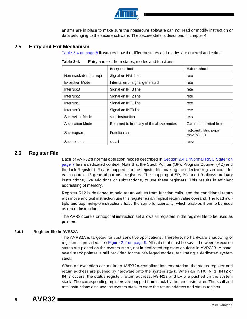
2.5 Entry and Exit MechanismTable 2-4 on page 8 illustrates how the different states and modes are entered and exited.
2.6 Register FileEach of AVR32’s normal operation modes described in Section 2.4.1 “Normal RISC State” onpage 7 has a dedicated context. Note that the Stack Pointer (SP), Program Counter (PC) andthe Link Register (LR) are mapped into the register file, making the effective register count foreach context 13 general purpose registers. The mapping of SP, PC and LR allows ordinaryinstructions, like additions or subtractions, to use these registers. This results in efficientaddressing of memory.
Register R12 is designed to hold return values from function calls, and the conditional returnwith move and test instruction use this register as an implicit return value operand. The load mul-tiple and pop multiple instructions have the same functionality, which enables them to be usedas return instructions.
The AVR32 core’s orthogonal instruction set allows all registers in the register file to be used aspointers.
2.6.1 Register file in AVR32AThe AVR32A is targeted for cost-sensitive applications. Therefore, no hardware-shadowing ofregisters is provided, see Figure 2-2 on page 9. All data that must be saved between executionstates are placed on the system stack, not in dedicated registers as done in AVR32B. A shad-owed stack pointer is still provided for the privileged modes, facilitating a dedicated systemstack.
When an exception occurs in an AVR32A-compliant implementation, the status register andreturn address are pushed by hardware onto the system stack. When an INT0, INT1, INT2 orINT3 occurs, the status register, return address, R8-R12 and LR are pushed on the systemstack. The corresponding registers are popped from stack by the rete instruction. The scall andrets instructions also use the system stack to store the return address and status register.
Table 2-4. Entry and exit from states, modes and functions
Entry method Exit method
Non-maskable Interrupt Signal on NMI line rete
Exception Mode Internal error signal generated rete
Interrupt3 Signal on INT3 line rete
Interrupt2 Signal on INT2 line rete
Interrupt1 Signal on INT1 line rete
Interrupt0 Signal on INT0 line rete
Supervisor Mode scall instruction rets
Application Mode Returned to from any of the above modes Can not be exited from
Subprogram Function callret{cond}, ldm, popm, mov PC, LR
Secure state sscall retss
832000D–04/2011
AVR32

AVR32
Figure 2-2. Register File in AVR32A
2.6.2 Register File in AVR32BThe AVR32B allows separate register files for the interrupt and exception modes, see Figure 2-3on page 9. These modes have a number of implementation defined shadowed registers in orderto speed up interrupt handling. The shadowed registers are automatically mapped in dependingon the current execution mode.
All contexts, except Application, have a dedicated Return Status Register (RSR) and ReturnAddress Register (RAR). The RSR registers are used for storing the Status Register value in thecontext to return to. The RAR registers are used for storing the address in the context to returnto. The RSR and RAR registers eliminates the need to temporarily store the Status Register andreturn address to stack when entering a new context.
Figure 2-3. Register File in AVR32B
The register file is designed with an implementation specific part and an architectural definedpart. Depending on the implementation, each of the interrupt modes can have different configu-
Application
Bit 0
Supervisor
Bit 31
PC
SR
INT0PC
FINTPCINT1PC
SMPC
R7
R5R6
R4R3
R1R2
R0
Bit 0Bit 31
PC
SR
R12
INT0PC
FINTPCINT1PC
SMPC
R7
R5R6
R4
R11
R9R10
R8
R3
R1R2
R0
INT0
SP_APP SP_SYSR12R11
R9R10
R8
Exception NMIINT1 INT2 INT3
LRLR
Bit 0Bit 31
PC
SR
R12
INT0PC
FINTPCINT1PC
SMPC
R7
R5R6
R4
R11
R9R10
R8
R3
R1R2
R0
SP_SYSLR
Bit 0Bit 31
PC
SR
R12
INT0PC
FINTPCINT1PC
SMPC
R7
R5R6
R4
R11
R9R10
R8
R3
R1R2
R0
SP_SYSLR
Bit 0Bit 31
PC
SR
R12
INT0PC
FINTPCINT1PC
SMPC
R7
R5R6
R4
R11
R9R10
R8
R3
R1R2
R0
SP_SYSLR
Bit 0Bit 31
PC
SR
R12
INT0PC
FINTPCINT1PC
SMPC
R7
R5R6
R4
R11
R9R10
R8
R3
R1R2
R0
SP_SYSLR
Bit 0Bit 31
PC
SR
R12
INT0PC
FINTPCINT1PC
SMPC
R7
R5R6
R4
R11
R9R10
R8
R3
R1R2
R0
SP_SYSLR
Bit 0Bit 31
PC
SR
R12
INT0PC
FINTPCINT1PC
SMPC
R7
R5R6
R4
R11
R9R10
R8
R3
R1R2
R0
SP_SYSLR
Application
Bit 0
Supervisor
Bit 31
PC
SR
INT0PC
FINTPCINT1PC
SMPC
R7
R5R6
R4R3
R1R2
R0
Bit 0Bit 31
PC
SR
R12
INT0PC
FINTPCINT1PC
SMPC
R7
R5R6
R4
R11
R9R10
R8
R3
R1R2
R0
INT0
Bit 0Bit 31
PC
RSR_INT0SR
SP_APP SP_SYS SP_SYSR12R11
R9R10
R8banked
registers(implementation
defined)
Bit 0Bit 31
PCLR / LR_INT2
SP_SYS
banked registers
(implementation defined)
RSR_INT2SR
Bit 0Bit 31
PC
RSR_INT3
LR / LR_INT3
SR
SP_SYS
banked registers
(implementation defined)
Bit 0Bit 31
PC
SR
SP_SYS
banked registers
(implementation defined)
RSR_INT1
Exception
Bit 0Bit 31
PC
SR
R12
INT0PC
FINTPCINT1PC
SMPC
R7
R5R6
R4
R11
R9R10
R8
R3
R1R2
R0
SP_SYSLR
RSR_EX
NMI
Bit 0Bit 31
PC
SR
R12
INT0PC
FINTPCINT1PC
SMPC
R7
R5R6
R4
R11
R9R10
R8
R3
R1R2
R0
SP_SYSLR
RSR_NMI
INT1 INT2 INT3
LRLR
RSR_SUP
LR / LR_INT0 LR / LR_INT1
RAR_INT0 RAR_INT2 RAR_INT3RAR_INT1 RAR_EX RAR_NMIRAR_SUP
932000D–04/2011
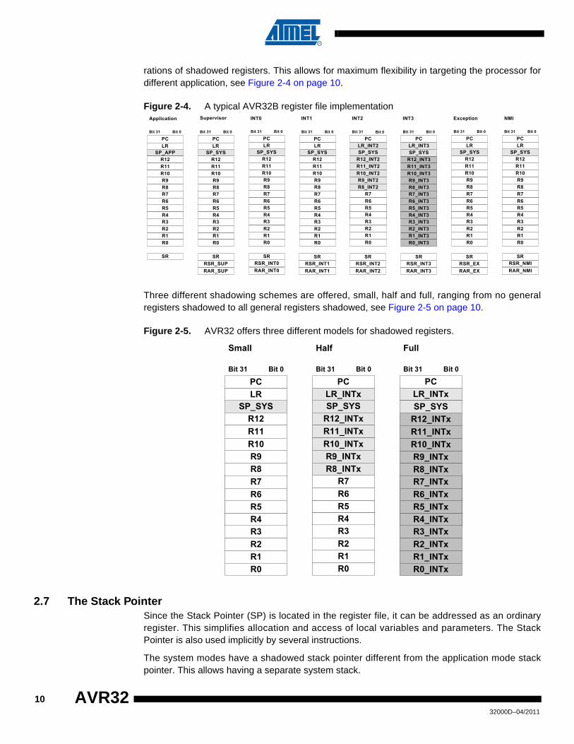
rations of shadowed registers. This allows for maximum flexibility in targeting the processor fordifferent application, see Figure 2-4 on page 10.
Figure 2-4. A typical AVR32B register file implementation
Three different shadowing schemes are offered, small, half and full, ranging from no generalregisters shadowed to all general registers shadowed, see Figure 2-5 on page 10.
Figure 2-5. AVR32 offers three different models for shadowed registers.
2.7 The Stack PointerSince the Stack Pointer (SP) is located in the register file, it can be addressed as an ordinaryregister. This simplifies allocation and access of local variables and parameters. The StackPointer is also used implicitly by several instructions.
The system modes have a shadowed stack pointer different from the application mode stackpointer. This allows having a separate system stack.
Application
Bit 0
Supervisor
Bit 31
PC
SR
INT0PC
FINTPCINT1PC
SMPC
R7
R5R6
R4R3
R1R2
R0
Bit 0Bit 31
PC
SR
R12
INT0PC
FINTPCINT1PC
SMPC
R7
R5R6
R4
R11
R9R10
R8
R3
R1R2
R0
RSR_INT0SR
RSR_EXSR
SP_APP SP_SYS
RSR_NMISR
R12R11
R9R10
R8
Bit 0Bit 31
PCLR
INT0PC
FINTPCINT1PC
SMPC
R7
R5R6
R4R3
R1R2
R0
Bit 0Bit 31
PCLR_INT2
FINTPCSMPC
R7
R5R6
R4R3
R1R2
R0
Bit 0Bit 31
PCLR_INT3
R12_INT3
INT0PC
FINTPCINT1PC
SMPC
R7_INT3
R5_INT3R6_INT3
R4_INT3
R11_INT3
R9_INT3R10_INT3
R8_INT3
R3_INT3
R1_INT3R2_INT3
R0_INT3
SP_SYS SP_SYS SP_SYSR12R11
R9R10
R8
R12_INT2R11_INT2
R9_INT2R10_INT2
R8_INT2
Bit 0Bit 31
PCLR
INT0PC
FINTPCINT1PC
SMPC
R7
R5R6
R4R3
R1R2
R0
SP_SYSR12R11
R9R10
R8
Bit 0Bit 31
PCLR
INT0PC
FINTPCINT1PC
SMPC
R7
R5R6
R4R3
R1R2
R0
SP_SYSR12R11
R9R10
R8
Bit 0Bit 31
PCLR
INT0PC
FINTPCINT1PC
SMPC
R7
R5R6
R4R3
R1R2
R0
SP_SYSR12R11
R9R10
R8
RSR_INT1SR
RSR_INT2SR
RSR_INT3SR
INT0 INT1 INT2 INT3 Exception NMI
RSR_SUP
LRLR
RAR_INT0 RAR_EX RAR_NMIRAR_INT1 RAR_INT2 RAR_INT3RAR_SUP
Small
Bit 0Bit 31
PCLR
INT0PC
FINTPCINT1PC
SMPC
R7
R5R6
R4R3
R1R2
R0
Half
Bit 0Bit 31
PCLR_INTx
FINTPCSMPC
R7
R5R6
R4R3
R1R2
R0
Full
Bit 0Bit 31
PCLR_INTx
R12_INTx
INT0PC
FINTPCINT1PC
SMPC
R7_INTx
R5_INTxR6_INTx
R4_INTx
R11_INTx
R9_INTxR10_INTx
R8_INTx
R3_INTx
R1_INTxR2_INTx
R0_INTx
SP_SYS SP_SYS SP_SYSR12R11
R9R10
R8
R12_INTxR11_INTx
R9_INTxR10_INTx
R8_INTx
1032000D–04/2011
AVR32
AVR32
2.8 The Program CounterThe Program Counter (PC) contains the address of the instruction being executed. The memoryspace is byte addressed. With the exception of Java state, the instruction size is a multiple of 2bytes and the LSB of the Program Counter is fixed to zero. The PC is automatically incrementedin normal program flow, depending on the size of the current instruction.
The PC is mapped into the register file and it can be used as a source or destination operand inall instructions using register operands. This includes arithmetical or logical instructions andload/store instructions. Instructions using PC as destination register are treated the same wayas jump instructions. This implies that the pipeline is flushed, and execution resumed at theaddress specified by the new PC value.
2.9 The Link RegisterThe general purpose register R14 is used as a Link Register in all modes. The Link Registerholds subroutine return addresses. When a subroutine call is performed by a variant of the callinstruction, LR is set to hold the subroutine return address. The subroutine return is performedby copying LR back to the program counter, either explicitly by a mov instruction, by using a ldmor popm instruction or a ret instruction.
The Link Register R14 can be used as a general-purpose register at all other times.
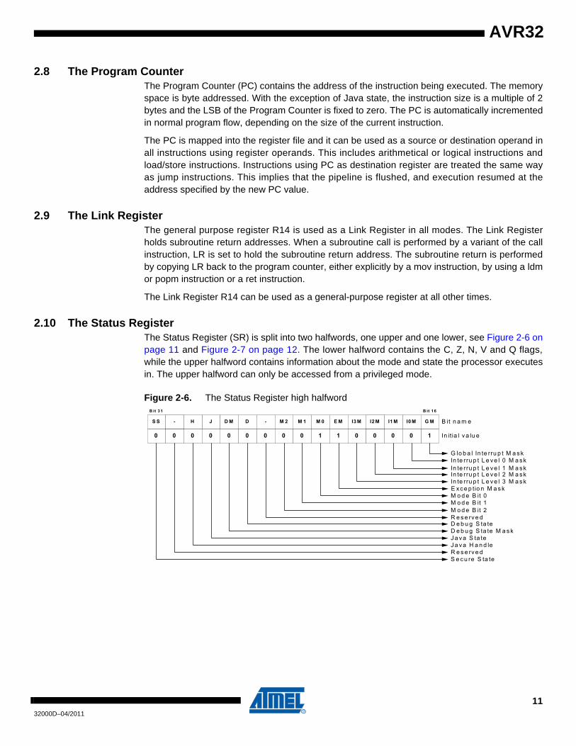
2.10 The Status RegisterThe Status Register (SR) is split into two halfwords, one upper and one lower, see Figure 2-6 onpage 11 and Figure 2-7 on page 12. The lower halfword contains the C, Z, N, V and Q flags,while the upper halfword contains information about the mode and state the processor executesin. The upper halfword can only be accessed from a privileged mode.
Figure 2-6. The Status Register high halfwordB it 3 1
0 0 0
B it 1 6
In te rru p t L e v e l 0 M a s kIn te rru p t L e v e l 1 M a s k
In te rru p t L e v e l 3 M a s kIn te rru p t L e v e l 2 M a s k
10 0 0 0 1 1 0 0 0 00 0
S e c u re S ta te
F E I0 M G MM 1J D M 0 E M I2 MD M - M 2L C1S S
In it ia l v a lu e
B it n a m eI1 M
M o d e B it 0M o d e B it 1
H
M o d e B it 2R e s e rv e dD e b u g S ta te
- I3 M
J a v a S ta te
E x c e p tio n M a s k
G lo b a l In te rru p t M a s k
D e b u g S ta te M a s k
J a v a H a n d leR e s e rv e d
1132000D–04/2011

Figure 2-7. The Status Register low halfword
SS - Secure StateThis bit is indicates if the processor is executing in the secure state. For more details, see chap-ter 4. The bit is initialized in an IMPLEMENTATION DEFINED way at reset.
H - Java HandleThis bit is included to support different heap types in the Java Virtual Machine. For more details,see chapter 3. The bit is cleared at reset.
J - Java StateThe processor is in Java state when this bit is set. The incoming instruction stream will bedecoded as a stream of Java bytecodes, not RISC opcodes. The bit is cleared at reset. This bitshould not be modified by the user as undefined behaviour may result.
DM - Debug State MaskIf this bit is set, the Debug State is masked and cannot be entered. The bit is cleared at reset,and can both be read and written by software.
D - Debug StateThe processor is in debug state when this bit is set. The bit is cleared at reset and should only bemodified by debug hardware, the breakpoint instruction or the retd instruction. Undefined behav-iour may result if the user tries to modify this bit manually.
M2, M1, M0 - Execution ModeThese bits show the active execution mode. The settings for the different modes are shown inTable 2-5 on page 13. M2 and M1 are cleared by reset while M0 is set so that the processor is insupervisor mode after reset. These bits are modified by hardware, or execution of certaininstructions like scall, rets and rete. Undefined behaviour may result if the user tries to modifythese bits manually.
B it 1 5 B it 0
R e s e rv e d
C a rryZ e roS ig n
0 0 0 00000000000
- - --TR B it n a m e
In it ia l v a lu e0 0
L Q V N Z C-
O v e r f lo wS a tu ra t io n
- - -
L o c k
R e g is te r R e m a p E n a b leS c ra tc h
1232000D–04/2011
AVR32

AVR32
EM - Exception maskWhen this bit is set, exceptions are masked. Exceptions are enabled otherwise. The bit is auto-matically set when exception processing is initiated or Debug Mode is entered. Software mayclear this bit after performing the necessary measures if nested exceptions should be supported.This bit is set at reset.
I3M - Interrupt level 3 maskWhen this bit is set, level 3 interrupts are masked. If I3M and GM are cleared, INT3 interruptsare enabled. The bit is automatically set when INT3 processing is initiated. Software may clearthis bit after performing the necessary measures if nested INT3s should be supported. This bit iscleared at reset.
I2M - Interrupt level 2 maskWhen this bit is set, level 2 interrupts are masked. If I2M and GM are cleared, INT2 interruptsare enabled. The bit is automatically set when INT3 or INT2 processing is initiated. Softwaremay clear this bit after performing the necessary measures if nested INT2s should be supported.This bit is cleared at reset.
I1M - Interrupt level 1 maskWhen this bit is set, level 1 interrupts are masked. If I1M and GM are cleared, INT1 interruptsare enabled. The bit is automatically set when INT3, INT2 or INT1 processing is initiated. Soft-ware may clear this bit after performing the necessary measures if nested INT1s should besupported. This bit is cleared at reset.
I0M - Interrupt level 0 maskWhen this bit is set, level 0 interrupts are masked. If I0M and GM are cleared, INT0 interruptsare enabled. The bit is automatically set when INT3, INT2, INT1 or INT0 processing is initiated.Software may clear this bit after performing the necessary measures if nested INT0s should besupported. This bit is cleared at reset.
GM - Global Interrupt MaskWhen this bit is set, all interrupts are disabled. This bit overrides I0M, I1M, I2M and I3M. The bitis automatically set when exception processing is initiated, Debug Mode is entered, or a Javatrap is taken. This bit is automatically cleared when returning from a Java trap. This bit is setafter reset.
Table 2-5. Mode bit settings
M2 M1 M0 Mode
1 1 1 Non Maskable Interrupt
1 1 0 Exception
1 0 1 Interrupt level 3
1 0 0 Interrupt level 2
0 1 1 Interrupt level 1
0 1 0 Interrupt level 0
0 0 1 Supervisor
0 0 0 Application
1332000D–04/2011
R - Java register remapWhen this bit is set, the addresses of the registers in the register file is dynamically changed.This allows efficient use of the register file registers as a stack. For more details, see chapter 3..The R bit is cleared at reset. Undefined behaviour may result if this bit is modified by the user.
T - Scratch bitThis bit is not set or cleared implicit by any instruction and the programmer can therefore usethis bit as a custom flag to for example signal events in the program. This bit is cleared at reset.
L - Lock flagUsed by the conditional store instruction. Used to support atomical memory access. Automati-cally cleared by rete. This bit is cleared after reset.
Q - Saturation flagThe saturation flag indicates that a saturating arithmetic operation overflowed. The flag is stickyand once set it has to be manually cleared by a csrf instruction after the desired action has beentaken. See the Instruction set description for details.
V - Overflow flagThe overflow flag indicates that an arithmetic operation overflowed. See the Instruction setdescription for details.
N - Negative flagThe negative flag is modified by arithmetical and logical operations. See the Instruction setdescription for details.
Z - Zero flagThe zero flag indicates a zero result after an arithmetic or logic operation. See the Instruction setdescription for details.
C - Carry flagThe carry flag indicates a carry after an arithmetic or logic operation. See the Instruction setdescription for details.
2.11 System registersThe system registers are placed outside of the virtual memory space, and are only accessibleusing the privileged mfsr and mtsr instructions, see Table 2-7 on page 15. The number of physi-cal locations is IMPLEMENTATION DEFINED, but a maximum of 256 locations can beaddressed with the dedicated instructions. Some of the System Registers are altered automati-cally by hardware.
The reset value of the System Registers are IMPLEMENTATION DEFINED.
1432000D–04/2011
AVR32
AVR32
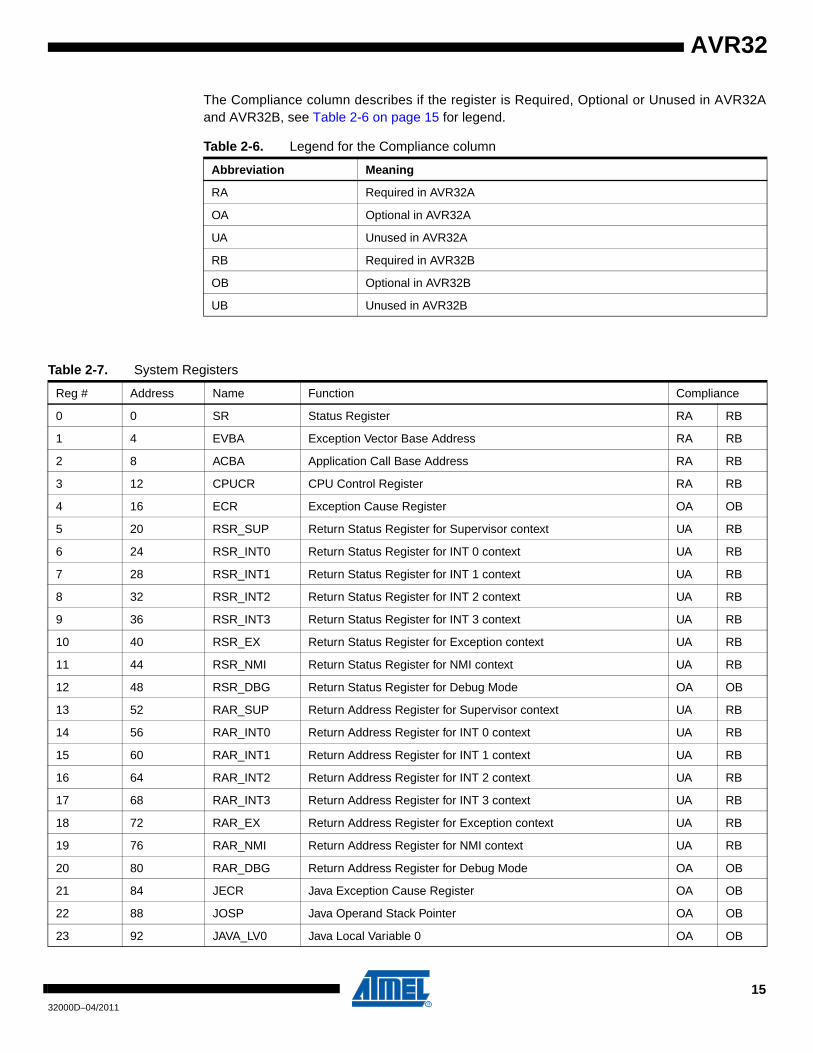
The Compliance column describes if the register is Required, Optional or Unused in AVR32Aand AVR32B, see Table 2-6 on page 15 for legend.
Table 2-6. Legend for the Compliance column
Abbreviation Meaning
RA Required in AVR32A
OA Optional in AVR32A
UA Unused in AVR32A
RB Required in AVR32B
OB Optional in AVR32B
UB Unused in AVR32B
Table 2-7. System Registers
Reg # Address Name Function Compliance
0 0 SR Status Register RA RB
1 4 EVBA Exception Vector Base Address RA RB
2 8 ACBA Application Call Base Address RA RB
3 12 CPUCR CPU Control Register RA RB
4 16 ECR Exception Cause Register OA OB
5 20 RSR_SUP Return Status Register for Supervisor context UA RB
6 24 RSR_INT0 Return Status Register for INT 0 context UA RB
7 28 RSR_INT1 Return Status Register for INT 1 context UA RB
8 32 RSR_INT2 Return Status Register for INT 2 context UA RB
9 36 RSR_INT3 Return Status Register for INT 3 context UA RB
10 40 RSR_EX Return Status Register for Exception context UA RB
11 44 RSR_NMI Return Status Register for NMI context UA RB
12 48 RSR_DBG Return Status Register for Debug Mode OA OB
13 52 RAR_SUP Return Address Register for Supervisor context UA RB
14 56 RAR_INT0 Return Address Register for INT 0 context UA RB
15 60 RAR_INT1 Return Address Register for INT 1 context UA RB
16 64 RAR_INT2 Return Address Register for INT 2 context UA RB
17 68 RAR_INT3 Return Address Register for INT 3 context UA RB
18 72 RAR_EX Return Address Register for Exception context UA RB
19 76 RAR_NMI Return Address Register for NMI context UA RB
20 80 RAR_DBG Return Address Register for Debug Mode OA OB
21 84 JECR Java Exception Cause Register OA OB
22 88 JOSP Java Operand Stack Pointer OA OB
23 92 JAVA_LV0 Java Local Variable 0 OA OB
1532000D–04/2011
24 96 JAVA_LV1 Java Local Variable 1 OA OB
25 100 JAVA_LV2 Java Local Variable 2 OA OB
26 104 JAVA_LV3 Java Local Variable 3 OA OB
27 108 JAVA_LV4 Java Local Variable 4 OA OB
28 112 JAVA_LV5 Java Local Variable 5 OA OB
29 116 JAVA_LV6 Java Local Variable 6 OA OB
30 120 JAVA_LV7 Java Local Variable 7 OA OB
31 124 JTBA Java Trap Base Address OA OB
32 128 JBCR Java Write Barrier Control Register OA OB
33-63 132-252 Reserved Reserved for future use - -
64 256 CONFIG0 Configuration register 0 RA RB
65 260 CONFIG1 Configuration register 1 RA RB
66 264 COUNT Cycle Counter register RA RB
67 268 COMPARE Compare register RA RB
68 272 TLBEHI MMU TLB Entry High OA OB
69 276 TLBELO MMU TLB Entry Low OA OB
70 280 PTBR MMU Page Table Base Register OA OB
71 284 TLBEAR MMU TLB Exception Address Register OA OB
72 288 MMUCR MMU Control Register OA OB
73 292 TLBARLO MMU TLB Accessed Register Low OA OB
74 296 TLBARHI MMU TLB Accessed Register High OA OB
75 300 PCCNT Performance Clock Counter OA OB
76 304 PCNT0 Performance Counter 0 OA OB
77 308 PCNT1 Performance Counter 1 OA OB
78 312 PCCR Performance Counter Control Register OA OB
79 316 BEAR Bus Error Address Register OA OB
80 320 MPUAR0 MPU Address Register region 0 OA OB
81 324 MPUAR1 MPU Address Register region 1 OA OB
82 328 MPUAR2 MPU Address Register region 2 OA OB
83 332 MPUAR3 MPU Address Register region 3 OA OB
84 336 MPUAR4 MPU Address Register region 4 OA OB
85 340 MPUAR5 MPU Address Register region 5 OA OB
86 344 MPUAR6 MPU Address Register region 6 OA OB
87 348 MPUAR7 MPU Address Register region 7 OA OB
88 352 MPUPSR0 MPU Privilege Select Register region 0 OA OB
89 356 MPUPSR1 MPU Privilege Select Register region 1 OA OB
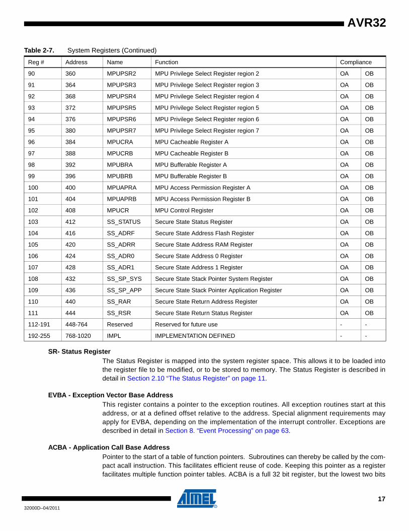
Table 2-7. System Registers (Continued)
Reg # Address Name Function Compliance
1632000D–04/2011
AVR32
AVR32
SR- Status RegisterThe Status Register is mapped into the system register space. This allows it to be loaded intothe register file to be modified, or to be stored to memory. The Status Register is described indetail in Section 2.10 “The Status Register” on page 11.
EVBA - Exception Vector Base AddressThis register contains a pointer to the exception routines. All exception routines start at thisaddress, or at a defined offset relative to the address. Special alignment requirements mayapply for EVBA, depending on the implementation of the interrupt controller. Exceptions aredescribed in detail in Section 8. “Event Processing” on page 63.
ACBA - Application Call Base AddressPointer to the start of a table of function pointers. Subroutines can thereby be called by the com-pact acall instruction. This facilitates efficient reuse of code. Keeping this pointer as a registerfacilitates multiple function pointer tables. ACBA is a full 32 bit register, but the lowest two bits
90 360 MPUPSR2 MPU Privilege Select Register region 2 OA OB
91 364 MPUPSR3 MPU Privilege Select Register region 3 OA OB
92 368 MPUPSR4 MPU Privilege Select Register region 4 OA OB
93 372 MPUPSR5 MPU Privilege Select Register region 5 OA OB
94 376 MPUPSR6 MPU Privilege Select Register region 6 OA OB
95 380 MPUPSR7 MPU Privilege Select Register region 7 OA OB
96 384 MPUCRA MPU Cacheable Register A OA OB
97 388 MPUCRB MPU Cacheable Register B OA OB
98 392 MPUBRA MPU Bufferable Register A OA OB
99 396 MPUBRB MPU Bufferable Register B OA OB
100 400 MPUAPRA MPU Access Permission Register A OA OB
101 404 MPUAPRB MPU Access Permission Register B OA OB
102 408 MPUCR MPU Control Register OA OB
103 412 SS_STATUS Secure State Status Register OA OB
104 416 SS_ADRF Secure State Address Flash Register OA OB
105 420 SS_ADRR Secure State Address RAM Register OA OB
106 424 SS_ADR0 Secure State Address 0 Register OA OB
107 428 SS_ADR1 Secure State Address 1 Register OA OB
108 432 SS_SP_SYS Secure State Stack Pointer System Register OA OB
109 436 SS_SP_APP Secure State Stack Pointer Application Register OA OB
110 440 SS_RAR Secure State Return Address Register OA OB
111 444 SS_RSR Secure State Return Status Register OA OB
112-191 448-764 Reserved Reserved for future use - -
192-255 768-1020 IMPL IMPLEMENTATION DEFINED - -
Table 2-7. System Registers (Continued)
Reg # Address Name Function Compliance
1732000D–04/2011

should be written to zero, making ACBA word aligned. Failing to do so may result in erroneousbehaviour.
CPUCR - CPU Control RegisterRegister controlling the configuration and behaviour of the CPU. The behaviour of this register isIMPLEMENTATION DEFINED. An example of a typical control bit in the CPUCR is an enable bitfor branch prediction.
ECR - Exception Cause RegisterThis register identifies the cause of the most recently executed exception. This information maybe used to handle exceptions more efficiently in certain operating systems. The register isupdated with a value equal to the EVBA offset of the exception, shifted 2 bit positions to theright. Only the 9 lowest bits of the EVBA offset are considered. As an example, an ITLB missjumps to EVBA+0x50. The ECR will then be loaded with 0x50>>2 == 0x14. The ECR register isnot loaded when an scall, Breakpoint or OCD Stop CPU exception is taken. Note that for inter-rupts, the offset is given by the autovector provided by the interrupt controller. The resulting ECRvalue may therefore overlap with an ECR value used by a regular exception. This can beavoided by choosing the autovector offsets so that no such overlaps occur.
RSR_SUP, RSR_INT0, RSR_INT1, RSR_INT2, RSR_INT3, RSR_EX, RSR_NMI - Return Status RegistersIf a request for a mode change, for instance an interrupt request, is accepted when executing ina context C, the Status Register values in context C are automatically stored in the Return Sta-tus Register (RSR) associated with the interrupt context I. When the execution in the interruptstate I is finished and the rets / rete instruction is encountered, the RSR associated with I is cop-ied to SR, and the execution continues in the original context C.
RSR_DBG - Return Status Register for Debug ModeWhen Debug mode is entered, the status register contents of the original mode is automaticallysaved in this register. When the debug routine is finished, the retd instruction copies the con-tents of RSR_DBG into SR.
RAR_SUP, RAR_INT0, RAR_INT1, RAR_INT2, RAR_INT3, RAR_EX, RAR_NMI - Return Address RegistersIf a request for a mode change, for instance an interrupt request, is accepted when executing ina context C, the re-entry address of context C is automatically stored in the Return Address Reg-ister (RAR) associated with the interrupt context I. When the execution in the interrupt state I isfinished and the rets / rete instruction is encountered, a change-of-flow to the address in theRAR associated with I, and the execution continues in the original context C. The calculation ofthe re-entry addresses is described in Section 8. “Event Processing” on page 63.
RAR_DBG - Return Address Register for Debug ModeWhen Debug mode is entered, the Program Counter contents of the original mode is automati-cally saved in this register. When the debug routine is finished, the retd instruction copies thecontents of RAR_DBG into PC.
JECR - Java Exception Cause RegisterThis register contains information needed for Java traps, see AVR32 Java Technical ReferenceManual for details.
JOSP - Java Operand Stack PointerThis register holds the Java Operand Stack Pointer. The register is initialized to 0 at reset.
1832000D–04/2011
AVR32
AVR32
JAVA_LVx - Java Local Variable RegistersThe Java Extension Module uses these registers to store local variables temporary.
JTBA - Java Trap Base AddressThis register contains the base address to the program code for the trapped Java instructions.
JBCR - Java Write Barrier Control RegisterThis register is used by the garbage collector in the Java Virtual Machine.
CONFIG0 / 1 - Configuration Register 0 / 1Used to describe the processor, its configuration and capabilities. The contents and functionalityof these registers is described in detail in Section 2.11.1 “Configuration Registers” on page 21.
COUNT - Cycle Counter RegisterThe COUNT register increments once every clock cycle, regardless of pipeline stalls andflushes. The COUNT register can both be read and written. The count register can be usedtogether with the COMPARE register to create a timer with interrupt functionality. The COUNTregister is written to zero upon reset and compare match. Revision 3 of the AVR32 Architectureallows some implementations to disable this automatic clearing of COUNT upon COMPAREmatch, usually by programming a bit in CPUCR. Refer to the Technical Reference Manual forthe device for details. Incrementation of the COUNT register can not be disabled. The COUNTregister will increment even though a compare interrupt is pending.
COMPARE - Cycle Counter Compare RegisterThe COMPARE register holds a value that the COUNT register is compared against. The COM-PARE register can both be read and written. When the COMPARE and COUNT registers match,a compare interrupt request is generated and COUNT is reset to 0. This interrupt request isrouted out to the interrupt controller, which may forward the request back to the processor as anormal interrupt request at a priority level determined by the interrupt controller. Writing a valueto the COMPARE register clears any pending compare interrupt requests. The compare andexception generation feature is disabled if the COMPARE register contains the value zero. TheCOMPARE register is written to zero upon reset.
TLBEHI - MMU TLB Entry Register High PartUsed to interface the CPU to the TLB. The contents and functionality of the register is describedin detail in Section 5. “Memory Management Unit” on page 35.
TLBELO - MMU TLB Entry Register Low PartUsed to interface the CPU to the TLB. The contents and functionality of the register is describedin detail in Section 5. “Memory Management Unit” on page 35.
PTBR - MMU Page Table Base RegisterContains a pointer to the start of the Page Table. The contents and functionality of the register isdescribed in detail in Section 5. “Memory Management Unit” on page 35.
TLBEAR - MMU TLB Exception Address RegisterContains the virtual address that caused the most recent MMU error. The contents and function-ality of the register is described in detail in Section 5. “Memory Management Unit” on page 35.
1932000D–04/2011
MMUCR - MMU Control RegisterUsed to control the MMU and the TLB. The contents and functionality of the register is describedin detail in Section 5. “Memory Management Unit” on page 35.
TLBARLO / TLBARHI - MMU TLB Accessed Register Low / HighContains the Accessed bits for the TLB. The contents and functionality of the register isdescribed in detail in Section 5. “Memory Management Unit” on page 35.
PCCNT - Performance Clock CounterClock cycle counter for performance counters. The contents and functionality of the register isdescribed in detail in Section 7. “Performance counters” on page 57.
PCNT0 / PCNT1 - Performance Counter 0 / 1Counts the events specified by the Performance Counter Control Register. The contents andfunctionality of the register is described in detail in Section 7. “Performance counters” on page57.
PCCR - Performance Counter Control RegisterControls and configures the setup of the performance counters. The contents and functionalityof the register is described in detail in Section 7. “Performance counters” on page 57.
BEAR - Bus Error Address RegisterPhysical address that caused a Data Bus Error. This register is Read Only. Writes are allowed,but are ignored.
MPUARn - MPU Address Register nRegisters that define the base address and size of the protection regions. Refer to Section 6.“Memory Protection Unit” on page 51 for details.
MPUPSRn - MPU Privilege Select Register nRegisters that define which privilege register set to use for the different subregions in each pro-tection region. Refer to Section 6. “Memory Protection Unit” on page 51 for details.
MPUCRA / MPUCRB - MPU Cacheable Register A / BRegisters that define if the different protection regions are cacheable. Refer to Section 6. “Mem-ory Protection Unit” on page 51 for details.
MPUBRA / MPUBRB - MPU Bufferable Register A / BRegisters that define if the different protection regions are bufferable. Refer to Section 6. “Mem-ory Protection Unit” on page 51 for details.
MPUAPRA / MPUAPRB - MPU Access Permission Register A / BRegisters that define the access permissions for the different protection regions. Refer to Sec-tion 6. “Memory Protection Unit” on page 51 for details.
MPUCR - MPU Control RegisterRegister that control the operation of the MPU. Refer to Section 6. “Memory Protection Unit” onpage 51 for details.
2032000D–04/2011
AVR32

AVR32
SS_STATUS - Secure State Status RegisterRegister that can be used to pass status or other information from the secure state to the nonse-cure state. Refer to Section 4. “Secure state” on page 31 for details.
SS_ADRF, SS_ADRR, SS_ADR0, SS_ADR1 - Secure State Address RegistersRegisters used to partition memories into a secure and a nonsecure section. Refer to Section 4.“Secure state” on page 31 for details.
SS_SP_SYS, SS_SP_APP - Secure State SP_SYS and SP_APP RegistersRead-only registers containing the SP_SYS and SP_APP values. Refer to Section 4. “Securestate” on page 31 for details.
SS_RAR, SS_RSR - Secure State Return Address and Return Status RegistersContains the address and status register of the sscall instruction that called secure state. Alsoused when returning to nonsecure state with the retss instruction. Refer to Section 4. “Securestate” on page 31 for details.
2.11.1 Configuration RegistersConfiguration registers are used to inform applications and operating systems about the setupand configuration of the processor on which it is running, see Figure 2-8 on page 21. The AVR32implements the following read-only configuration registers.
Figure 2-8. Configuration Registers
Table 2-8 on page 21 shows the CONFIG0 fields.
Table 2-8. CONFIG0 Fields
Name Bit Description
Processor ID 31:24Specifies the type of processor. This allows the application to distinguish between different processor implementations.
RESERVED 23:20 Reserved for future use.
Processor revision 19:16 Specifies the revision of the processor implementation.
Processor ID AT
092431
CONFIG0
7 6Processor Revision AR MMUT
23 16 15 13 12 10
S
IMMU SZ ISET
2631
CONFIG1
ILSZ
25 20 19 1516 12
DMMU SZ IASS
13
DSET DLSZ
10 9 6 5
DASS
3
P OF
5
0
J
4
2
3 2
D R
1
-
1920
2132000D–04/2011
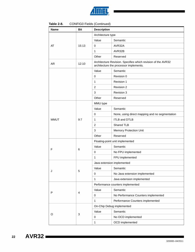
AT 15:13
Architecture type
Value Semantic
0 AVR32A
1 AVR32B
Other Reserved
AR 12:10Architecture Revision. Specifies which revision of the AVR32 architecture the processor implements.
Value Semantic
0 Revision 0
1 Revision 1
2 Revision 2
3 Revision 3
Other Reserved
MMUT 9:7
MMU type
Value Semantic
0 None, using direct mapping and no segmentation
1 ITLB and DTLB
2 Shared TLB
3 Memory Protection Unit
Other Reserved
F 6
Floating-point unit implemented
Value Semantic
0 No FPU implemented
1 FPU implemented
J 5
Java extension implemented
Value Semantic
0 No Java extension implemented
1 Java extension implemented
P 4
Performance counters implemented
Value Semantic
0 No Performance Counters implemented
1 Performance Counters implemented
O 3
On-Chip Debug implemented
Value Semantic
0 No OCD implemented
1 OCD implemented
Table 2-8. CONFIG0 Fields (Continued)
Name Bit Description
2232000D–04/2011
AVR32
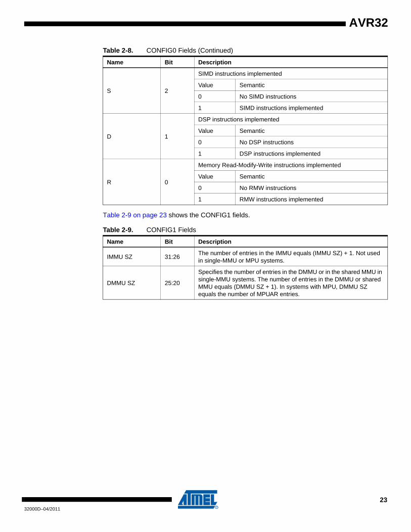
AVR32
Table 2-9 on page 23 shows the CONFIG1 fields.
S 2
SIMD instructions implemented
Value Semantic
0 No SIMD instructions
1 SIMD instructions implemented
D 1
DSP instructions implemented
Value Semantic
0 No DSP instructions
1 DSP instructions implemented
R 0
Memory Read-Modify-Write instructions implemented
Value Semantic
0 No RMW instructions
1 RMW instructions implemented
Table 2-9. CONFIG1 Fields
Name Bit Description
IMMU SZ 31:26The number of entries in the IMMU equals (IMMU SZ) + 1. Not used in single-MMU or MPU systems.
DMMU SZ 25:20
Specifies the number of entries in the DMMU or in the shared MMU in single-MMU systems. The number of entries in the DMMU or shared MMU equals (DMMU SZ + 1). In systems with MPU, DMMU SZ equals the number of MPUAR entries.
Table 2-8. CONFIG0 Fields (Continued)
Name Bit Description
2332000D–04/2011
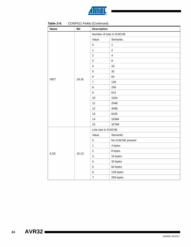
ISET 19:16
Number of sets in ICACHE
Value Semantic
0 1
1 2
2 4
3 8
4 16
5 32
6 64
7 128
8 256
9 512
10 1024
11 2048
12 4096
13 8192
14 16384
15 32768
ILSZ 15:13
Line size in ICACHE
Value Semantic
0 No ICACHE present
1 4 bytes
2 8 bytes
3 16 bytes
4 32 bytes
5 64 bytes
6 128 bytes
7 256 bytes
Table 2-9. CONFIG1 Fields (Continued)
Name Bit Description
2432000D–04/2011
AVR32
AVR32
IASS 12:10
Associativity of ICACHE
Value Semantic
0 Direct mapped
1 2-way
2 4-way
3 8-way
4 16-way
5 32-way
6 64-way
7 128-way
DSET 9:6
Number of sets in DCACHE
Value Semantic
0 1
1 2
2 4
3 8
4 16
5 32
6 64
7 128
8 256
9 512
10 1024
11 2048
12 4096
13 8192
14 16384
15 32768
Table 2-9. CONFIG1 Fields (Continued)
Name Bit Description
2532000D–04/2011
2.12 Recommended Call ConventionThe compiler vendor is free to define a call convention, but seen from a hardware point of view,there are some recommendations on how the call convention should be defined.
Register R12 is intended as return value register in connection with function calls. Some instruc-tions will use this register implicitly. For instance, the conditional ret instruction will move itsargument into R12.
DLSZ 5:3
Line size in DCACHE
Value Semantic
0 No DCACHE present
1 4 bytes
2 8 bytes
3 16 bytes
4 32 bytes
5 64 bytes
6 128 bytes
7 256 bytes
DASS 2:0
Associativity of DCACHE
Value Semantic
0 Direct mapped
1 2-way
2 4-way
3 8-way
4 16-way
5 32-way
6 64-way
7 128-way
Table 2-9. CONFIG1 Fields (Continued)
Name Bit Description
2632000D–04/2011
AVR32

AVR32
3. Java Extension ModuleThe AVR32 architecture can optionally support execution of Java bytecodes by including a JavaExtension Module (JEM). This support is included with minimal hardware overhead.
Comparing Java bytecode instructions with native AVR32 instructions, we see that a large partof the instructions overlap as illustrated in Figure 3-1 on page 27. The idea is thus to reuse thehardware resources by adding a separate Java instruction decoder and control module that exe-cutes in Java state. The processor keeps track of its execution state through the status registerand changes execution mode seamlessly.
In a larger runtime system, an operating system keeps track of and dispatches different pro-cesses. A Java program will typically be one, or several, of these processes.
The Java state is not to be confused with the security modes “system” and “application”, as theJEM can execute in both modes. When the processor switches instruction decoder and entersJava state, it does not affect the security level set by the system. A Java program could also beexecuted from the different interrupt levels without interfering with the mode settings of the pro-cessor, although it is not recommended that interrupt routines are written in Java due to latency.
The Java binary instructions are called bytecodes. These bytecodes are one or more bytes long.A bytecode consists of an opcode and optional arguments. The bytecodes include some instruc-tions with a high semantic content. In order to reduce the hardware overhead, these instructionsare trapped and executed as small RISC programs. These programs are stored in the programmemory and can be changed by the programmer (part of the Java VM implementation). Thisgives full flexibility with regards to future extensions of the Java instruction set. Performance isensured through an efficient trapping mechanism and “Java tailored” RISC instructions.
Figure 3-1. A large part of the instruction set is shared between the AVR RISC and the Java Virtual Machine. The Java instruction set includes instructions with high semantic contents while the AVR RISC instruction set complements Java’s set with tradi-tional hardware near RISC instructions
3.1 The AVR32 Java Virtual MachineThe AVR32 Java Virtual machine consists of two parts, the Java Extension Module in hardwareand the AVR32 specific Java Virtual Machine software, see Figure 3-2 on page 28. Together,the two modules comply with the Java Virtual Machine specification.
High level instructions Low level instructions
� Java additions
AVR RISC additions
Java AVR
Common
2732000D–04/2011

The AVR32 Java Virtual Machine software loads and controls the execution of the Java classes.The bytecodes are executed in hardware, except for some instructions, for example the instruc-tions that create or manipulate objects. These are trapped and executed in software within theJava Virtual Machine.
Figure 3-2. Overview of the AVR32 Java Virtual Machine and the Java Extension Module. The grey area represent the software parts of the virtual machine, while the white box to the right represents the hardware module.
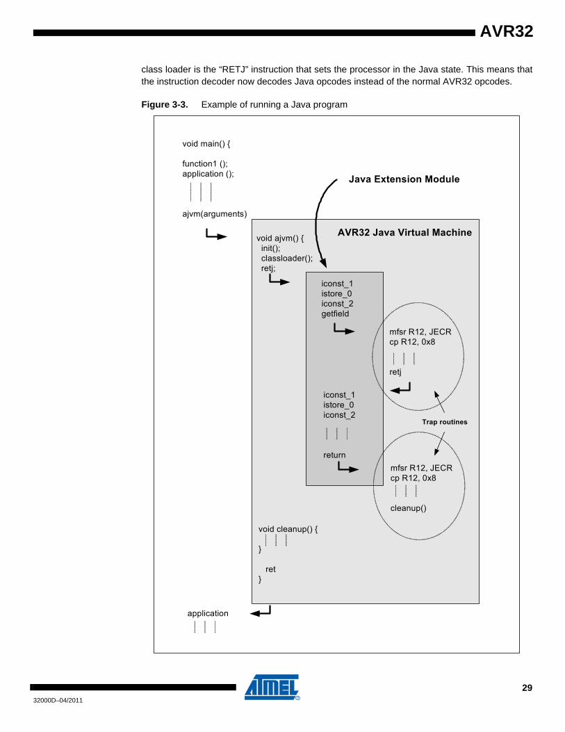
Figure 3-3 on page 29 shows one example on how a Java program is executed. The processorboots in AVR32 (RISC) state and it executes applications as a normal RISC processor. Toinvoke a Java program, the Java Virtual Machine is called like any other application. The JavaVirtual Machine will execute an init routine followed by a class loader that parses the class andinitializes all registers necessary to start executing the Java program. The last instruction in the
Header Data
Class Variables Attributes
Methods Meta Data
Constant Pool
Garbage Collector
Stack PC, SP
Local Variables Const. Pool Pointer
Trapped Object
Bytecodes
Scheduler
AVR32 Java Extension
Module
Other Trapped
Bytecodes
AVR32 Java Virtual Machine
Heap
Objects
Method Area
Classes
Threads
Frames
2832000D–04/2011
AVR32
AVR32
class loader is the “RETJ” instruction that sets the processor in the Java state. This means thatthe instruction decoder now decodes Java opcodes instead of the normal AVR32 opcodes.
Figure 3-3. Example of running a Java program
void ajvm() { init(); classloader(); retj;
iconst_1istore_0iconst_2getfield
iconst_1istore_0iconst_2
return
void cleanup() {
}
ret }
Java Extension Module
AVR32 Java Virtual Machine
mfsr R12, JECRcp R12, 0x8
cleanup()
application
mfsr R12, JECRcp R12, 0x8
retj
Trap routines
void main() {
function1 ();application ();
ajvm(arguments)
2932000D–04/2011
During execution of the Java program, the Java Extension Module will encounter some byte-codes that are not supported in hardware. The instruction decoder will automatically recognizethese bytecodes and switch the processor back into RISC state and at the same time jump to apredefined location where it will execute a software routine that performs the semantic of thetrapped bytecode. When finished, the routine ends with a “RETJ” instruction. This instruction willmake the AVR32 core return to Java state and the Java program will continue at the correctlocation.
Detailed technical information about the Java Extension module is available in a separate JavaTechnical Reference document.
3032000D–04/2011
AVR32
AVR32
4. Secure stateRevision 3 of the AVR32 architecture introduces a secure execution state. This state is intendedto allow execution of a proprietary secret code alongside code of unknown origin and intent onthe same processor. For example, a company with a proprietary algorithm can program thisalgorithm into the secure memory sections of the device, and resell the device with the pro-grammed algorithm to an end customer. The end customer will not be able to read or modify thepreprogrammed code in any way. Examples of such preprogrammed code can be multimediacodecs, digital signal processing algorithms or telecom software stacks. Whereas previousapproaches to this problem required the proprietary code and the end user application to exe-cute on separate devices, the secure state allows integration of the two codes on the samedevice, saving cost and increasing performance since inter-IC communication is no longerrequired.
In order to keep the proprietary code secret, this code will execute in a “secure world”. The enduser application will execute in a “nonsecure world”. Code in the nonsecure world can requestservices from the secure world by executing a special instruction, sscall. This instruction is exe-cuted in the context of an API specified by the provider of the proprietary code. The sscallinstruction can be associated with arguments passed in registers or memory, and after execu-tion of the requested algorithm, the secure world returns results to the requesting nonsecureapplication in registers or in memory.
Hardware is implemented to divide the memory resources into two sections, one secure and onenon-secure section. The secure section of the memories can only be accessed (read, written orexecuted) from code running in the secure world. The nonsecure section of the memories canbe read, written or executed from the nonsecure world, and read or written from the secureworld.
The customer can choose if his application will enable the secure state support or not. AnIMPLEMENTATION DEFINED mechanism, usually a Flash fuse, is used to enable or disablesecure state support. If this mechanism is programmed so as to disable the secure state, thesystem will boot in nonsecure world, and its behavior will be identical to previous devices imple-menting older revisions of the AVR32 architecture. If the system is set up to enable secure statesupport, the system will boot in the secure state. This allows configuration and startup of thesecure world application before execution is passed to the nonsecure world.
4.1 Mechanisms implementing the Secure StateThe following architectural mechanisms are used to implement the secure state:
• The sscall and retss instructions are used for passing between the secure and nonsecure worlds.
• The secure world has a dedicated stack pointer, SP_SEC, which is automatically banked into the register file whenever executing in the secure world.
• The SS bit is set in the status register whenever the system is in the secure state. Only sscall and retss can alter this bit.
• Interrupts and exceptions have special handler addresses used when receiving interrupts or exceptions in the secure world. This allows executing the interrupt or exception handler in the secure world, or jumping back into the nonsecure world to execute the handler there.
• A set of secure system registers are used to configure the secure world behavior, and to aid in communication between the secure and nonsecure worlds. These registers can be written when in the secure world, but only read when in the nonsecure world.
3132000D–04/2011
• When trying to access secure world memories from the nonsecure world, a bus error exception will be raised, and the access will be aborted. Writes to secure system registers from within the nonsecure world will simply be disregarded without any error indication.
• The On-Chip Debug (OCD) system is modified to prevent any leak of proprietary code or data to the nonsecure world. This prevents hacking through the use of the OCD system.
4.2 Secure state programming modelThe programming model in the secure state is similar to in normal RISC state, except thatSP_SEC has been banked in, and the secure system registers are available in all privilegedmodes.
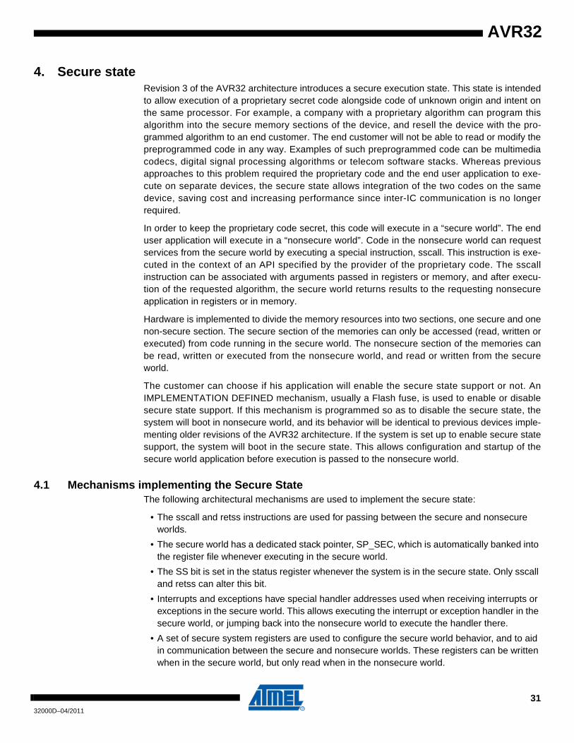
Figure 4-1. Register File in AVR32A with secure contextApplication
Bit 0
Supervisor
Bit 31
PC
SR
INT0PC
FINTPCINT1PC
SMPC
R7
R5R6
R4R3
R1R2
R0
Bit 0Bit 31
PC
SR
R12
INT0PC
FINTPCINT1PC
SMPC
R7
R5R6
R4
R11
R9R10
R8
R3
R1R2
R0
INT0
SP_APP SP_SYSR12R11
R9R10
R8
Exception NMIINT1 INT2 INT3
LRLR
Bit 0Bit 31
PC
SR
R12
INT0PC
FINTPCINT1PC
SMPC
R7
R5R6
R4
R11
R9R10
R8
R3
R1R2
R0
SP_SYSLR
Bit 0Bit 31
PC
SR
R12
INT0PC
FINTPCINT1PC
SMPC
R7
R5R6
R4
R11
R9R10
R8
R3
R1R2
R0
SP_SYSLR
Bit 0Bit 31
PC
SR
R12
INT0PC
FINTPCINT1PC
SMPC
R7
R5R6
R4
R11
R9R10
R8
R3
R1R2
R0
SP_SYSLR
Bit 0Bit 31
PC
SR
R12
INT0PC
FINTPCINT1PC
SMPC
R7
R5R6
R4
R11
R9R10
R8
R3
R1R2
R0
SP_SYSLR
Bit 0Bit 31
PC
SR
R12
INT0PC
FINTPCINT1PC
SMPC
R7
R5R6
R4
R11
R9R10
R8
R3
R1R2
R0
SP_SYSLR
Bit 0Bit 31
PC
SR
R12
INT0PC
FINTPCINT1PC
SMPC
R7
R5R6
R4
R11
R9R10
R8
R3
R1R2
R0
SP_SYSLR
Secure
Bit 0Bit 31
PC
SR
R12
INT0PC
FINTPCINT1PC
SMPC
R7
R5R6
R4
R11
R9R10
R8
R3
R1R2
R0
SP_SECLR
SS_STATUSSS_ADRFSS_ADRRSS_ADR0SS_ADR1
SS_SP_SYSSS_SP_APP
SS_RARSS_RSR
3232000D–04/2011
AVR32
AVR32
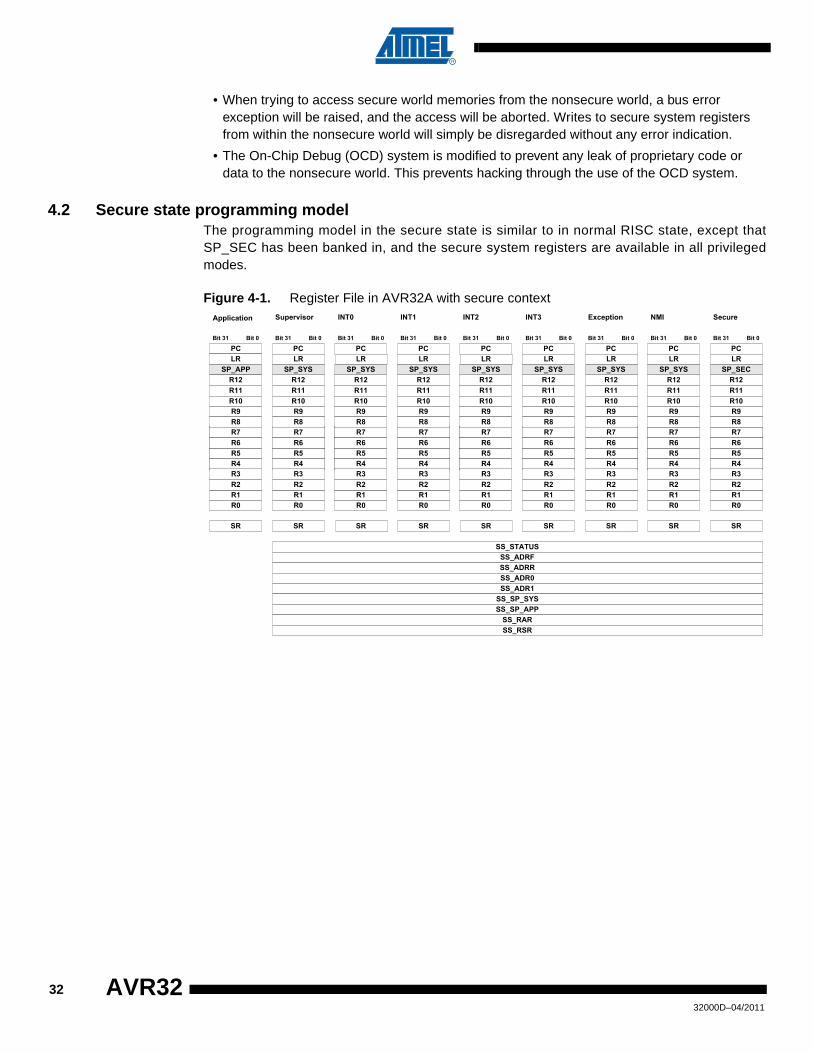
Figure 4-2. Register File in AVR32B with secure context
4.3 Details on Secure State implementationRefer to the Technical Reference manual for the CPU core you are using for details on theSecure State implementation.
Application
Bit 0
Supervisor
Bit 31
PC
SR
INT0PC
FINTPCINT1PC
SMPC
R7
R5R6
R4R3
R1R2
R0
Bit 0Bit 31
PC
SR
R12
INT0PC
FINTPCINT1PC
SMPC
R7
R5R6
R4
R11
R9R10
R8
R3
R1R2
R0
INT0
Bit 0Bit 31
PC
RSR_INT0SR
SP_APP SP_SYS SP_SYSR12R11
R9R10
R8banked
registers(implementation
defined)
Bit 0Bit 31
PCLR / LR_INT2
SP_SYS
banked registers
(implementation defined)
RSR_INT2SR
Bit 0Bit 31
PC
RSR_INT3
LR / LR_INT3
SR
SP_SYS
banked registers
(implementation defined)
Bit 0Bit 31
PC
SR
SP_SYS
banked registers
(implementation defined)
RSR_INT1
Exception
Bit 0Bit 31
PC
SR
R12
INT0PC
FINTPCINT1PC
SMPC
R7
R5R6
R4
R11
R9R10
R8
R3
R1R2
R0
SP_SYSLR
RSR_EX
NMI
Bit 0Bit 31
PC
SR
R12
INT0PC
FINTPCINT1PC
SMPC
R7
R5R6
R4
R11
R9R10
R8
R3
R1R2
R0
SP_SYSLR
RSR_NMI
INT1 INT2 INT3
LRLR
RSR_SUP
LR / LR_INT0 LR / LR_INT1
RAR_INT0 RAR_INT2 RAR_INT3RAR_INT1 RAR_EX RAR_NMIRAR_SUP
SS_STATUSSS_ADRFSS_ADRRSS_ADR0SS_ADR1
SS_SP_SYSSS_SP_APP
SS_RARSS_RSR
Secure
Bit 0Bit 31
PC
SR
R12
INT0PC
FINTPCINT1PC
SMPC
R7
R5R6
R4
R11
R9R10
R8
R3
R1R2
R0
SP_SECLR
SS_RARSS_RSR
3332000D–04/2011

3432000D–04/2011
AVR32
AVR32
5. Memory Management UnitThe AVR32 architecture defines an optional Memory Management Unit (MMU). This allows effi-cient implementation of virtual memory and large memory spaces. Virtual memory simplifiesexecution of multiple processes and allows allocation of privileges to different sections of thememory space.
5.1 Memory map in systems with MMUThe AVR32 architecture specifies a 32-bit virtual memory space. This virtual space is mappedinto a 32-bit physical space by a MMU. It should also be noted that not all implementations willuse caches. The cacheability information specified in the figure will therefore not apply for allimplementations. Refer to the implementation-specific Hardware Manual for details.
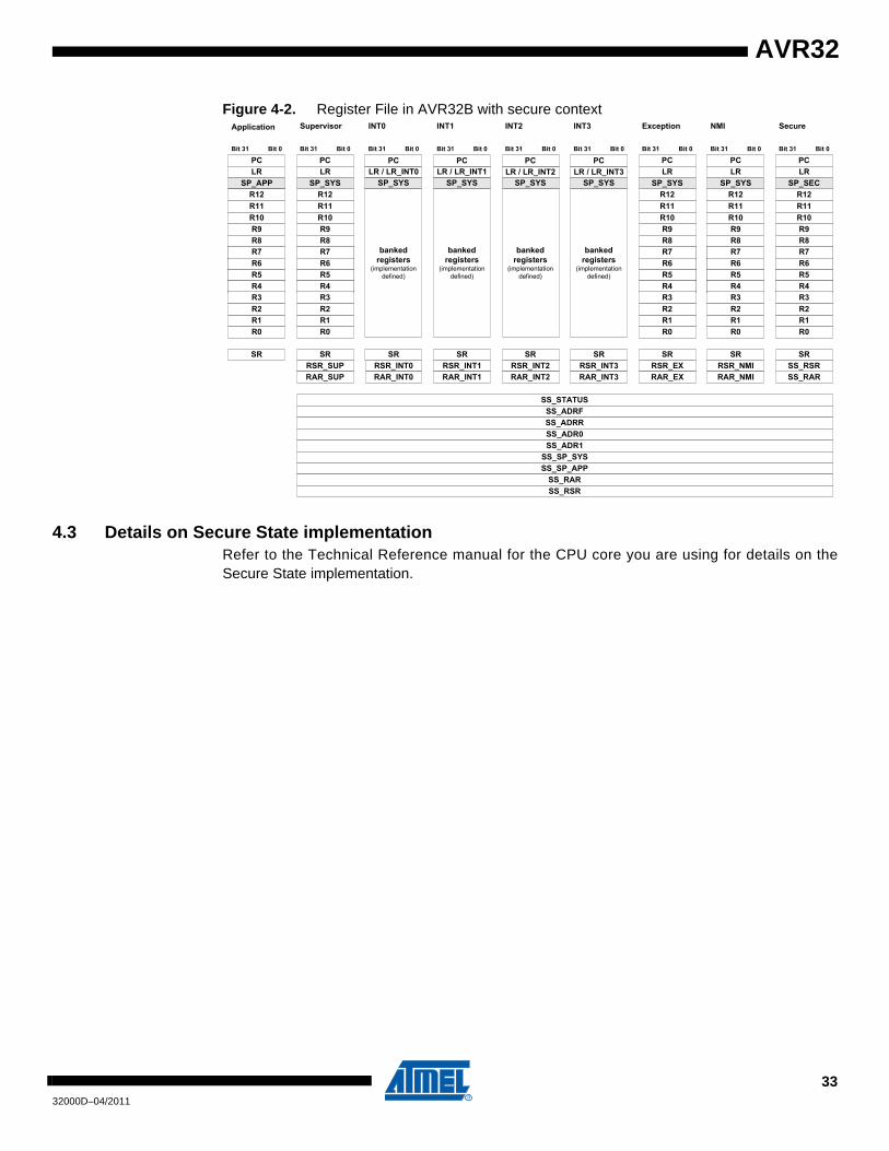
The virtual memory map is specified in Figure 5-1.
Figure 5-1. The AVR32 virtual memory space
The memory map has six different segments, named P0 through P4, and U0. The P-segmentsare accessible in the privileged modes, while the U-segment is accessible in the unprivilegedmode.
Both the P1 and P2 segments are default segment translated to the physical address range0x00000000 to 0x1FFFFFFF. The mapping between virtual addresses and physical addressesis therefore implemented by clearing of MSBs in the virtual address. The difference between P1and P2 is that P1 may be cached, depending on the cache configuration, while P2 is alwaysuncached. Because P1 and P2 are segment translated and not page translated, code for initial-ization of MMUs and exception vectors are located in these segments. P1, being cacheable,may offer higher performance than P2.
2GB translated spaceCacheable
512MB system space, non-cacheable
512MB translated space, cacheable
512MB non-translated space, non-cacheable
512MB non-translated space, cacheable
Unaccessible spaceAccess error
2GB translated spaceCacheable
0x00000000
0x80000000
0xA0000000
0xC0000000
0xE0000000
0xFFFFFFFF
Privileged Modes Unprivileged Mode
0x00000000
0x80000000
0xFFFFFFFF
P0
P1
P2
P3
P4
U0
3532000D–04/2011
The P3 space is also by default segment translated to the physical address range 0x00000000to 0x1FFFFFFF. By enabling and setting up the MMU, the P3 space becomes page translated.Page translation will override segment translation.
The P4 space is intended for memory mapping special system resources like the memory arraysin caches. This segment is non-cacheable, non-translated.
The U0 segment is accessible in the unprivileged user mode. This segment is cacheable andtranslated, depending upon the configuration of the cache and the memory management unit. Ifaccesses to other memory addresses than the ones within U0 is made in application mode, anaccess error exception is issued.
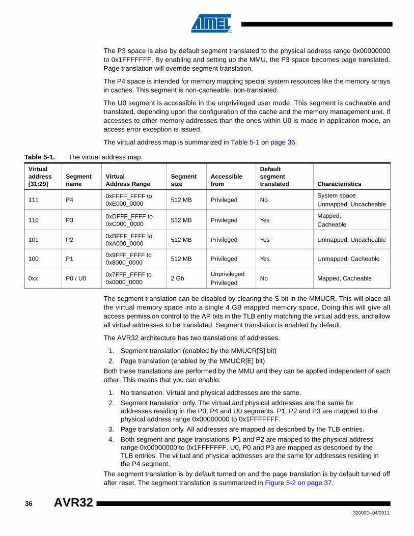
The virtual address map is summarized in Table 5-1 on page 36.
The segment translation can be disabled by clearing the S bit in the MMUCR. This will place allthe virtual memory space into a single 4 GB mapped memory space. Doing this will give allaccess permission control to the AP bits in the TLB entry matching the virtual address, and allowall virtual addresses to be translated. Segment translation is enabled by default.
The AVR32 architecture has two translations of addresses.
1. Segment translation (enabled by the MMUCR[S] bit)
2. Page translation (enabled by the MMUCR[E] bit)
Both these translations are performed by the MMU and they can be applied independent of eachother. This means that you can enable:
1. No translation. Virtual and physical addresses are the same.
2. Segment translation only. The virtual and physical addresses are the same for addresses residing in the P0, P4 and U0 segments. P1, P2 and P3 are mapped to the physical address range 0x00000000 to 0x1FFFFFFF.
3. Page translation only. All addresses are mapped as described by the TLB entries.
4. Both segment and page translations. P1 and P2 are mapped to the physical address range 0x00000000 to 0x1FFFFFFF. U0, P0 and P3 are mapped as described by the TLB entries. The virtual and physical addresses are the same for addresses residing in the P4 segment.
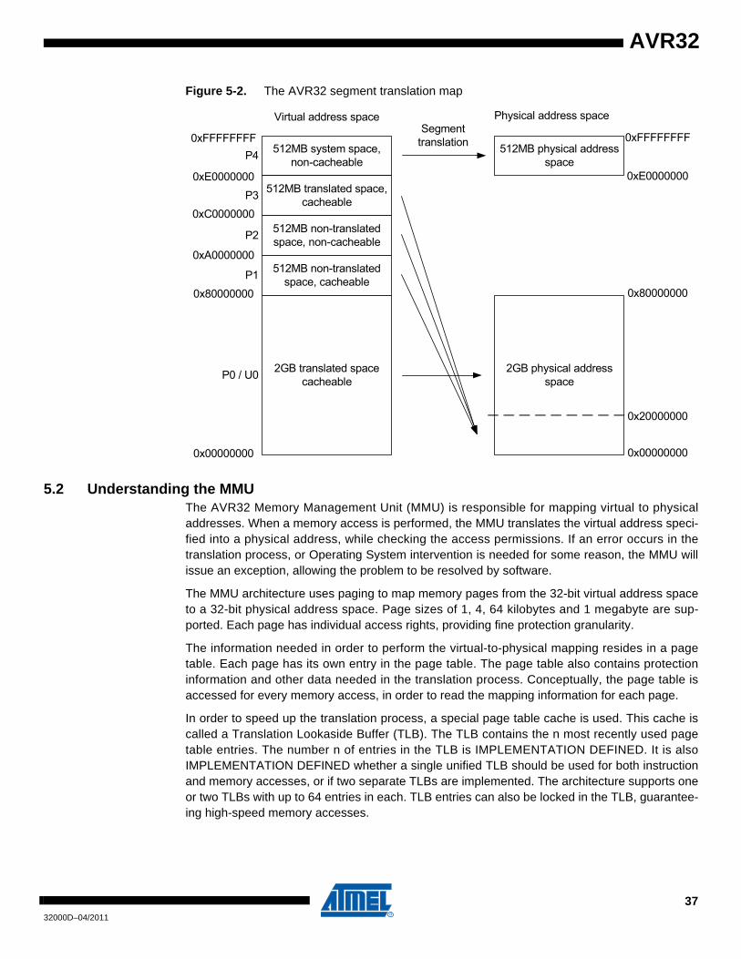
The segment translation is by default turned on and the page translation is by default turned offafter reset. The segment translation is summarized in Figure 5-2 on page 37.
Table 5-1. The virtual address map
Virtualaddress[31:29]
Segmentname
Virtual Address Range
Segmentsize
Accessiblefrom
Defaultsegment translated Characteristics
111 P40xFFFF_FFFF to0xE000_0000
512 MB Privileged NoSystem spaceUnmapped, Uncacheable
110 P30xDFFF_FFFF to0xC000_0000
512 MB Privileged YesMapped,Cacheable
101 P20xBFFF_FFFF to0xA000_0000
512 MB Privileged Yes Unmapped, Uncacheable
100 P10x9FFF_FFFF to0x8000_0000
512 MB Privileged Yes Unmapped, Cacheable
0xx P0 / U00x7FFF_FFFF to0x0000_0000
2 GbUnprivileged
PrivilegedNo Mapped, Cacheable
3632000D–04/2011
AVR32
AVR32
Figure 5-2. The AVR32 segment translation map
5.2 Understanding the MMUThe AVR32 Memory Management Unit (MMU) is responsible for mapping virtual to physicaladdresses. When a memory access is performed, the MMU translates the virtual address speci-fied into a physical address, while checking the access permissions. If an error occurs in thetranslation process, or Operating System intervention is needed for some reason, the MMU willissue an exception, allowing the problem to be resolved by software.
The MMU architecture uses paging to map memory pages from the 32-bit virtual address spaceto a 32-bit physical address space. Page sizes of 1, 4, 64 kilobytes and 1 megabyte are sup-ported. Each page has individual access rights, providing fine protection granularity.
The information needed in order to perform the virtual-to-physical mapping resides in a pagetable. Each page has its own entry in the page table. The page table also contains protectioninformation and other data needed in the translation process. Conceptually, the page table isaccessed for every memory access, in order to read the mapping information for each page.
In order to speed up the translation process, a special page table cache is used. This cache iscalled a Translation Lookaside Buffer (TLB). The TLB contains the n most recently used pagetable entries. The number n of entries in the TLB is IMPLEMENTATION DEFINED. It is alsoIMPLEMENTATION DEFINED whether a single unified TLB should be used for both instructionand memory accesses, or if two separate TLBs are implemented. The architecture supports oneor two TLBs with up to 64 entries in each. TLB entries can also be locked in the TLB, guarantee-ing high-speed memory accesses.
2GB translated spacecacheable
512MB system space, non-cacheable
512MB translated space, cacheable
512MB non-translated space, non-cacheable
512MB non-translated space, cacheable
0x00000000
0x80000000
0xA0000000
0xC0000000
0xE0000000
0xFFFFFFFF
P0 / U0
P1
P2
P3
P4
2GB physical address space
Virtual address space
512MB physical address space
0x00000000
0x80000000
0xE0000000
0xFFFFFFFF
0x20000000
Physical address spaceSegment
translation
3732000D–04/2011

5.2.1 Virtual Memory ModelsThe MMU provides two different virtual memory models, selected by the Mode (M) bit in theMMU Control Register:
• Shared virtual memory, where the same virtual address space is shared between all processes
• Private virtual memory, where each process has its own virtual address space
In shared virtual memory, the virtual address uniquely identifies which physical address it shouldbe mapped to. Two different processes addressing the same virtual address will always accessthe same physical address. In other words, the Virtual Page Number (VPN) section of the virtualaddress uniquely specifies the Physical Frame Number (PFN) section in the physical address.
In private virtual memory, each process has its own virtual memory space. This is implementedby using both the VPN and the Application Space Identifier (ASID) of the current process whensearching the TLB for a match. Each process has a unique ASID. Therefore, two different pro-cesses accessing the same VPN won’t hit the same TLB entry, since their ASID is different.Pages can be shared between processes in private virtual mode by setting the Global (G) bit inthe page table entry. This will disable the ASID check in the TLB search, causing the VPN sec-tion uniquely to identify the PFN for the particular page.
5.2.2 MMU interface registersThe following registers are used to control the MMU, and provide the interface between theMMU and the operating system. Most registers can be altered both by the application software(by writing to them) and by hardware when an exception occurs. All the registers are mappedinto the System Register space, their addresses are presented in Section 2.11 “System regis-ters” on page 14. The MMU interface registers are shown in Figure 5-3.
Figure 5-3. The MMU interface registers
V P N A S ID
G D
071031
TLB E H I
P F N C B
091031
TLB E LO
V
S ZA P W
I
8 7 6 4 3 2 1
P T B R
031
P T B R
T LB E A R
031
TLB E A R
D LA EM
07831
M M U C R
ILA D R PIR P
1
-
213142026 1925
I
3
9 8
N
45
S
T LB A R LO / T LB A R H I
031
TLB A R LO / T LB A R H I
3832000D–04/2011
AVR32

AVR32
5.2.2.1 TLB Entry Register High Part - TLBEHIThe contents of the TLBEHI and TLBELO registers is loaded into the TLB when the tlbw instruc-tion is executed. The TLBEHI register consists of the following fields:
• VPN - Virtual Page Number in the TLB entry. This field contains 22 bits, but the number of bits used depends on the page size. A page size of 1 kB requires 22 bits, while larger page sizes require fewer bits. When preparing to write an entry into the TLB, the virtual page number of the entry to write should be written into VPN. When an MMU-related exception has occurred, the virtual page number of the failing address is written to VPN by hardware.
• V - Valid. Set if the TLB entry is valid, cleared otherwise. This bit is written to 0 by a reset. If an access to a page which is marked as invalid is attempted, an TLB Miss exception is raised. Valid is set automatically by hardware whenever an MMU exception occurs.
• I - Instruction TLB. If set, the current TLBEHI and TLBELO entries should be written into the Instruction TLB. If cleared, the Data or Unified TLB should be addressed. The I bit is set by hardware when an MMU-related exception occurs, indicating whether the error occurred in the ITLB or the UTLB/DTLB.
• ASID - Application Space Identifier. The operating system allocates a unique ASID to each process. This ASID is written into TLBEHI by the OS, and used in the TLB address match if the MMU is running in Private Virtual Memory mode and the G bit of the TLB entry is cleared. ASID is never changed by hardware.
5.2.2.2 TLB Entry Register Low Part - TLBELOThe contents of the TLBEHI and TLBELO registers is loaded into the TLB when the tlbw instruc-tion is executed. None of the fields in TLBELO are altered by hardware. The TLBELO registerconsists of the following fields:
• PFN - Physical Frame Number to which the VPN is mapped. This field contains 22 bits, but the number of bits used depends on the page size. A page size of 1 kB requires 22 bits, while larger page sizes require fewer bits. When preparing to write an entry into the TLB, the physical frame number of the entry to write should be written into PFN.
• C - Cacheable. Set if the page is cacheable, cleared otherwise.
• G - Global bit used in the address comparison in the TLB lookup. If the MMU is operating in the Private Virtual Memory mode and the G bit is set, the ASID won’t be used in the TLB lookup.
• B - Bufferable. Set if the page is bufferable, cleared otherwise.
• AP - Access permissions specifying the privilege requirements to access the page. The following permissions can be set, see Table 5-2 on page 40.
3932000D–04/2011

• SZ - Size of the page. The following page sizes are provided, see Table 5-3:
• D - Dirty bit. Set if the page has been written to, cleared otherwise. If the memory access is a store and the D bit is cleared, an Initial Page Write exception is raised.
• W - Write through. If set, a write-through cache update policy should be used. Write-back should be used otherwise. The bit is ignored if the cache only supports write-through or write-back.
5.2.2.3 Page Table Base Register - PTBRThis register points to the start of the page table structure. The register is not used by hardware,and can only be modified by software. The register is meant to be used by the MMU-relatedexception routines.
5.2.2.4 TLB Exception Address Register - TLBEARThis register contains the virtual address that caused the most recent MMU-related exception.The register is updated by hardware when such an exception occurs.
5.2.2.5 MMU Control Register - MMUCRThe MMUCR controls the operation of the MMU. The MMUCR has the following fields:
• IRP - Instruction TLB Replacement Pointer. Points to the ITLB entry to overwrite when a new entry is loaded by the tlbw instruction. The IRP field may be updated automatically in an IMPLEMENTATION DEFINED manner in order to optimize the replacement algorithm. The IRP field can also be written by software, allowing the exception routine to implement a replacement algorithm in software. The IRP field is 6 bits wide, allowing a maximum of 64
Table 5-2. Access permissions implied by the AP bits
AP Privileged mode Unprivileged mode
000 Read None
001 Read / Execute None
010 Read / Write None
011 Read / Write / Execute None
100 Read Read
101 Read / Execute Read / Execute
110 Read / Write Read / Write
111 Read / Write / Execute Read / Write / Execute
Table 5-3. Page sizes implied by the SZ bits
SZ Page size Bits used in VPN Bits used in PFN
00 1 kB TLBEHI[31:10] TLBELO[31:10]
01 4 kB TLBEHI[31:12] TLBELO[31:12]
10 64 kB TLBEHI[31:16] TLBELO[31:16]
11 1 MB TLBEHI[31:20] TLBELO[31:20]
4032000D–04/2011
AVR32
AVR32
entries in the ITLB. It is IMPLEMENTATION DEFINED whether to use fewer entries. Impementations with a single unified TLB does not use the IRP field.
• ILA - Instruction TLB Lockdown Amount. Specified the number of locked down ITLB entries. All ITLB entries from entry 0 to entry (ILA-1) are locked down. If ILA equals zero, no entries are locked down. Implementations with a single unified TLB does not use the ILA field.
• DRP - Data TLB Replacement Pointer. Points to the DTLB entry to overwrite when a new entry is loaded by the tlbw instruction. The DRP field may be updated automatically in an IMPLEMENTATION DEFINED manner in order to optimize the replacement algorithm. The DRP field can also be written by software, allowing the exception routine to implement a replacement algorithm in software. The DRP field is 6 bits wide, allowing a maximum of 64 entries in the DTLB. It is IMPLEMENTATION DEFINED whether to use fewer entries. Implementations with a single unified TLB use the DRP field to point into the unified TLB.
• DLA - Data TLB Lockdown Amount. Specified the number of locked down DTLB or UTLB entries. All DTLB entries from entry 0 to entry (DLA-1) are locked down. If DLA equals zero, no entries are locked down.
• S - Segmentation Enable. If set, the segmented memory model is used in the translation process. If cleared, the memory is regarded as unsegmented. The S bit is set after reset.
• N - Not Found. Set if the entry searched for by the TLB Search instruction (tlbs) was not found in the TLB.
• I - Invalidate. Writing this bit to one invalidates all TLB entries. The bit is automatically cleared by the MMU when the invalidate operation is finished.
• M - Mode. Selects whether the shared virtual memory mode or the private virtual memory mode should be used. The M bit determines how the TLB address comparison should be performed, see Table 5-4 on page 41.
• E - Enable. If set, the MMU translation is enabled. If cleared, the MMU translation is disabled and the physical address is identical to the virtual address. Access permissions are not checked and no MMU-related exceptions are issued if the MMU is disabled. If the MMU is disabled, the segmented memory model is used.
5.2.2.6 TLB Accessed Register HI / LO - TLBARHI / TLBARLOThe TLBARHI and TLBARLO register form one 64-bit register with 64 1-bit fields. Each of thesefields contain the Accessed bit for the corresponding TLB entry. The I bit in TLBEHI determineswhether the ITLB or DTLB Accessed bits are read. The Accessed bit is 0 if the page has beenaccessed, and 1 if it has not been accessed. Bit 31-0 in TLBARLO correspond to TLB entry 0-31, bit 31-0 in TLBARHI correspond to TLB entry 32-63. If the TLB implementation contains lessthan 64 entries then nonimplemented entries are read as 0.
Note: The contents of TLBARHI/TLBARLO are reversed to let the Count Leading Zero (CLZ)instruction be used directly on the contents of the registers. E.g. if CLZ returns the value four onthe contents of TLBARLO, then item four is the first unused item in the TLB.
Table 5-4. MMU mode implied by the M bit
M Mode
0 Private Virtual Memory
1 Shared Virtual Memory
4132000D–04/2011
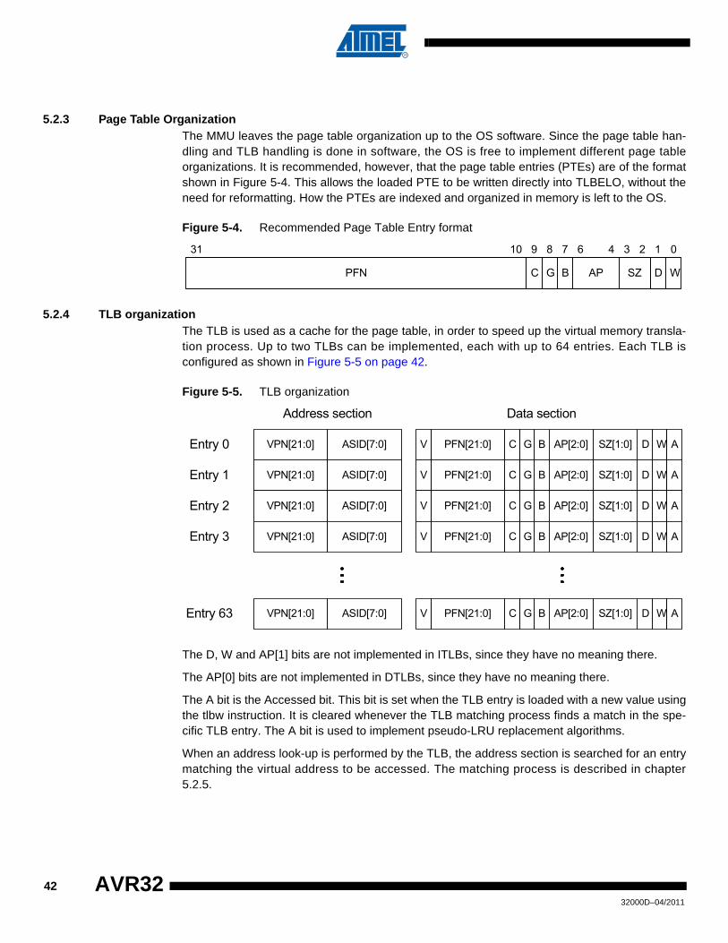
5.2.3 Page Table OrganizationThe MMU leaves the page table organization up to the OS software. Since the page table han-dling and TLB handling is done in software, the OS is free to implement different page tableorganizations. It is recommended, however, that the page table entries (PTEs) are of the formatshown in Figure 5-4. This allows the loaded PTE to be written directly into TLBELO, without theneed for reformatting. How the PTEs are indexed and organized in memory is left to the OS.
Figure 5-4. Recommended Page Table Entry format
5.2.4 TLB organizationThe TLB is used as a cache for the page table, in order to speed up the virtual memory transla-tion process. Up to two TLBs can be implemented, each with up to 64 entries. Each TLB isconfigured as shown in Figure 5-5 on page 42.
Figure 5-5. TLB organization
The D, W and AP[1] bits are not implemented in ITLBs, since they have no meaning there.
The AP[0] bits are not implemented in DTLBs, since they have no meaning there.
The A bit is the Accessed bit. This bit is set when the TLB entry is loaded with a new value usingthe tlbw instruction. It is cleared whenever the TLB matching process finds a match in the spe-cific TLB entry. The A bit is used to implement pseudo-LRU replacement algorithms.
When an address look-up is performed by the TLB, the address section is searched for an entrymatching the virtual address to be accessed. The matching process is described in chapter5.2.5.
G DPFN C B
091031
SZAP W
8 7 6 4 3 2 1
VPN[21:0] ASID[7:0] G DPFN[21:0] C BV AP[2:0] WEntry 0
VPN[21:0] ASID[7:0] G DPFN[21:0] C BV AP[2:0] WEntry 1
VPN[21:0] ASID[7:0] G WPFN[21:0] C BV AP[2:0] DEntry 2
VPN[21:0] ASID[7:0] G WPFN[21:0] C BV AP[2:0] DEntry 3
VPN[21:0] ASID[7:0] G WPFN[21:0] C BV AP[2:0] DEntry 63
Address section Data section
SZ[1:0]
SZ[1:0]
SZ[1:0]
SZ[1:0]
SZ[1:0]
A
A
A
A
A
4232000D–04/2011
AVR32
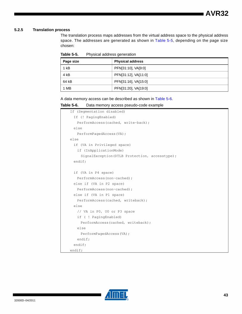
AVR32
5.2.5 Translation processThe translation process maps addresses from the virtual address space to the physical addressspace. The addresses are generated as shown in Table 5-5, depending on the page sizechosen:
A data memory access can be described as shown in Table 5-6.
Table 5-5. Physical address generation
Page size Physical address
1 kB PFN[31:10], VA[9:0]
4 kB PFN[31:12], VA[11:0]
64 kB PFN[31:16], VA[15:0]
1 MB PFN[31:20], VA[19:0]
Table 5-6. Data memory access pseudo-code example
If (Segmentation disabled)
If (! PagingEnabled)
PerformAccess(cached, write-back);
else
PerformPagedAccess(VA);
else
if (VA in Privileged space)
if (InApplicationMode)
SignalException(DTLB Protection, accesstype);
endif;
if (VA in P4 space)
PerformAccess(non-cached);
else if (VA in P2 space)
PerformAccess(non-cached);
else if (VA in P1 space)
PerformAccess(cached, writeback);
else
// VA in P0, U0 or P3 space
if ( ! PagingEnabled)
PerformAccess(cached, writeback);
else
PerformPagedAccess(VA);
endif;
endif;
endif;
4332000D–04/2011
The translation process performed by PerformTranslatedAccess( ) can be described as shownin Table 5-7.Table 5-7. PerformTranslatedAccess( ) pseudo-code example
match ← 0;for (i=0; i<TLBentries; i++)
if ( Compare(TLB[i]VPN, VA, TLB[i]SZ, TLB[i]V) )
// VPN and VA matches for the given page size and entry valid
if ( SharedVirtualMemoryMode or
(PrivateVirtualMemoryMode and ( TLB[i]G or (TLB[i]ASID==TLBEHIASID) ) ) )
if (match == 1)
SignalException(TLBmultipleHit);
else
match ← 1;TLB[i]A ← 1;ptr ← i;// pointer points to the matching TLB entry
endif;
endif;
endfor;
if (match == 0 )
SignalException(DTLBmiss, accesstype);
endif;
if (InApplicationMode)
if (TLB[ptr]AP[2] == 0)
SignalException(DTLBprotection, accesstype);
endif;
endif;
if (accesstype == write)
if (TLB[ptr]AP[1] == 0)
SignalException(DTLBprotection, accesstype);
endif;
if (TLB[ptr]D == 0)
// Initial page write
SignalException(DTLBmodified);
endif;
endif;
if (TLB[ptr]C == 1)
if (TLB[ptr]W == 1)
PerformAccess(cached, write-through);
else
PerformAccess(cached, write-back);
endif;
else
PerformAccess(non-cached);
endif;
4432000D–04/2011
AVR32
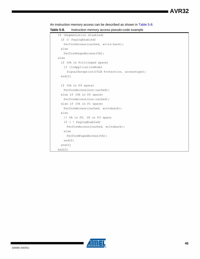
AVR32
An instruction memory access can be described as shown in Table 5-8.
Table 5-8. Instruction memory access pseudo-code example
If (Segmentation disabled)
If (! PagingEnabled)
PerformAccess(cached, write-back);
else
PerformPagedAccess(VA);
else
if (VA in Privileged space)
if (InApplicationMode)
SignalException(ITLB Protection, accesstype);
endif;
if (VA in P4 space)
PerformAccess(non-cached);
else if (VA in P2 space)
PerformAccess(non-cached);
else if (VA in P1 space)
PerformAccess(cached, writeback);
else
// VA in P0, U0 or P3 space
if ( ! PagingEnabled)
PerformAccess(cached, writeback);
else
PerformPagedAccess(VA);
endif;
endif;
endif;
4532000D–04/2011
The translation process performed by PerformTranslatedAccess( ) can be described as asshown in Table 5-9.
Table 5-9. PerformTranslatedAccess( ) pseudo-code example
match ← 0;for (i=0; i<TLBentries; i++)
if ( Compare(TLB[i]VPN, VA, TLB[i]SZ, TLB[i]V) )
// VPN and VA matches for the given page size and entry valid
if ( SharedVirtualMemoryMode or
(PrivateVirtualMemoryMode and ( TLB[i]G or (TLB[i]ASID==TLBEHIASID) ) ) )
if (match == 1)
SignalException(TLBmultipleHit);
else
match ← 1;TLB[i]A ← 1;ptr ← i;// pointer points to the matching TLB entry
endif;
endif;
endfor;
if (match == 0 )
SignalException(ITLBmiss);
endif;
if (InApplicationMode)
if (TLB[ptr]AP[2] == 0)
SignalException(ITLBprotection);
endif;
endif;
if (TLB[ptr]AP[0] == 0)
SignalException(ITLBprotection);
endif;
if (TLB[ptr]C == 1)
PerformAccess(cached);
else
PerformAccess(non-cached);
endif;
4632000D–04/2011
AVR32
AVR32
5.3 Operation of the MMU and MMU exceptionsThe MMU uses both hardware and software mechanisms in order to perform its memory remap-ping operations. The following tasks are performed by hardware:
1. The MMU decodes the virtual address and tries to find a matching entry in the TLB. This entry is used to generate a physical address. If no matching entry is found, a TLB miss exception is issued.
2. The matching entry is used to determine whether the access has the appropriate access rights, cacheability, bufferability and so on. If the access is not permitted, a TLB Protection Violation exception is issued.
3. If any other event arises that requires software intervention, an appropriate exception is issued.
4. If the correct entry was found in the TLB, and the access permissions were not violated, the memory access is performed without any further software intervention.
The following tasks must be performed by software:
1. Setup of the MMU hardware by initializing the MMU-related registers and data struc-tures if needed.
2. Maintenance of the TLB structure. TLB entries are written, invalidated and replaced by means of software. A tlbw instruction is included in the instruction set to support this.
3. The MMU may generate several exceptions. Software exception handlers must be writ-ten in order to service these exceptions.
5.3.1 The tlbw instructionThe tlbw instruction is implemented in order to aid in performing TLB maintenance. The instruc-tion copies the contents of TLBEHI and TLBELO into the TLB entry pointed to by the ITLB orDTLB Replacement Pointers (IRP/DRP) in the MMU Control Register. The TLBEHI[I] bit decidesif the ITLB or the DTLB should be addressed. IRP and DRP may in some implementations beautomatically updated by hardware in order to implement a TLB replacement algorithm in hard-ware. Software may update them before executing tlbw in order to implement a softwarereplacement algorithm.
In some implementations, the TLB data structures may be mapped into the P4 space. In suchimplementations, the TLB data structures may be updated with regular memory accessinstructions.
5.3.2 TLB synonymsImplementations using virtually indexed caches may be subject to cache inconsistencies,depending on the page size used and number of lines in the cache. These inconsistencies mayoccur when multiple virtual addresses are mapped to the same physical address, since a trans-lated part of VPN may be used to index the cache. This implies that the same physical addressmay be mapped to different cache lines, causing cache inconsistency.
Synonym problems can only appear when addressing data residing in a virtually indexed cache.Addressing uncached memory or accessing untranslated memory will never cause synonymproblems.
It is the responsability of the OS to define a policy ensuring that no synonym problems mayarise. No hardware support is provided to avoid TLB synonyms.
4732000D–04/2011
5.3.3 MMU exception handlingThis chapter describes the software actions that must be performed for MMU-related excep-tions. The hardware actions performed by the exceptions are described in detail in Section 8.3.1“Description of events in AVR32A” on page 68.
5.3.3.1 ITLB / DTLB Multiple HitIf multiple matching entries are found when searching the ITLB or DTLB, this exception isissued. This situation is a critical error, since memory consistency can no longer be guaranteed.The exception hardware therefore jumps to the reset vector, where software should execute therequired reset code. This exception is a sign of erroneous code and is not normally generated.
The software handler should perform a normal system restart. However, debugging code maybe inserted in the handler.
5.3.3.2 ITLB / DTLB MissThis exception is issued if no matching entries are found in the TLBs, or when a matching entryis found with the Valid bit cleared. The same actions must be performed for both exceptions, butDTLB entries contains more control bits than the ITLB entries.
1. Examine the TLBEAR and TLBEHI registers in order to identify the page that caused the fault. Use this to index the page table pointed to by PTBR and fetch the desired page table entry.
2. Use the fetched page table entry to update the necessary bits in PTEHI and PTELO. The following bits must be updated, not all bits apply to ITLB entries: V, PFN, C, G, B, AP[2:0], SZ[1:0], W, D.
3. The TLBEHI[I] register is updated by hardware to indicate if it was a ITLB or a DTLB miss. The MMUCR[IRP] and MMUCR[DRP] pointers may be updated in an IMPLE-MENTATION DEFINED way in order to select which TLB entry to replace. The software may override this value by writing a value directly to MMUCR[IRP] or MMUCR[DRP], depending on which TLB to update.
4. Execute the tlbw instruction in order to update the TLB entry.
5. Finish the exception handling and return to the application by executing the rete instruction.
5.3.3.3 ITLB / DTLB Protection ViolationThis exception is issued if the access permision bits in the matching TLB entry does not matchthe privilege level the CPU is currently executing in. The exception is also issued if the MMU isdisabled or absent and non-translated areas are accessed with illegal access rights. The sameactions must be performed for both exceptions, but DTLB entries contains more control bits thanthe ITLB entries.
Software must examine the TLBEAR and TLBEHI registers in order to identify the instructionand process that caused the error. Corrective measures like terminating the process must thenbe performed before returning to normal execution with rete.
4832000D–04/2011
AVR32
AVR32
5.3.3.4 DTLB ModifiedThis exception is issued if a valid memory write operation is performed to a page that has neverbeen written before. This is detected by the Dirty-bit in the matching TLB entry reading zero.
1. Examine the TLBEAR and TLBEHI registers in order to identify the page that caused the fault. Use this to index the page table pointed to by PTBR and fetch the desired page table entry.
2. Set the Dirty bit in the read page table entry and write this entry back to the page table
3. Use the fetched page table entry to update the necessary bits in PTEHI and PTELO. The following bits must be updated: V, PFN, C, G, B, AP[2:0], SZ[1:0], W, D.
4. The TLBEHI[I] register is updated by hardware to indicate that it was a DTLB miss. Ensure that MMUCR[DRP] points to the TLB entry to replace. An entry for the faulting page must already exist in the DTLB, and MMUCR[DRP] must point to this entry, other-wise multiple DTLB hits may occur.
5. Execute the tlbw instruction in order to update the TLB entry.
6. Finish the exception handling and return to the application by executing the rete instruction.
4932000D–04/2011

5032000D–04/2011
AVR32
AVR32
6. Memory Protection UnitThe AVR32 architecture defines an optional Memory Protection Unit (MPU). This is a simpleralternative to a full MMU, while at the same time allowing memory protection. The MPU allowsthe user to divide the memory space into different protection regions. These protection regionshave a user-defined size, and starts at a user-defined address. The different regions can havedifferent cacheability attributes and bufferability attributes. Each region is divided into 16 subre-gions, each of these subregions can have one of two possible sets of access permissions.
The MPU does not perform any address translation.
6.1 Memory map in systems with MPUAn AVR32 implemetation with a MPU has a flat, unsegmented memory space. Access permis-sions are given only by the different protection regions.
6.2 Understanding the MPUThe AVR32 Memory Protection Unit (MPU) is responsible for checking that memory transfershave the correct permissions to complete. If a memory access with unsatisfactory privileges isattempted, an exception is generated and the access is aborted. If an access to a memoryaddress that does not reside in any protection region is attempted, an exception is generatedand the access is aborted.
The user is able to allow different privilege levels to different blocks of memory by configuring aset of registers. Each such block is called a protection region. Each region has a user-program-mable start address and size. The MPU allows the user to program 8 different protectionregions. Each of these regions have 16 sub-regions, which can have different access permis-sions, cacheability and bufferability.
The “DMMU SZ” fields in the CONFIG1 system register identifies the number of implementedprotection regions, and therefore also the number of MPU registers. A system with caches alsohave MPU cacheability and bufferability registers.
A protection region can be from 4 KB to 4 GB in size, and the size must be a power of two. Allregions must have a start address that is aligned to an address corresponding to the size of theregion. If the region has a size of 8 KB, the 13 lowest bits in the start address must be 0. Failingto do so will result in UNDEFINED behaviour. Since each region is divided into 16 sub-regions,each sub-region is 256 B to 256 MB in size.
When an access hits into a memory region set up by the MPU, hardware proceeds to determinewhich subregion the access hits into. This information is used to determine whether the accesspermissions for the subregion are given in MPUAPRA/MPUBRA/MPUCRA or inMPUAPRB/MPUBRB/MPUCRB.
If an access does not hit in any region, the transfer is aborted and an exception is generated.
The MPU is enabled by writing setting the E bit in the MPUCR register. The E bit is cleared afterreset. If the MPU is disabled, all accesses are treated as uncacheable, unbufferable and will notgenerate any access violations. Before setting the E bit, at least one valid protection region mustbe defined.
6.2.1 MPU interface registersThe following registers are used to control the MPU, and provide the interface between the MPUand the operating system, see Figure 6-1 on page 52. All the registers are mapped into the Sys-
5132000D–04/2011
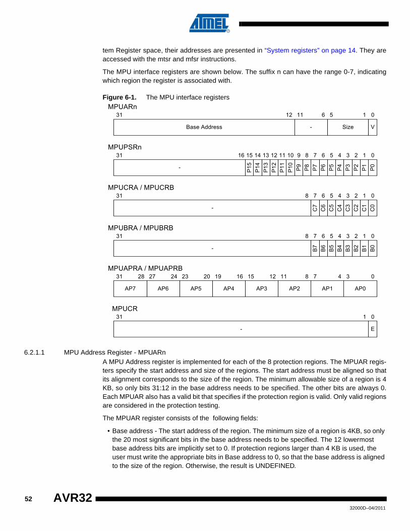
tem Register space, their addresses are presented in “System registers” on page 14. They areaccessed with the mtsr and mfsr instructions.
The MPU interface registers are shown below. The suffix n can have the range 0-7, indicatingwhich region the register is associated with.
Figure 6-1. The MPU interface registers
6.2.1.1 MPU Address Register - MPUARnA MPU Address register is implemented for each of the 8 protection regions. The MPUAR regis-ters specify the start address and size of the regions. The start address must be aligned so thatits alignment corresponds to the size of the region. The minimum allowable size of a region is 4KB, so only bits 31:12 in the base address needs to be specified. The other bits are always 0.Each MPUAR also has a valid bit that specifies if the protection region is valid. Only valid regionsare considered in the protection testing.
The MPUAR register consists of the following fields:
• Base address - The start address of the region. The minimum size of a region is 4KB, so only the 20 most significant bits in the base address needs to be specified. The 12 lowermost base address bits are implicitly set to 0. If protection regions larger than 4 KB is used, the user must write the appropriate bits in Base address to 0, so that the base address is aligned to the size of the region. Otherwise, the result is UNDEFINED.
Base Address Size
051231MPUARn
-
031
-
8 7 6 4 3 2 1
031
031
E
031MPUCR
-
1
11 6
V
1
MPUCRA / MPUCRB5
MPUBRA / MPUBRB
-
8 7 6 4 3 2 15
MPUAPRA / MPUAPRB
AP0AP1AP2AP3AP4AP5AP6AP7
347811121516192023242728
-
31MPUPSRn
P10
P11
P12
P13
P14
P15 P4
P5
P6
P7
P8
P9
P0
P1
P2
P3
08 7 6 4 3 2 15916 15 13 12 11 1014
C4
C5
C6
C7
C0
C1
C2
C3
B4
B5
B6
B7
B0
B1
B2
B3
5232000D–04/2011
AVR32
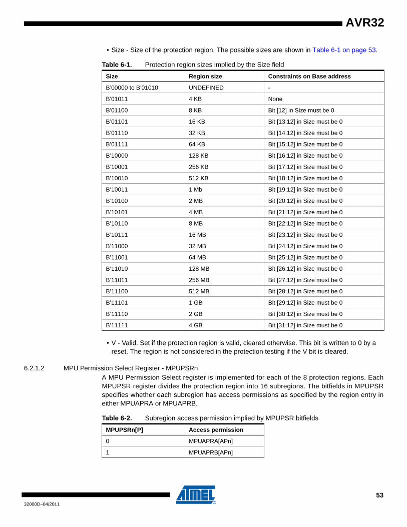
AVR32
• Size - Size of the protection region. The possible sizes are shown in Table 6-1 on page 53.
• V - Valid. Set if the protection region is valid, cleared otherwise. This bit is written to 0 by a reset. The region is not considered in the protection testing if the V bit is cleared.
6.2.1.2 MPU Permission Select Register - MPUPSRnA MPU Permission Select register is implemented for each of the 8 protection regions. EachMPUPSR register divides the protection region into 16 subregions. The bitfields in MPUPSRspecifies whether each subregion has access permissions as specified by the region entry ineither MPUAPRA or MPUAPRB.
Table 6-1. Protection region sizes implied by the Size field
Size Region size Constraints on Base address
B’00000 to B’01010 UNDEFINED -
B’01011 4 KB None
B’01100 8 KB Bit [12] in Size must be 0
B’01101 16 KB Bit [13:12] in Size must be 0
B’01110 32 KB Bit [14:12] in Size must be 0
B’01111 64 KB Bit [15:12] in Size must be 0
B’10000 128 KB Bit [16:12] in Size must be 0
B’10001 256 KB Bit [17:12] in Size must be 0
B’10010 512 KB Bit [18:12] in Size must be 0
B’10011 1 Mb Bit [19:12] in Size must be 0
B’10100 2 MB Bit [20:12] in Size must be 0
B’10101 4 MB Bit [21:12] in Size must be 0
B’10110 8 MB Bit [22:12] in Size must be 0
B’10111 16 MB Bit [23:12] in Size must be 0
B’11000 32 MB Bit [24:12] in Size must be 0
B’11001 64 MB Bit [25:12] in Size must be 0
B’11010 128 MB Bit [26:12] in Size must be 0
B’11011 256 MB Bit [27:12] in Size must be 0
B’11100 512 MB Bit [28:12] in Size must be 0
B’11101 1 GB Bit [29:12] in Size must be 0
B’11110 2 GB Bit [30:12] in Size must be 0
B’11111 4 GB Bit [31:12] in Size must be 0
Table 6-2. Subregion access permission implied by MPUPSR bitfields
MPUPSRn[P] Access permission
0 MPUAPRA[APn]
1 MPUAPRB[APn]
5332000D–04/2011
6.2.1.3 MPU Cacheable Register A / B- MPUCRA / MPUCRBThe MPUCR registers have one bit per region, indicating if the region is cacheable. If the corre-sponding bit is set, the region is cacheable. The register is written to 0 upon reset.
AVR32UC implementations may optionally choose not to implement the MPUCR registers.
6.2.1.4 MPU Bufferable Register A / B- MPUBRA / MPUBRBThe MPUBR registers have one bit per region, indicating if the region is bufferable. If the corre-sponding bit is set, the region is bufferable. The register is written to 0 upon reset.
AVR32UC implementations may optionally choose not to implement the MPUBR registers.
6.2.1.5 MPU Access Permission Register A / B - MPUAPRA / MPUAPRBThe MPUAPR registers indicate the access permissions for each region. The MPUAPR is writ-ten to 0 upon reset. The possible access permissions are shown in Table 6-3 on page 54.
6.2.1.6 MPU Control Register - MPUCRThe MPUCR controls the operation of the MPU. The MPUCR has only one field:
• E - Enable. If set, the MPU address checking is enabled. If cleared, the MPU address checking is disabled and no exceptions will be generated by the MPU.
6.2.2 MPU exception handlingThis chapter describes the exceptions that can be signalled by the MPU.
6.2.2.1 ITLB Protection ViolationAn ITLB protection violation is issued if an instruction fetch violates access permissions. The vio-lating instruction is not executed. The address of the failing instruction is placed on the systemstack.
Table 6-3. Access permissions implied by the APn bits
AP Privileged mode Unprivileged mode
B’0000 Read None
B’0001 Read / Execute None
B’0010 Read / Write None
B’0011 Read / Write / Execute None
B’0100 Read Read
B’0101 Read / Execute Read / Execute
B’0110 Read / Write Read / Write
B’0111 Read / Write / Execute Read / Write / Execute
B’1000 Read / Write Read
B’1001 Read / Write Read / Execute
B’1010 None None
Other UNDEFINED UNDEFINED
5432000D–04/2011
AVR32
AVR32
6.2.2.2 DTLB Protection ViolationAn DTLB protection violation is issued if a data access violates access permissions. The violat-ing access is not executed. The address of the failing instruction is placed on the system stack.
6.2.2.3 ITLB Miss ViolationAn ITLB miss violation is issued if an instruction fetch does not hit in any region. The violatinginstruction is not executed. The address of the failing instruction is placed on the system stack.
6.2.2.4 DTLB Miss ViolationAn DTLB miss violation is issued if a data access does not hit in any region. The violating accessis not executed. The address of the failing instruction is placed on the system stack.
6.2.2.5 TLB Multiple Hit ViolationAn access hit in multiple protection regions. The address of the failing instruction is placed onthe system stack. This is a critical system error that should not occur.
6.3 Example of MPU functionalityAs an example, consider region 0. Let region 0 be of size 16 KB, thus each subregion is 1KB.Subregion 0 has offset 0-1KB from the base address, subregion 1 has offset 1KB-2KB and soon.
MPUAPRA and MPUAPRB each has one field per region. Each subregion in region 0 can get itsaccess permissions from either MPUAPRA[AP0] or MPUAPRB[AP0], this is selected by the sub-region’s bitfield in MPUPSR0.
Let:
MPUPSR0 = {0b0000_0000_0000_0000, 0b1010_0000_1111_0101}
MPUAPRA = {A, B, C, D, E, F, G, H}
MPUAPRB = {a, b, c, d, e, f, g, h}
where {A-H, a-h} have legal values as defined in Table 6-3.
Thus for region 0:
Table 6-4. Example of access rights for subregions
SubregionAccess permission Subregion
Access permission
0 h 8 H
1 H 9 H
2 h 10 H
3 H 11 H
4 h 12 H
5 h 13 h
6 h 14 H
7 h 15 h
5532000D–04/2011

5632000D–04/2011
AVR32
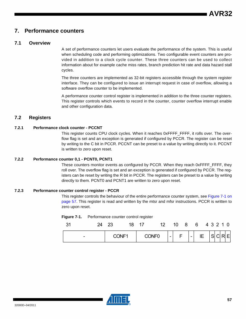
AVR32
7. Performance counters
7.1 OverviewA set of performance counters let users evaluate the performance of the system. This is usefulwhen scheduling code and performing optimizations. Two configurable event counters are pro-vided in addition to a clock cycle counter. These three counters can be used to collectinformation about for example cache miss rates, branch prediction hit rate and data hazard stallcycles.
The three counters are implemented as 32-bit registers accessible through the system registerinterface. They can be configured to issue an interrupt request in case of overflow, allowing asoftware overflow counter to be implemented.
A performance counter control register is implemented in addition to the three counter registers.This register controls which events to record in the counter, counter overflow interrupt enableand other configuration data.
7.2 Registers
7.2.1 Performance clock counter - PCCNTThis register counts CPU clock cycles. When it reaches 0xFFFF_FFFF, it rolls over. The over-flow flag is set and an exception is generated if configured by PCCR. The register can be resetby writing to the C bit in PCCR. PCCNT can be preset to a value by writing directly to it. PCCNTis written to zero upon reset.
7.2.2 Performance counter 0,1 - PCNT0, PCNT1These counters monitor events as configured by PCCR. When they reach 0xFFFF_FFFF, theyroll over. The overflow flag is set and an exception is generated if configured by PCCR. The reg-isters can be reset by writing the R bit in PCCR. The registers can be preset to a value by writingdirectly to them. PCNT0 and PCNT1 are written to zero upon reset.
7.2.3 Performance counter control register - PCCRThis register controls the behaviour of the entire performance counter system, see Figure 7-1 onpage 57. This register is read and written by the mtsr and mfsr instructions. PCCR is written tozero upon reset.
Figure 7-1. Performance counter control register
ERCSIE-F-CONF0CONF1-
012346810121718232431
5732000D–04/2011
The following fields exist in PCCR, see Table 7-1 on page 58.
Table 7-1. Performance counter control register
Bit Access Name Description
23:18 Read/write CONF1Configures which events to count with PCNT1. See Table 7-2 for a legend.
17:12 Read/write CONF0Configures which events to count with PCNT0. See Table 7-2 for a legend.
10:8 Read/write F
Interrupt flag. If read as 1, the corresponding overflow has occurred. Bit 8 corresponds to PCCNT.Bit 9 corresponds to PCNT0.
Bit 10 corresponds to PCNT1.
Flags are cleared by writing a 1 to the flag.
6:4 Read/write IE
Interrupt enable. If set, an overflow of the corresponding counter will cause an interrupt request.
Bit 4 corresponds to PCCNT.
Bit 5 corresponds to PCNT0.Bit 6 corresponds to PCNT1.
3 Read/write SClock counter scaler. If set, the clock counter increments once every 64’th clock cycle. This expands the period-to-overflow to 238 cycles.
2 Read-0/write C Clock counter reset. If written to 1, the clock counter will be reset.
1 Read-0/write RPerformance counter reset. If written to 1, all three counters will be reset.
0 Read/write EClock counter enable. If set, all three counters will count their configured events. If cleared, the counters are disabled and will not count.
OtherRead-0/write-0
- Unused. Read as 0. Should be written as 0.
5832000D–04/2011
AVR32
AVR32
7.3 Monitorable eventsThe following events can be monitored by the performance counters, depending on the settingof CONF0 and CONF1, see Table 7-2 on page 59.
Table 7-2. Monitorable events
Configure field setting Event monitored and counted
0x0Instruction cache miss. Incremented once for each instruction fetch from a cacheable memory area that did not hit in the cache.
0x1Instruction fetch stage stall. Incremented every cycle the memory system is unable to deliver an instruction to the CPU.
0x2 Data hazard stall. Incremented every cycle the condition is true.
0x3 ITLB miss.
0x4 DTLB miss.
0x5 Branch instruction executed. May or may not be taken.
0x6 Branch mispredicted.
0x7 Instruction executed. Incremented once each time an instruction is completed.
0x8 Stall due to data cache write buffers full. Incremented once for each occurrence.
0x9 Stall due to data cache write buffers full. Incremented every cycle the condition is true.
0xAStall due to data cache read miss. Incremented once for each data access to a cacheable memory area that did not hit in the cache.
0xBStall due to data cache read miss. Incremented every cycle the pipeline is stalled due to a data access to a cacheable memory area that did not hit in the cache.
0xC Write access counter. Incremented once for each write access.
0xD Write access counter. Incremented every cycle a write access is ongoing.
0xE Read access counter. Incremented once for each read access.
0xF Read access counter. Incremented every cycle a read access is ongoing.
0x10 Cache stall counter. Incremented once for each read or write access that stalls.
0x11Cache stall counter. Incremented every cycle a read or write access stalls. Write accesses are counted only until the write is put in the write buffer.
0x12 Cache access counter. Incremented once for each read or write access.
0x13Cache access counter. Incremented every cycle a read or write access is ongoing. Write accesses are counted only until the write is put in the write buffer.
0x14 Data cache line writeback. Incremented once when a line containing dirty data is replaced in the cache.
0x15 Accumulator cache hit
0x16 Accumulator cache miss
0x17 BTB hit. Incremented once per hit occurrence.
0x18 Micro-ITLB miss. Incremented once per miss occurrence.
0x19 Micro-DTLB miss. Incremented once per miss occurrence.
Other Reserved.
5932000D–04/2011
7.4 UsageThe performance counters can be used to monitor several different events and perform differentmeasurements. Some of the most useful are explained below.
7.4.1 Cycles per instructionCONF0: 0x7 (Instruction executed)
CPI = CCNT / PCNT0
Cycles-per-instruction (CPI) measures the average time it took to execute an instruction.
7.4.2 Icache miss rateCONF0: 0x7 (Instruction executed)
CONF1: 0x0 (Icache miss)
ICMR = PCNT1 / PCNT0
The instruction cache miss rate (ICMR) mesures the fraction of instruction cache misses perexecuted instruction.
7.4.3 Dcache read miss rateCONF0: 0xE (Dcache read access)
CONF1: 0xA (Dcache read miss)
DCMR = PCNT1 / PCNT0
The data cache read miss rate (DCRMR) mesures the fraction of data cache read misses perdata cache read access.
7.4.4 Average instruction fetch miss latencyCONF0: 0x1 (Instruction fetch stall)
CONF1: 0x0 (Icache miss)
AIFML = PCNT0 / PCNT1
The average instruction fetch miss latency (AIFML) mesures the average number of clock cyclesspent per instruction cache miss. This measure does not consider cycles spent due to ITLBmisses.
7.4.5 Fraction of execution time spent stalling due to instruction fetch missesCONF0: 0x1 (Instruction fetch stall)
AIFML = PCNT0 / PCCNT
The fraction of execution time spent stalling due to instruction fetch misses mesures the ratio ofclock cycles spent waiting for an instruction to be fetched to the total number of executioncycles.
7.4.6 Average writeback stall durationCONF0: 0x8 (Write buffer full occurrences)
CONF1: 0x9 (Write buffer full cycles)
6032000D–04/2011
AVR32
AVR32
AWSD = PCNT0 / PCNT1
The average writeback stall duration (AWSD) mesures the average number of clock cyclesspent stalling due to a full writebuffer.
7.4.7 Fraction of execution time spent stalling due to writebackCONF0: 0x9 (Write buffer full cycles)
FETW=CONF0/PCCNT
The fraction of execution time spent stalling due to writeback (FETW) is the ratio of writebufferfull stall cycles to the total number of cycles.
7.4.8 ITLB miss rateCONF0: 0x3 (ITLB miss)
CONF1: 0x7 (Instruction count)
IMR = PCNT0 / PCNT1
The ITLB miss rate (IMR) is the ratio of ITLB misses to the number of instructions executed.
7.4.9 DTLB miss rateCONF0: 0x4 (DTLB miss)
CONF1: 0x7 (Instruction count)
IMR = PCNT0 / PCNT1
The DTLB miss rate (DMR) is the ratio of DTLB misses to the number of instructions executed.
7.4.10 Branch prediction hit rateCONF0: 0x17 (BTB hit)
CONF1: 0x5 (Branch executed)
BPHR = PCNT0 / PCNT1
The branch prediction hit rate (BPHR) is the ratio of BTB hits to the number of branchesexecuted.
7.4.11 Branch prediction correct rateCONF0: 0x5 (Branch executed)
CONF1: 0x6 (Branch mispredicted)
BPCR = PCNT1 / PCNT0
The branch prediction correct rate (BPCR) is the ratio of branch mispredictions to the total num-ber of executed branches.
6132000D–04/2011

6232000D–04/2011
AVR32
AVR32
8. Event ProcessingDue to various reasons, the CPU may be required to abort normal program execution in order tohandle special, high-priority events. When handling of these events is complete, normal programexecution can be resumed. Traditionally, events that are generated internally in the CPU arecalled exceptions, while events generated by sources external to the CPU are called interrupts.The possible sources of events are listed in Table 8-1 on page 67.
The AVR32 has a powerful event handling scheme. The different event sources, like IllegalOpcode and external interrupt requests, have different priority levels, ensuring a well-definedbehaviour when multiple events are received simultaneously. Additionally, pending events of ahigher priority class may preempt handling of ongoing events of a lower priority class.
When an event occurs, the execution of the instruction stream is halted, and execution control ispassed to an event handler at an address specified in Table 8-1 on page 67. Most of the han-dlers are placed sequentially in the code space starting at the address specified by EVBA, withfour bytes between each handler. This gives ample space for a jump instruction to be placedthere, jumping to the event routine itself. A few critical handlers have larger spacing betweenthem, allowing the entire event routine to be placed directly at the address specified by theEVBA-relative offset generated by hardware. All external interrupt sources have autovectoredinterrupt service routine (ISR) addresses. This allows the interrupt controller to directly specifythe ISR address as an address relative to EVBA. The address range reachable by this autovec-tor offset is IMPLEMENTATION DEFINED. Implementations may require EVBA to be aligned inan IMPLEMENTATION DEFINED way in order to support autovectoring.
The same mechanisms are used to service all different types of events, including external inter-rupt requests, yielding a uniform event handling scheme.
If the application is executing in the secure state, the event handling is modified as explained in“Event handling in secure state” on page 92. This is to protect from hacking secure code usingthe event system.
8.1 Event handling in AVR32A
8.1.1 Exceptions and interrupt requestsWhen an event other than scall or debug request is received by the core, the following actionsare performed atomically:
1. The pending event will not be accepted if it is masked. The I3M, I2M, I1M, I0M, EM and GM bits in the Status Register are used to mask different events. Not all events can be masked. A few critical events (NMI, Unrecoverable Exception, TLB Multiple Hit and Bus Error) can not be masked. When an event is accepted, hardware automatically sets the mask bits corresponding to all sources with equal or lower priority. This inhibits accep-tance of other events of the same or lower priority, except for the critical events listed above. Software may choose to clear some or all of these bits after saving the neces-sary state if other priority schemes are desired. It is the event source’s responsability to ensure that their events are left pending until accepted by the CPU.
2. When a request is accepted, the Status Register and Program Counter of the current context is stored to the system stack. If the event is an INT0, INT1, INT2 or INT3, regis-ters R8 to R12 and LR are also automatically stored to stack. Storing the Status Register ensures that the core is returned to the previous execution mode when the current event handling is completed. When exceptions occur, both the EM and GM bits are set, and the application may manually enable nested exceptions if desired by clear-
6332000D–04/2011

ing the appropriate bit. Each exception handler has a dedicated handler address, and this address uniquely identifies the exception source.
3. The Mode bits are set to reflect the priority of the accepted event, and the correct regis-ter file bank is selected. The address of the event handler, as shown in Table 8-1, is loaded into the Program Counter.
The execution of the event handler routine then continues from the effective address calculated.
The rete instruction signals the end of the event. When encountered, the Return Status Registerand Return Address Register are popped from the system stack and restored to the Status Reg-ister and Program Counter. If the rete instruction returns from INT0, INT1, INT2 or INT3,registers R8 to R12 and LR are also popped from the system stack. The restored Status Regis-ter contains information allowing the core to resume operation in the previous execution mode.This concludes the event handling.
8.1.2 Supervisor callsThe AVR32 instruction set provides a supervisor mode call instruction. The scall instruction isdesigned so that privileged routines can be called from any context. This facilitates sharing ofcode between different execution modes. The scall mechanism is designed so that a minimalexecution cycle overhead is experienced when performing supervisor routine calls from time-critical event handlers.
The scall instruction behaves differently depending on which mode it is called from. The behav-iour is detailed in the instruction set reference. In order to allow the scall routine to return to thecorrect context, a return from supervisor call instruction, rets, is implemented. In the AVR32Amicroarchitecture, scall and rets uses the system stack to store the return address and the sta-tus register.
8.1.3 Debug requestsThe AVR32 architecture defines a dedicated debug mode. When a debug request is received bythe core, Debug mode is entered. Entry into Debug mode can be masked by the DM bit in thestatus register. Upon entry into Debug mode, hardware sets the SR[D] bit and jumps to theDebug Exception handler. By default, debug mode executes in the exception context, but withdedicated Return Address Register and Return Status Register. These dedicated registersremove the need for storing this data to the system stack, thereby improving debuggability. Themode bits in the status register can freely be manipulated in Debug mode, to observe registersin all contexts, while retaining full privileges.
Debug mode is exited by executing the retd instruction. This returns to the previous context.
8.2 Event handling in AVR32B
8.2.1 Exceptions and interrupt requestsWhen an event other than scall or debug request is received by the core, the following actionsare performed atomically:
1. The pending event will not be accepted if it is masked. The I3M, I2M, I1M, I0M, EM and GM bits in the Status Register are used to mask different events. Not all events can be masked. A few critical events (NMI, Unrecoverable Exception, TLB Multiple Hit and Bus Error) can not be masked. When an event is accepted, hardware automatically sets the mask bits corresponding to all sources with equal or lower priority. This inhibits accep-tance of other events of the same or lower priority, except for the critical events listed above. Software may choose to clear some or all of these bits after saving the neces-
6432000D–04/2011
AVR32
AVR32
sary state if other priority schemes are desired. It is the event source’s responsability to ensure that their events are left pending until accepted by the CPU.
2. When a request is accepted, the Status Register and Program Counter of the current context is stored in the Return Status Register and Return Address Register corre-sponding to the new context. Saving the Status Register ensures that the core is returned to the previous execution mode when the current event handling is completed. When exceptions occur, both the EM and GM bits are set, and the application may manually enable nested exceptions if desired by clearing the appropriate bit. Each exception handler has a dedicated handler address, and this address uniquely identi-fies the exception source.
3. The Mode bits are set correctly to reflect the priority of the accepted event, and the cor-rect register file banks are selected. The address of the event handler, as shown in Table 8-1, is loaded into the Program Counter.
The execution of the event routine then continues from the effective address calculated.
The rete instruction signals the end of the event. When encountered, the values in the ReturnStatus Register and Return Address Register corresponding to the event context are restored tothe Status Register and Program Counter. The restored Status Register contains informationallowing the core to resume operation in the previous execution mode. This concludes the eventhandling.
8.2.2 Supervisor callsThe AVR32 instruction set provides a supervisor mode call instruction. The scall instruction isdesigned so that privileged routines can be called from any context. This facilitates sharing ofcode between different execution modes. The scall mechanism is designed so that a minimalexecution cycle overhead is experienced when performing supervisor routine calls from time-critical event handlers.
The scall instruction behaves differently depending on which mode it is called from. The behav-iour is detailed in the instruction set reference. In order to allow the scall routine to return to thecorrect context, a return from supervisor call instruction, rets, is implemented.
8.2.3 Debug requestsThe AVR32 architecture defines a dedicated debug mode. When a debug request is received bythe core, Debug mode is entered. Entry into Debug mode can be masked by the DM bit in thestatus register. Upon entry into Debug mode, hardware sets the SR[D] bit and jumps to theDebug Exception handler. By default, debug mode executes in the exception context, but withdedicated Return Address Register and Return Status Register. These dedicated registersremove the need for storing this data to the system stack, thereby improving debuggability. Themode bits in the status register can freely be manipulated in Debug mode, to observe registersin all contexts, while retaining full privileges.
Debug mode is exited by executing the retd instruction. This returns to the previous context.
6532000D–04/2011
8.3 Entry points for eventsSeveral different event handler entry points exists. For AVR32A, the reset routine is placed ataddress 0x8000_0000. This places the reset address in the flash memory area. For AVR32B,the reset routine entry address is always fixed to 0xA000_0000. This address resides inunmapped, uncached space in order to ensure well-defined resets.
TLB miss exceptions and scall have a dedicated space relative to EVBA where their event han-dler can be placed. This speeds up execution by removing the need for a jump instruction placedat the program address jumped to by the event hardware. All other exceptions have a dedicatedevent routine entry point located relative to EVBA. The handler routine address identifies theexception source directly.
All external interrupt requests have entry points located at an offset relative to EVBA. Thisautovector offset is specified by an external Interrupt Controller. The programmer must makesure that none of the autovector offsets interfere with the placement of other code. The reach ofthe autovector offset is IMPLEMENTATION DEFINED.
Special considerations should be made when loading EVBA with a pointer. Due to security con-siderations, the event handlers should be located in the privileged address space, or in aprivileged memory protection region. In a system with MPU, the event routines could be placedin a cacheable protection region. In a segmented AVR32B system, some segments of the virtualmemory space may be better suited than others for holding event handlers. This is due to differ-ences in translateability and cacheability between segments. A cacheable, non-translatedsegment may offer the best performance for event handlers, as this will eliminate any TLBmisses and speed up instruction fetch. The user may also consider to lock the event handlers inthe instruction cache.
If several events occur on the same instruction, they are handled in a prioritized way. The priorityordering is presented in Table 8-1. If events occur on several instructions at different locations inthe pipeline, the events on the oldest instruction are always handled before any events on anyyounger instruction, even if the younger instruction has events of higher priority than the oldestinstruction. An instruction B is younger than an instruction A if it was sent down the pipeline laterthan A.
The addresses and priority of simultaneous events are shown in Table 8-1 on page 67
6632000D–04/2011
AVR32
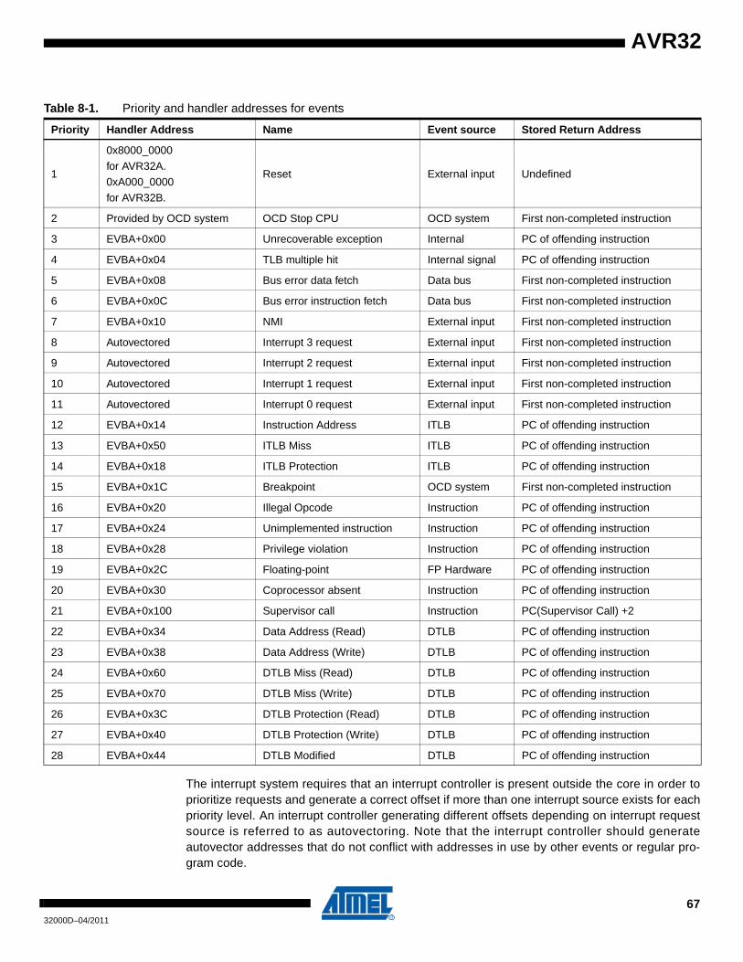
AVR32
The interrupt system requires that an interrupt controller is present outside the core in order toprioritize requests and generate a correct offset if more than one interrupt source exists for eachpriority level. An interrupt controller generating different offsets depending on interrupt requestsource is referred to as autovectoring. Note that the interrupt controller should generateautovector addresses that do not conflict with addresses in use by other events or regular pro-gram code.
Table 8-1. Priority and handler addresses for events
Priority Handler Address Name Event source Stored Return Address
1
0x8000_0000
for AVR32A.
0xA000_0000
for AVR32B.
Reset External input Undefined
2 Provided by OCD system OCD Stop CPU OCD system First non-completed instruction
3 EVBA+0x00 Unrecoverable exception Internal PC of offending instruction
4 EVBA+0x04 TLB multiple hit Internal signal PC of offending instruction
5 EVBA+0x08 Bus error data fetch Data bus First non-completed instruction
6 EVBA+0x0C Bus error instruction fetch Data bus First non-completed instruction
7 EVBA+0x10 NMI External input First non-completed instruction
8 Autovectored Interrupt 3 request External input First non-completed instruction
9 Autovectored Interrupt 2 request External input First non-completed instruction
10 Autovectored Interrupt 1 request External input First non-completed instruction
11 Autovectored Interrupt 0 request External input First non-completed instruction
12 EVBA+0x14 Instruction Address ITLB PC of offending instruction
13 EVBA+0x50 ITLB Miss ITLB PC of offending instruction
14 EVBA+0x18 ITLB Protection ITLB PC of offending instruction
15 EVBA+0x1C Breakpoint OCD system First non-completed instruction
16 EVBA+0x20 Illegal Opcode Instruction PC of offending instruction
17 EVBA+0x24 Unimplemented instruction Instruction PC of offending instruction
18 EVBA+0x28 Privilege violation Instruction PC of offending instruction
19 EVBA+0x2C Floating-point FP Hardware PC of offending instruction
20 EVBA+0x30 Coprocessor absent Instruction PC of offending instruction
21 EVBA+0x100 Supervisor call Instruction PC(Supervisor Call) +2
22 EVBA+0x34 Data Address (Read) DTLB PC of offending instruction
23 EVBA+0x38 Data Address (Write) DTLB PC of offending instruction
24 EVBA+0x60 DTLB Miss (Read) DTLB PC of offending instruction
25 EVBA+0x70 DTLB Miss (Write) DTLB PC of offending instruction
26 EVBA+0x3C DTLB Protection (Read) DTLB PC of offending instruction
27 EVBA+0x40 DTLB Protection (Write) DTLB PC of offending instruction
28 EVBA+0x44 DTLB Modified DTLB PC of offending instruction
6732000D–04/2011
The addresses of the interrupt routines are calculated by adding the address on the autovectoroffset bus to the value of the Exception Vector Base Address (EVBA). The INT0, INT1, INT2,INT3, and NMI signals indicate the priority of the pending interrupt. INT0 has the lowest priority,and NMI the highest priority of the interrupts. Implementations may require that EVBA is alignedin an IMPLEMENTATION DEFINED way in order to support autovectoring.
8.3.1 Description of events in AVR32A
8.3.1.1 Reset ExceptionThe Reset exception is generated when the reset input line to the CPU is asserted. The Resetexception can not be masked by any bit. The Reset exception resets all synchronous elementsand registers in the CPU pipeline to their default value, and starts execution of instructions ataddress 0x8000_0000.
SR = reset_value_of_SREG;
PC = 0x8000_0000;
All other system registers are reset to their reset value, which may or may not be defined. Referto the Programming Model chapter for details.
8.3.1.2 OCD Stop CPU ExceptionThe OCD Stop CPU exception is generated when the OCD Stop CPU input line to the CPU isasserted. The OCD Stop CPU exception can not be masked by any bit. This exception is identi-cal to a non-maskable, high priority breakpoint. Any subsequent operation is controlled by theOCD hardware. The OCD hardware will take control over the CPU and start to feed instructionsdirectly into the pipeline.
RSR_DBG = SR;
RAR_DBG = PC;
SR[M2:M0] = B’110;
SR[R] = 0;
SR[J] = 0;
SR[D] = 1;
SR[DM] = 1;
SR[EM] = 1;
SR[GM] = 1;
6832000D–04/2011
AVR32
AVR32
8.3.1.3 Unrecoverable ExceptionThe Unrecoverable Exception is generated when an exception request is issued when theException Mask (EM) bit in the status register is asserted. The Unrecoverable Exception can notbe masked by any bit. The Unrecoverable Exception is generated when a condition hasoccurred that the hardware cannot handle. The system will in most cases have to be restarted ifthis condition occurs.
*(--SPSYS) = PC of offending instruction;
*(--SPSYS) = SR;
SR[R] = 0;
SR[J] = 0;
SR[M2:M0] = B’110;
SR[EM] = 1;
SR[GM] = 1;
PC = EVBA + 0x00;
8.3.1.4 TLB Multiple Hit ExceptionTLB Multiple Hit exception is issued when multiple address matches occurs in the TLB, causingan internal inconsistency.
This exception signals a critical error where the hardware is in an undefined state. All interruptsare masked, and PC is loaded with EVBA + 0x04. MMU-related registers are updated with infor-mation in order to identify the failing address and the failing TLB if multiple TLBs are present.TLBEHI[ASID] is unchanged after the exception, and therefore identifies the ASID that causedthe exception.
TLBEAR = FAILING_VIRTUAL_ADDRESS;
TLBEHI[VPN] = FAILING_PAGE_NUMBER;
TLBEHI[I] = 0/1, depending on which TLB caused the error;
*(--SPSYS) = PC of offending instruction;
*(--SPSYS) = SR;
SR[R] = 0;
SR[J] = 0;
SR[M2:M0] = B’110;
SR[EM] = 1;
SR[GM] = 1;
PC = EVBA + 0x04;
6932000D–04/2011
8.3.1.5 Bus Error Exception on Data AccessThe Bus Error on Data Access exception is generated when the data bus detects an error condi-tion. This exception is caused by events unrelated to the instruction stream, or by data written tothe cache write-buffers many cycles ago. Therefore, execution can not be resumed in a safeway after this exception. The value placed in RAR_EX is unrelated to the operation that causedthe exception. The exception handler is responsible for performing the appropriate action.
*(--SPSYS) = PC of first non-issued instruction;
*(--SPSYS) = SR;
SR[R] = 0;
SR[J] = 0;
SR[M2:M0] = B’110;
SR[EM] = 1;
SR[GM] = 1;
PC = EVBA + 0x08;
8.3.1.6 Bus Error Exception on Instruction FetchThe Bus Error on Instruction Fetch exception is generated when the data bus detects an errorcondition. This exception is caused by events related to the instruction stream. Therefore, exe-cution can be restarted in a safe way after this exception, assuming that the condition thatcaused the bus error is dealt with.
*(--SPSYS) = PC of first non-issued instruction;
*(--SPSYS) = SR;
SR[R] = 0;
SR[J] = 0;
SR[M2:M0] = B’110;
SR[EM] = 1;
SR[GM] = 1;
PC = EVBA + 0x0C;
8.3.1.7 NMI ExceptionThe NMI exception is generated when the NMI input line to the core is asserted. The NMI excep-tion can not be masked by the SR[GM] bit. However, the core ignores the NMI input line whenprocessing an NMI Exception (the SR[M2:M0] bits are B’111). This guarantees serial executionof NMI Exceptions, and simplifies the NMI hardware and software mechanisms.
Since the NMI exception is unrelated to the instruction stream, the instructions in the pipeline areallowed to complete. After finishing the NMI exception routine, execution should continue at theinstruction following the last completed instruction in the instruction stream.
*(--SPSYS) = PC of first noncompleted instruction;
*(--SPSYS) = SR;
SR[R] = 0;
SR[J] = 0;
SR[M2:M0] = B’111;
SR[EM] = 1;
SR[GM] = 1;
PC = EVBA + 0x10;
7032000D–04/2011
AVR32
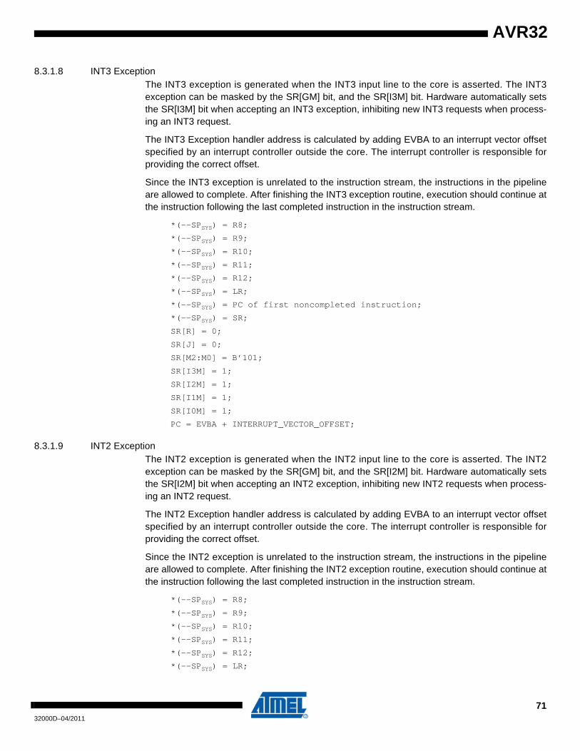
AVR32
8.3.1.8 INT3 ExceptionThe INT3 exception is generated when the INT3 input line to the core is asserted. The INT3exception can be masked by the SR[GM] bit, and the SR[I3M] bit. Hardware automatically setsthe SR[I3M] bit when accepting an INT3 exception, inhibiting new INT3 requests when process-ing an INT3 request.
The INT3 Exception handler address is calculated by adding EVBA to an interrupt vector offsetspecified by an interrupt controller outside the core. The interrupt controller is responsible forproviding the correct offset.
Since the INT3 exception is unrelated to the instruction stream, the instructions in the pipelineare allowed to complete. After finishing the INT3 exception routine, execution should continue atthe instruction following the last completed instruction in the instruction stream.
*(--SPSYS) = R8;
*(--SPSYS) = R9;
*(--SPSYS) = R10;
*(--SPSYS) = R11;
*(--SPSYS) = R12;
*(--SPSYS) = LR;
*(--SPSYS) = PC of first noncompleted instruction;
*(--SPSYS) = SR;
SR[R] = 0;
SR[J] = 0;
SR[M2:M0] = B’101;
SR[I3M] = 1;
SR[I2M] = 1;
SR[I1M] = 1;
SR[I0M] = 1;
PC = EVBA + INTERRUPT_VECTOR_OFFSET;
8.3.1.9 INT2 ExceptionThe INT2 exception is generated when the INT2 input line to the core is asserted. The INT2exception can be masked by the SR[GM] bit, and the SR[I2M] bit. Hardware automatically setsthe SR[I2M] bit when accepting an INT2 exception, inhibiting new INT2 requests when process-ing an INT2 request.
The INT2 Exception handler address is calculated by adding EVBA to an interrupt vector offsetspecified by an interrupt controller outside the core. The interrupt controller is responsible forproviding the correct offset.
Since the INT2 exception is unrelated to the instruction stream, the instructions in the pipelineare allowed to complete. After finishing the INT2 exception routine, execution should continue atthe instruction following the last completed instruction in the instruction stream.
*(--SPSYS) = R8;
*(--SPSYS) = R9;
*(--SPSYS) = R10;
*(--SPSYS) = R11;
*(--SPSYS) = R12;
*(--SPSYS) = LR;
7132000D–04/2011
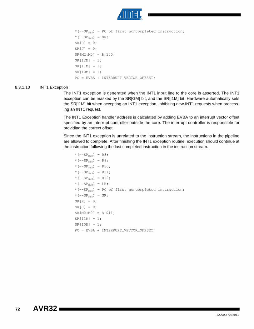
*(--SPSYS) = PC of first noncompleted instruction;
*(--SPSYS) = SR;
SR[R] = 0;
SR[J] = 0;
SR[M2:M0] = B’100;
SR[I2M] = 1;
SR[I1M] = 1;
SR[I0M] = 1;
PC = EVBA + INTERRUPT_VECTOR_OFFSET;
8.3.1.10 INT1 ExceptionThe INT1 exception is generated when the INT1 input line to the core is asserted. The INT1exception can be masked by the SR[GM] bit, and the SR[I1M] bit. Hardware automatically setsthe SR[I1M] bit when accepting an INT1 exception, inhibiting new INT1 requests when process-ing an INT1 request.
The INT1 Exception handler address is calculated by adding EVBA to an interrupt vector offsetspecified by an interrupt controller outside the core. The interrupt controller is responsible forproviding the correct offset.
Since the INT1 exception is unrelated to the instruction stream, the instructions in the pipelineare allowed to complete. After finishing the INT1 exception routine, execution should continue atthe instruction following the last completed instruction in the instruction stream.
*(--SPSYS) = R8;
*(--SPSYS) = R9;
*(--SPSYS) = R10;
*(--SPSYS) = R11;
*(--SPSYS) = R12;
*(--SPSYS) = LR;
*(--SPSYS) = PC of first noncompleted instruction;
*(--SPSYS) = SR;
SR[R] = 0;
SR[J] = 0;
SR[M2:M0] = B’011;
SR[I1M] = 1;
SR[I0M] = 1;
PC = EVBA + INTERRUPT_VECTOR_OFFSET;
7232000D–04/2011
AVR32

AVR32
8.3.1.11 INT0 ExceptionThe INT0 exception is generated when the INT0 input line to the core is asserted. The INT0exception can be masked by the SR[GM] bit, and the SR[I0M] bit. Hardware automatically setsthe SR[I0M] bit when accepting an INT0 exception, inhibiting new INT0 requests when process-ing an INT0 request.
The INT0 Exception handler address is calculated by adding EVBA to an interrupt vector offsetspecified by an interrupt controller outside the core. The interrupt controller is responsible forproviding the correct offset.
Since the INT0 exception is unrelated to the instruction stream, the instructions in the pipelineare allowed to complete. After finishing the INT0 exception routine, execution should continue atthe instruction following the last completed instruction in the instruction stream.
*(--SPSYS) = R8;
*(--SPSYS) = R9;
*(--SPSYS) = R10;
*(--SPSYS) = R11;
*(--SPSYS) = R12;
*(--SPSYS) = LR;
*(--SPSYS) = PC of first noncompleted instruction;
*(--SPSYS) = SR;
SR[R] = 0;
SR[J] = 0;
SR[M2:M0] = B’010;
SR[I0M] = 1;
PC = EVBA + INTERRUPT_VECTOR_OFFSET;
8.3.1.12 Instruction Address ExceptionThe Instruction Address Error exception is generated if the generated instruction memoryaddress has an illegal alignment.
*(--SPSYS) = PC;
*(--SPSYS) = SR;
TLBEAR = FAILING_VIRTUAL_ADDRESS;
TLBEHI[VPN] = FAILING_PAGE_NUMBER;
SR[R] = 0;
SR[J] = 0;
SR[M2:M0] = B’110;
SR[EM] = 1;
SR[GM] = 1;
PC = EVBA + 0x14;
7332000D–04/2011

8.3.1.13 ITLB Miss ExceptionThe ITLB Miss exception is generated when no TLB entry matches the instruction memoryaddress, or if the Valid bit in a matching entry is 0.
*(--SPSYS) = PC;
*(--SPSYS) = SR;
TLBEAR = FAILING_VIRTUAL_ADDRESS;
TLBEHI[VPN] = FAILING_PAGE_NUMBER;
TLBEHI[I] = 1;
SR[R] = 0;
SR[J] = 0;
SR[M2:M0] = B’110;
SR[EM] = 1;
SR[GM] = 1;
PC = EVBA + 0x50;
8.3.1.14 ITLB Protection ExceptionThe ITLB Protection exception is generated when the instruction memory access violates theaccess rights specified by the protection bits of the addressed virtual page.
*(--SPSYS) = PC;
*(--SPSYS) = SR;
TLBEAR = FAILING_VIRTUAL_ADDRESS;
TLBEHI[VPN] = FAILING_PAGE_NUMBER;
TLBEHI[I] = 1;
SR[R] = 0;
SR[J] = 0;
SR[M2:M0] = B’110;
SR[EM] = 1;
SR[GM] = 1;
PC = EVBA + 0x18;
7432000D–04/2011
AVR32
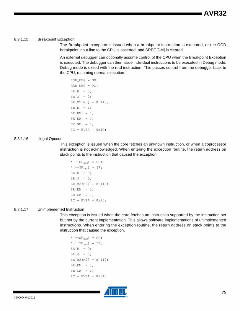
AVR32
8.3.1.15 Breakpoint ExceptionThe Breakpoint exception is issued when a breakpoint instruction is executed, or the OCDbreakpoint input line to the CPU is asserted, and SREG[DM] is cleared.
An external debugger can optionally assume control of the CPU when the Breakpoint Exceptionis executed. The debugger can then issue individual instructions to be executed in Debug mode.Debug mode is exited with the retd instruction. This passes control from the debugger back tothe CPU, resuming normal execution.
RSR_DBG = SR;
RAR_DBG = PC;
SR[R] = 0;
SR[J] = 0;
SR[M2:M0] = B’110;
SR[D] = 1;
SR[DM] = 1;
SR[EM] = 1;
SR[GM] = 1;
PC = EVBA + 0x1C;
8.3.1.16 Illegal OpcodeThis exception is issued when the core fetches an unknown instruction, or when a coprocessorinstruction is not acknowledged. When entering the exception routine, the return address onstack points to the instruction that caused the exception.
*(--SPSYS) = PC;
*(--SPSYS) = SR;
SR[R] = 0;
SR[J] = 0;
SR[M2:M0] = B’110;
SR[EM] = 1;
SR[GM] = 1;
PC = EVBA + 0x20;
8.3.1.17 Unimplemented InstructionThis exception is issued when the core fetches an instruction supported by the instruction setbut not by the current implementation. This allows software implementations of unimplementedinstructions. When entering the exception routine, the return address on stack points to theinstruction that caused the exception.
*(--SPSYS) = PC;
*(--SPSYS) = SR;
SR[R] = 0;
SR[J] = 0;
SR[M2:M0] = B’110;
SR[EM] = 1;
SR[GM] = 1;
PC = EVBA + 0x24;
7532000D–04/2011
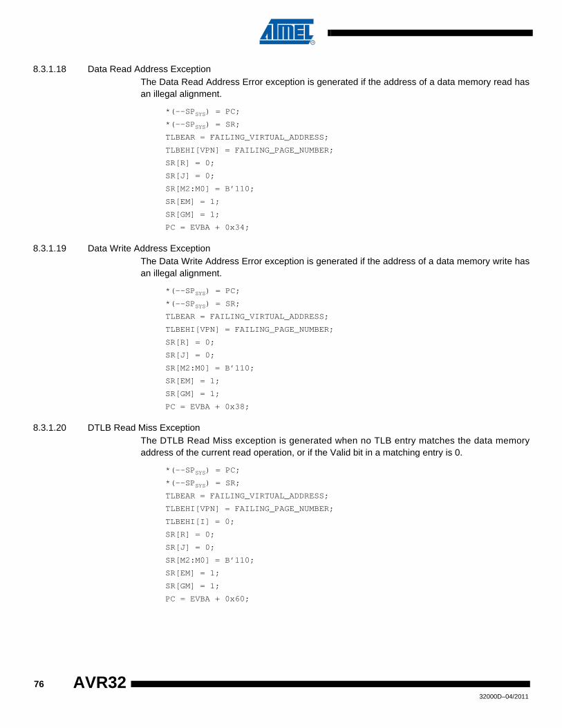
8.3.1.18 Data Read Address ExceptionThe Data Read Address Error exception is generated if the address of a data memory read hasan illegal alignment.
*(--SPSYS) = PC;
*(--SPSYS) = SR;
TLBEAR = FAILING_VIRTUAL_ADDRESS;
TLBEHI[VPN] = FAILING_PAGE_NUMBER;
SR[R] = 0;
SR[J] = 0;
SR[M2:M0] = B’110;
SR[EM] = 1;
SR[GM] = 1;
PC = EVBA + 0x34;
8.3.1.19 Data Write Address ExceptionThe Data Write Address Error exception is generated if the address of a data memory write hasan illegal alignment.
*(--SPSYS) = PC;
*(--SPSYS) = SR;
TLBEAR = FAILING_VIRTUAL_ADDRESS;
TLBEHI[VPN] = FAILING_PAGE_NUMBER;
SR[R] = 0;
SR[J] = 0;
SR[M2:M0] = B’110;
SR[EM] = 1;
SR[GM] = 1;
PC = EVBA + 0x38;
8.3.1.20 DTLB Read Miss ExceptionThe DTLB Read Miss exception is generated when no TLB entry matches the data memoryaddress of the current read operation, or if the Valid bit in a matching entry is 0.
*(--SPSYS) = PC;
*(--SPSYS) = SR;
TLBEAR = FAILING_VIRTUAL_ADDRESS;
TLBEHI[VPN] = FAILING_PAGE_NUMBER;
TLBEHI[I] = 0;
SR[R] = 0;
SR[J] = 0;
SR[M2:M0] = B’110;
SR[EM] = 1;
SR[GM] = 1;
PC = EVBA + 0x60;
7632000D–04/2011
AVR32
AVR32
8.3.1.21 DTLB Write Miss ExceptionThe DTLB Write Miss exception is generated when no TLB entry matches the data memoryaddress of the current write operation, or if the Valid bit in a matching entry is 0.
*(--SPSYS) = PC;
*(--SPSYS) = SR;
TLBEAR = FAILING_VIRTUAL_ADDRESS;
TLBEHI[VPN] = FAILING_PAGE_NUMBER;
TLBEHI[I] = 0;
SR[R] = 0;
SR[J] = 0;
SR[M2:M0] = B’110;
SR[EM] = 1;
SR[GM] = 1;
PC = EVBA + 0x70;
8.3.1.22 DTLB Read Protection ExceptionThe DTLB Protection exception is generated when the data memory read violates the accessrights specified by the protection bits of the addressed virtual page.
*(--SPSYS) = PC;
*(--SPSYS) = SR;
TLBEAR = FAILING_VIRTUAL_ADDRESS;
TLBEHI[VPN] = FAILING_PAGE_NUMBER;
TLBEHI[I] = 0;
SR[R] = 0;
SR[J] = 0;
SR[M2:M0] = B’110;
SR[EM] = 1;
SR[GM] = 1;
PC = EVBA + 0x3C;
8.3.1.23 DTLB Write Protection ExceptionThe DTLB Protection exception is generated when the data memory write violates the accessrights specified by the protection bits of the addressed virtual page.
*(--SPSYS) = PC;
*(--SPSYS) = SR;
TLBEAR = FAILING_VIRTUAL_ADDRESS;
TLBEHI[VPN] = FAILING_PAGE_NUMBER;
TLBEHI[I] = 0;
SR[R] = 0;
SR[J] = 0;
SR[M2:M0] = B’110;
SR[EM] = 1;
SR[GM] = 1;
PC = EVBA + 0x40;
7732000D–04/2011
8.3.1.24 Privilege Violation ExceptionIf the application tries to execute privileged instructions, this exception is issued. The completelist of priveleged instructions is shown in Table 8-2 on page 78. When entering the exceptionroutine, the address of the instruction that caused the exception is stored as the stacked returnaddress.
*(--SPSYS) = PC;
*(--SPSYS) = SR;
SR[R] = 0;
SR[J] = 0;
SR[M2:M0] = B’110;
SR[EM] = 1;
SR[GM] = 1;
PC = EVBA + 0x28;
Table 8-2. List of instructions which can only execute in privileged modes.
Privileged Instructions Comment
csrf - clear status register flag Privileged only when accessing upper half of status register
cache - perform cache operation
tlbr - read addressed TLB entry into TLBEHI and TLBELO
tlbw - write TLB entry registers into TLB
tlbs - search TLB for entry matching TLBEHI[VPN]
mtsr - move to system register Unpriviledged when accessing JOSP and JECR
mfsr - move from system register Unpriviledged when accessing JOSP and JECR
mtdr - move to debug register
mfdr - move from debug register
rete- return from exception
rets - return from supervisor call
retd - return from debug mode
sleep - sleep
ssrf - set status register flag Privileged only when accessing upper half of status register
7832000D–04/2011
AVR32
AVR32
8.3.1.25 DTLB Modified ExceptionThe DTLB Modified exception is generated when a data memory write hits a valid TLB entry, butthe Dirty bit of the entry is 0. This indicates that the page is not writable.
*(--SPSYS) = PC;
*(--SPSYS) = SR;
TLBEAR = FAILING_VIRTUAL_ADDRESS;
TLBEHI[VPN] = FAILING_PAGE_NUMBER;
TLBEHI[I] = 0;
SR[R] = 0;
SR[J] = 0;
SR[M2:M0] = B’110;
SR[EM] = 1;
SR[GM] = 1;
PC = EVBA + 0x44;
8.3.1.26 Floating-point ExceptionThe Floating-point exception is generated when the optional Floating-Point Hardware signalsthat an IEEE exception occurred, or when another type of error from the floating-point hardwareoccurred..
*(--SPSYS) = PC;
*(--SPSYS) = SR;
SR[R] = 0;
SR[J] = 0;
SR[M2:M0] = B’110;
SR[EM] = 1;
SR[GM] = 1;
PC = EVBA + 0x2C;
8.3.1.27 Coprocessor ExceptionThe Coprocessor exception occurs when the addressed coprocessor does not acknowledge aninstruction. This permits software implementation of coprocessors.
*(--SPSYS) = PC;
*(--SPSYS) = SR;
SR[R] = 0;
SR[J] = 0;
SR[M2:M0] = B’110;
SR[EM] = 1;
SR[GM] = 1;
PC = EVBA + 0x30;
7932000D–04/2011
8.3.1.28 Supervisor callSupervisor calls are signalled by the application code executing a supervisor call (scall) instruc-tion. The scall instruction behaves differently depending on which context it is called from. Thisallows scall to be called from other contexts than Application.
When the exception routine is finished, execution continues at the instruction following scall. Therets instruction is used to return from supervisor calls.
If ( SR[M2:M0] == {B’000 or B’001} )
*(--SPSYS) = PC;
*(--SPSYS) = SR;
PC ← EVBA + 0x100;
SR[M2:M0] ← B’001;
else
LRCurrent Context ← PC + 2;
PC ← EVBA + 0x100;
8032000D–04/2011
AVR32

AVR32
8.3.2 Description of events in AVR32B
8.3.2.1 Reset ExceptionThe Reset exception is generated when the reset input line to the CPU is asserted. The Resetexception can not be masked by any bit. The Reset exception resets all synchronous elementsand registers in the CPU pipeline to their default value, and starts execution of instructions ataddress 0xA000_0000.
SR = reset_value_of_SREG;
PC = 0xA000_0000;
All other system registers are reset to their reset value, which may or may not be defined. Referto the Programming Model chapter for details.
8.3.2.2 OCD Stop CPU ExceptionThe OCD Stop CPU exception is generated when the OCD Stop CPU input line to the CPU isasserted. The OCD Stop CPU exception can not be masked by any bit. This exception is identi-cal to a non-maskable, high priority breakpoint. Any subsequent operation is controlled by theOCD hardware. The OCD hardware will take control over the CPU and start to feed instructionsdirectly into the pipeline.
RSR_DBG = SR;
RAR_DBG = PC;
SR[M2:M0] = B’110;
SR[R] = 0;
SR[J] = 0;
SR[D] = 1;
SR[DM] = 1;
SR[EM] = 1;
SR[GM] = 1;
8.3.2.3 Unrecoverable ExceptionThe Unrecoverable Exception is generated when an exception request is issued when theException Mask (EM) bit in the status register is asserted. The Unrecoverable Exception can notbe masked by any bit. The Unrecoverable Exception is generated when a condition hasoccurred that the hardware cannot handle. The system will in most cases have to be restarted ifthis condition occurs.
RSR_EX = SR;
RAR_EX = PC of offending instruction;
SR[R] = 0;
SR[J] = 0;
SR[M2:M0] = B’110;
SR[EM] = 1;
SR[GM] = 1;
PC = EVBA + 0x00;
8132000D–04/2011
8.3.2.4 TLB Multiple Hit ExceptionTLB Multiple Hit exception is issued when multiple address matches occurs in the TLB, causingan internal inconsistency.
This exception signals a critical error where the hardware is in an undefined state. All interruptsare masked, and PC is loaded with EVBA + 0x04. MMU-related registers are updated with infor-mation in order to identify the failing address and the failing TLB if multiple TLBs are present.TLBEHI[ASID] is unchanged after the exception, and therefore identifies the ASID that causedthe exception.
RSR_EX = SR;
RAR_EX = PC of offending instruction;
TLBEAR = FAILING_VIRTUAL_ADDRESS;
TLBEHI[VPN] = FAILING_PAGE_NUMBER;
TLBEHI[I] = 0/1, depending on which TLB caused the error;
SR[R] = 0;
SR[J] = 0;
SR[M2:M0] = B’110;
SR[EM] = 1;
SR[GM] = 1;
PC = EVBA + 0x04;
8.3.2.5 Bus Error Exception on Data AccessThe Bus Error on Data Access exception is generated when the data bus detects an error condi-tion. This exception is caused by events unrelated to the instruction stream, or by data written tothe cache write-buffers many cycles ago. Therefore, execution can not be resumed in a safeway after this exception. The value placed in RAR_EX is unrelated to the operation that causedthe exception. The exception handler is responsible for performing the appropriate action.
RSR_EX = SR;
RAR_EX = PC of first non-issued instruction;
SR[R] = 0;
SR[J] = 0;
SR[M2:M0] = B’110;
SR[EM] = 1;
SR[GM] = 1;
PC = EVBA + 0x08;
8.3.2.6 Bus Error Exception on Instruction FetchThe Bus Error on Instruction Fetch exception is generated when the data bus detects an errorcondition. This exception is caused by events related to the instruction stream. Therefore, exe-cution can be restarted in a safe way after this exception, assuming that the condition thatcaused the bus error is dealt with.
RSR_EX = SR;
RAR_EX = PC;
SR[R] = 0;
SR[J] = 0;
SR[M2:M0] = B’110;
SR[EM] = 1;
8232000D–04/2011
AVR32

AVR32
SR[GM] = 1;
PC = EVBA + 0x0C;
8.3.2.7 NMI ExceptionThe NMI exception is generated when the NMI input line to the core is asserted. The NMI excep-tion can not be masked by the SR[GM] bit. However, the core ignores the NMI input line whenprocessing an NMI Exception (the SR[M2:M0] bits are B’111). This guarantees serial executionof NMI Exceptions, and simplifies the NMI hardware and software mechanisms.
Since the NMI exception is unrelated to the instruction stream, the instructions in the pipeline areallowed to complete. After finishing the NMI exception routine, execution should continue at theinstruction following the last completed instruction in the instruction stream.
RSR_NMI = SR;
RAR_NMI = Address of first noncompleted instruction;
SR[R] = 0;
SR[J] = 0;
SR[M2:M0] = B’111;
SR[EM] = 1;
SR[GM] = 1;
PC = EVBA + 0x10;
8.3.2.8 INT3 ExceptionThe INT3 exception is generated when the INT3 input line to the core is asserted. The INT3exception can be masked by the SR[GM] bit, and the SR[I3M] bit. Hardware automatically setsthe SR[I3M] bit when accepting an INT3 exception, inhibiting new INT3 requests when process-ing an INT3 request.
The INT3 Exception handler address is calculated by adding EVBA to an interrupt vector offsetspecified by an interrupt controller outside the core. The interrupt controller is responsible forproviding the correct offset.
Since the INT3 exception is unrelated to the instruction stream, the instructions in the pipelineare allowed to complete. After finishing the INT3 exception routine, execution should continue atthe instruction following the last completed instruction in the instruction stream.
RSR_INT3 = SR;
RAR_INT3 = Address of first noncompleted instruction;
SR[R] = 0;
SR[J] = 0;
SR[M2:M0] = B’101;
SR[I3M] = 1;
SR[I2M] = 1;
SR[I1M] = 1;
SR[I0M] = 1;
PC = EVBA + INTERRUPT_VECTOR_OFFSET;
8332000D–04/2011

8.3.2.9 INT2 ExceptionThe INT2 exception is generated when the INT2 input line to the core is asserted. The INT2exception can be masked by the SR[GM] bit, and the SR[I2M] bit. Hardware automatically setsthe SR[I2M] bit when accepting an INT2 exception, inhibiting new INT2 requests when process-ing an INT2 request.
The INT2 Exception handler address is calculated by adding EVBA to an interrupt vector offsetspecified by an interrupt controller outside the core. The interrupt controller is responsible forproviding the correct offset.
Since the INT2 exception is unrelated to the instruction stream, the instructions in the pipelineare allowed to complete. After finishing the INT2 exception routine, execution should continue atthe instruction following the last completed instruction in the instruction stream.
RSR_INT2 = SR;
RAR_INT2 = Address of first noncompleted instruction;
SR[R] = 0;
SR[J] = 0;
SR[M2:M0] = B’100;
SR[I2M] = 1;
SR[I1M] = 1;
SR[I0M] = 1;
PC = EVBA + INTERRUPT_VECTOR_OFFSET;
8.3.2.10 INT1 ExceptionThe INT1 exception is generated when the INT1 input line to the core is asserted. The INT1exception can be masked by the SR[GM] bit, and the SR[I1M] bit. Hardware automatically setsthe SR[I1M] bit when accepting an INT1 exception, inhibiting new INT1 requests when process-ing an INT1 request.
The INT1 Exception handler address is calculated by adding EVBA to an interrupt vector offsetspecified by an interrupt controller outside the core. The interrupt controller is responsible forproviding the correct offset.
Since the INT1 exception is unrelated to the instruction stream, the instructions in the pipelineare allowed to complete. After finishing the INT1 exception routine, execution should continue atthe instruction following the last completed instruction in the instruction stream.
RSR_INT1 = SR;
RAR_INT1 = Address of first noncompleted instruction;
SR[R] = 0;
SR[J] = 0;
SR[M2:M0] = B’011;
SR[I1M] = 1;
SR[I0M] = 1;
PC = EVBA + INTERRUPT_VECTOR_OFFSET;
8432000D–04/2011
AVR32
AVR32
8.3.2.11 INT0 ExceptionThe INT0 exception is generated when the INT0 input line to the core is asserted. The INT0exception can be masked by the SR[GM] bit, and the SR[I0M] bit. Hardware automatically setsthe SR[I0M] bit when accepting an INT0 exception, inhibiting new INT0 requests when process-ing an INT0 request.
The INT0 Exception handler address is calculated by adding EVBA to an interrupt vector offsetspecified by an interrupt controller outside the core. The interrupt controller is responsible forproviding the correct offset.
Since the INT0 exception is unrelated to the instruction stream, the instructions in the pipelineare allowed to complete. After finishing the INT0 exception routine, execution should continue atthe instruction following the last completed instruction in the instruction stream.
RSR_INT0 = SR;
RAR_INT0 = Address of first noncompleted instruction;
SR[R] = 0;
SR[J] = 0;
SR[M2:M0] = B’010;
SR[I0M] = 1;
PC = EVBA + INTERRUPT_VECTOR_OFFSET;
8.3.2.12 Instruction Address ExceptionThe Instruction Address Error exception is generated if the generated instruction memoryaddress has an illegal alignment.
RSR_EX = SR;
RAR_EX = PC;
TLBEAR = FAILING_VIRTUAL_ADDRESS;
TLBEHI[VPN] = FAILING_PAGE_NUMBER;
SR[R] = 0;
SR[J] = 0;
SR[M2:M0] = B’110;
SR[EM] = 1;
SR[GM] = 1;
PC = EVBA + 0x14;
8532000D–04/2011
8.3.2.13 ITLB Miss ExceptionThe ITLB Miss exception is generated when no TLB entry matches the instruction memoryaddress, or if the Valid bit in a matching entry is 0.
RSR_EX = SR;
RAR_EX = PC;
TLBEAR = FAILING_VIRTUAL_ADDRESS;
TLBEHI[VPN] = FAILING_PAGE_NUMBER;
TLBEHI[I] = 1;
SR[R] = 0;
SR[J] = 0;
SR[M2:M0] = B’110;
SR[EM] = 1;
SR[GM] = 1;
PC = EVBA + 0x50;
8.3.2.14 ITLB Protection ExceptionThe ITLB Protection exception is generated when the instruction memory access violates theaccess rights specified by the protection bits of the addressed virtual page.
RSR_EX = SR;
RAR_EX = PC;
TLBEAR = FAILING_VIRTUAL_ADDRESS;
TLBEHI[VPN] = FAILING_PAGE_NUMBER;
TLBEHI[I] = 1;
SR[R] = 0;
SR[J] = 0;
SR[M2:M0] = B’110;
SR[EM] = 1;
SR[GM] = 1;
PC = EVBA + 0x18;
8.3.2.15 Breakpoint ExceptionThe Breakpoint exception is issued when a breakpoint instruction is executed, or the OCDbreakpoint input line to the CPU is asserted, and SREG[DM] is cleared.
An external debugger can optionally assume control of the CPU when the Breakpoint Exceptionis executed. The debugger can then issue individual instructions to be executed in Debug mode.Debug mode is exited with the retd instruction. This passes control from the debugger back tothe CPU, resuming normal execution.
RSR_DBG = SR;
RAR_DBG = PC;
SR[R] = 0;
SR[J] = 0;
SR[M2:M0] = B’110;
SR[D] = 1;
SR[DM] = 1;
8632000D–04/2011
AVR32
AVR32
SR[EM] = 1;
SR[GM] = 1;
PC = EVBA + 0x1C;
8.3.2.16 Illegal OpcodeThis exception is issued when the core fetches an unknown instruction, or when a coprocessorinstruction is not acknowledged. When entering the exception routine, the return address onstack points to the instruction that caused the exception.
RSR_EX = SR;
RAR_EX = PC;
SR[R] = 0;
SR[J] = 0;
SR[M2:M0] = B’110;
SR[EM] = 1;
SR[GM] = 1;
PC = EVBA + 0x20;
8.3.2.17 Unimplemented InstructionThis exception is issued when the core fetches an instruction supported by the instruction setbut not by the current implementation. This allows software implementations of unimplementedinstructions. When entering the exception routine, the return address on stack points to theinstruction that caused the exception.
RSR_EX = SR;
RAR_EX = PC;
SR[R] = 0;
SR[J] = 0;
SR[M2:M0] = B’110;
SR[EM] = 1;
SR[GM] = 1;
PC = EVBA + 0x24;
8.3.2.18 Data Read Address ExceptionThe Data Read Address Error exception is generated if the address of a data memory read hasan illegal alignment.
RSR_EX = SR;
RAR_EX = PC;
TLBEAR = FAILING_VIRTUAL_ADDRESS;
TLBEHI[VPN] = FAILING_PAGE_NUMBER;
SR[R] = 0;
SR[J] = 0;
SR[M2:M0] = B’110;
SR[EM] = 1;
SR[GM] = 1;
PC = EVBA + 0x34;
8732000D–04/2011
8.3.2.19 Data Write Address ExceptionThe Data Write Address Error exception is generated if the address of a data memory write hasan illegal alignment.
RSR_EX = SR;
RAR_EX = PC;
TLBEAR = FAILING_VIRTUAL_ADDRESS;
TLBEHI[VPN] = FAILING_PAGE_NUMBER;
SR[R] = 0;
SR[J] = 0;
SR[M2:M0] = B’110;
SR[EM] = 1;
SR[GM] = 1;
PC = EVBA + 0x38;
8.3.2.20 DTLB Read Miss ExceptionThe DTLB Read Miss exception is generated when no TLB entry matches the data memoryaddress of the current read operation, or if the Valid bit in a matching entry is 0.
RSR_EX = SR;
RAR_EX = PC;
TLBEAR = FAILING_VIRTUAL_ADDRESS;
TLBEHI[VPN] = FAILING_PAGE_NUMBER;
TLBEHI[I] = 0;
SR[R] = 0;
SR[J] = 0;
SR[M2:M0] = B’110;
SR[EM] = 1;
SR[GM] = 1;
PC = EVBA + 0x60;
8.3.2.21 DTLB Write Miss ExceptionThe DTLB Write Miss exception is generated when no TLB entry matches the data memoryaddress of the current write operation, or if the Valid bit in a matching entry is 0.
RSR_EX = SR;
RAR_EX = PC;
TLBEAR = FAILING_VIRTUAL_ADDRESS;
TLBEHI[VPN] = FAILING_PAGE_NUMBER;
TLBEHI[I] = 0;
SR[R] = 0;
SR[J] = 0;
SR[M2:M0] = B’110;
SR[EM] = 1;
SR[GM] = 1;
PC = EVBA + 0x70;
8832000D–04/2011
AVR32
AVR32
8.3.2.22 DTLB Read Protection ExceptionThe DTLB Protection exception is generated when the data memory read violates the accessrights specified by the protection bits of the addressed virtual page.
RSR_EX = SR;
RAR_EX = PC;
TLBEAR = FAILING_VIRTUAL_ADDRESS;
TLBEHI[VPN] = FAILING_PAGE_NUMBER;
TLBEHI[I] = 0;
SR[R] = 0;
SR[J] = 0;
SR[M2:M0] = B’110;
SR[EM] = 1;
SR[GM] = 1;
PC = EVBA + 0x3C;
8.3.2.23 DTLB Write Protection ExceptionThe DTLB Protection exception is generated when the data memory write violates the accessrights specified by the protection bits of the addressed virtual page.
RSR_EX = SR;
RAR_EX = PC;
TLBEAR = FAILING_VIRTUAL_ADDRESS;
TLBEHI[VPN] = FAILING_PAGE_NUMBER;
TLBEHI[I] = 0;
SR[R] = 0;
SR[J] = 0;
SR[M2:M0] = B’110;
SR[EM] = 1;
SR[GM] = 1;
PC = EVBA + 0x40;
8.3.2.24 Privilege Violation ExceptionIf the application tries to execute privileged instructions, this exception is issued. The completelist of priveleged instructions is shown in Table 8-2. When entering the exception routine, theaddress of the instruction that caused the exception is stored as yhe stacked return address.
RSR_EX = SR;
RAR_EX = PC;
SR[R] = 0;
SR[J] = 0;
SR[M2:M0] = B’110;
SR[EM] = 1;
SR[GM] = 1;
PC = EVBA + 0x28;
8932000D–04/2011

8.3.2.25 DTLB Modified ExceptionThe DTLB Modified exception is generated when a data memory write hits a valid TLB entry, butthe Dirty bit of the entry is 0. This indicates that the page is not writable.
RSR_EX = SR;
RAR_EX = PC;
TLBEAR = FAILING_VIRTUAL_ADDRESS;
TLBEHI[VPN] = FAILING_PAGE_NUMBER;
TLBEHI[I] = 0;
SR[R] = 0;
SR[J] = 0;
SR[M2:M0] = B’110;
SR[EM] = 1;
SR[GM] = 1;
PC = EVBA + 0x44;
Table 8-3. List of instructions which can only execute in privileged modes.
Privileged Instructions Comment
csrf - clear status register flag Privileged only when accessing upper half of status register
cache - perform cache operation
tlbr - read addressed TLB entry into TLBEHI and TLBELO
tlbw - write TLB entry registers into TLB
tlbs - search TLB for entry matching TLBEHI[VPN]
mtsr - move to system register Unpriviledged when accessing JOSP and JECR
mfsr - move from system register Unpriviledged when accessing JOSP and JECR
- move to debug register
mfdr - move from debug register
rete- return from exception
rets - return from supervisor call
retd - return from debug mode
sleep - sleep
ssrf - set status register flag Privileged only when accessing upper half of status register
9032000D–04/2011
AVR32
AVR32
8.3.2.26 Floating-point ExceptionThe Floating-point exception is generated when the optional Floating-Point Hardware signalsthat an IEEE exception occurred, or when another type of error from the floating-point hardwareoccurred..
RSR_EX = SR;
RAR_EX = PC;
SR[R] = 0;
SR[J] = 0;
SR[M2:M0] = B’110;
SR[EM] = 1;
SR[GM] = 1;
PC = EVBA + 0x2C;
8.3.2.27 Coprocessor ExceptionThe Coprocessor exception occurs when the addressed coprocessor does not acknowledge aninstruction. This permits software implementation of coprocessors.
RSR_EX = SR;
RAR_EX = PC;
SR[R] = 0;
SR[J] = 0;
SR[M2:M0] = B’110;
SR[EM] = 1;
SR[GM] = 1;
PC = EVBA + 0x30;
8.3.2.28 Supervisor callSupervisor calls are signalled by the application code executing a supervisor call (scall) instruc-tion. The scall instruction behaves differently depending on which context it is called from. Thisallows scall to be called from other contexts than Application.
When the exception routine is finished, execution continues at the instruction following scall. Therets instruction is used to return from supervisor calls.
If ( SR[M2:M0] == {B’000 or B’001} )
RAR_SUP ← PC + 2;
RSR_SUP ← SR;
PC ← EVBA + 0x100;
SR[M2:M0] ← B’001;
else
LRCurrent Context ← PC + 2;
PC ← EVBA + 0x100;
9132000D–04/2011
8.4 Event prioritySeveral instructions may be in the pipeline at the same time, and several events may be issuedin each pipeline stage. This implies that several pending exceptions may be in the pipelinesimultaneously. Priorities must therefore be imposed, ensuring that the correct event is servicedfirst. The priority scheme obeys the following rules:
1. If several instructions trigger events, the instruction furthest down the pipeline is ser-viced first, even if upstream instructions have pending events of higher priority.
2. If this instruction has several pending events, the event with the highest priority is ser-viced first. After this event has been serviced, all pending events are cleared and the instruction is restarted.
Details about the timing of events is IMPLEMENTATION DEFINED, and given in the hardwaremanual for the specific implementation.
8.5 Event handling in secure stateInterrupt and exception handling in AVR32A and AVR32B has been described in the previouschapters. This behavior is modified in the following way when interrupts and exceptions arereceived in secure state:
• A sscall instruction will set SR[GM]. In secure state, SR[GM] masks both INT0-INT3, and NMI. Clearing SR[GM], INT0-INT3 and NMI will remove the mask of these event sources. INT0-INT3 are still additionally masked by the I0M-I3M bits in the status register.
• sscall has handler address at offset 0x4 relative to the reset handler address.
• Exceptions have a handler address at offset 0x8 relative to the reset handler address.
• NMI has a handler address at offset 0xC relative to the reset handler address.
• BREAKPOINT has a handler address at offset 0x10 relative to the reset handler address.
• INT0-INT3 are not autovectored, but have a common handler address at offset 0x14 relative to the reset handler address.
Note that in the secure state, all exception sources share the same handler address. It is there-fore not possible to separate different exception causes when in the secure world. The secureworld system must be designed to support this, the most obvious solution is to design the securesoftware so that exceptions will not arise.
9232000D–04/2011
AVR32
AVR32
9. AVR32 RISC Instruction Set
9.1 Instruction Set Nomenclature
9.1.1 Registers and Operands
R{d, s, …} The uppercase ‘R’ denotes a 32-bit (word) register.
Rd The lowercase ‘d’ denotes the destination register number.Rs The lowercase ‘s’ denotes the source register number.Rx The lowercase ‘x’ denotes the first source register number for three reg-
ister operations.Ry The lowercase ‘y’ denotes the second source register number for three
register operations.Rb The lowercase ‘b’ denotes the base register number for indexed
addressing modes.Ri The lowercase ‘i’ denotes the index register number for indexed
addressing modes.Rp The lowercase ‘p’ denotes the pointer register number.
PC Program Counter, equal to R15LR Link Register, equal to R14SP Stack Pointer, equal to R13
Reglist8 Reglist8 ∈ {R0-R3, R4-R7, R8-R9, R10, R11, R12, LR, PC}Reglist16 Reglist16 ∈ {R0, R1, R2, ..., R12, LR, SP, PC}ReglistCPH8 ReglistCPH8 ∈ {CR8, CR9, CR10, ..., CR15}ReglistCPL8 ReglistCPL8 ∈ {CR0, CR1, CR2, ..., CR7}ReglistCP8 ReglistCPD8 ∈ {CR0-CR1,CR2-CR3,CR4-CR5,CR6-CR7,CR8-CR9,
CR10-CR11,CR12-CR13,CR14-CR15}SysRegName Name of source or destination system register.cond3 cond3 ∈ {eq, ne, cc/hs, cs/lo, ge, lt, mi, pl}cond4 cond4 ∈ {eq, ne, cc/hs, cs/lo, ge, lt, mi, pl, ls, gt, le, hi, vs, vc, qs, al}
disp Displacementdisp:E Displacement of n bits. If the both compact and extended versions of
the instruction exists,then use the extended version. The compact version is used by default.
imm Immediate valueimm:E Immediate of n bits. If the both compact and extended versions of the
instruction exists,then use the extended version. The compact version is used by default.
sa Shift amountbp Bit postionw Width of a bit field
[i] Denotes bit i in a immediate value. Example: imm6[4] denotes bit 4 in an 6-bit immediate value.
9332000D–04/2011
[i:j] Denotes bit i to j in an immediate value.
Some instructions access or use doubleword operands. These operands must be placed in two consecutive register addresses where the first register must be an even register. The even register contains the least significant part and the odd register con-tains the most significant part. This ordering is reversed in comparison with how data is organized in memory (where the most significant part would receive the lowest address) and is intentional.
The programmer is responsible for placing these operands in properly aligned register pairs. This is also
specified in the "Operands" section in the detailed description of each instruction. Fail-ure to do so will
result in an undefined behaviour.
9.1.2 Operator Symbols
∧ Bitwise logical AND operation.∨ Bitwise logical OR operation.⊗ Bitwise logical EOR operation.¬ Bitwise logical NOT operation.Sat Saturate operand
9.1.3 OperationsASR(x, n) SE(x, Bits(x) + n) >> nBits(x) Number of bits in operand xLSR(x, n) x >> nLSL(x, n) x << nSATS(x, n) Signed Saturation ( x is treated as a signed value ):
If (x > (2n-1-1)) then (2n-1-1); elseif (x < -2n-1) then -2n-1; else x;SATSU(x, n) Signed to Unsigned Saturation ( x is treated as a signed value ):
If (x > (2n-1)) then (2n-1-1); elseif ( x < 0 ) then 0; else x; SATU(x, n) Unsigned Saturation ( x is treated as an unsigned value ):
If (x > (2n-1)) then (2n-1-1); else x; SE(x, n) Sign Extend x to an n-bit valueSE(x) Identical to SE(x, 32)ZE(x, n) Zero Extend x to an n-bit valueZE(x) Identical to ZE(x, 32)
9.1.4 Status Register Flags
C: Carry / Borrow flag.Z: Zero flag, set if the result of the operation is zero.N: Bit 31 of the result.V: Set if 2’s complement overflow occurred.Q: Saturated flag, set if saturation and/or overflow has occurred after some
instructions.
M0: Mode bit 0
9432000D–04/2011
AVR32
AVR32
M1: Mode bit 1M2: Mode bit 2
9.1.5 Data Type Extensions.d Double (64-bit) operation..w Word (32-bit) operation..h Halfword (16-bit) operation..b Byte operation (8-bit) operation.
9.1.6 Halfword selectors
t Top halfword, bits 31-16.b Bottom halfword, bits 15-0.
9.1.7 Byte selectors
t Top byte, bits 31-24.u Upper byte, bits 23-16.l Lower byte, bits 15-8.b Bottom byte, bits 7-0.
9.1.8 CPU System Registers
RSR_INT0: Interrupt level 0 Return Status Register.RSR_INT1: Interrupt level 1 Return Status Register.RSR_INT2: Interrupt level 2 Return Status Register.RSR_INT3: Interrupt level 3 Return Status Register.RSR_EX: Exception Return Status Register.RSR_NMI: Non maskable interrupt Return Status Register.RSR_SUP: Supervisor Return Status Register.
RAR_INT0: Interrupt level 0 Return Address Register.RAR_INT1: Interrupt level 1 Return Address Register.RAR_INT2: Interrupt level 2 Return Address Register.RAR_INT3: Interrupt level 3 Return Address Register.RAR_EX: Exception Return Address Register.RAR_NMI: Non maskable interrupt Return Address Register.RAR_SUP: Supervisor Return Address Register.
ACBA: Application Call Base Address register.EVBA: Exception Vector Base Address register.
9532000D–04/2011
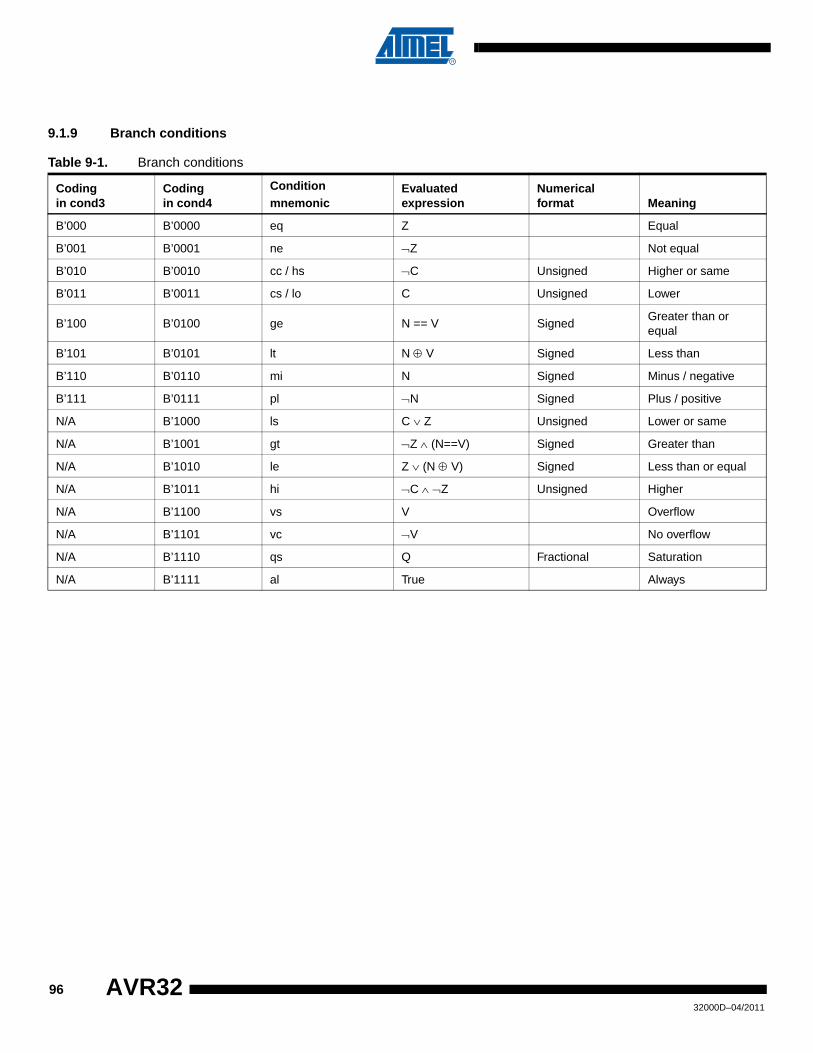
9.1.9 Branch conditions
Table 9-1. Branch conditions
Codingin cond3
Coding in cond4
Conditionmnemonic
Evaluatedexpression
Numericalformat Meaning
B’000 B’0000 eq Z Equal
B’001 B’0001 ne ¬Z Not equal
B’010 B’0010 cc / hs ¬C Unsigned Higher or same
B’011 B’0011 cs / lo C Unsigned Lower
B’100 B’0100 ge N == V SignedGreater than or equal
B’101 B’0101 lt N ⊕ V Signed Less than
B’110 B’0110 mi N Signed Minus / negative
B’111 B’0111 pl ¬N Signed Plus / positive
N/A B’1000 ls C ∨ Z Unsigned Lower or same
N/A B’1001 gt ¬Z ∧ (N==V) Signed Greater than
N/A B’1010 le Z ∨ (N ⊕ V) Signed Less than or equal
N/A B’1011 hi ¬C ∧ ¬Z Unsigned Higher
N/A B’1100 vs V Overflow
N/A B’1101 vc ¬V No overflow
N/A B’1110 qs Q Fractional Saturation
N/A B’1111 al True Always
9632000D–04/2011
AVR32
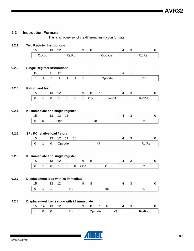
AVR32
9.2 Instruction FormatsThis is an overview of the different instruction formats.
9.2.1 Two Register Instructions
9.2.2 Single Register Instructions
9.2.3 Return and test
9.2.4 K8 immediate and single register
9.2.5 SP / PC relative load / store
9.2.6 K5 immediate and single register
9.2.7 Displacement load with k5 immediate
9.2.8 Displacement load / store with k3 immediate
Opcod Rs/Rp Opcode Rd/Rs
15 13 12 9 8 4 3 0
0 1 0 1 1 1 0 Opcode Rd
15 13 12 9 8 4 3 0
0 1 0 1 1 1 1 Opc cond4 Rs/Rd
15 13 12 9 8 7 4 3 0
0 0 1 Opc k8 Rd
15 13 12 11 4 3 0
0 1 0 Opcode k7 Rd/Rs
15 13 12 11 10 4 3 0
0 1 0 1 1 0 Opc k5 Rd
15 13 12 10 9 8 4 3 0
0 1 1 Rp k5 Rd
15 13 12 9 8 4 3 0
1 0 0 Rp Opcode k3 Rd/Rs
15 14 13 12 9 8 7 6 4 3 0
9732000D–04/2011

9.2.9 One register and a register pair
9.2.10 One register with k8 immediate and cond4
9.2.11 One register with bit addressing
9.2.12 Short branch
9.2.13 Relative jump and call
9.2.14 K8 and no register
9.2.15 Multiple registers (POPM)
9.2.16 Multiple registers (PUSHM)
9.2.17 Status register bit specification
1 0 1 Rp 1 0 0 Opc Rd/Rs Opc
15 13 12 9 8 6 5 4 3 1 0
1 1 1 Opcode 1 1 0 1 1 Rd
31 29 28 25 24 20 19 16
0 0 0 0 cond4 k8
15 12 11 8 7 0
1 0 1 Bit[4:1] Opcode Bit[0] Rd
15 13 12 9 8 5 4 3 0
1 1 0 0 k8 0 cond3
15 13 12 11 4 3 2 0
1 1 0 0 K10[7:0] 1 Opc K10[9:8]
15 13 12 11 4 3 2 1 0
1 1 0 1 k8/Label 0 0 0 Opc
15 12 11 4 3 1 0
1 1 0 1 PC LR 12 11 10 9-8 7-4 3-0 k 0 1 0
15 3 2 0
1 1 0 1 PC LR 12 11 10 9-8 7-4 3-0 0 0 1 1
15 13 12 11 4 3 0
1 1 0 1 0 Opcode Bit No 0 1 0 0
15 11 10 9 8 4 3 0
9832000D–04/2011
AVR32
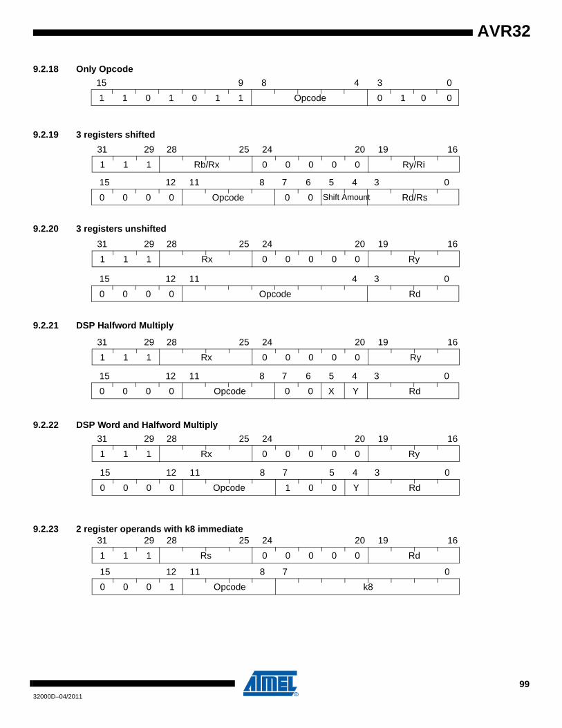
AVR32
9.2.18 Only Opcode
9.2.19 3 registers shifted
9.2.20 3 registers unshifted
9.2.21 DSP Halfword Multiply
9.2.22 DSP Word and Halfword Multiply
9.2.23 2 register operands with k8 immediate
1 1 0 1 0 1 1 Opcode 0 1 0 0
15 9 8 4 3 0
1 1 1 Rb/Rx 0 0 0 0 0 Ry/Ri
31 29 28 25 24 20 19 16
0 0 0 0 Opcode 0 0 Shift Amount Rd/Rs
15 12 11 8 7 6 5 4 3 0
1 1 1 Rx 0 0 0 0 0 Ry
31 29 28 25 24 20 19 16
0 0 0 0 Opcode Rd
15 12 11 4 3 0
1 1 1 Rx 0 0 0 0 0 Ry
31 29 28 25 24 20 19 16
0 0 0 0 Opcode 0 0 X Y Rd
15 12 11 8 7 6 5 4 3 0
1 1 1 Rx 0 0 0 0 0 Ry
31 29 28 25 24 20 19 16
0 0 0 0 Opcode 1 0 0 Y Rd
15 12 11 8 7 5 4 3 0
1 1 1 Rs 0 0 0 0 0 Rd
31 29 28 25 24 20 19 16
0 0 0 1 Opcode k8
15 12 11 8 7 0
9932000D–04/2011

9.2.24 2 register operands with k5 immediate
9.2.25 2 Registers with w5 and o5
9.2.26 Coprocessor 0 load and store
9.2.27 2 register operands
9.2.28 Register operand with K16
9.2.29 Cache operation
1 1 1 Rs 0 0 0 0 0 Rd
31 29 28 25 24 20 19 16
0 0 0 1 Opcode 0 0 0 k5
15 12 11 8 7 5 4 0
1 1 1 Rd 1 1 1 0 1 Rs
31 29 28 25 24 20 19 16
Opcode o5 w5
15 10 9 5 4 0
1 1 1 1 Opc 1 1 0 1 0 Rp
31 29 28 26 25 24 20 19 16
k12 [11:8] CRd/CRs k12[7:0]
15 13 12 11 8 7 6 0
1 1 1 Rs 0 0 0 0 0 Rd
31 29 28 25 24 20 19 16
0 0 0 1 Opcode 0 0 0 0 0 0 0 0
15 12 11 8 7 0
1 1 1 Opcode Rd/Rp
31 29 28 20 19 16
k16
15 0
1 1 1 1 1 0 0 0 0 0 1 Rp
31 20 19 16
Op5 k11
15 0
0
10032000D–04/2011
AVR32
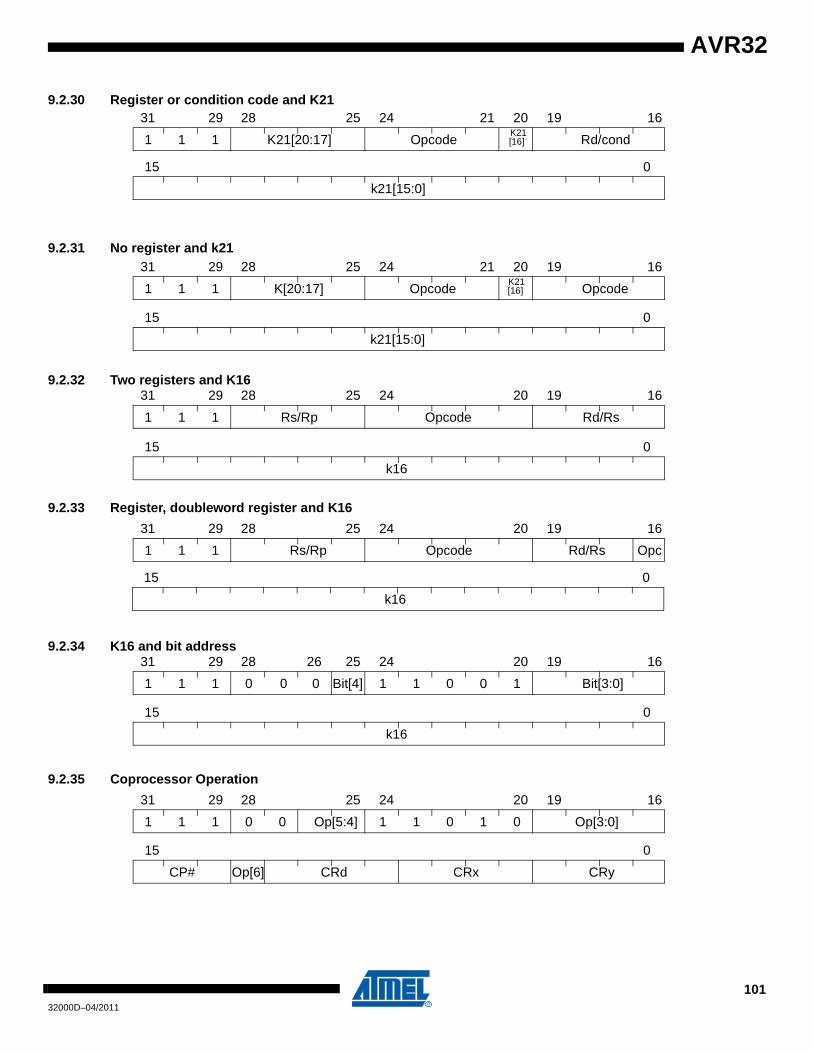
AVR32
9.2.30 Register or condition code and K21
9.2.31 No register and k21
9.2.32 Two registers and K16
9.2.33 Register, doubleword register and K16
9.2.34 K16 and bit address
9.2.35 Coprocessor Operation
1 1 1 K21[20:17] OpcodeK21
Rd/cond
31 29 28 25 24 21 20 19 16
k21[15:0]
15 0
[16]
1 1 1 K[20:17] OpcodeK21
Opcode
31 29 28 25 24 21 20 19 16
k21[15:0]
15 0
[16]
1 1 1 Rs/Rp Opcode Rd/Rs
31 29 28 25 24 20 19 16
k16
15 0
1 1 1 Rs/Rp Opcode Rd/Rs Opc
31 29 28 25 24 20 19 16
k16
15 0
1 1 1 0 0 Bit[4] 1 1 0 0 1 Bit[3:0]
31 29 28 26 25 24 20 19 16
k16
15 0
0
1 1 1 0 0 Op[5:4] 1 1 0 1 0 Op[3:0]
31 29 28 25 24 20 19 16
CP# Op[6] CRd CRx CRy
15 0
10132000D–04/2011

9.2.36 Coprocessor load and store
9.2.37 Coprocessor load and store multiple registers
9.2.38 Coprocessor load, store and move
9.2.39 Coprocessor load and store with indexed addressing
9.2.40 Register and system register
9.2.41 Sleep and sync
1 1 1 0 0 Opc 1 1 0 1 0 Rp
31 29 28 26 25 24 20 19 16
CP # Opc CRd/CRs k8
15 13 12 11 8 7 6 0
1
1 1 1 0 1 0 1 1 0 1 0 Rp
31 29 28 25 24 20 19 16
CP # ++/-- 0 OpcodeCR
14-
15 13 12 11 10 9 8 7 0
1
CR
13-CR
11-CR
9-8CR
7-6CR
5-4CR
3-2CR
1-0
1 1 1 0 1 1 1 1 0 1 0 Rd/Rs/Rp
31 29 28 25 24 20 19 16
CP# Opc CRs/CRd 0 Opc 0 0 0
15 13 12 11 8 7 6 4 3 0
1
0
1 1 1 0 1 1 1 1 0 1 0 Rp
31 29 28 25 24 20 19 17 16
CP# Opc CRs/CRd Opc k k i3
15 13 12 11 9 8 7 6 5 4 3 0
1
1 1 1 0 0 0 Opc 1 1 0 1 1 Rd/Rs
31 20 19 16
0 0 0 0 0 0 0 0 System Register Ad-
15 8 7 0
1 1 1 Opcode 1 1 0 1 1 0 0 0
31 29 28 25 24 20 19 16
0 0 0 0 0 0 0 0 Op8
15 8 7 0
0
10232000D–04/2011
AVR32
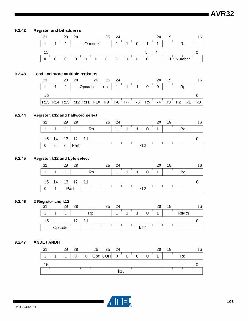
AVR32
9.2.42 Register and bit address
9.2.43 Load and store multiple registers
9.2.44 Register, k12 and halfword select
9.2.45 Register, k12 and byte select
9.2.46 2 Register and k12
9.2.47 ANDL / ANDH
1 1 1 Opcode 1 1 0 1 1 Rd
31 29 28 25 24 20 19 16
0 0 0 0 0 0 0 0 0 0 0 Bit Number
15 5 4 0
1 1 1 Opcode ++/-- 1 1 1 0 0 Rp
31 29 28 26 25 24 20 19 16
R15 R14 R13 R12 R11 R10 R9 R8 R7 R6 R5 R4 R3 R2 R1 R0
15 0
1 1 1 Rp 1 1 1 0 1 Rd
31 29 28 25 24 20 19 16
0 0 Part k12
15 14 13 12 11 0
0
1 1 1 Rp 1 1 1 0 1 Rd
31 29 28 25 24 20 19 16
0 1 Part k12
15 14 13 12 11 0
1 1 1 Rp 1 1 1 0 1 Rd/Rs
31 29 28 25 24 20 19 16
Opcode k12
15 12 11 0
1 1 1 0 0 Opc COH 0 0 0 0 1 Rd
31 29 28 26 25 24 20 19 16
k16
15 0
10332000D–04/2011
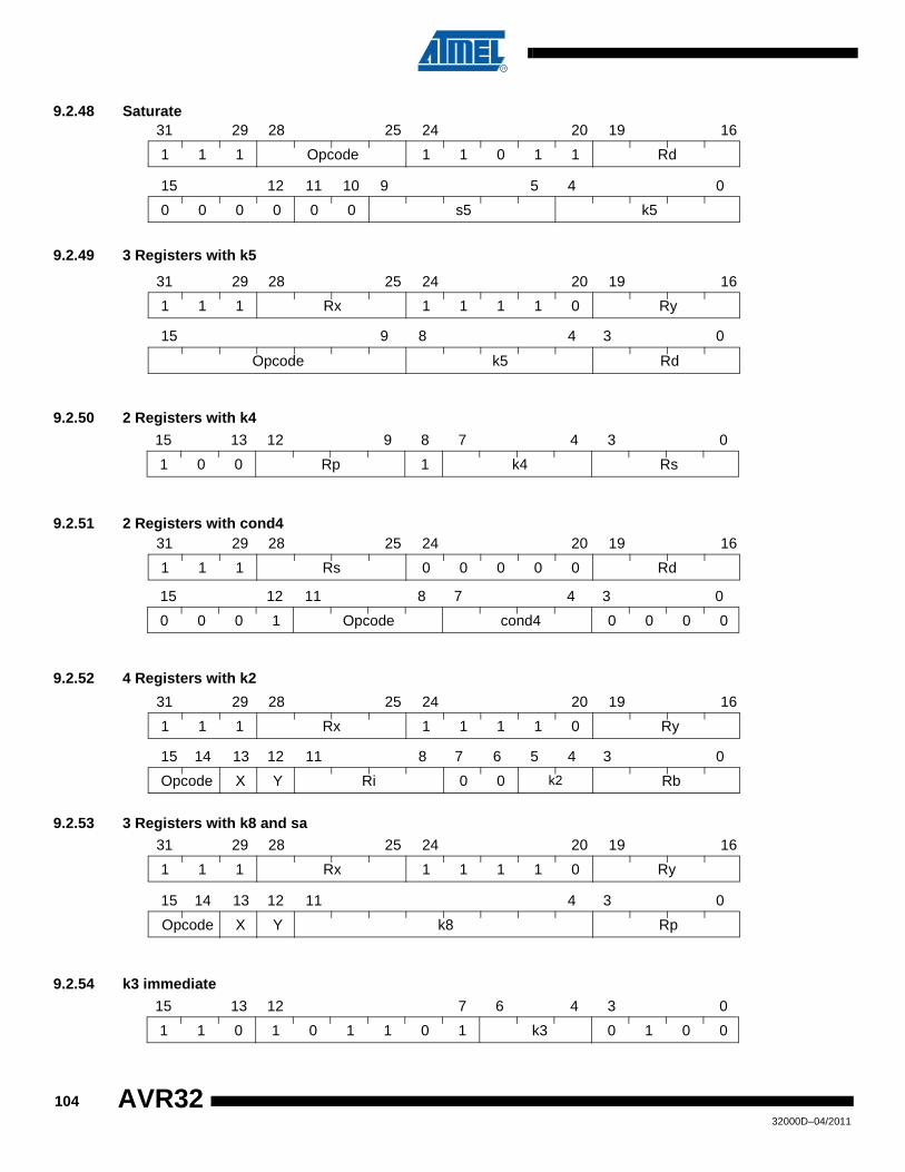
9.2.48 Saturate
9.2.49 3 Registers with k5
9.2.50 2 Registers with k4
9.2.51 2 Registers with cond4
9.2.52 4 Registers with k2
9.2.53 3 Registers with k8 and sa
9.2.54 k3 immediate
1 1 1 Opcode 1 1 0 1 1 Rd
31 29 28 25 24 20 19 16
0 0 0 0 0 0 s5 k5
15 12 11 10 9 5 4 0
1 1 1 Rx 1 1 1 1 0 Ry
31 29 28 25 24 20 19 16
Opcode k5 Rd
15 9 8 4 3 0
1 0 0 Rp 1 k4 Rs
15 13 12 9 8 7 4 3 0
1 1 1 Rs 0 0 0 0 0 Rd
31 29 28 25 24 20 19 16
0 0 0 1 Opcode cond4 0 0 0 0
15 12 11 8 7 4 3 0
1 1 1 Rx 1 1 1 1 0 Ry
31 29 28 25 24 20 19 16
Opcode X Y Ri 0 0 k2 Rb
15 14 13 12 11 8 7 6 5 4 3 0
1 1 1 Rx 1 1 1 1 0 Ry
31 29 28 25 24 20 19 16
Opcode X Y k8 Rp
15 14 13 12 11 4 3 0
1 1 0 1 0 1 1 0 1 k3 0 1 0 0
15 13 12 7 6 4 3 0
10432000D–04/2011
AVR32
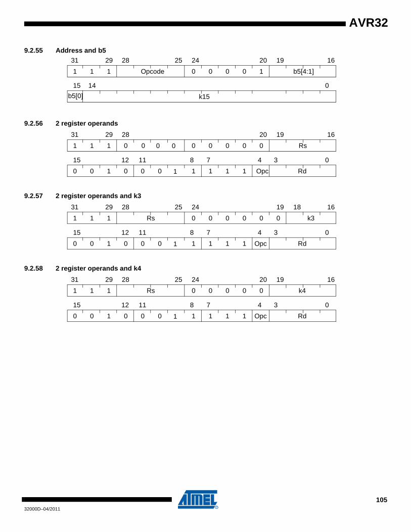
AVR32
9.2.55 Address and b5
9.2.56 2 register operands
9.2.57 2 register operands and k3
9.2.58 2 register operands and k4
1 1 1 Opcode 0 0 0 0 1 b5[4:1]
31 29 28 25 24 20 19 16
b5[0] k15
15 14 0
1 1 1 0 0 0 0 0 0 0 Rs
31 29 28 20 19 16
0 0 1 0 0 0 1 1 1 1 Opc Rd
15 12 11 8 7 4 3 0
0 0
1
1 1 1 Rs 0 0 0 0 0 0 k3
31 29 28 25 24 19 18 16
0 0 1 0 0 0 1 1 1 1 Opc Rd
15 12 11 8 7 4 3 0
1
1 1 1 Rs 0 0 0 0 0 k4
31 29 28 25 24 20 19 16
0 0 1 0 0 0 1 1 1 1 Opc Rd
15 12 11 8 7 4 3 0
1
10532000D–04/2011
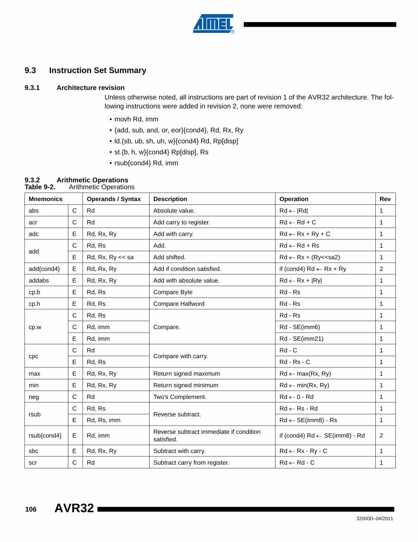
9.3 Instruction Set Summary
9.3.1 Architecture revisionUnless otherwise noted, all instructions are part of revision 1 of the AVR32 architecture. The fol-lowing instructions were added in revision 2, none were removed:
• movh Rd, imm
• {add, sub, and, or, eor}{cond4}, Rd, Rx, Ry
• ld.{sb, ub, sh, uh, w}{cond4} Rd, Rp[disp]
• st.{b, h, w}{cond4} Rp[disp], Rs
• rsub{cond4} Rd, imm
9.3.2 Arithmetic OperationsTable 9-2. Arithmetic Operations
Mnemonics Operands / Syntax Description Operation Rev
abs C Rd Absolute value. Rd ← |Rd| 1
acr C Rd Add carry to register. Rd ← Rd + C 1
adc E Rd, Rx, Ry Add with carry. Rd ← Rx + Ry + C 1
add C Rd, Rs Add. Rd ← Rd + Rs 1
E Rd, Rx, Ry << sa Add shifted. Rd ← Rx + (Ry<<sa2) 1
add{cond4} E Rd, Rx, Ry Add if condition satisfied. if (cond4) Rd ← Rx + Ry 2
addabs E Rd, Rx, Ry Add with absolute value. Rd ← Rx + |Ry| 1
cp.b E Rd, Rs Compare Byte Rd - Rs 1
cp.h E Rd, Rs Compare Halfword Rd - Rs 1
cp.w
C Rd, Rs
Compare.
Rd - Rs 1
C Rd, imm Rd - SE(imm6) 1
E Rd, imm Rd - SE(imm21) 1
cpcC Rd
Compare with carry.Rd - C 1
E Rd, Rs Rd - Rs - C 1
max E Rd, Rx, Ry Return signed maximum Rd ← max(Rx, Ry) 1
min E Rd, Rx, Ry Return signed minimum Rd ← min(Rx, Ry) 1
neg C Rd Two’s Complement. Rd ← 0 - Rd 1
rsubC Rd, Rs
Reverse subtract.Rd ← Rs - Rd 1
E Rd, Rs, imm Rd ← SE(imm8) - Rs 1
rsub{cond4} E Rd, immReverse subtract immediate if condition satisfied.
if (cond4) Rd ← SE(imm8) - Rd 2
sbc E Rd, Rx, Ry Subtract with carry. Rd ← Rx - Ry - C 1
scr C Rd Subtract carry from register. Rd ← Rd - C 1
10632000D–04/2011
AVR32
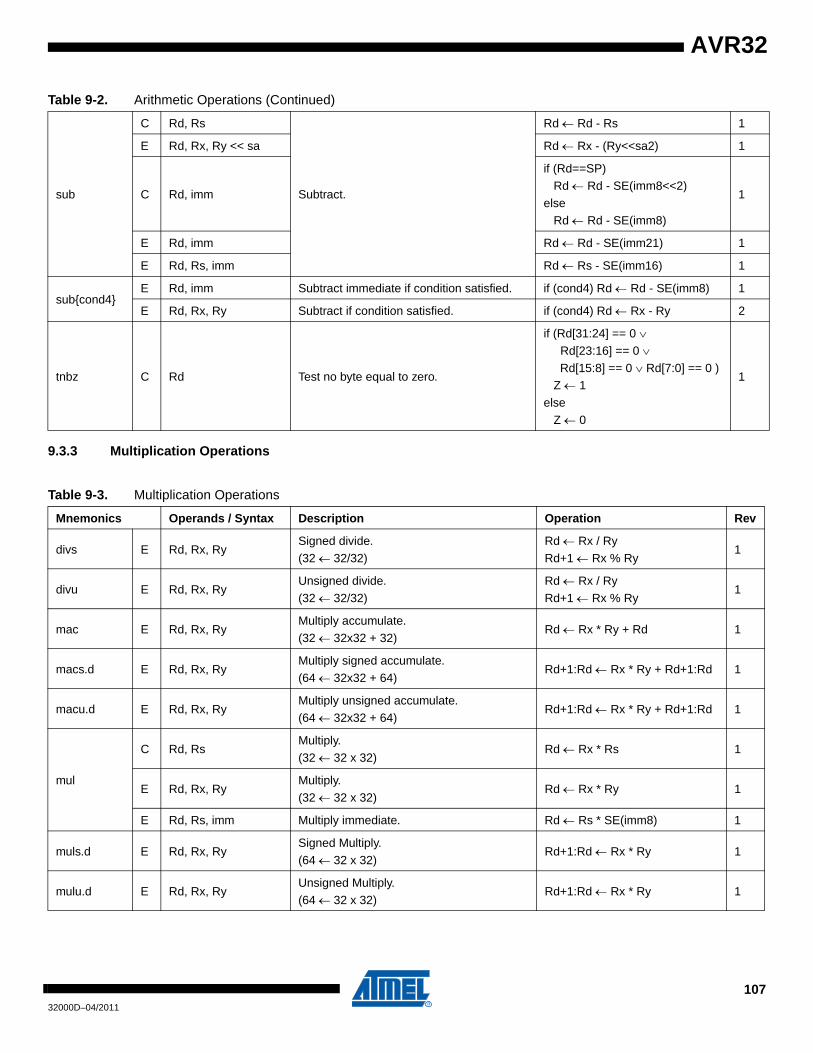
AVR32
9.3.3 Multiplication Operations
sub
C Rd, Rs
Subtract.
Rd ← Rd - Rs 1
E Rd, Rx, Ry << sa Rd ← Rx - (Ry<<sa2) 1
C Rd, imm
if (Rd==SP)
Rd ← Rd - SE(imm8<<2)
else
Rd ← Rd - SE(imm8)
1
E Rd, imm Rd ← Rd - SE(imm21) 1
E Rd, Rs, imm Rd ← Rs - SE(imm16) 1
sub{cond4}E Rd, imm Subtract immediate if condition satisfied. if (cond4) Rd ← Rd - SE(imm8) 1
E Rd, Rx, Ry Subtract if condition satisfied. if (cond4) Rd ← Rx - Ry 2
tnbz C Rd Test no byte equal to zero.
if (Rd[31:24] == 0 ∨
Rd[23:16] == 0 ∨ Rd[15:8] == 0 ∨ Rd[7:0] == 0 ) Z ← 1
else
Z ← 0
1
Table 9-2. Arithmetic Operations (Continued)
Table 9-3. Multiplication Operations
Mnemonics Operands / Syntax Description Operation Rev
divs E Rd, Rx, RySigned divide.
(32 ← 32/32)
Rd ← Rx / Ry
Rd+1 ← Rx % Ry1
divu E Rd, Rx, RyUnsigned divide.
(32 ← 32/32)
Rd ← Rx / Ry
Rd+1 ← Rx % Ry1
mac E Rd, Rx, RyMultiply accumulate.
(32 ← 32x32 + 32)Rd ← Rx * Ry + Rd 1
macs.d E Rd, Rx, RyMultiply signed accumulate.
(64 ← 32x32 + 64)Rd+1:Rd ← Rx * Ry + Rd+1:Rd 1
macu.d E Rd, Rx, RyMultiply unsigned accumulate.
(64 ← 32x32 + 64)Rd+1:Rd ← Rx * Ry + Rd+1:Rd 1
mul
C Rd, RsMultiply.
(32 ← 32 x 32)Rd ← Rx * Rs 1
E Rd, Rx, RyMultiply.
(32 ← 32 x 32)Rd ← Rx * Ry 1
E Rd, Rs, imm Multiply immediate. Rd ← Rs * SE(imm8) 1
muls.d E Rd, Rx, RySigned Multiply.
(64 ← 32 x 32)Rd+1:Rd ← Rx * Ry 1
mulu.d E Rd, Rx, RyUnsigned Multiply.
(64 ← 32 x 32)Rd+1:Rd ← Rx * Ry 1
10732000D–04/2011

9.3.4 DSP Operations
Table 9-4. DSP Operations
Mnemonics Operands / Syntax Description Operation Rev
addhh.w ERd, Rx:<part>, Ry:<part>
Add signed halfwords.
(32 ← 16 +16)Rd ← SE(Rx:<part>) + SE(Ry:<part>)
1
machh.d ERd, Rx:<part>, Ry:<part>
Multiply signed halfwords and accumulate.
(48 ← 16x16 + 48)
Rd+1:Rd ← Rx:<part> * Ry:<part> + Rd+1:Rd
1
machh.w ERd, Rx:<part>, Ry:<part>
Multiply signed halfwords and accumulate.(32 ← 16x16 + 32)
Rd ← Rx:<part> * Ry:<part> + Rd 1
macwh.d E Rd, Rx, Ry:<part>Multiply signed word and halfword and accumulate.
(48 ← 32x16 + 48)
Rd+1:Rd ← ((Rx * Ry:<part>) <<16) + Rd+1:Rd
1
mulhh.w ERd, Rx:<part>, Ry:<part>
Signed Multiply of halfwords.
(32 ← 16 x 16)Rd ← Rx:<part> * Ry:<part> 1
mulwh.d E Rd, Rx, Ry:<part>Unsigned Multiply, word and halfword.
48 ← (32 x 16)Rd+1:Rd ← ((Rx * Ry:<part>) <<16)
1
mulnhh.w ERd, Rx:<part>, Ry:<part>
Signed Multiply of halfwords.
(32 ← 16 x 16)Rd ← Rx:<part> * (- Ry:<part>) 1
mulnwh.d E Rd, Rx, Ry:<part>Signed Multiply, word and negated halfword.
48 ← (32 x 16)
Rd+1:Rd ← ((Rx * (- Ry:<part>)) << 16)
1
satadd.h E Rd, Rx, Ry Saturated add halfwords.Rd ← SE(Sat(Rx[15:0] + Ry[15:0]))
1
satadd.w E Rd, Rx, Ry Saturated add. Rd ← Sat(Rx + Ry) 1
satsub.h E Rd, Rx, Ry Saturated subtract halfwords. Rd ← SE(Sat(Rx[15:0] - Ry[15:0])) 1
satsub.wE Rd, Rx, Ry
Saturated subtract.Rd ← Sat(Rx - Ry) 1
E Rd, Rs, imm Rd ← Sat(Rs - SE(imm16) ) 1
satrnds E Rd >> sa, bpSigned saturate from bit given by sa5 after a right shift with rounding of bp5 bit positions.
Rd ← Sat(Round((Rd >> sa5)), bp5)
1
satrndu E Rd >> sa, bpUnsigned saturate from bit given by sa5 after a right shift with rounding of bp5 bit positions.
Rd ← Sat(Round((Rd >> sa5)), bp5)
1
sats E Rd >> sa, bpSigned saturate from bit given by sa5 after a right shift of bp5 bit positions.
Rd ← Sat((Rd >> sa5), bp5) 1
satu E Rd >> sa, bpUnsigned saturate from bit given by sa5 after a right shift of bp5 bit positions.
Rd ← Sat((Rd >> sa5),bp5) 1
subhh.w ERd, Rx:<part>, Ry:<part>
Subtract signed halfwords.
(32 ← 16 -16)Rd ← SE(Rx:<part>) - SE(Ry:<part>)
1
10832000D–04/2011
AVR32
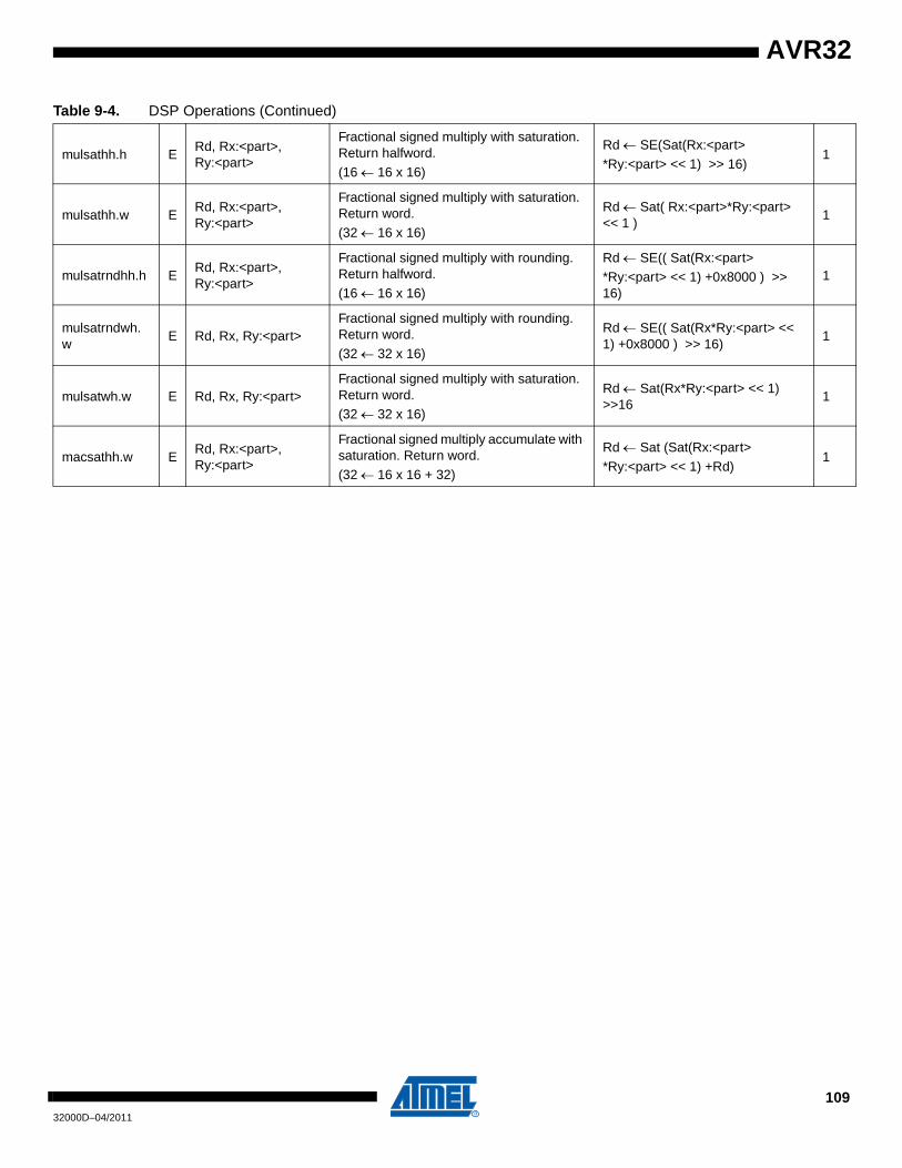
AVR32
mulsathh.h ERd, Rx:<part>, Ry:<part>
Fractional signed multiply with saturation. Return halfword.
(16 ← 16 x 16)
Rd ← SE(Sat(Rx:<part>
*Ry:<part> << 1) >> 16)1
mulsathh.w ERd, Rx:<part>, Ry:<part>
Fractional signed multiply with saturation. Return word.
(32 ← 16 x 16)
Rd ← Sat( Rx:<part>*Ry:<part> << 1 )
1
mulsatrndhh.h ERd, Rx:<part>, Ry:<part>
Fractional signed multiply with rounding. Return halfword.
(16 ← 16 x 16)
Rd ← SE(( Sat(Rx:<part>*Ry:<part> << 1) +0x8000 ) >> 16)
1
mulsatrndwh.w
E Rd, Rx, Ry:<part>Fractional signed multiply with rounding. Return word.
(32 ← 32 x 16)
Rd ← SE(( Sat(Rx*Ry:<part> << 1) +0x8000 ) >> 16)
1
mulsatwh.w E Rd, Rx, Ry:<part>Fractional signed multiply with saturation. Return word.(32 ← 32 x 16)
Rd ← Sat(Rx*Ry:<part> << 1) >>16
1
macsathh.w ERd, Rx:<part>, Ry:<part>
Fractional signed multiply accumulate with saturation. Return word.
(32 ← 16 x 16 + 32)
Rd ← Sat (Sat(Rx:<part>
*Ry:<part> << 1) +Rd)1
Table 9-4. DSP Operations (Continued)
10932000D–04/2011
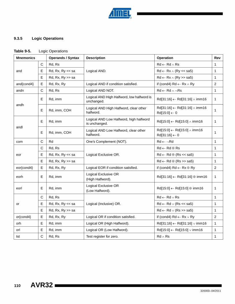
9.3.5 Logic Operations
Table 9-5. Logic Operations
Mnemonics Operands / Syntax Description Operation Rev
and
C Rd, Rs
Logical AND.
Rd ← Rd ∧ Rs 1
E Rd, Rx, Ry << sa Rd ← Rx ∧ (Ry << sa5) 1
E Rd, Rx, Ry >> sa Rd ← Rx ∧ (Ry >> sa5) 1
and{cond4} E Rd, Rx, Ry Logical AND if condition satisfied. if (cond4) Rd ← Rx ∧ Ry 2
andn C Rd, Rs Logical AND NOT. Rd ← Rd ∧ ¬Rs 1
andh
E Rd, immLogical AND High Halfword, low halfword is unchanged.
Rd[31:16] ← Rd[31:16] ∧ imm16 1
E Rd, imm, COHLogical AND High Halfword, clear other halfword.
Rd[31:16] ← Rd[31:16] ∧ imm16
Rd[15:0] ← 01
andl
E Rd, immLogical AND Low Halfword, high halfword is unchanged.
Rd[15:0] ← Rd[15:0] ∧ imm16 1
E Rd, imm, COHLogical AND Low Halfword, clear other halfword.
Rd[15:0] ← Rd[15:0] ∧ imm16
Rd[31:16] ← 01
com C Rd One’s Complement (NOT). Rd ← ¬Rd 1
eor
C Rd, Rs
Logical Exclusive OR.
Rd ← Rd ⊕ Rs 1
E Rd, Rx, Ry << sa Rd ← Rd ⊕ (Rs << sa5) 1
E Rd, Rx, Ry >> sa Rd ← Rd ⊕ (Rs >> sa5) 1
eor{cond4} E Rd, Rx, Ry Logical EOR if condition satisfied. if (cond4) Rd ← Rx ⊕ Ry 2
eorh E Rd, immLogical Exclusive OR (High Halfword).
Rd[31:16] ← Rd[31:16] ⊕ imm16 1
eorl E Rd, immLogical Exclusive OR (Low Halfword).
Rd[15:0] ← Rd[15:0] ⊕ imm16 1
or
C Rd, Rs
Logical (Inclusive) OR.
Rd ← Rd ∨ Rs 1
E Rd, Rx, Ry << sa Rd ← Rd ∨ (Rs << sa5) 1
E Rd, Rx, Ry >> sa Rd ← Rd ∨ (Rs >> sa5) 1
or{cond4} E Rd, Rx, Ry Logical OR if condition satisfied. if (cond4) Rd ← Rx ∨ Ry 2
orh E Rd, imm Logical OR (High Halfword). Rd[31:16] ← Rd[31:16] ∨ imm16 1
orl E Rd, imm Logical OR (Low Halfword). Rd[15:0] ← Rd[15:0] ∨ imm16 1
tst C Rd, Rs Test register for zero. Rd ∧ Rs 1
11032000D–04/2011
AVR32
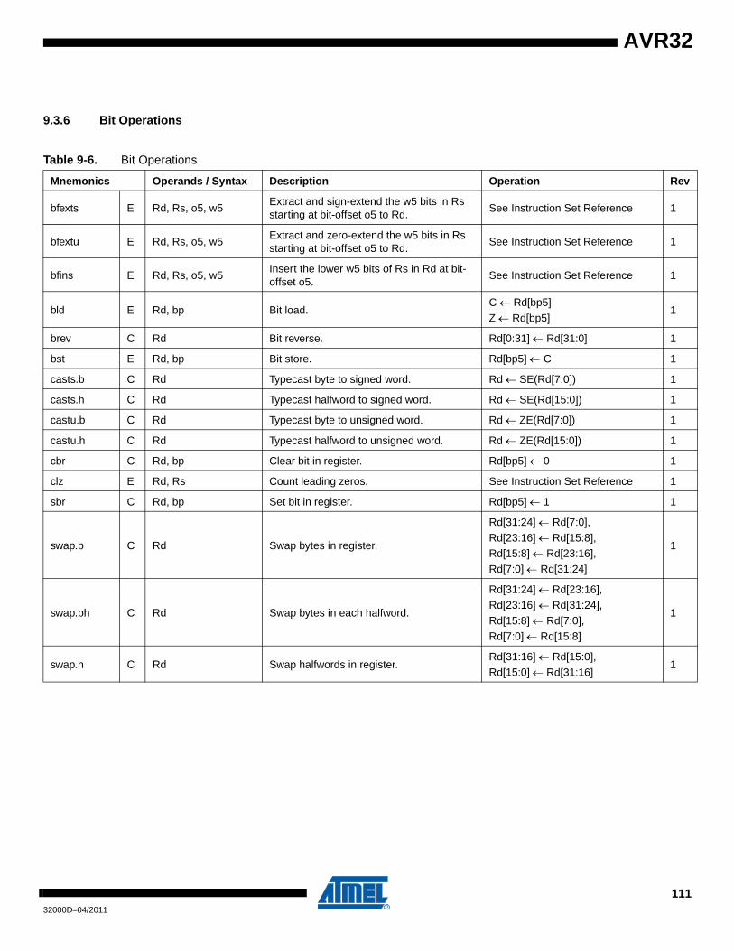
AVR32
9.3.6 Bit Operations
Table 9-6. Bit Operations
Mnemonics Operands / Syntax Description Operation Rev
bfexts E Rd, Rs, o5, w5Extract and sign-extend the w5 bits in Rs starting at bit-offset o5 to Rd.
See Instruction Set Reference 1
bfextu E Rd, Rs, o5, w5Extract and zero-extend the w5 bits in Rs starting at bit-offset o5 to Rd.
See Instruction Set Reference 1
bfins E Rd, Rs, o5, w5Insert the lower w5 bits of Rs in Rd at bit-offset o5.
See Instruction Set Reference 1
bld E Rd, bp Bit load.C ← Rd[bp5]
Z ← Rd[bp5]1
brev C Rd Bit reverse. Rd[0:31] ← Rd[31:0] 1
bst E Rd, bp Bit store. Rd[bp5] ← C 1
casts.b C Rd Typecast byte to signed word. Rd ← SE(Rd[7:0]) 1
casts.h C Rd Typecast halfword to signed word. Rd ← SE(Rd[15:0]) 1
castu.b C Rd Typecast byte to unsigned word. Rd ← ZE(Rd[7:0]) 1
castu.h C Rd Typecast halfword to unsigned word. Rd ← ZE(Rd[15:0]) 1
cbr C Rd, bp Clear bit in register. Rd[bp5] ← 0 1
clz E Rd, Rs Count leading zeros. See Instruction Set Reference 1
sbr C Rd, bp Set bit in register. Rd[bp5] ← 1 1
swap.b C Rd Swap bytes in register.
Rd[31:24] ← Rd[7:0],
Rd[23:16] ← Rd[15:8],Rd[15:8] ← Rd[23:16],
Rd[7:0] ← Rd[31:24]
1
swap.bh C Rd Swap bytes in each halfword.
Rd[31:24] ← Rd[23:16],
Rd[23:16] ← Rd[31:24],
Rd[15:8] ← Rd[7:0],Rd[7:0] ← Rd[15:8]
1
swap.h C Rd Swap halfwords in register. Rd[31:16] ← Rd[15:0],Rd[15:0] ← Rd[31:16]
1
11132000D–04/2011

9.3.7 Shift Operations
Table 9-7. Operations
Mnemonics Operands / Syntax Description Operation Rev
asr
E Rd, Rx, Ry
Arithmetic shift right (signed) . See Instruction Set Reference
1
E Rd, Rs, sa 1
C Rd, sa 1
lsl
E Rd, Rx, Ry
Logical shift left. See Instruction Set Reference
1
E Rd, Rs, sa 1
C Rd, sa 1
lsr
E Rd, Rx, Ry
Logical shift right. See Instruction Set Reference
1
E Rd, Rs, sa 1
C Rd, sa 1
rol C Rd Rotate left through carry. See Instruction Set Reference 1
ror C Rd Rotate right through carry. See Instruction Set Reference 1
11232000D–04/2011
AVR32
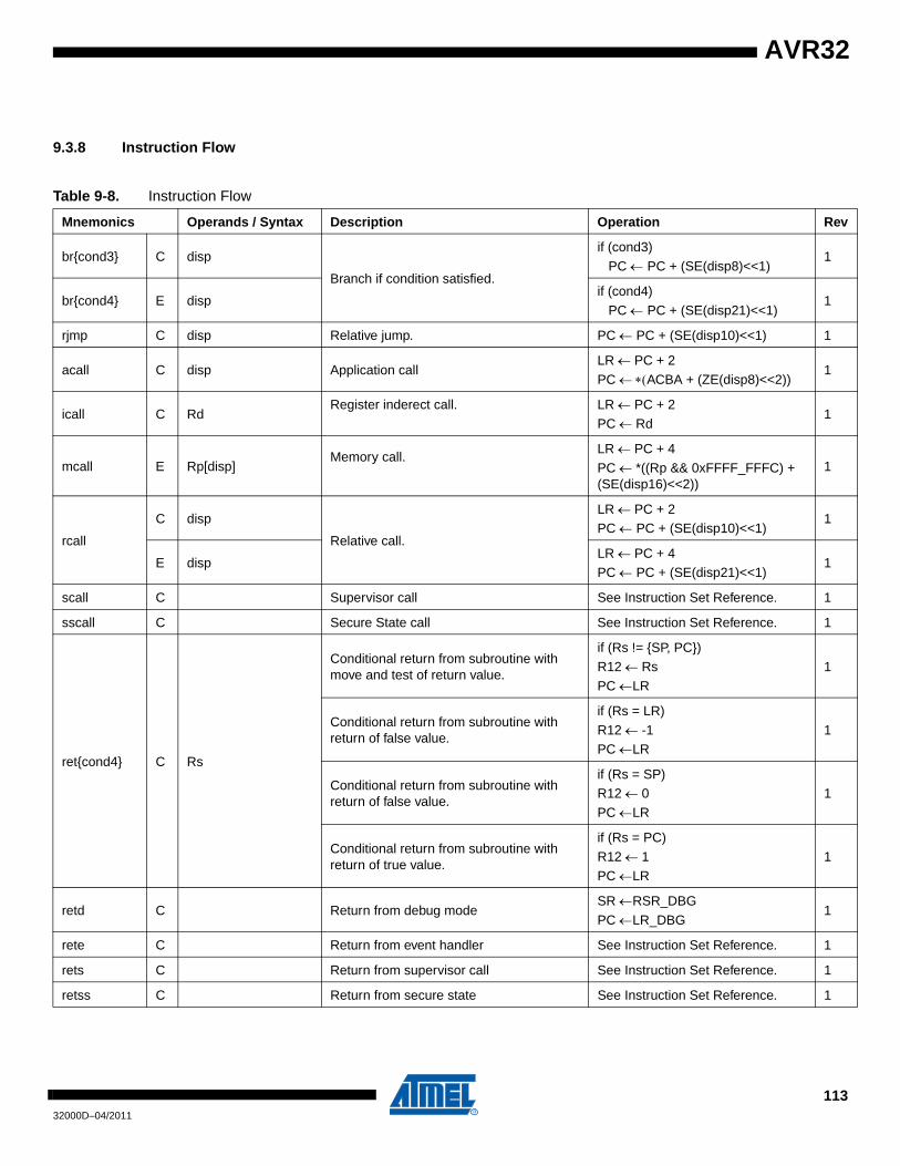
AVR32
9.3.8 Instruction Flow
Table 9-8. Instruction Flow
Mnemonics Operands / Syntax Description Operation Rev
br{cond3} C disp
Branch if condition satisfied.
if (cond3)
PC ← PC + (SE(disp8)<<1)1
br{cond4} E dispif (cond4)
PC ← PC + (SE(disp21)<<1)1
rjmp C disp Relative jump. PC ← PC + (SE(disp10)<<1) 1
acall C disp Application callLR ← PC + 2
PC ← ∗(ACBA + (ZE(disp8)<<2))1
icall C RdRegister inderect call. LR ← PC + 2
PC ← Rd1
mcall E Rp[disp]Memory call.
LR ← PC + 4
PC ← *((Rp && 0xFFFF_FFFC) + (SE(disp16)<<2))
1
rcall
C disp
Relative call.
LR ← PC + 2PC ← PC + (SE(disp10)<<1)
1
E dispLR ← PC + 4PC ← PC + (SE(disp21)<<1)
1
scall C Supervisor call See Instruction Set Reference. 1
sscall C Secure State call See Instruction Set Reference. 1
ret{cond4} C Rs
Conditional return from subroutine with move and test of return value.
if (Rs != {SP, PC})
R12 ← Rs
PC ←LR
1
Conditional return from subroutine with return of false value.
if (Rs = LR)
R12 ← -1PC ←LR
1
Conditional return from subroutine with return of false value.
if (Rs = SP)R12 ← 0PC ←LR
1
Conditional return from subroutine with return of true value.
if (Rs = PC)
R12 ← 1PC ←LR
1
retd C Return from debug modeSR ←RSR_DBG
PC ←LR_DBG1
rete C Return from event handler See Instruction Set Reference. 1
rets C Return from supervisor call See Instruction Set Reference. 1
retss C Return from secure state See Instruction Set Reference. 1
11332000D–04/2011

9.3.9 Data Transfer
9.3.9.1 Move/Load Immediate operations
9.3.9.2 Load/Store operations
Table 9-9. Move/Load Immediate Operations
Mnemonics Operands / Syntax Description Operation Rev
mov
C Rd, immLoad immediate into register.
Rd ← SE(imm8) 1
E Rd, imm Rd ← SE(imm21) 1
C Rd, Rs Copy register. Rd ← Rs 1
mov{cond4}
E Rd, Rs Copy register if condition is true if (cond4) Rd ← Rs 1
E Rd, immLoad immediate into register if condition is true
if (cond4) Rd ← SE(imm8) 1
movh E Rd, immLoad immediate into high halfword of register.
Rd ← imm16<<16 2
Table 9-10. Load/Store Operations
Mnemonics Operands / Syntax Description Operation Rev
ld.ub
C Rd, Rp++ Load unsigned byte with post-increment. Rd ← ZE(*(Rp++)) 1
C Rd, --Rp Load unsigned byte with pre-decrement. Rd ← ZE(*(--Rp)) 1
C Rd, Rp[disp]Load unsigned byte with displacement.
Rd ← ZE(*(Rp+ZE(disp3))) 1
E Rd, Rp[disp] Rd ← ZE(*(Rp+SE(disp16))) 1
E Rd, Rb[Ri<<sa] Indexed Load unsigned byte. Rd ← ZE(*(Rb+(Ri << sa2))) 1
ld.ub{cond4} E Rd, Rp[disp]Load unsigned byte with displacement if condition satisfied.
if {cond4} Rd ← ZE(*(Rp+ZE(disp9)))
2
ld.sbE Rd, Rp[disp] Load signed byte with displacement. Rd ← SE(*(Rp+SE(disp16))) 1
E Rd, Rb[Ri<<sa] Indexed Load signed byte. Rd ← SE(*(Rb+(Ri << sa2))) 1
ld.sb{cond4} E Rd, Rp[disp]Load signed byte with displacement if condition satisfied.
if {cond4}
Rd ← SE(*(Rp+ZE(disp9)))2
ld.uh
C Rd, Rp++Load unsigned halfword with post-increment.
Rd ← ZE(*(Rp++)) 1
C Rd, --RpLoad unsigned halfword with pre-decrement.
Rd ← ZE(*(--Rp)) 1
C Rd, Rp[disp] Load unsigned halfword with displacement.
Rd ← ZE(*(Rp+(ZE(disp3)<<1))) 1
E Rd, Rp[disp] Rd ← ZE(*(Rp+(SE(disp16)))) 1
E Rd, Rb[Ri<<sa] Indexed Load unsigned halfword. Rd ← ZE(*(Rb+(Ri << sa2))) 1
ld.uh{cond4} E Rd, Rp[disp]Load unsigned halfword with displacement if condition satisfied.
if {cond4}
Rd ← ZE(*(Rp+ZE(disp9<<1)))2
11432000D–04/2011
AVR32

AVR32
ld.sh
C Rd, Rp++Load signed halfword with post-increment.
Rd ← SE(*(Rp++)) 1
C Rd, --Rp Load signed halfword with pre-decrement. Rd ← SE(*(--Rp)) 1
C Rd, Rp[disp]Load signed halfword with displacement.
Rd ← SE(*(Rp+(ZE(disp3)<<1))) 1
E Rd, Rp[disp] Rd ← SE(*(Rp+(SE(disp16)))) 1
E Rd, Rb[Ri<<sa] Indexed Load signed halfword. Rd ← SE(*(Rb+(Ri << sa2))) 1
ld.sh{cond4} E Rd, Rp[disp]Load signed halfword with displacement if condition satisfied.
if {cond4}
Rd ← SE(*(Rp+ZE(disp9<<1)))2
ld.w
C Rd, Rp++ Load word with post-increment. Rd ← *(Rp++) 1
C Rd, --Rp Load word with pre-decrement. Rd ← *(--Rp) 1
C Rd, Rp[disp]Load word with displacement.
Rd ← *(Rp+(ZE(disp5)<<2)) 1
E Rd, Rp[disp] Rd ← *(Rp+(SE(disp16))) 1
E Rd, Rb[Ri<<sa] Indexed Load word. Rd ← *(Rb+(Ri << sa2)) 1
ERd, Rb[Ri:<part> << 2]
Load word with extracted index into Rd. Rd ← *(Rb+(Ri:<part> << 2)) 1
ld.w{cond4} E Rd, Rp[disp]Load word with displacement if condition satisfied.
if {cond4}
Rd ← *(Rp+ZE(disp9<<2))2
ld.d
C Rd, Rp++ Load doubleword with post-increment. Rd+1:Rd ← (*(Rp++)) 1
C Rd, --Rp Load doubleword with pre-decrement. Rd+1:Rd ← (*(--Rp)) 1
C Rd, Rp Load doubleword. Rd+1:Rd ← *(Rp) 1
E Rd, Rp[disp] Load double with displacement. Rd+1:Rd ← *(Rp+SE(disp16)) 1
E Rd, Rb[Ri<<sa] Indexed Load double. Rd+1:Rd ← *(Rb+(Ri << sa2)) 1
ldins.b E Rd:<part>, Rp[disp]Load byte with displacement and insert at specified byte location in Rd.
Rd:<part>← *(Rp+(SE(disp12))) 1
ldins.h E Rd:<part>, Rp[disp]Load halfword with displacement and insert at specified halfword location in Rd.
Rd:<part> ← *(Rp+(SE(disp12)<<1))
1
ldswp.sh E
Rd, Rp[disp]
Load halfword with displacement, swap bytes and sign-extend
Temp ← *(Rp+(SE(disp12) << 1)
Rd ← SE(Temp[7:0], Temp[15:8])1
ldswp.uh ELoad halfword with displacement, swap bytes and zero-extend
Temp ← *(Rp+(SE(disp12) << 1)
Rd ← ZE(Temp[7:0], Temp[15:8])1
ldswp.w ELoad word with displacement and swap bytes.
Temp ← *(Rp+(SE(disp12) << 2)
Rd[31:24] ← Temp[7:0],
Rd[23:16] ← Temp[15:8],Rd[15:8] ← Temp[23:16],
Rd[7:0] ← Temp[31:24]
1
lddpc C Rd, PC[disp] Load with displacement from PC.Rd ← *((PC && 0xFFFF_FFFC) +(ZE(disp7)<<2))
1
lddsp C Rd, SP[disp] Load with displacement from SP.Rd ← *((SP && 0xFFFF_FFFC) +(ZE(disp7)<<2))
1
Table 9-10. Load/Store Operations (Continued)
11532000D–04/2011
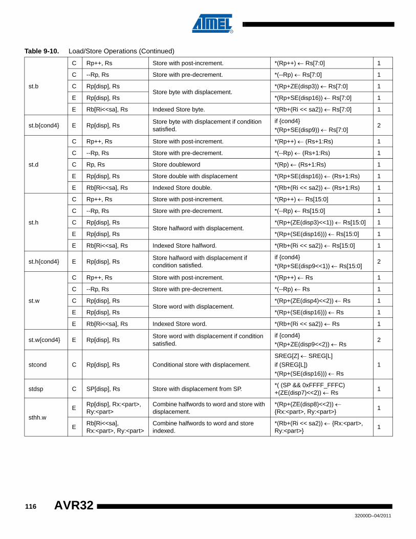
st.b
C Rp++, Rs Store with post-increment. *(Rp++) ← Rs[7:0] 1
C --Rp, Rs Store with pre-decrement. *(--Rp) ← Rs[7:0] 1
C Rp[disp], RsStore byte with displacement.
*(Rp+ZE(disp3)) ← Rs[7:0] 1
E Rp[disp], Rs *(Rp+SE(disp16)) ← Rs[7:0] 1
E Rb[Ri<<sa], Rs Indexed Store byte. *(Rb+(Ri << sa2)) ← Rs[7:0] 1
st.b{cond4} E Rp[disp], RsStore byte with displacement if condition satisfied.
if {cond4} *(Rp+SE(disp9)) ← Rs[7:0]
2
st.d
C Rp++, Rs Store with post-increment. *(Rp++) ← (Rs+1:Rs) 1
C --Rp, Rs Store with pre-decrement. *(--Rp) ← (Rs+1:Rs) 1
C Rp, Rs Store doubleword *(Rp) ← (Rs+1:Rs) 1
E Rp[disp], Rs Store double with displacement *(Rp+SE(disp16)) ← (Rs+1:Rs) 1
E Rb[Ri<<sa], Rs Indexed Store double. *(Rb+(Ri << sa2)) ← (Rs+1:Rs) 1
st.h
C Rp++, Rs Store with post-increment. *(Rp++) ← Rs[15:0] 1
C --Rp, Rs Store with pre-decrement. *(--Rp) ← Rs[15:0] 1
C Rp[disp], RsStore halfword with displacement.
*(Rp+(ZE(disp3)<<1)) ← Rs[15:0] 1
E Rp[disp], Rs *(Rp+(SE(disp16))) ← Rs[15:0] 1
E Rb[Ri<<sa], Rs Indexed Store halfword. *(Rb+(Ri << sa2)) ← Rs[15:0] 1
st.h{cond4} E Rp[disp], RsStore halfword with displacement if condition satisfied.
if {cond4}
*(Rp+SE(disp9<<1)) ← Rs[15:0]2
st.w
C Rp++, Rs Store with post-increment. *(Rp++) ← Rs 1
C --Rp, Rs Store with pre-decrement. *(--Rp) ← Rs 1
C Rp[disp], RsStore word with displacement.
*(Rp+(ZE(disp4)<<2)) ← Rs 1
E Rp[disp], Rs *(Rp+(SE(disp16))) ← Rs 1
E Rb[Ri<<sa], Rs Indexed Store word. *(Rb+(Ri << sa2)) ← Rs 1
st.w{cond4} E Rp[disp], RsStore word with displacement if condition satisfied.
if {cond4} *(Rp+ZE(disp9<<2)) ← Rs
2
stcond C Rp[disp], Rs Conditional store with displacement.SREG[Z] ← SREG[L]if (SREG[L])
*(Rp+(SE(disp16))) ← Rs
1
stdsp C SP[disp], Rs Store with displacement from SP.*( (SP && 0xFFFF_FFFC) +(ZE(disp7)<<2)) ← Rs
1
sthh.w
ERp[disp], Rx:<part>, Ry:<part>
Combine halfwords to word and store with displacement.
*(Rp+(ZE(disp8)<<2)) ← {Rx:<part>, Ry:<part>}
1
ERb[Ri<<sa], Rx:<part>, Ry:<part>
Combine halfwords to word and store indexed.
*(Rb+(Ri << sa2)) ← {Rx:<part>, Ry:<part>}
1
Table 9-10. Load/Store Operations (Continued)
11632000D–04/2011
AVR32
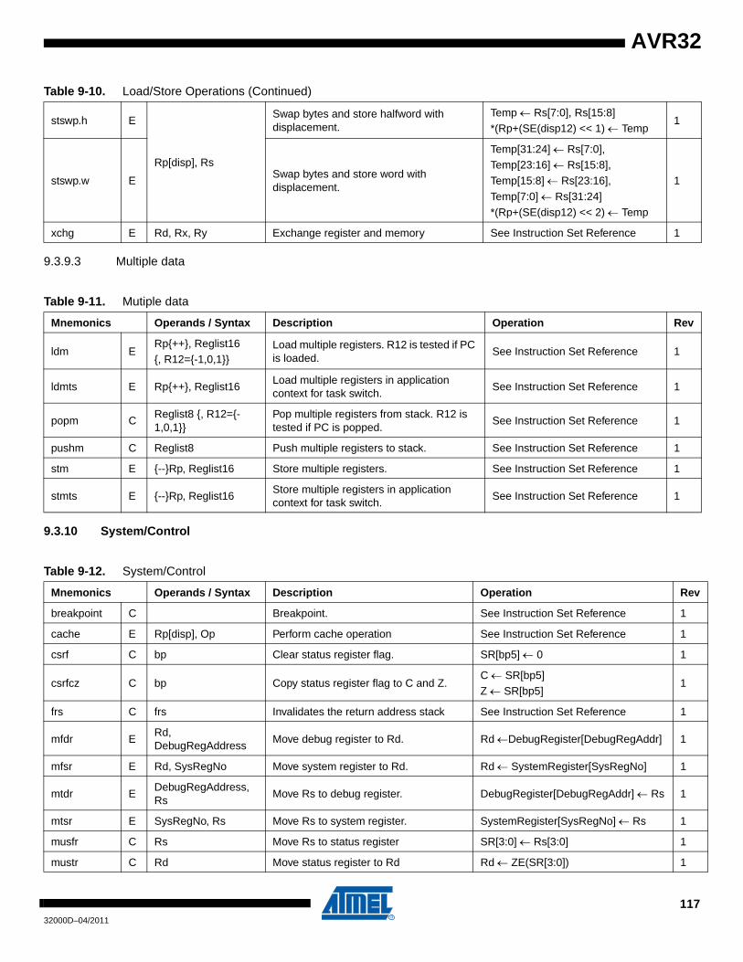
AVR32
9.3.9.3 Multiple data
9.3.10 System/Control
stswp.h E
Rp[disp], Rs
Swap bytes and store halfword with displacement.
Temp ← Rs[7:0], Rs[15:8]*(Rp+(SE(disp12) << 1) ← Temp
1
stswp.w ESwap bytes and store word with displacement.
Temp[31:24] ← Rs[7:0],Temp[23:16] ← Rs[15:8],
Temp[15:8] ← Rs[23:16],
Temp[7:0] ← Rs[31:24]
*(Rp+(SE(disp12) << 2) ← Temp
1
xchg E Rd, Rx, Ry Exchange register and memory See Instruction Set Reference 1
Table 9-10. Load/Store Operations (Continued)
Table 9-11. Mutiple data
Mnemonics Operands / Syntax Description Operation Rev
ldm ERp{++}, Reglist16 {, R12={-1,0,1}}
Load multiple registers. R12 is tested if PC is loaded.
See Instruction Set Reference 1
ldmts E Rp{++}, Reglist16Load multiple registers in application context for task switch.
See Instruction Set Reference 1
popm CReglist8 {, R12={-1,0,1}}
Pop multiple registers from stack. R12 is tested if PC is popped.
See Instruction Set Reference 1
pushm C Reglist8 Push multiple registers to stack. See Instruction Set Reference 1
stm E {--}Rp, Reglist16 Store multiple registers. See Instruction Set Reference 1
stmts E {--}Rp, Reglist16Store multiple registers in application context for task switch.
See Instruction Set Reference 1
Table 9-12. System/Control
Mnemonics Operands / Syntax Description Operation Rev
breakpoint C Breakpoint. See Instruction Set Reference 1
cache E Rp[disp], Op Perform cache operation See Instruction Set Reference 1
csrf C bp Clear status register flag. SR[bp5] ← 0 1
csrfcz C bp Copy status register flag to C and Z.C ← SR[bp5]Z ← SR[bp5]
1
frs C frs Invalidates the return address stack See Instruction Set Reference 1
mfdr ERd, DebugRegAddress
Move debug register to Rd. Rd ←DebugRegister[DebugRegAddr] 1
mfsr E Rd, SysRegNo Move system register to Rd. Rd ← SystemRegister[SysRegNo] 1
mtdr EDebugRegAddress, Rs
Move Rs to debug register. DebugRegister[DebugRegAddr] ← Rs 1
mtsr E SysRegNo, Rs Move Rs to system register. SystemRegister[SysRegNo] ← Rs 1
musfr C Rs Move Rs to status register SR[3:0] ← Rs[3:0] 1
mustr C Rd Move status register to Rd Rd ← ZE(SR[3:0]) 1
11732000D–04/2011
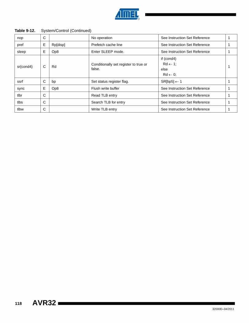
nop C No operation See Instruction Set Reference 1
pref E Rp[disp] Prefetch cache line See Instruction Set Reference 1
sleep E Op8 Enter SLEEP mode. See Instruction Set Reference 1
sr{cond4} C RdConditionally set register to true or false.
if (cond4)
Rd ← 1;else
Rd ← 0;
1
ssrf C bp Set status register flag. SR[bp5] ← 1 1
sync E Op8 Flush write buffer See Instruction Set Reference 1
tlbr C Read TLB entry See Instruction Set Reference 1
tlbs C Search TLB for entry See Instruction Set Reference 1
tlbw C Write TLB entry See Instruction Set Reference 1
Table 9-12. System/Control (Continued)
11832000D–04/2011
AVR32
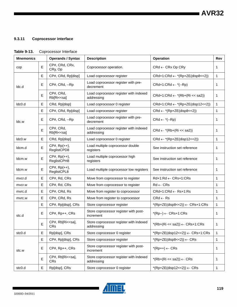
AVR32
9.3.11 Coprocessor interface
Table 9-13. Coprocessor Interface
Mnemonics Operands / Syntax Description Operation Rev
cop ECP#, CRd, CRx, CRy, Op
Coprocessor operation. CRd ← CRx Op CRy 1
ldc.d
E CP#, CRd, Rp[disp] Load coprocessor register CRd+1:CRd ← *(Rp+ZE(disp8<<2)) 1
E CP#, CRd, --RpLoad coprocessor register with pre-decrement
CRd+1:CRd ← *(--Rp) 1
ECP#, CRd, Rb[Ri<<sa]
Load coprocessor register with indexed addressing
CRd+1:CRd ← *(Rb+(Ri << sa2)) 1
ldc0.d E CRd, Rp[disp] Load coprocessor 0 register CRd+1:CRd ← *(Rp+ZE(disp12<<2)) 1
ldc.w
E CP#, CRd, Rp[disp] Load coprocessor register CRd ← *(Rp+ZE(disp8<<2)) 1
E CP#, CRd, --RpLoad coprocessor register with pre-decrement
CRd ← *(--Rp) 1
ECP#, CRd, Rb[Ri<<sa]
Load coprocessor register with indexed addressing
CRd ← *(Rb+(Ri << sa2)) 1
ldc0.w E CRd, Rp[disp] Load coprocessor 0 register CRd ← *(Rp+ZE(disp12<<2)) 1
ldcm.d ECP#, Rp{++}, ReglistCPD8
Load multiple coprocessor double registers
See instruction set reference 1
ldcm.w ECP#, Rp{++}, ReglistCPH8
Load multiple coprocessor high registers
See instruction set reference 1
ldcm.w ECP#, Rp{++}, ReglistCPL8
Load multiple coprocessor low registers See instruction set reference 1
mvcr.d E CP#, Rd, CRs Move from coprocessor to register Rd+1:Rd ← CRs+1:CRs 1
mvcr.w E CP#, Rd, CRs Move from coprocessor to register Rd ← CRs 1
mvrc.d E CP#, CRd, Rs Move from register to coprocessor CRd+1:CRd ← Rs+1:Rs 1
mvrc.w E CP#, CRd, Rs Move from register to coprocessor CRd ← Rs 1
stc.d
E CP#, Rp[disp], CRs Store coprocessor register *(Rp+ZE(disp8<<2)) ← CRs+1:CRs 1
E CP#, Rp++, CRsStore coprocessor register with post-increment
*(Rp--) ← CRs+1:CRs 1
ECP#, Rb[Ri<<sa], CRs
Store coprocessor register with indexed addressing
*(Rb+(Ri << sa2)) ← CRs+1:CRs 1
stc0.d E Rp[disp], CRs Store coprocessor 0 register *(Rp+ZE(disp12<<2)) ← CRs+1:CRs 1
stc.w
E CP#, Rp[disp], CRs Store coprocessor register *(Rp+ZE(disp8<<2)) ← CRs 1
E CP#, Rp++, CRsStore coprocessor register with post-increment
*(Rp++) ← CRs 1
ECP#, Rb[Ri<<sa], CRs
Store coprocessor register with indexed addressing
*(Rb+(Ri << sa2)) ← CRs 1
stc0.d E Rp[disp], CRs Store coprocessor 0 register *(Rp+ZE(disp12<<2)) ← CRs 1
11932000D–04/2011
9.3.12 Instructions to aid Java execution
9.3.13 SIMD Operations
stcm.d ECP#, {--}Rp, ReglistCPD8
Store multiple coprocessor double registers
See instruction set reference 1
stcm.w ECP#, {--}Rp, ReglistCPH8
Store multiple coprocessor high registers
See instruction set reference 1
stcm.w ECP#, {--}Rp, ReglistCPL8
Store multiple coprocessor low registers See instruction set reference 1
Table 9-13. Coprocessor Interface (Continued)
Table 9-14. Instructions to aid Java (Card) execution
Mnemonics Operands / Syntax Description Operation Rev
incjosp C imm Increment Java stack pointer JOSP + {-4, -3, -2, -1, 1, 2, 3, 4} 1
popjc C Pop Java context from Frame See instruction set reference 1
pushjc C Push Java context to Frame See instruction set reference 1
retj C Return from Java Trap See instruction set reference 1
Table 9-15. SIMD Operations
Mnemonics Operands / Syntax Description Operation Rev
pabs.{sb/sh} E Rd, Rs Packed Absolute Value See instruction set reference 1
packsh.{ub/sb} E Rd, Rx, Ry Pack Halfwords to Bytes See instruction set reference 1
packw.sh E Rd, Rx, Ry Pack Words to Halfwords See instruction set reference 1
padd.{b/h} E Rd, Rx, Ry Packed Addition See instruction set reference 1
paddh.{ub/sh} E Rd, Rx, Ry Packed Addition with halving See instruction set reference 1
padds.{ub/sb/uh/sh} E Rd, Rx, Ry Packed Addition with Saturation See instruction set reference 1
paddsub.h ERd, Rx:<part>, Ry:<part>
Packed Halfword Addition and Subtraction
See instruction set reference 1
paddsubh.sh ERd, Rx:<part>, Ry:<part>
Packed Halfword Addition and Subtraction with halving
See instruction set reference 1
paddsubs.{uh/sh} ERd, Rx:<part>, Ry:<part> Packed Halfword Addition and
Subtraction with SaturationSee instruction set reference 1
paddx.h E Rd, Rx, RyPacked Halfword Addition with Crossed Operand
See instruction set reference 1
paddxh.sh E Rd, Rx, RyPacked Halfword Addition with Crossed Operand and Halving
See instruction set reference 1
paddxs.{uh/sh} E Rd, Rx, RyPacked Halfword Addition with Crossed Operand and Saturation
See instruction set reference 1
pasr.{b/h} E Rd, Rs, {sa} Packed Arithmetic Shift Left See instruction set reference 1
pavg.{ub/sh} E Rd, Rx, Ry Packed Average See instruction set reference 1
plsl.{b/h} E Rd, Rs, {sa} Packed Logic Shift Left See instruction set reference 1
12032000D–04/2011
AVR32
AVR32
9.3.14 Memory read-modify-write instructions
plsr.{b/h} E Rd, Rs, {sa} Packed Logic Shift Right See instruction set reference 1
pmax.{ub/sh} E Rd, Rx, Ry Packed Maximum Value See instruction set reference 1
pmin.{ub/sh} E Rd, Rx, Ry Packed Minimum Value See instruction set reference 1
psad E Rd, Rx, Ry Sum of Absolute Differences See instruction set reference 1
psub.{b/h} E Rd, Rx, Ry Packed Subtraction See instruction set reference 1
psubadd.h ERd, Rx:<part>, Ry:<part> Packed Halfword Subtraction and
AdditionSee instruction set reference 1
psubaddh.sh ERd, Rx:<part>, Ry:<part>
Packed Halfword Subtraction and Addition with halving See instruction set reference 1
psubadds.{uh/sh} ERd, Rx:<part>, Ry:<part> Packed Halfword Subtraction and
Addition with SaturationSee instruction set reference 1
psubh.{ub/sh} E Rd, Rx, Ry Packed Subtraction with halving See instruction set reference 1
psubs.{ub/sb/uh/sh} E Rd, Rx, Ry Packed Subtraction with Saturation See instruction set reference 1
psubx.h E Rd, Rx, RyPacked Halfword Subtraction with Crossed Operand
See instruction set reference 1
psubxh.sh E Rd, Rx, RyPacked Halfword Subtraction with Crossed Operand and Halving
See instruction set reference 1
psubxs.{uh/sh} E Rd, Rx, RyPacked Halfword Subtraction with Crossed Operand and Saturation
See instruction set reference 1
punpck{ub/sb}.h E Rd, Rs:<part> Unpack Bytes to Halfwords See instruction set reference 1
Table 9-15. SIMD Operations (Continued)
Table 9-16. Memory read-modify-write Instructions
Mnemonics Operands / Syntax Description Operation Rev
memc E imm, bp Clear bit in memory Memory[(imm15<<2)[bp5]] = 0 1
mems E imm, bp Set bit in memory Memory[(imm15<<2)[bp5]] = 1 1
memt E imm, bp Toggle bit in memoryMemory[(imm15<<2)[bp5]] = ¬Memory[(imm15<<2)[bp5]]
1
12132000D–04/2011
9.4 Base Instruction Set DescriptionThe following chapter describes the instructions in the base instruction set.
12232000D–04/2011
AVR32
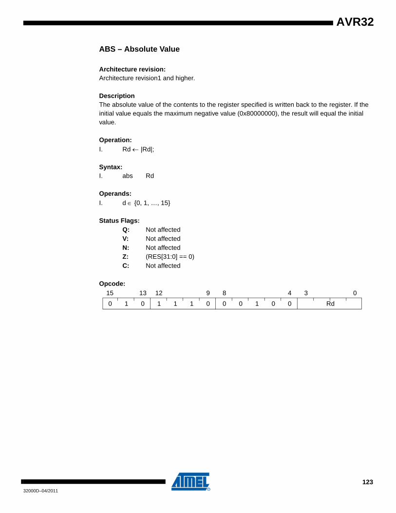
AVR32
ABS – Absolute Value
Architecture revision:Architecture revision1 and higher.
DescriptionThe absolute value of the contents to the register specified is written back to the register. If the initial value equals the maximum negative value (0x80000000), the result will equal the initial value.
Operation:I. Rd ← |Rd|;
Syntax:I. abs Rd
Operands:I. d ∈ {0, 1, …, 15}
Status Flags:Q: Not affectedV: Not affectedN: Not affectedZ: (RES[31:0] == 0)C: Not affected
Opcode:
0 1 0 1 1 1 0 0 0 1 0 0 Rd
15 13 12 9 8 4 3 0
12332000D–04/2011

ACALL – Application Call
Architecture revision:Architecture revision1 and higher.
DescriptionThe ACALL instruction performs an application function call.
Operation:I. LR ← PC + 2;
PC ← *(ACBA + (ZE(disp8)<<2));
Syntax:I. acall disp
Operands:I. disp ∈ {0, 4, ..., 1020}
Status Flags:Q: Not affectedV: Not affectedN: Not affectedZ: Not affectedC: Not affected
Opcode:
Note:ACBA must be word aligned. Failing to align ACBA correctly may lead to erronous be-havior.
1 1 0 1 disp8/Label 0 0 0 0
15 12 11 4 3 1 0
12432000D–04/2011
AVR32
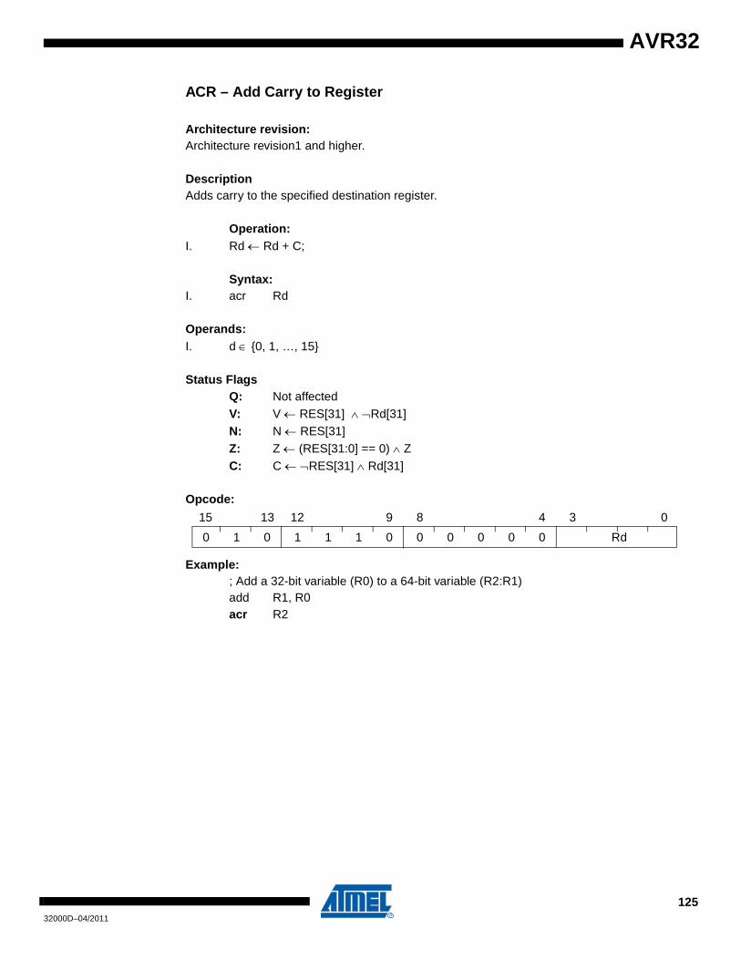
AVR32
ACR – Add Carry to Register
Architecture revision:Architecture revision1 and higher.
DescriptionAdds carry to the specified destination register.
Operation:I. Rd ← Rd + C;
Syntax:I. acr Rd
Operands:I. d ∈ {0, 1, …, 15}
Status FlagsQ: Not affectedV: V ← RES[31] ∧ ¬Rd[31]N: N ← RES[31]Z: Z ← (RES[31:0] == 0) ∧ ZC: C ← ¬RES[31] ∧ Rd[31]
Opcode:
Example:; Add a 32-bit variable (R0) to a 64-bit variable (R2:R1)add R1, R0acr R2
0 1 0 1 1 1 0 0 0 0 0 0 Rd
15 13 12 9 8 4 3 0
12532000D–04/2011
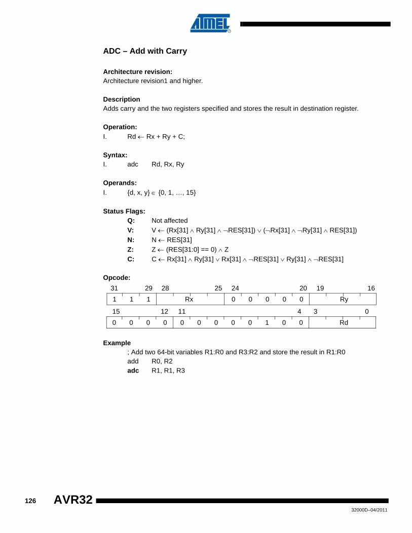
ADC – Add with Carry
Architecture revision:Architecture revision1 and higher.
DescriptionAdds carry and the two registers specified and stores the result in destination register.
Operation:I. Rd ← Rx + Ry + C;
Syntax:I. adc Rd, Rx, Ry
Operands:I. {d, x, y} ∈ {0, 1, …, 15}
Status Flags:Q: Not affectedV: V ← (Rx[31] ∧ Ry[31] ∧ ¬RES[31]) ∨ (¬Rx[31] ∧ ¬Ry[31] ∧ RES[31])N: N ← RES[31]Z: Z ← (RES[31:0] == 0) ∧ ZC: C ← Rx[31] ∧ Ry[31] ∨ Rx[31] ∧ ¬RES[31] ∨ Ry[31] ∧ ¬RES[31]
Opcode:
Example; Add two 64-bit variables R1:R0 and R3:R2 and store the result in R1:R0add R0, R2adc R1, R1, R3
1 1 1 Rx 0 0 0 0 0 Ry
31 29 28 25 24 20 19 16
0 0 0 0 0 0 0 0 0 1 0 0 Rd
15 12 11 4 3 0
12632000D–04/2011
AVR32
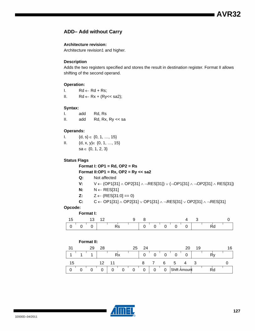
AVR32
ADD– Add without Carry
Architecture revision:Architecture revision1 and higher.
DescriptionAdds the two registers specified and stores the result in destination register. Format II allows shifting of the second operand.
Operation:I. Rd ← Rd + Rs;II. Rd ← Rx + (Ry<< sa2);
Syntax:I. add Rd, RsII. add Rd, Rx, Ry << sa
Operands:I. {d, s} ∈ {0, 1, …, 15}II. {d, x, y}∈ {0, 1, …, 15}
sa ∈ {0, 1, 2, 3}
Status FlagsFormat I: OP1 = Rd, OP2 = RsFormat II:OP1 = Rx, OP2 = Ry << sa2Q: Not affectedV: V ← (OP1[31] ∧ OP2[31] ∧ ¬RES[31]) ∨ (¬OP1[31] ∧ ¬OP2[31] ∧ RES[31])N: N ← RES[31] Z: Z ← (RES[31:0] == 0)C: C ← OP1[31] ∧ OP2[31] ∨ OP1[31] ∧ ¬RES[31] ∨ OP2[31] ∧ ¬RES[31]
Opcode:Format I:
Format II:
0 0 0 Rs 0 0 0 0 0 Rd
15 13 12 9 8 4 3 0
1 1 1 Rx 0 0 0 0 0 Ry
31 29 28 25 24 20 19 16
0 0 0 0 0 0 0 0 0 0 Shift Amount Rd
15 12 11 8 7 6 5 4 3 0
12732000D–04/2011

ADD{cond4} – Conditional Add
Architecture revision:Architecture revision 2 and higher.
DescriptionPerforms an addition and stores the result in destination register.
Operation:I. if ( cond4)
Rd ← Rx + Ry;
Syntax:I. add{cond4}Rd, Rx, Ry
Operands:I. {d, x, y} ∈ {0, 1, …, 15}
cond4 ∈ {eq, ne, cc/hs, cs/lo, ge, lt, mi, pl, ls, gt, le, hi, vs, vc, qs, al}
Status Flags:Q: Not affected.V: Not affected.N: Not affected.Z: Not affected.C: Not affected.
Opcode:
1 1 1 1 1 1 0 1 Ry
31 29 28 25 24 20 19 16
1 1 1 0 cond4 0 0 0 0 Rd
15 12 11 8 7 0
Rx
12832000D–04/2011
AVR32
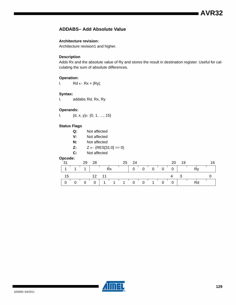
AVR32
ADDABS– Add Absolute Value
Architecture revision:Architecture revision1 and higher.
DescriptionAdds Rx and the absolute value of Ry and stores the result in destination register. Useful for cal-culating the sum of absolute differences.
Operation:I. Rd ← Rx + |Ry|;
Syntax:I. addabs Rd, Rx, Ry
Operands:I. {d, x, y}∈ {0, 1, …, 15}
Status FlagsQ: Not affectedV: Not affectedN: Not affected Z: Z ← (RES[31:0] == 0)C: Not affected
Opcode:
1 1 1 Rx 0 0 0 0 0 Ry
31 29 28 25 24 20 19 16
0 0 0 0 1 1 1 0 0 1 0 0 Rd
15 12 11 4 3 0
12932000D–04/2011
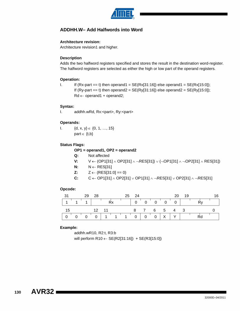
ADDHH.W– Add Halfwords into Word
Architecture revision:Architecture revision1 and higher.
DescriptionAdds the two halfword registers specified and stores the result in the destination word-register. The halfword registers are selected as either the high or low part of the operand registers.
Operation:I. If (Rx-part == t) then operand1 = SE(Rx[31:16]) else operand1 = SE(Rx[15:0]);
If (Ry-part == t) then operand2 = SE(Ry[31:16]) else operand2 = SE(Ry[15:0]);Rd ← operand1 + operand2;
Syntax:I. addhh.wRd, Rx:<part>, Ry:<part>
Operands:I. {d, x, y} ∈ {0, 1, …, 15}
part ∈ {t,b}
Status Flags:OP1 = operand1, OP2 = operand2Q: Not affectedV: V ← (OP1[31] ∧ OP2[31] ∧ ¬RES[31]) ∨ (¬OP1[31] ∧ ¬OP2[31] ∧ RES[31])N: N ← RES[31] Z: Z ← (RES[31:0] == 0)C: C ← OP1[31] ∧ OP2[31] ∨ OP1[31] ∧ ¬RES[31] ∨ OP2[31] ∧ ¬RES[31]
Opcode:
Example:addhh.wR10, R2:t, R3:bwill perform R10 ← SE(R2[31:16]) + SE(R3[15:0])
1 1 1 Rx 0 0 0 0 0 Ry
31 29 28 25 24 20 19 16
0 0 0 0 1 1 1 0 0 0 X Y Rd
15 12 11 8 7 6 5 4 3 0
13032000D–04/2011
AVR32

AVR32
AND – Logical AND with optional logical shift
Architecture revision:Architecture revision1 and higher.
DescriptionPerforms a bitwise logical AND between the specified registers and stores the result in the desti-nation register.
Operation:I. Rd ← Rd ∧ Rs;II. Rd ← Rx ∧ (Ry << sa5);III. Rd ← Rx ∧ (Ry >> sa5);
Syntax:I. and Rd, RsII. and Rd, Rx, Ry << saIII. and Rd, Rx, Ry >> sa
Operands:I. {d, s} ∈ {0, 1, …, 15}II, III {d, x, y} ∈ {0, 1, …, 15}
sa ∈ {0, 1, …, 31}
Status FlagsQ: Not affectedV: Not affectedN: N ← RES[31]Z: Z ← (RES[31:0] == 0)C: Not affected
OpcodeFormat I:
Format II:
0 0 0 Rs 0 0 1 1 0 Rd
15 13 12 9 8 4 3 0
1 1 1 Rx 1 1 1 1 0 Ry
31 29 28 25 24 20 19 16
0 0 0 0 0 0 0 sa5 Rd
15 9 8 4 3 0
13132000D–04/2011

Format III:
1 1 1 Rx 1 1 1 1 0 Ry
31 29 28 25 24 20 19 16
0 0 0 0 0 0 1 sa5 Rd
15 9 8 4 3 0
13232000D–04/2011
AVR32

AVR32
AND{cond4} – Conditional And
Architecture revision:Architecture revision1 and higher.
Architecture revision:Architecture revision 2 and higher.
DescriptionPerforms a bitwise logical AND between the specified registers and stores the result in the desti-nation register.
Operation:I. if ( cond4)
Rd ← Rx ∧ Ry;
Syntax:I. and{cond4}Rd, Rx, Ry
Operands:I. {d, x, y} ∈ {0, 1, …, 15}
cond4 ∈ {eq, ne, cc/hs, cs/lo, ge, lt, mi, pl, ls, gt, le, hi, vs, vc, qs, al}
Status Flags:Q: Not affected.V: Not affected.N: Not affected.Z: Not affected.C: Not affected.
Opcode:
1 1 1 1 1 1 0 1 Ry
31 29 28 25 24 20 19 16
1 1 1 0 cond4 0 0 1 0 Rd
15 12 11 8 7 0
Rx
13332000D–04/2011
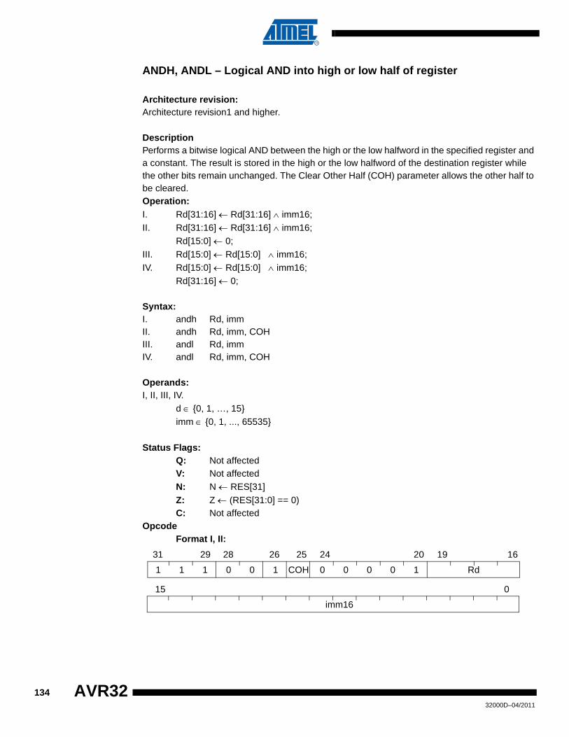
ANDH, ANDL – Logical AND into high or low half of register
Architecture revision:Architecture revision1 and higher.
DescriptionPerforms a bitwise logical AND between the high or the low halfword in the specified register and a constant. The result is stored in the high or the low halfword of the destination register while the other bits remain unchanged. The Clear Other Half (COH) parameter allows the other half to be cleared.Operation:I. Rd[31:16] ← Rd[31:16] ∧ imm16;II. Rd[31:16] ← Rd[31:16] ∧ imm16;
Rd[15:0] ← 0;III. Rd[15:0] ← Rd[15:0] ∧ imm16;IV. Rd[15:0] ← Rd[15:0] ∧ imm16;
Rd[31:16] ← 0;
Syntax:I. andh Rd, immII. andh Rd, imm, COHIII. andl Rd, immIV. andl Rd, imm, COH
Operands:I, II, III, IV.
d ∈ {0, 1, …, 15}imm ∈ {0, 1, ..., 65535}
Status Flags:Q: Not affectedV: Not affectedN: N ← RES[31]Z: Z ← (RES[31:0] == 0)C: Not affected
OpcodeFormat I, II:
1 1 1 0 0 1 COH 0 0 0 0 1 Rd
31 29 28 26 25 24 20 19 16
imm16
15 0
13432000D–04/2011
AVR32
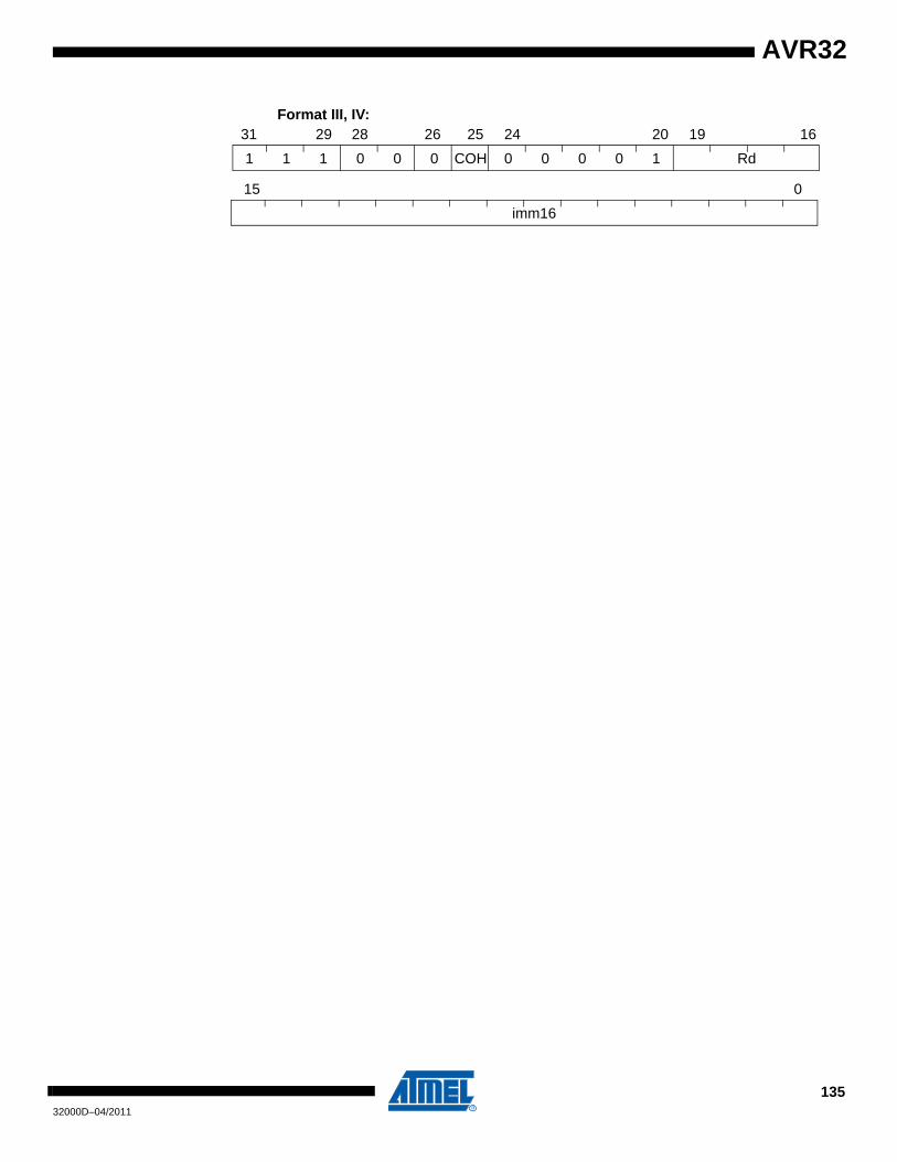
AVR32
Format III, IV:
1 1 1 0 0 0 COH 0 0 0 0 1 Rd
31 29 28 26 25 24 20 19 16
imm16
15 0
13532000D–04/2011
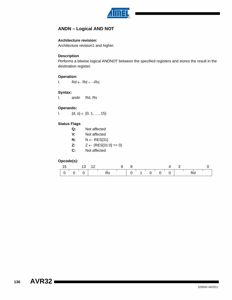
ANDN – Logical AND NOT
Architecture revision:Architecture revision1 and higher.
DescriptionPerforms a bitwise logical ANDNOT between the specified registers and stores the result in the destination register.
Operation:I. Rd ← Rd ∧ ¬Rs;
Syntax:I. andn Rd, Rs
Operands:I. {d, s} ∈ {0, 1, …, 15}
Status FlagsQ: Not affectedV: Not affectedN: N ← RES[31]Z: Z ← (RES[31:0] == 0)C: Not affected
Opcode(s):
0 0 0 Rs 0 1 0 0 0 Rd
15 13 12 9 8 4 3 0
13632000D–04/2011
AVR32
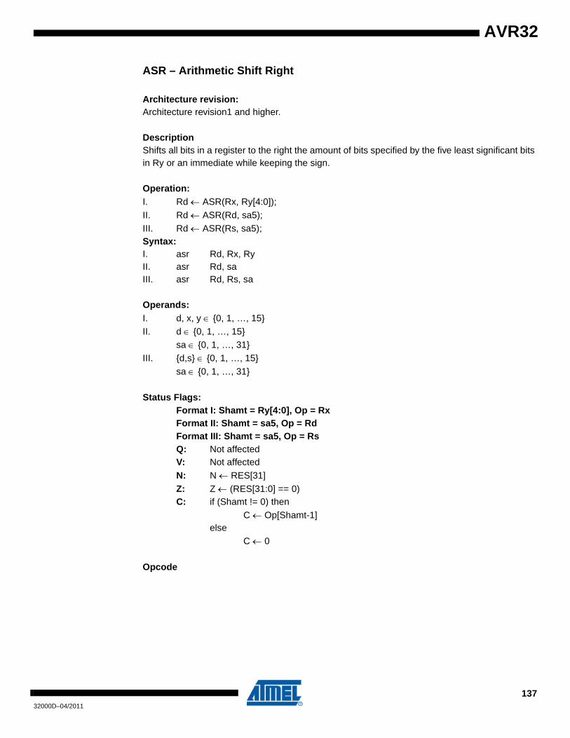
AVR32
ASR – Arithmetic Shift Right
Architecture revision:Architecture revision1 and higher.
DescriptionShifts all bits in a register to the right the amount of bits specified by the five least significant bits in Ry or an immediate while keeping the sign.
Operation:I. Rd ← ASR(Rx, Ry[4:0]);II. Rd ← ASR(Rd, sa5); III. Rd ← ASR(Rs, sa5);Syntax:I. asr Rd, Rx, RyII. asr Rd, saIII. asr Rd, Rs, sa
Operands:I. d, x, y ∈ {0, 1, …, 15}II. d ∈ {0, 1, …, 15}
sa ∈ {0, 1, …, 31}III. {d,s} ∈ {0, 1, …, 15}
sa ∈ {0, 1, …, 31}
Status Flags:Format I: Shamt = Ry[4:0], Op = RxFormat II: Shamt = sa5, Op = RdFormat III: Shamt = sa5, Op = RsQ: Not affectedV: Not affectedN: N ← RES[31]Z: Z ← (RES[31:0] == 0)C: if (Shamt != 0) then
C ← Op[Shamt-1]else
C ← 0
Opcode
13732000D–04/2011
Format I:
Format II:
Format III:
1 1 1 Rx 0 0 0 0 0 Ry
31 29 28 25 24 20 19 16
0 0 0 0 1 0 0 0 0 1 0 0 Rd
15 12 11 4 3 0
1 0 1 Bit[4:1] 1 0 1 0 Bit[0] Rd
15 13 12 9 8 5 4 3 0
1 1 1 Rs 0 0 0 0 0 Rd
31 29 28 25 24 20 19 16
0 0 0 1 0 1 0 0 0 0 0 sa5
15 12 11 8 7 5 4 0
13832000D–04/2011
AVR32
AVR32
BFEXTS – Bitfield extract and sign-extend
Architecture revision:Architecture revision1 and higher.
DescriptionThis instruction extracts and sign-extends the w5 bits in Rs starting at bit-offset bp5 to Rd.
Operation:I. Rd ← SE(Rs[bp5+w5-1:bp5]);
Syntax:I. bfexts Rd, Rs, bp5, w5
Operands:I. {d, s} ∈ {0, 1, …, 15}
{bp5, w5} ∈ {0, 1, ..., 31}
Status Flags:Q: Not affectedV: Not affectedN: N ← RES[31]Z: Z ← (RES[31:0] == 0)C: C ← RES[31]
Opcode:Format I:
Note:If (w5 = 0) or if (bp5 + w5 > 32) the result is undefined.
1 1 1 Rd 1 1 1 0 1 Rs
31 29 28 25 24 20 19 16
1 0 1 1 0 0 bp5 w5
15 12 11 10 9 5 4 0
13932000D–04/2011
BFEXTU – Bitfield extract and zero-extend
Architecture revision:Architecture revision1 and higher.
DescriptionThis instruction extracts and zero-extends the w5 bits in Rs starting at bit-offset bp5 to Rd.
Operation:I. Rd ← ZE(Rs[bp5+w5-1:bp5]);
Syntax:I. bfextu Rd, Rs, bp5, w5
Operands:I. {d, s} ∈ {0, 1, …, 15}
{bp5, w5} ∈ {0, 1, ..., 31}
Status Flags:Q: Not affectedV: Not affectedN: N ← RES[31]Z: Z ← (RES[31:0] == 0)C: C ← RES[31]
Opcode:
Format I:
Note:If (w5 = 0) or if (bp5 + w5 > 32) the result is undefined.
1 1 1 Rd 1 1 1 0 1 Rs
31 29 28 25 24 20 19 16
1 1 0 0 0 0 bp5 w5
15 12 11 10 9 5 4 0
14032000D–04/2011
AVR32
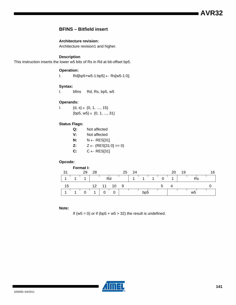
AVR32
BFINS – Bitfield insert
Architecture revision:Architecture revision1 and higher.
DescriptionThis instruction inserts the lower w5 bits of Rs in Rd at bit-offset bp5.
Operation:I. Rd[bp5+w5-1:bp5] ← Rs[w5-1:0];
Syntax:I. bfins Rd, Rs, bp5, w5
Operands:I. {d, s} ∈ {0, 1, …, 15}
{bp5, w5} ∈ {0, 1, ..., 31}
Status Flags:Q: Not affectedV: Not affectedN: N ← RES[31]Z: Z ← (RES[31:0] == 0)C: C ← RES[31]
Opcode:
Format I:
Note:If (w5 = 0) or if (bp5 + w5 > 32) the result is undefined.
1 1 1 Rd 1 1 1 0 1 Rs
31 29 28 25 24 20 19 16
1 1 0 1 0 0 bp5 w5
15 12 11 10 9 5 4 0
14132000D–04/2011
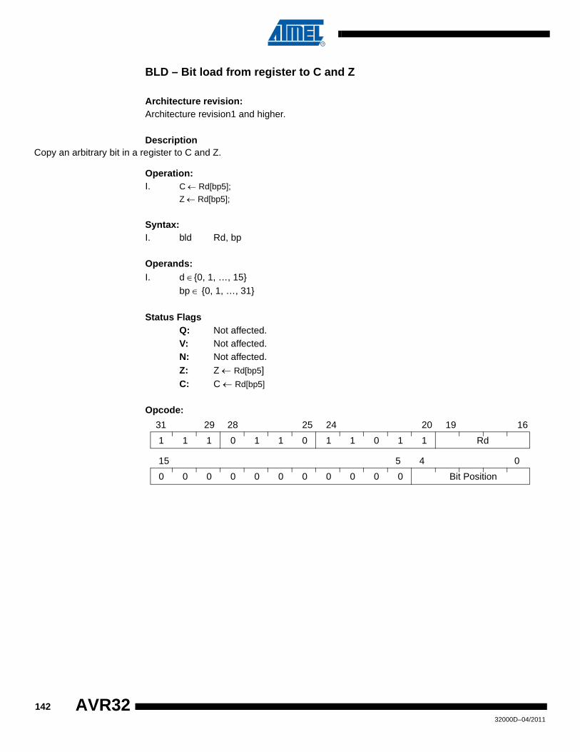
BLD – Bit load from register to C and Z
Architecture revision:Architecture revision1 and higher.
DescriptionCopy an arbitrary bit in a register to C and Z.
Operation:I. C ← Rd[bp5];
Z ← Rd[bp5];
Syntax:I. bld Rd, bp
Operands: I. d ∈{0, 1, …, 15}
bp ∈ {0, 1, …, 31}
Status FlagsQ: Not affected.V: Not affected.N: Not affected.Z: Z ← Rd[bp5]C: C ← Rd[bp5]
Opcode:
1 1 1 0 1 1 0 1 1 0 1 1 Rd
31 29 28 25 24 20 19 16
0 0 0 0 0 0 0 0 0 0 0 Bit Position
15 5 4 0
14232000D–04/2011
AVR32

AVR32
BR{cond} – Branch if Condition Satisfied
Architecture revision:Architecture revision1 and higher.
DescriptionBranch if the specified condition is satisfied.
Operation:I. if (cond3)
PC ← PC + (SE(disp8) << 1);else
PC ← PC + 2;
II. if (cond4)PC ← PC + (SE(disp21) << 1);
elsePC ← PC + 4;
Syntax:I. br{cond3}dispII. br{cond4}disp
Operands:I. cond3 ∈ {eq, ne, cc/hs, cs/lo, ge, lt, mi, pl}
disp ∈ {-256, -254, ..., 254}II. cond4 ∈ {eq, ne, cc/hs, cs/lo, ge, lt, mi, pl, ls, gt, le, hi, vs, vc, qs, al}
disp ∈ {-2097152, -2097150, ..., 2097150}
Status Flags:Q: Not affected.V: Not affected.N: Not affected.Z: Not affected.C: Not affected.
Opcode:Format I:
1 1 0 0 disp8 0 cond3
15 13 12 11 4 3 2 0
14332000D–04/2011

Format II:
1 1 1 disp21[20:1 0 1 0 0 d21 cond4
31 29 28 25 24 20 19 16
disp21[15:0]
15 0
[16]
14432000D–04/2011
AVR32
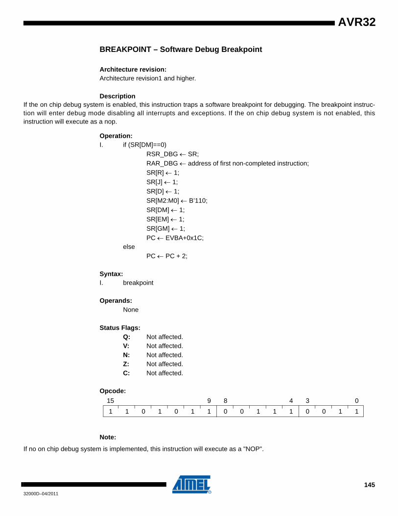
AVR32
BREAKPOINT – Software Debug Breakpoint
Architecture revision:Architecture revision1 and higher.
DescriptionIf the on chip debug system is enabled, this instruction traps a software breakpoint for debugging. The breakpoint instruc-tion will enter debug mode disabling all interrupts and exceptions. If the on chip debug system is not enabled, thisinstruction will execute as a nop.
Operation:I. if (SR[DM]==0)
RSR_DBG ← SR;RAR_DBG ← address of first non-completed instruction;SR[R] ← 1;SR[J] ← 1;SR[D] ← 1;SR[M2:M0] ← B’110;SR[DM] ← 1;SR[EM] ← 1;SR[GM] ← 1;PC ← EVBA+0x1C;
elsePC ← PC + 2;
Syntax:I. breakpoint
Operands:None
Status Flags:Q: Not affected.V: Not affected.N: Not affected.Z: Not affected.C: Not affected.
Opcode:
Note:
If no on chip debug system is implemented, this instruction will execute as a "NOP".
1 1 0 1 0 1 1 0 0 1 1 1 0 0 1 1
15 9 8 4 3 0
14532000D–04/2011
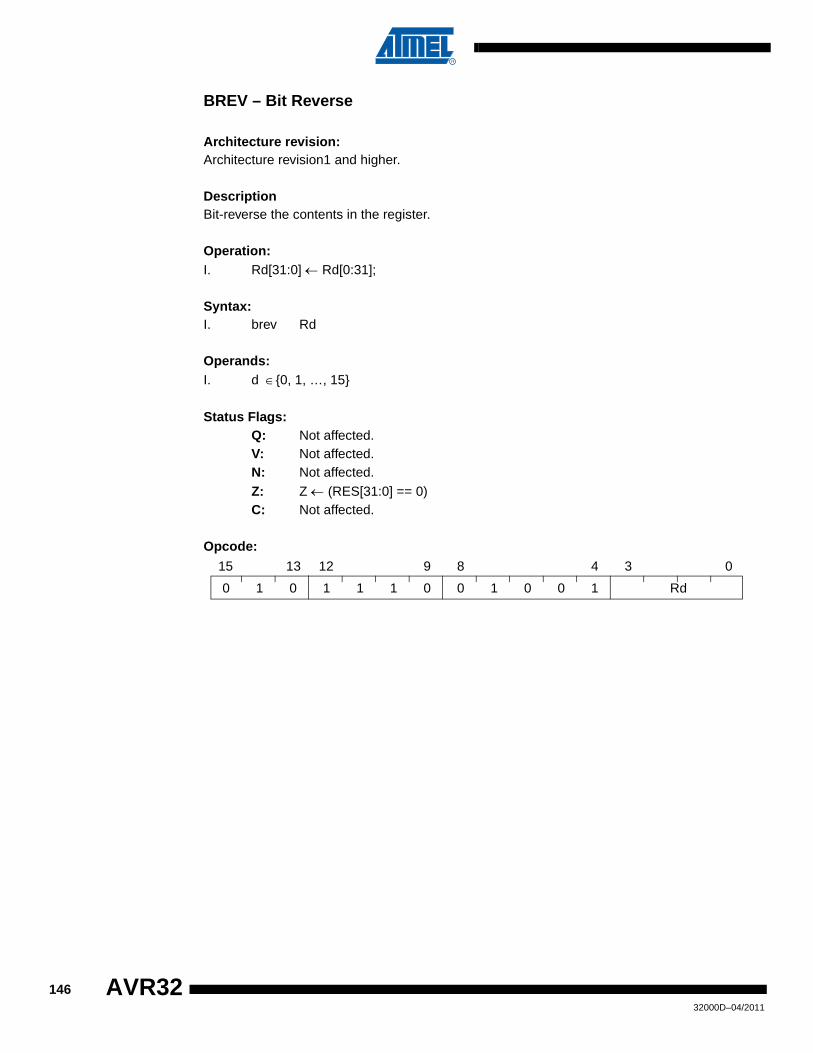
BREV – Bit Reverse
Architecture revision:Architecture revision1 and higher.
DescriptionBit-reverse the contents in the register.
Operation:I. Rd[31:0] ← Rd[0:31];
Syntax:I. brev Rd
Operands: I. d ∈{0, 1, …, 15}
Status Flags:Q: Not affected.V: Not affected.N: Not affected.Z: Z ← (RES[31:0] == 0)C: Not affected.
Opcode:
0 1 0 1 1 1 0 0 1 0 0 1 Rd
15 13 12 9 8 4 3 0
14632000D–04/2011
AVR32
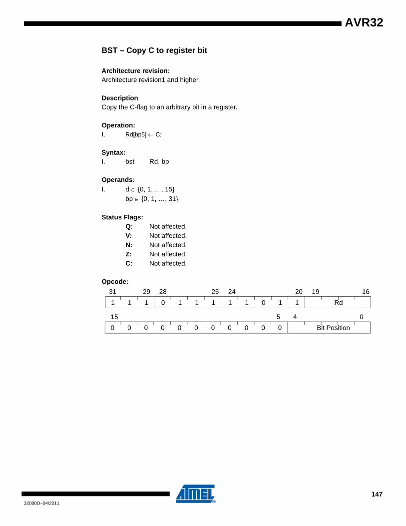
AVR32
BST – Copy C to register bit
Architecture revision:Architecture revision1 and higher.
DescriptionCopy the C-flag to an arbitrary bit in a register.
Operation:I. Rd[bp5] ← C;
Syntax:I. bst Rd, bp
Operands:I. d ∈ {0, 1, …, 15}
bp ∈ {0, 1, …, 31}
Status Flags:Q: Not affected.V: Not affected.N: Not affected.Z: Not affected.C: Not affected.
Opcode:
1 1 1 0 1 1 1 1 0 1 1 Rd
31 29 28 25 24 20 19 16
0 0 0 0 0 0 0 0 0 0 0 Bit Position
15 5 4 0
1
14732000D–04/2011
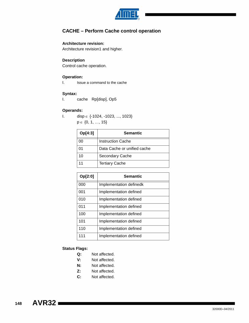
CACHE – Perform Cache control operation
Architecture revision:Architecture revision1 and higher.
DescriptionControl cache operation.
Operation:I. Issue a command to the cache
Syntax:I. cache Rp[disp], Op5
Operands:I. disp ∈ {-1024, -1023, ..., 1023}
p ∈ {0, 1, …, 15}
Status Flags:Q: Not affected.V: Not affected.N: Not affected.Z: Not affected.C: Not affected.
Op[4:3] Semantic
00 Instruction Cache
01 Data Cache or unified cache
10 Secondary Cache
11 Tertiary Cache
Op[2:0] Semantic
000 Implementation definedk
001 Implementation defined
010 Implementation defined
011 Implementation defined
100 Implementation defined
101 Implementation defined
110 Implementation defined
111 Implementation defined
14832000D–04/2011
AVR32
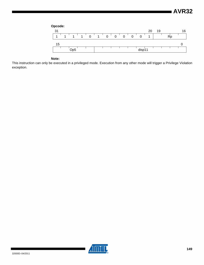
AVR32
Opcode:
Note: This instruction can only be executed in a privileged mode. Execution from any other mode will trigger a Privilege Violationexception.
1 1 1 1 1 0 0 0 0 0 1 Rp
31 20 19 16
Op5 disp11
15 0
0
14932000D–04/2011
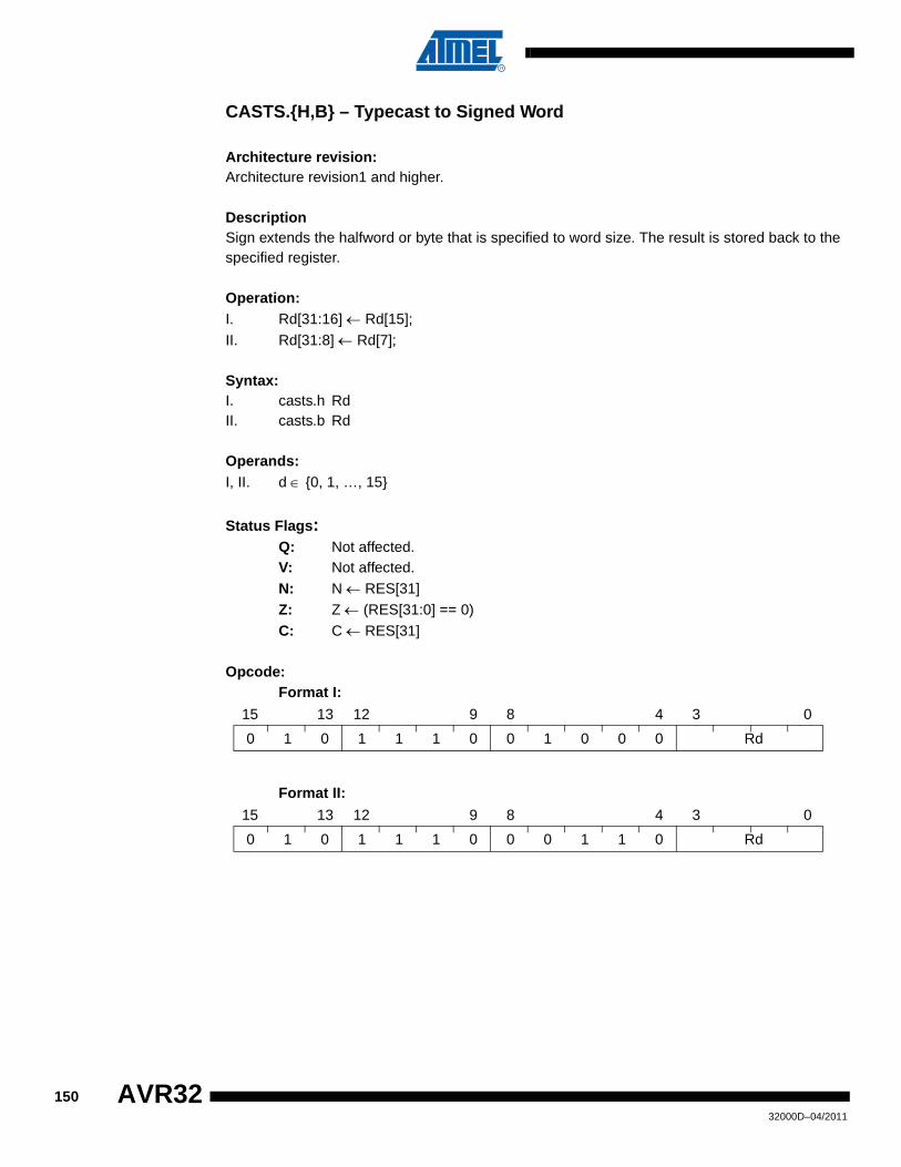
CASTS.{H,B} – Typecast to Signed Word
Architecture revision:Architecture revision1 and higher.
DescriptionSign extends the halfword or byte that is specified to word size. The result is stored back to the specified register.
Operation:I. Rd[31:16] ← Rd[15];II. Rd[31:8] ← Rd[7];
Syntax:I. casts.h RdII. casts.b Rd
Operands:I, II. d ∈ {0, 1, …, 15}
Status Flags:Q: Not affected.V: Not affected.N: N ← RES[31]Z: Z ← (RES[31:0] == 0)C: C ← RES[31]
Opcode:Format I:
Format II:
0 1 0 1 1 1 0 0 1 0 0 0 Rd
15 13 12 9 8 4 3 0
0 1 0 1 1 1 0 0 0 1 1 0 Rd
15 13 12 9 8 4 3 0
15032000D–04/2011
AVR32

AVR32
CASTU.{H,B} – Typecast to Unsigned Word
Architecture revision:Architecture revision1 and higher.
DescriptionZero extends the halfword or byte that is specified to word size. The result is stored back to the specified register.
Operation:I. Rd[31:16] ← 0;II. Rd[31:8] ← 0:
Syntax:I. castu.h RdII. castu.b Rd
Operands:I, II. d ∈ {0, 1, …, 15}
Status Flags:Q: Not affected.V: Not affected.N: N ← RES[31]Z: Z ← (RES[31:0] == 0)C: C ← RES[31]
Opcode:Format I:
Format II:
0 1 0 1 1 1 0 0 0 1 1 1 Rd
15 13 12 9 8 4 3 0
0 1 0 1 1 1 0 0 0 1 0 1 Rd
15 13 12 9 8 4 3 0
15132000D–04/2011

CBR – Clear Bit in Register
Architecture revision:Architecture revision1 and higher.
DescriptionClears a bit in the specified register. All other bits are unaffected.
Operation:I. Rd[bp5] ← 0;
Syntax:I. cbr Rd, bp
Operands:I. d ∈ {0, 1, …, 15}
bp ∈ {0, 1, …, 31}
Status Flags:Q: Not affectedV: Not affectedN: Not affectedZ: Z ← (RES[31:0] == 0)C: Not affected
Opcode:
1 0 1 Bit[4:1] 1 1 1 0 Bit[0] Rd
15 13 12 9 8 5 4 3 0
15232000D–04/2011
AVR32
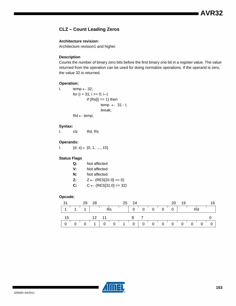
AVR32
CLZ – Count Leading Zeros
Architecture revision:Architecture revision1 and higher.
DescriptionCounts the number of binary zero bits before the first binary one bit in a register value. The value returned from the operation can be used for doing normalize operations. If the operand is zero, the value 32 is returned.
Operation:I. temp ← 32;
for (i = 31; i >= 0; i--)if (Rs[i] == 1) then
temp ← 31 - i;break;
Rd ← temp;
Syntax:I. clz Rd, Rs
Operands:I. {d, s} ∈ {0, 1, …, 15}
Status FlagsQ: Not affectedV: Not affectedN: Not affectedZ: Z ← (RES[31:0] == 0)C: C ← (RES[31:0] == 32)
Opcode:
1 1 1 Rs 0 0 0 0 0 Rd
31 29 28 25 24 20 19 16
0 0 0 1 0 0 1 0 0 0 0 0 0 0 0 0
15 12 11 8 7 0
15332000D–04/2011
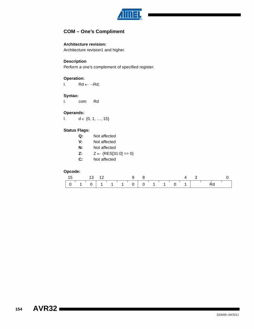
COM – One’s Compliment
Architecture revision:Architecture revision1 and higher.
DescriptionPerform a one’s complement of specified register.
Operation:I. Rd ← ¬Rd;
Syntax:I. com Rd
Operands:I. d ∈ {0, 1, …, 15}
Status Flags:Q: Not affectedV: Not affectedN: Not affectedZ: Z ← (RES[31:0] == 0)C: Not affected
Opcode:
0 1 0 1 1 1 0 0 1 1 0 1 Rd
15 13 12 9 8 4 3 0
15432000D–04/2011
AVR32
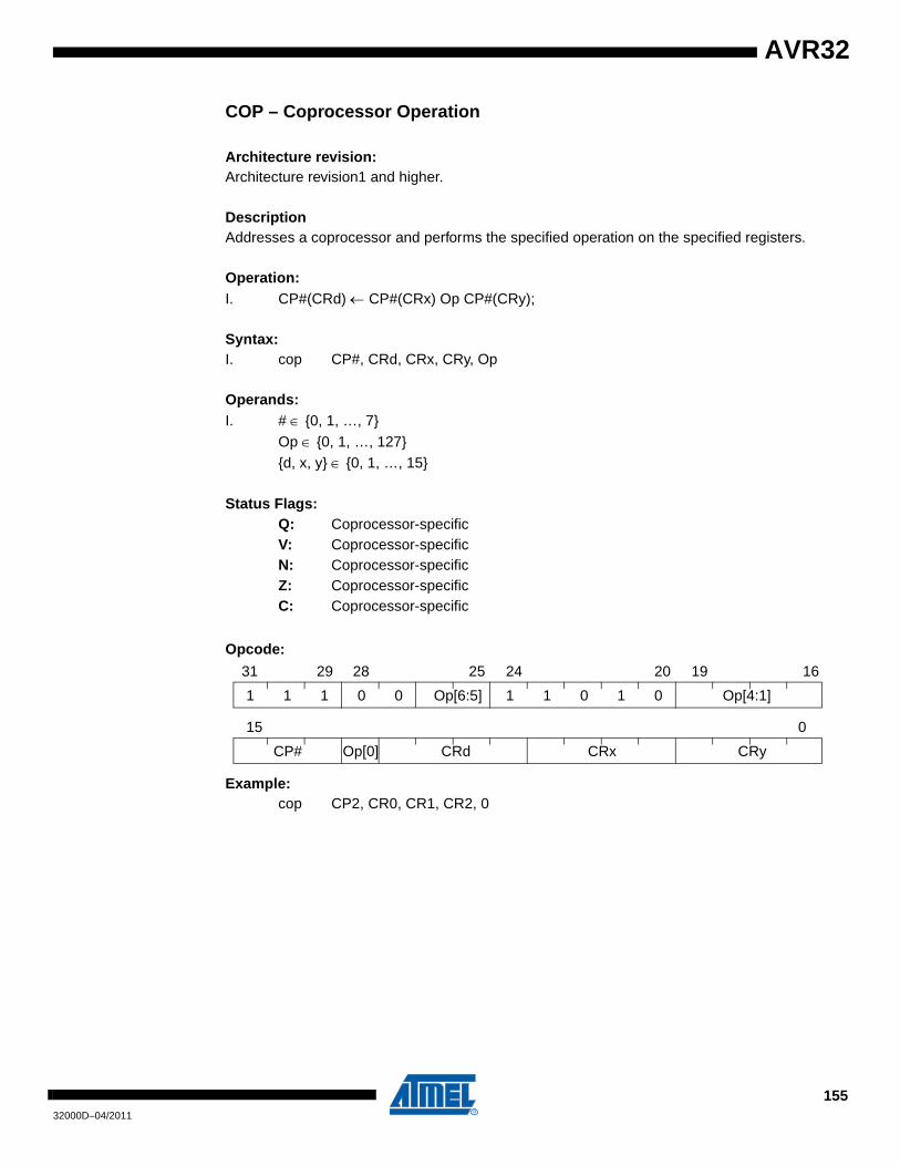
AVR32
COP – Coprocessor Operation
Architecture revision:Architecture revision1 and higher.
DescriptionAddresses a coprocessor and performs the specified operation on the specified registers.
Operation:I. CP#(CRd) ← CP#(CRx) Op CP#(CRy);
Syntax:I. cop CP#, CRd, CRx, CRy, Op
Operands:I. # ∈ {0, 1, …, 7}
Op ∈ {0, 1, …, 127}{d, x, y} ∈ {0, 1, …, 15}
Status Flags:Q: Coprocessor-specificV: Coprocessor-specificN: Coprocessor-specificZ: Coprocessor-specificC: Coprocessor-specific
Opcode:
Example:cop CP2, CR0, CR1, CR2, 0
1 1 1 0 0 Op[6:5] 1 1 0 1 0 Op[4:1]
31 29 28 25 24 20 19 16
CP# Op[0] CRd CRx CRy
15 0
15532000D–04/2011
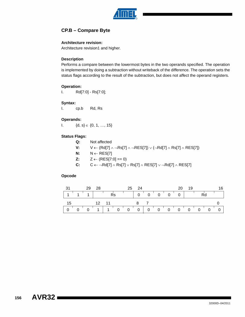
CP.B – Compare Byte
Architecture revision:Architecture revision1 and higher.
DescriptionPerforms a compare between the lowermost bytes in the two operands specified. The operation is implemented by doing a subtraction without writeback of the difference. The operation sets the status flags according to the result of the subtraction, but does not affect the operand registers.
Operation:I. Rd[7:0] - Rs[7:0];
Syntax:I. cp.b Rd, Rs
Operands:I. {d, s} ∈ {0, 1, …, 15}
Status Flags:Q: Not affectedV: V ← (Rd[7] ∧ ¬Rs[7] ∧ ¬RES[7]) ∨ (¬Rd[7] ∧ Rs[7] ∧ RES[7])N: N ← RES[7]Z: Z ← (RES[7:0] == 0)C: C ← ¬Rd[7] ∧ Rs[7] ∨ Rs[7] ∧ RES[7] ∨ ¬Rd[7] ∧ RES[7]
Opcode
1 1 1 Rs 0 0 0 0 0 Rd
31 29 28 25 24 20 19 16
0 0 0 1 1 0 0 0 0 0 0 0 0 0 0 0
15 12 11 8 7 0
15632000D–04/2011
AVR32
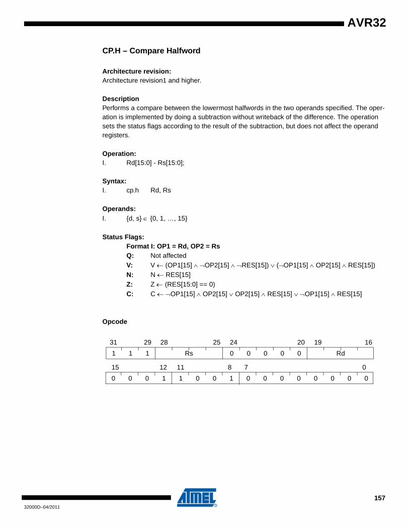
AVR32
CP.H – Compare Halfword
Architecture revision:Architecture revision1 and higher.
DescriptionPerforms a compare between the lowermost halfwords in the two operands specified. The oper-ation is implemented by doing a subtraction without writeback of the difference. The operation sets the status flags according to the result of the subtraction, but does not affect the operand registers.
Operation:I. Rd[15:0] - Rs[15:0];
Syntax:I. cp.h Rd, Rs
Operands:I. {d, s} ∈ {0, 1, …, 15}
Status Flags:Format I: OP1 = Rd, OP2 = RsQ: Not affectedV: V ← (OP1[15] ∧ ¬OP2[15] ∧ ¬RES[15]) ∨ (¬OP1[15] ∧ OP2[15] ∧ RES[15])N: N ← RES[15]Z: Z ← (RES[15:0] == 0)C: C ← ¬OP1[15] ∧ OP2[15] ∨ OP2[15] ∧ RES[15] ∨ ¬OP1[15] ∧ RES[15]
Opcode
1 1 1 Rs 0 0 0 0 0 Rd
31 29 28 25 24 20 19 16
0 0 0 1 1 0 0 1 0 0 0 0 0 0 0 0
15 12 11 8 7 0
15732000D–04/2011
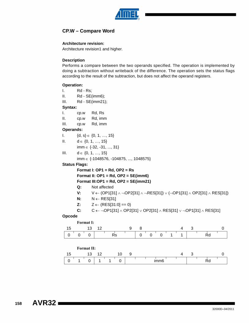
CP.W – Compare Word
Architecture revision:Architecture revision1 and higher.
DescriptionPerforms a compare between the two operands specified. The operation is implemented bydoing a subtraction without writeback of the difference. The operation sets the status flagsaccording to the result of the subtraction, but does not affect the operand registers.
Operation:I. Rd - Rs;II. Rd - SE(imm6);III. Rd - SE(imm21);Syntax:I. cp.w Rd, RsII. cp.w Rd, immIII. cp.w Rd, immOperands:I. {d, s} ∈ {0, 1, …, 15}II. d ∈ {0, 1, …, 15}
imm ∈ {-32, -31, ..., 31}III. d ∈ {0, 1, …, 15}
imm ∈ {-1048576, -104875, ..., 1048575}Status Flags:
Format I: OP1 = Rd, OP2 = RsFormat II: OP1 = Rd, OP2 = SE(imm6)Format III:OP1 = Rd, OP2 = SE(imm21)Q: Not affectedV: V ← (OP1[31] ∧ ¬OP2[31] ∧ ¬RES[31]) ∨ (¬OP1[31] ∧ OP2[31] ∧ RES[31])N: N ← RES[31]Z: Z ← (RES[31:0] == 0)C: C ← ¬OP1[31] ∧ OP2[31] ∨ OP2[31] ∧ RES[31] ∨ ¬OP1[31] ∧ RES[31]
Opcode
Format I:
Format II:
0 0 0 Rs 0 0 0 1 1 Rd
15 13 12 9 8 4 3 0
0 1 0 1 1 0 imm6 Rd
15 13 12 10 9 4 3 0
15832000D–04/2011
AVR32
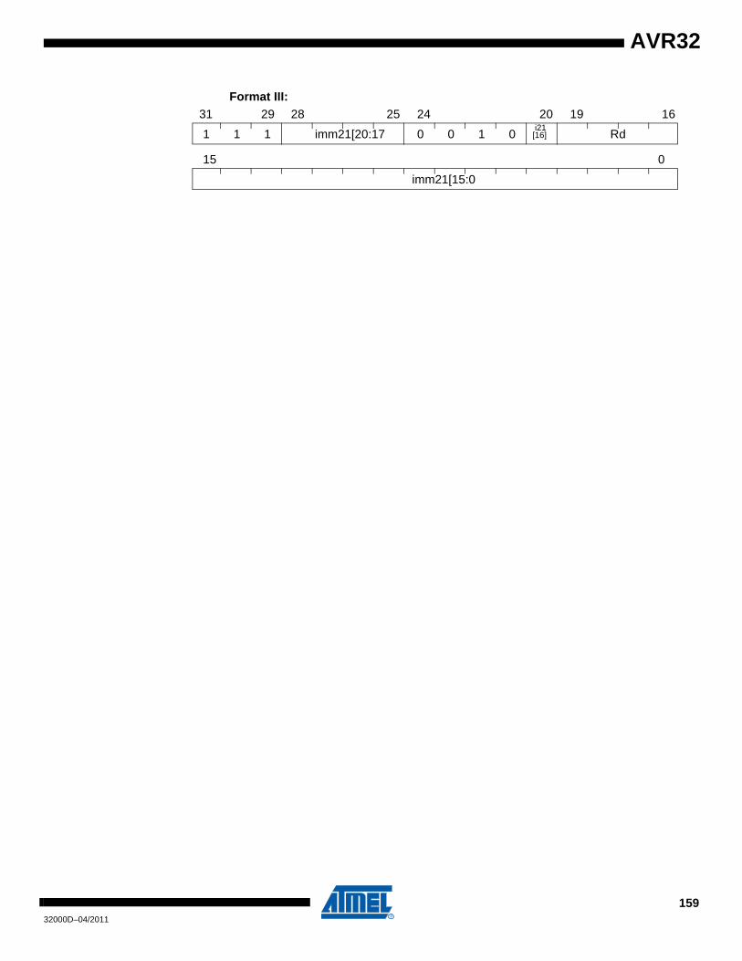
AVR32
Format III:
1 1 1 imm21[20:17 0 0 1 0i21
Rd
31 29 28 25 24 20 19 16
imm21[15:0
15 0
[16]
15932000D–04/2011
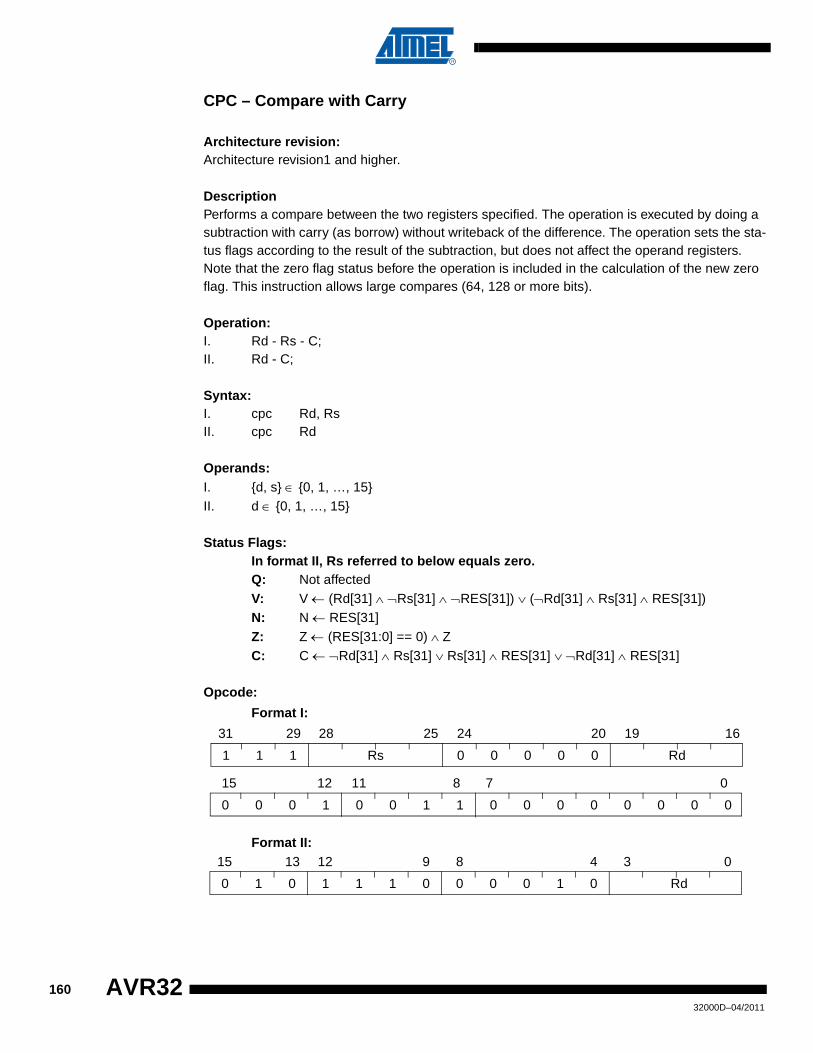
CPC – Compare with Carry
Architecture revision:Architecture revision1 and higher.
DescriptionPerforms a compare between the two registers specified. The operation is executed by doing a subtraction with carry (as borrow) without writeback of the difference. The operation sets the sta-tus flags according to the result of the subtraction, but does not affect the operand registers. Note that the zero flag status before the operation is included in the calculation of the new zero flag. This instruction allows large compares (64, 128 or more bits).
Operation:I. Rd - Rs - C;II. Rd - C;
Syntax:I. cpc Rd, RsII. cpc Rd
Operands:I. {d, s} ∈ {0, 1, …, 15}II. d ∈ {0, 1, …, 15}
Status Flags:In format II, Rs referred to below equals zero.Q: Not affectedV: V ← (Rd[31] ∧ ¬Rs[31] ∧ ¬RES[31]) ∨ (¬Rd[31] ∧ Rs[31] ∧ RES[31])N: N ← RES[31]Z: Z ← (RES[31:0] == 0) ∧ ZC: C ← ¬Rd[31] ∧ Rs[31] ∨ Rs[31] ∧ RES[31] ∨ ¬Rd[31] ∧ RES[31]
Opcode:
Format I:
Format II:
1 1 1 Rs 0 0 0 0 0 Rd
31 29 28 25 24 20 19 16
0 0 0 1 0 0 1 1 0 0 0 0 0 0 0 0
15 12 11 8 7 0
0 1 0 1 1 1 0 0 0 0 1 0 Rd
15 13 12 9 8 4 3 0
16032000D–04/2011
AVR32

AVR32
CSRF – Clear Status Register Flag
Architecture revision:Architecture revision1 and higher.
DescriptionClears the status register (SR) flag specified.
Operation:I. SR[bp5] ← 0;
Syntax:I. csrf bp
Operands:I. bp ∈ {0, 1, …, 31}
Status Flags:SR[bp5] ← 0, all other flags unchanged.
Opcode:
Note:Privileged if bp5 > 15, ie. upper half of status register. An exception will be triggered if the upper half of the status register is attempted changed in user mode.
1 1 0 1 0 1 0 bp5 0 0 1 1
15 11 10 9 8 4 3 0
16132000D–04/2011

CSRFCZ – Copy Status Register Flag to C and Z
Architecture revision:Architecture revision1 and higher.
DescriptionCopies the status register (SR) flag specified to C and Z.
Operation:I. C ← SR[bp5];
Z ← SR[bp5];
Syntax:I. csrfcz bp
Operands:I. bp ∈ {0, 1, …, 31}
Status Flags:Q: Not affectedV: Not affectedN: Not affectedZ: Z ← SR[bp5]C: C ← SR[bp5]
Opcode:
Note:Privileged if bp5 > 15, ie. upper half of status register. A Privilege Violation exception will be trig-gered if the upper half of the status register is attempted read in user mode.
1 1 0 1 0 0 0 bp5 0 0 1 1
15 11 10 9 8 4 3 0
16232000D–04/2011
AVR32
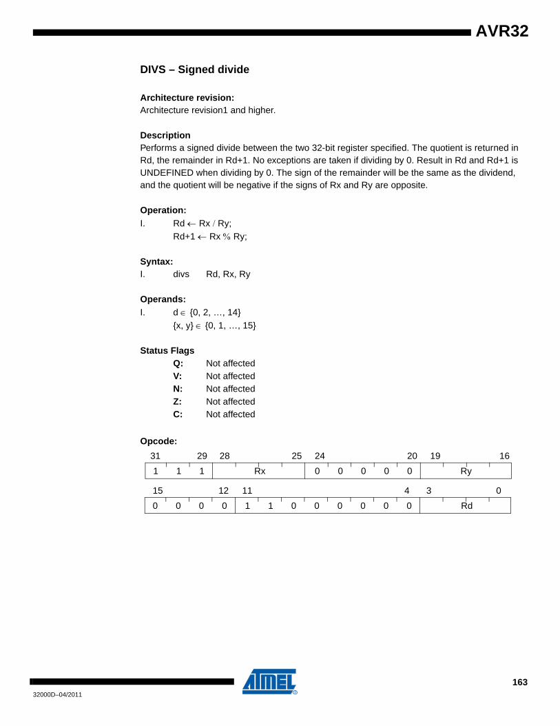
AVR32
DIVS – Signed divide
Architecture revision:Architecture revision1 and higher.
DescriptionPerforms a signed divide between the two 32-bit register specified. The quotient is returned in Rd, the remainder in Rd+1. No exceptions are taken if dividing by 0. Result in Rd and Rd+1 is UNDEFINED when dividing by 0. The sign of the remainder will be the same as the dividend, and the quotient will be negative if the signs of Rx and Ry are opposite.
Operation:I. Rd ← Rx / Ry;
Rd+1 ← Rx % Ry;
Syntax:I. divs Rd, Rx, Ry
Operands:I. d ∈ {0, 2, …, 14}
{x, y} ∈ {0, 1, …, 15}
Status FlagsQ: Not affectedV: Not affectedN: Not affectedZ: Not affectedC: Not affected
Opcode:
1 1 1 Rx 0 0 0 0 0 Ry
31 29 28 25 24 20 19 16
0 0 0 0 1 1 0 0 0 0 0 0 Rd
15 12 11 4 3 0
16332000D–04/2011
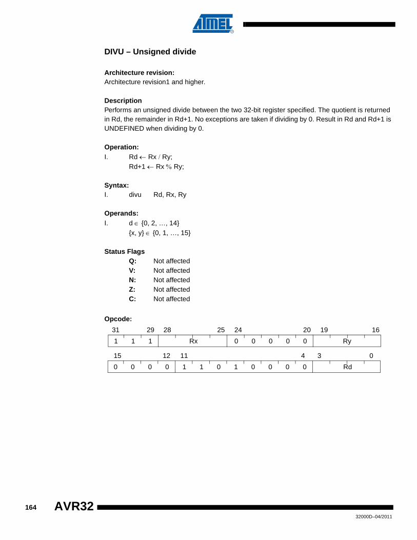
DIVU – Unsigned divide
Architecture revision:Architecture revision1 and higher.
DescriptionPerforms an unsigned divide between the two 32-bit register specified. The quotient is returned in Rd, the remainder in Rd+1. No exceptions are taken if dividing by 0. Result in Rd and Rd+1 is UNDEFINED when dividing by 0.
Operation:I. Rd ← Rx / Ry;
Rd+1 ← Rx % Ry;
Syntax:I. divu Rd, Rx, Ry
Operands:I. d ∈ {0, 2, …, 14}
{x, y} ∈ {0, 1, …, 15}
Status FlagsQ: Not affectedV: Not affectedN: Not affectedZ: Not affectedC: Not affected
Opcode:
1 1 1 Rx 0 0 0 0 0 Ry
31 29 28 25 24 20 19 16
0 0 0 0 1 1 0 1 0 0 0 0 Rd
15 12 11 4 3 0
16432000D–04/2011
AVR32

AVR32
EOR – Logical Exclusive OR with optional logical shift
Architecture revision:Architecture revision1 and higher.
DescriptionPerforms a bitwise logical Exclusive-OR between the specified registers and stores the result in the destination register.
Operation:I. Rd ← Rd ⊕ Rs;II. Rd ← Rx ⊕ (Ry << sa5);III. Rd ← Rx ⊕ (Ry >> sa5);
Syntax:I. eor Rd, RsII. eor Rd, Rx, Ry << saIII. eor Rd, Rx, Ry >> sa
Operands:I. {d, s} ∈ {0, 1, …, 15}II, III. {d, x, y} ∈ {0, 1, …, 15}
sa ∈ {0, 1, …, 31}
Status FlagsQ: Not affectedV: Not affectedN: N ← RES[31]Z: Z ← (RES[31:0] == 0)C: Not affected
Opcode:
Format I:
Format II:
0 0 0 Rs 0 0 1 0 1 Rd
15 13 12 9 8 4 3 0
1 1 1 Rx 1 1 1 1 0 Ry
31 29 28 25 24 20 19 16
0 0 1 0 0 0 0 sa5 Rd
15 9 8 4 3 0
16532000D–04/2011

Format III:
1 1 1 Rx 1 1 1 1 0 Ry
31 29 28 25 24 20 19 16
0 0 1 0 0 0 1 sa5 Rd
15 9 8 4 3 0
16632000D–04/2011
AVR32
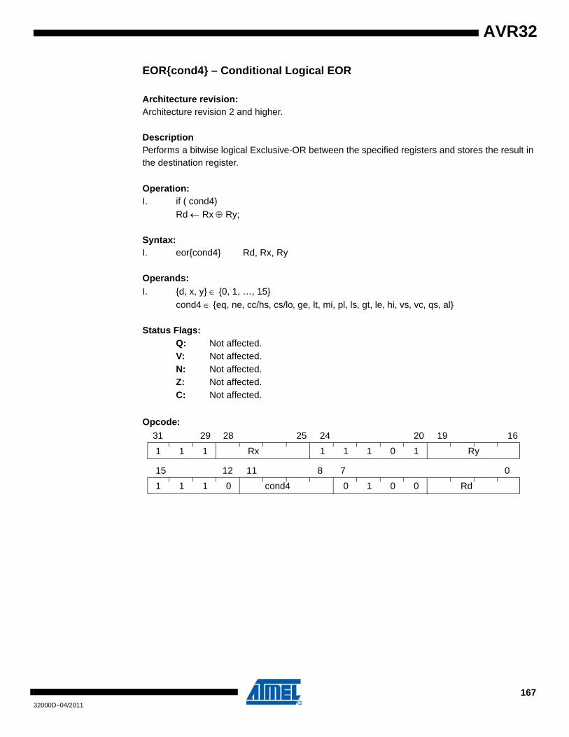
AVR32
EOR{cond4} – Conditional Logical EOR
Architecture revision:Architecture revision 2 and higher.
DescriptionPerforms a bitwise logical Exclusive-OR between the specified registers and stores the result in the destination register.
Operation:I. if ( cond4)
Rd ← Rx ⊕ Ry;
Syntax:I. eor{cond4} Rd, Rx, Ry
Operands:I. {d, x, y} ∈ {0, 1, …, 15}
cond4 ∈ {eq, ne, cc/hs, cs/lo, ge, lt, mi, pl, ls, gt, le, hi, vs, vc, qs, al}
Status Flags:Q: Not affected.V: Not affected.N: Not affected.Z: Not affected.C: Not affected.
Opcode:
1 1 1 1 1 1 0 1 Ry
31 29 28 25 24 20 19 16
1 1 1 0 cond4 0 1 0 0 Rd
15 12 11 8 7 0
Rx
16732000D–04/2011

EORH, EORL – Logical EOR into high or low half of register
Architecture revision:Architecture revision1 and higher.
DescriptionPerforms a bitwise logical Exclusive-OR between the high or low halfword in the specified regis-ter and a constant. The result is stored in the destination register.
Operation:I. Rd[31:16] ← Rd[31:16] ⊕ imm16II. Rd[15:0] ← Rd[15:0] ⊕ imm16
Syntax:I. eorh Rd, immII. eorl Rd, imm
Operands:I, II. d ∈ {0, 1, …, 15}
imm ∈ {0, 1, ..., 65535}
Status Flags:Q: Not affectedV: Not affectedN: N ← RES[31]Z: Z ← (RES[31:0] == 0)C: Not affected
Opcode
Format I:
Format II:
1 1 1 0 1 1 0 0 0 0 1 Rd
31 29 28 20 19 16
imm16
15 0
1
1 1 1 0 1 0 0 0 0 0 1 Rd
31 29 28 20 19 16
imm16
15 0
1
16832000D–04/2011
AVR32

AVR32
FRS – Flush Return Stack
Architecture revision:Architecture revision1 and higher.
DescriptionSpecial instruction to invalidate the return address stack. This instruction is used when the user writes code that conflicts with the semantics required by the return address stack.
Operation:I. Invalidate all entries in the return address stack.
Syntax:I. frs
Operands:I. none
Status Flags:Q: Not affectedV: Not affectedN: Not affected Z: Not affectedC: Not affected
Opcode:
Note:On implementation without a return stack this instruction will execute as a "NOP".
1 1 0 1 0 1 1 1 0 1 0 0 0 0 1 1
15 9 8 4 3 0
16932000D–04/2011
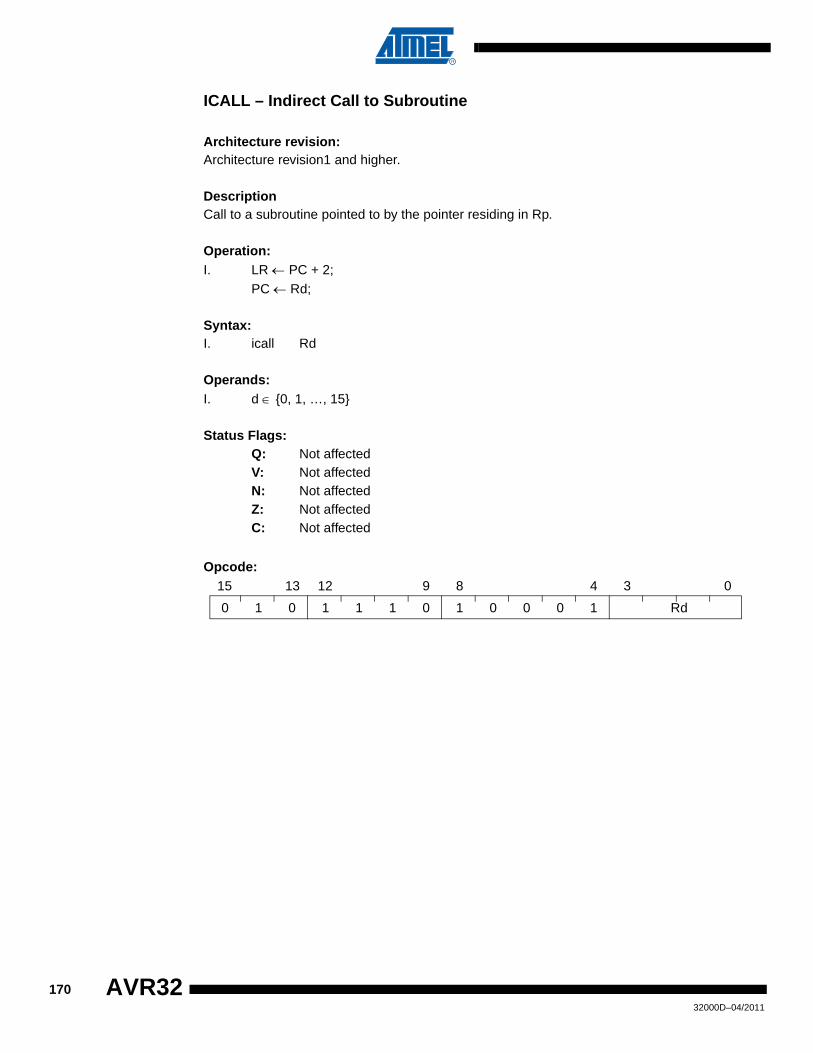
ICALL – Indirect Call to Subroutine
Architecture revision:Architecture revision1 and higher.
DescriptionCall to a subroutine pointed to by the pointer residing in Rp.
Operation:I. LR ← PC + 2;
PC ← Rd; Syntax:I. icall Rd
Operands:I. d ∈ {0, 1, …, 15}
Status Flags:Q: Not affectedV: Not affectedN: Not affectedZ: Not affectedC: Not affected
Opcode:
0 1 0 1 1 1 0 1 0 0 0 1 Rd
15 13 12 9 8 4 3 0
17032000D–04/2011
AVR32

AVR32
INCJOSP – Increment Java Operand Stack Pointer
Architecture revision:Architecture revision1 and higher.
DescriptionIncrement the system register "Java Operand Stack Pointer" with value.
Operation:I. if ( JOSP[3:0] + imm < 0 )
TRAP 4else if (JOSP[3:0] + imm > 8 )
TRAP 3else
JOSP ← JOSP + imm;
Syntax:I. incjosp imm
Operands:I. imm ∈ {-4, -3, -2, -1, 1, 2, 3, 4}
Status Flags:Q: Not affectedV: Not affectedN: Not affectedZ: Not affectedC: Not affected
Opcode:
imm3 imm
100 -4
101 -3
110 -2
111 -1
000 1
001 2
010 3
011 4
1 1 0 1 0 1 1 0 1 imm3 0 0 1 1
15 13 12 7 6 4 3 0
17132000D–04/2011

Note: When trapped, this instruction will destroy R12. It is the programmer’s responsibility to keep the R12value if needed.
17232000D–04/2011
AVR32
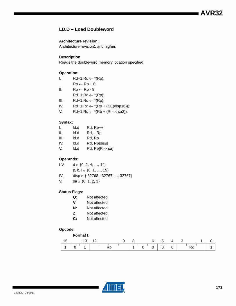
AVR32
LD.D – Load Doubleword
Architecture revision:Architecture revision1 and higher.
DescriptionReads the doubleword memory location specified.
Operation:I. Rd+1:Rd ← *(Rp);
Rp ← Rp + 8;II. Rp ← Rp - 8;
Rd+1:Rd ← *(Rp);III. Rd+1:Rd ← *(Rp);IV. Rd+1:Rd ← *(Rp + (SE(disp16)));V. Rd+1:Rd ← *(Rb + (Ri << sa2));
Syntax:I. ld.d Rd, Rp++II. ld.d Rd, --RpIII. ld.d Rd, RpIV. ld.d Rd, Rp[disp]V. ld.d Rd, Rb[Ri<<sa]
Operands:I-V. d ∈ {0, 2, 4, …, 14}
p, b, i ∈ {0, 1, …, 15}IV. disp ∈ {-32768, -32767, ..., 32767}V. sa ∈ {0, 1, 2, 3}
Status Flags:Q: Not affected.V: Not affected.N: Not affected.Z: Not affected.C: Not affected.
Opcode:
Format I:
1 0 1 Rp 1 0 0 0 0 Rd 1
15 13 12 9 8 6 5 4 3 1 0
17332000D–04/2011
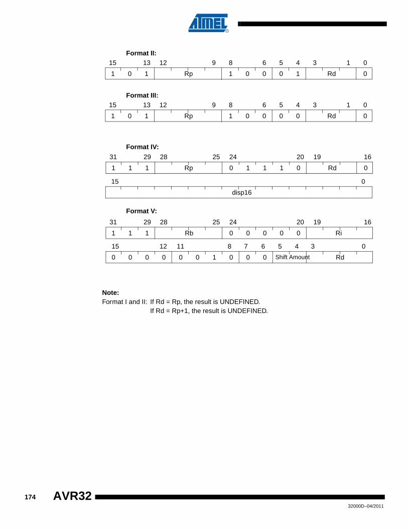
Format II:
Format III:
Format IV:
Format V:
Note:Format I and II: If Rd = Rp, the result is UNDEFINED.
If Rd = Rp+1, the result is UNDEFINED.
1 0 1 Rp 1 0 0 0 1 Rd 0
15 13 12 9 8 6 5 4 3 1 0
1 0 1 Rp 1 0 0 0 0 Rd 0
15 13 12 9 8 6 5 4 3 1 0
1 1 1 Rp 0 1 1 1 0 Rd 0
31 29 28 25 24 20 19 16
disp16
15 0
1 1 1 Rb 0 0 0 0 0 Ri
31 29 28 25 24 20 19 16
0 0 0 0 0 0 1 0 0 0 Shift Amount Rd
15 12 11 8 7 6 5 4 3 0
17432000D–04/2011
AVR32
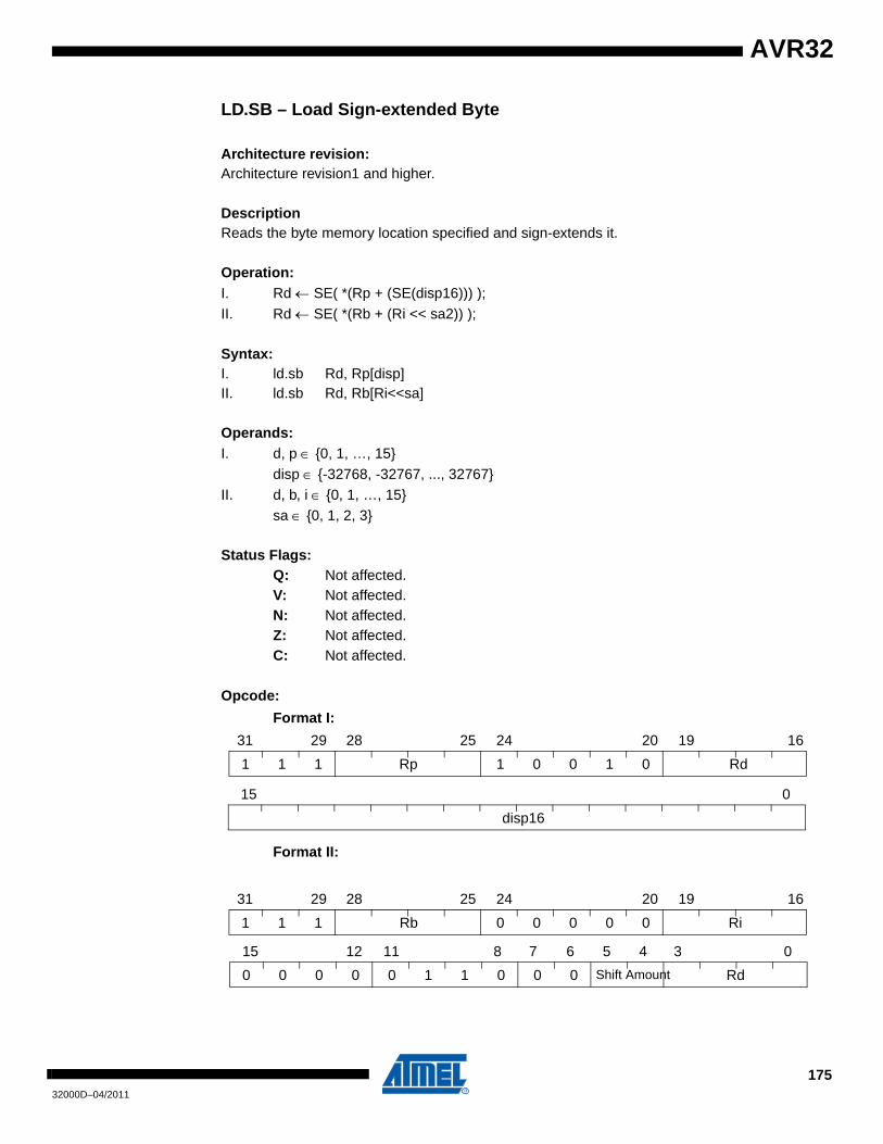
AVR32
LD.SB – Load Sign-extended Byte
Architecture revision:Architecture revision1 and higher.
DescriptionReads the byte memory location specified and sign-extends it.
Operation:I. Rd ← SE( *(Rp + (SE(disp16))) );II. Rd ← SE( *(Rb + (Ri << sa2)) );
Syntax:I. ld.sb Rd, Rp[disp]II. ld.sb Rd, Rb[Ri<<sa]
Operands:I. d, p ∈ {0, 1, …, 15}
disp ∈ {-32768, -32767, ..., 32767}II. d, b, i ∈ {0, 1, …, 15}
sa ∈ {0, 1, 2, 3}
Status Flags:Q: Not affected.V: Not affected.N: Not affected.Z: Not affected.C: Not affected.
Opcode:
Format I:
Format II:
1 1 1 Rp 1 0 0 1 0 Rd
31 29 28 25 24 20 19 16
disp16
15 0
1 1 1 Rb 0 0 0 0 0 Ri
31 29 28 25 24 20 19 16
0 0 0 0 0 1 1 0 0 0 Shift Amount Rd
15 12 11 8 7 6 5 4 3 0
17532000D–04/2011

LD.SB{cond4} – Conditionally Load Sign-extended Byte
Architecture revision: Architecture revision 2 and higher.
DescriptionReads the byte memory location specified and sign-extends it if the given condition is satisfied.
Operation:I. if (cond4)
Rd ← SE( *(Rp + (ZE(disp9))) );
Syntax:I. ld.sb{cond4} Rd, Rp[disp]
Operands:I. d, p ∈ {0, 1, …, 15}
disp ∈ {0, 1, ..., 511}cond4 ∈ {eq, ne, cc/hs, cs/lo, ge, lt, mi, pl, ls, gt, le, hi, vs, vc, qs, al}
Status Flags:Q: Not affected.V: Not affected.N: Not affected.Z: Not affected.C: Not affected.
Opcode:
1 1 1 1 1 1 1 1
31 29 28 25 24 20 19 16
cond4 0 1 1 disp9
15 12 11 8 7 6 5 4 3 0
RdRp
17632000D–04/2011
AVR32

AVR32
LD.UB – Load Zero-extended Byte
Architecture revision:Architecture revision1 and higher.
DescriptionReads the byte memory location specified and zero-extends it.
Operation:I. Rd ← ZE( *(Rp) );
Rp ← Rp + 1;II. Rp ← Rp - 1;
Rd ← ZE( *(Rp) );III. Rd ← ZE( *(Rp + (ZE(disp3))) );IV. Rd ← ZE( *(Rp + (SE(disp16))) );V. Rd ← ZE( *(Rb + (Ri << sa2)) );
Syntax:I. ld.ub Rd, Rp++II. ld.ub Rd, --RpIII. ld.ub Rd, Rp[disp]IV. ld.ub Rd, Rp[disp]V. ld.ub Rd, Rb[Ri<<sa]
Operands:I-V. d, p, b, i ∈ {0, 1, …, 15}III. disp ∈ {0, 1, ..., 7}IV. disp ∈ {-32768, -32767, ..., 32767}V. sa ∈ {0, 1, 2, 3}
Status Flags:Q: Not affected.V: Not affected.N: Not affected.Z: Not affected.C: Not affected.
Opcode:
Format I:
0 0 0 Rp 1 0 0 1 1 Rd
15 13 12 9 8 4 3 0
17732000D–04/2011

Format II:
Format III:
Format IV:
Format V:
Note:Format I and II: If Rd = Rp, the result is UNDEFINED.
0 0 0 Rp 1 0 1 1 1 Rd
15 13 12 9 8 4 3 0
0 0 0 Rp 1 1 disp3 Rd
15 13 12 9 8 7 6 4 3 0
1 1 1 Rp 1 0 0 1 1 Rd
31 29 28 25 24 20 19 16
disp16
15 0
1 1 1 Rb 0 0 0 0 0 Ri
31 29 28 25 24 20 19 16
0 0 0 0 0 1 1 1 0 0 Shift Amount Rd
15 12 11 8 7 6 5 4 3 0
17832000D–04/2011
AVR32

AVR32
LD.UB{cond4} – Conditionally Load Zero-extended Byte
Architecture revision: Architecture revision 2 and higher.
DescriptionReads the byte memory location specified and zero-extends it if the given condition is satisfied.
Operation:I. if (cond4)
Rd ← ZE( *(Rp + (ZE(disp9))) );
Syntax:I. ld.ub{cond4} Rd, Rp[disp]
Operands:I. d, p ∈ {0, 1, …, 15}
disp ∈ {0, 1, ..., 511}cond4 ∈ {eq, ne, cc/hs, cs/lo, ge, lt, mi, pl, ls, gt, le, hi, vs, vc, qs, al}
Status Flags:Q: Not affected.V: Not affected.N: Not affected.Z: Not affected.C: Not affected.
Opcode:
1 1 1 1 1 1 1 1
31 29 28 25 24 20 19 16
cond4 1 0 0 disp9
15 12 11 8 7 6 5 4 3 0
RdRp
17932000D–04/2011
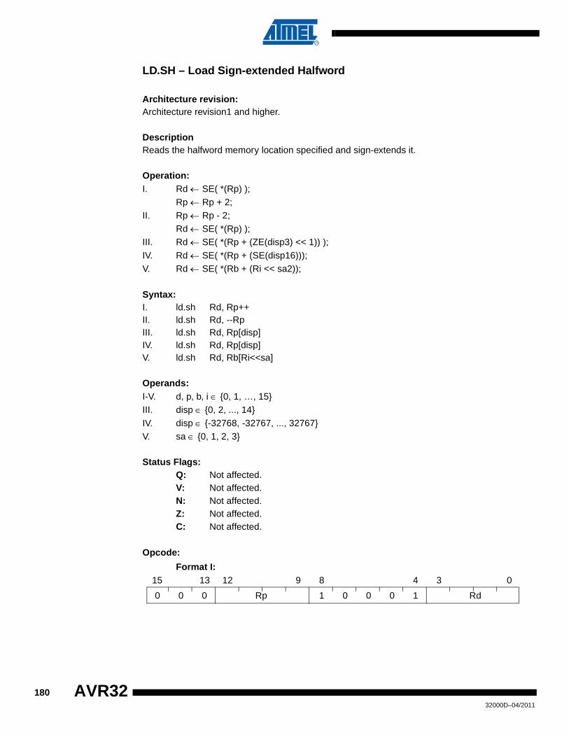
LD.SH – Load Sign-extended Halfword
Architecture revision:Architecture revision1 and higher.
DescriptionReads the halfword memory location specified and sign-extends it.
Operation:I. Rd ← SE( *(Rp) );
Rp ← Rp + 2;II. Rp ← Rp - 2;
Rd ← SE( *(Rp) );III. Rd ← SE( *(Rp + (ZE(disp3) << 1)) );IV. Rd ← SE( *(Rp + (SE(disp16)));V. Rd ← SE( *(Rb + (Ri << sa2));
Syntax:I. ld.sh Rd, Rp++II. ld.sh Rd, --RpIII. ld.sh Rd, Rp[disp]IV. ld.sh Rd, Rp[disp]V. ld.sh Rd, Rb[Ri<<sa]
Operands:I-V. d, p, b, i ∈ {0, 1, …, 15}III. disp ∈ {0, 2, ..., 14}IV. disp ∈ {-32768, -32767, ..., 32767}V. sa ∈ {0, 1, 2, 3}
Status Flags:Q: Not affected.V: Not affected.N: Not affected.Z: Not affected.C: Not affected.
Opcode:
Format I:
0 0 0 Rp 1 0 0 0 1 Rd
15 13 12 9 8 4 3 0
18032000D–04/2011
AVR32
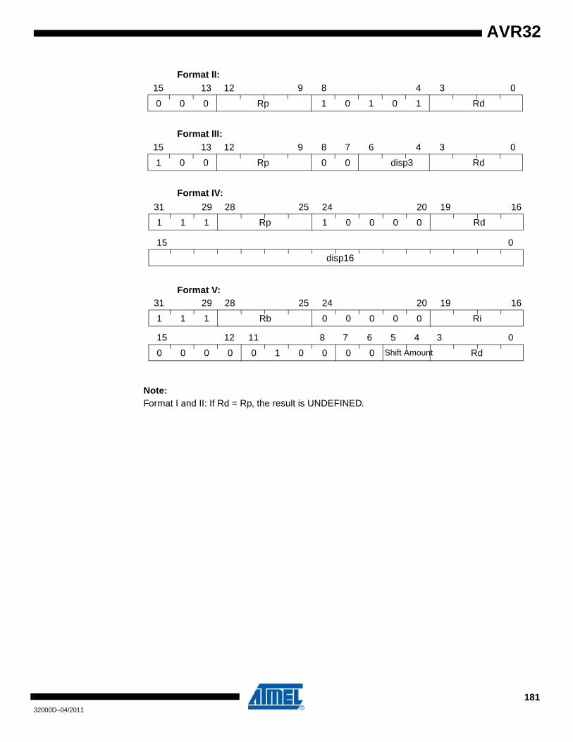
AVR32
Format II:
Format III:
Format IV:
Format V:
Note:Format I and II: If Rd = Rp, the result is UNDEFINED.
0 0 0 Rp 1 0 1 0 1 Rd
15 13 12 9 8 4 3 0
1 0 0 Rp 0 0 disp3 Rd
15 13 12 9 8 7 6 4 3 0
1 1 1 Rp 1 0 0 0 0 Rd
31 29 28 25 24 20 19 16
disp16
15 0
1 1 1 Rb 0 0 0 0 0 Ri
31 29 28 25 24 20 19 16
0 0 0 0 0 1 0 0 0 0 Shift Amount Rd
15 12 11 8 7 6 5 4 3 0
18132000D–04/2011
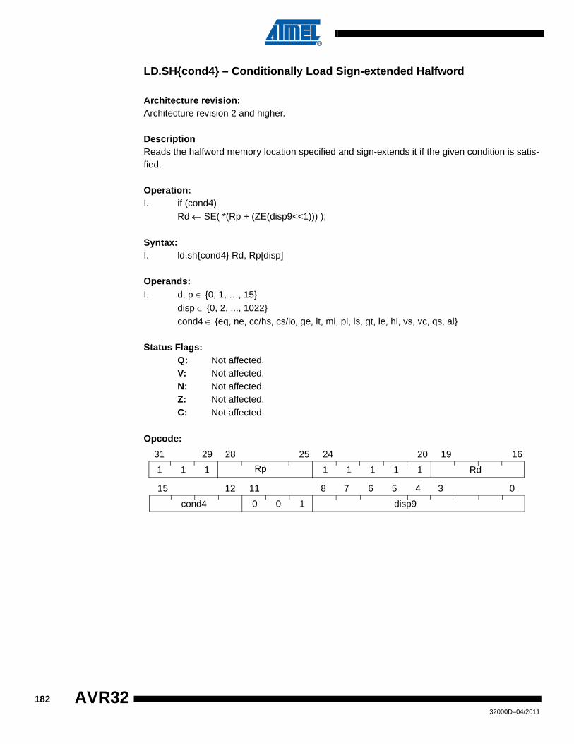
LD.SH{cond4} – Conditionally Load Sign-extended Halfword
Architecture revision: Architecture revision 2 and higher.
DescriptionReads the halfword memory location specified and sign-extends it if the given condition is satis-fied.
Operation:I. if (cond4)
Rd ← SE( *(Rp + (ZE(disp9<<1))) );
Syntax:I. ld.sh{cond4} Rd, Rp[disp]
Operands:I. d, p ∈ {0, 1, …, 15}
disp ∈ {0, 2, ..., 1022}cond4 ∈ {eq, ne, cc/hs, cs/lo, ge, lt, mi, pl, ls, gt, le, hi, vs, vc, qs, al}
Status Flags:Q: Not affected.V: Not affected.N: Not affected.Z: Not affected.C: Not affected.
Opcode:
1 1 1 1 1 1 1 1
31 29 28 25 24 20 19 16
cond4 0 0 1 disp9
15 12 11 8 7 6 5 4 3 0
RdRp
18232000D–04/2011
AVR32

AVR32
LD.UH – Load Zero-extended Halfword
Architecture revision:Architecture revision1 and higher.
DescriptionReads the halfword memory location specified and zero-extends it.
Operation:I. Rd ← ZE( *(Rp) );
Rp ← Rp + 2;II. Rp ← Rp - 2;
Rd ← ZE( *(Rp) );III. Rd ← ZE( *(Rp + (ZE(disp3) << 1)) );IV. Rd ← ZE( *(Rp + (SE(disp16))) );V. Rd ← ZE( *(Rb + (Ri << sa2)) );
Syntax:I. ld.uh Rd, Rp++II. ld.uh Rd, --RpIII. ld.uh Rd, Rp[disp]IV. ld.uh Rd, Rp[disp]V. ld.uh Rd, Rb[Ri<<sa]
Operands:I-V. d, p, b, i ∈ {0, 1, …, 15}III. disp ∈ {0, 2, ..., 14}IV. disp ∈ {-32768, -32767, ..., 32767}V. sa ∈ {0, 1, 2, 3}
Status Flags:Q: Not affected.V: Not affected.N: Not affected.Z: Not affected.C: Not affected.
Opcode:
Format I:
0 0 0 Rp 1 0 0 1 0 Rd
15 13 12 9 8 4 3 0
18332000D–04/2011
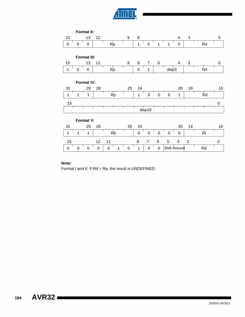
Format II:
Format III:
Format IV:
Format V:
Note:Format I and II: If Rd = Rp, the result is UNDEFINED.
0 0 0 Rp 1 0 1 1 0 Rd
15 13 12 9 8 4 3 0
1 0 0 Rp 0 1 disp3 Rd
15 13 12 9 8 7 6 4 3 0
1 1 1 Rp 1 0 0 0 1 Rd
31 29 28 25 24 20 19 16
disp16
15 0
1 1 1 Rb 0 0 0 0 0 Ri
31 29 28 25 24 20 19 16
0 0 0 0 0 1 0 1 0 0 Shift Amount Rd
15 12 11 8 7 6 5 4 3 0
18432000D–04/2011
AVR32
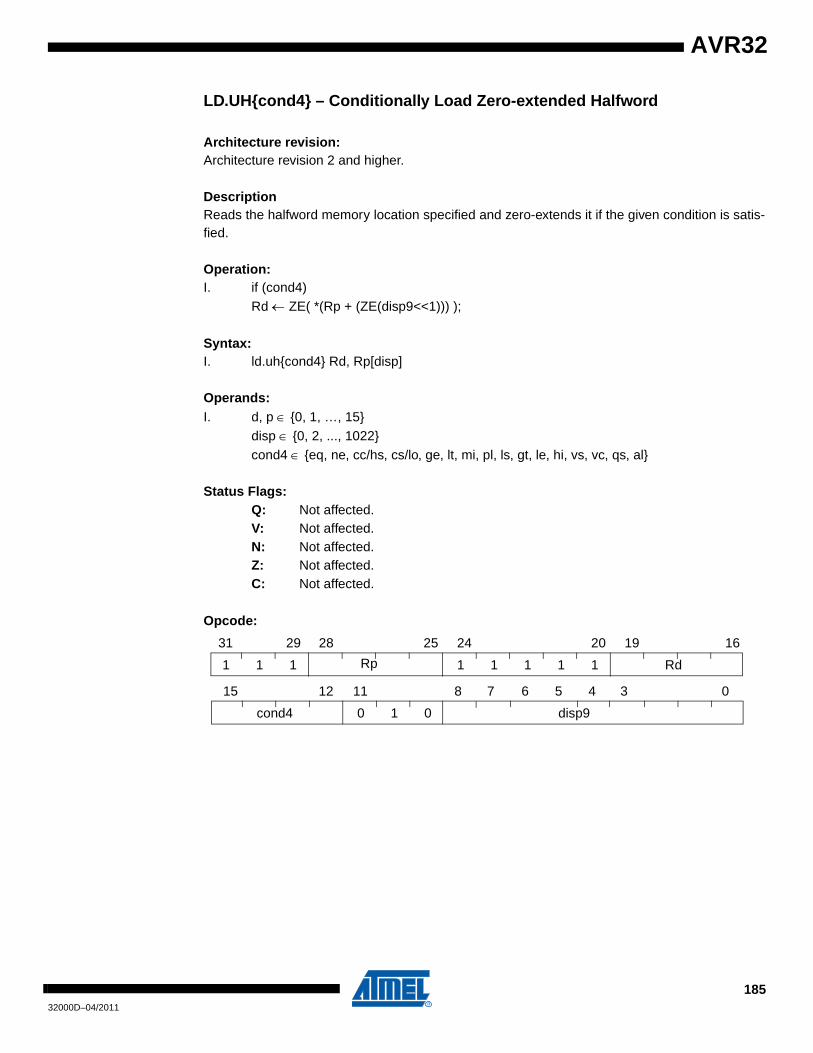
AVR32
LD.UH{cond4} – Conditionally Load Zero-extended Halfword
Architecture revision: Architecture revision 2 and higher.
DescriptionReads the halfword memory location specified and zero-extends it if the given condition is satis-fied.
Operation:I. if (cond4)
Rd ← ZE( *(Rp + (ZE(disp9<<1))) );
Syntax:I. ld.uh{cond4} Rd, Rp[disp]
Operands:I. d, p ∈ {0, 1, …, 15}
disp ∈ {0, 2, ..., 1022}cond4 ∈ {eq, ne, cc/hs, cs/lo, ge, lt, mi, pl, ls, gt, le, hi, vs, vc, qs, al}
Status Flags:Q: Not affected.V: Not affected.N: Not affected.Z: Not affected.C: Not affected.
Opcode:
1 1 1 1 1 1 1 1
31 29 28 25 24 20 19 16
cond4 0 1 0 disp9
15 12 11 8 7 6 5 4 3 0
RdRp
18532000D–04/2011

LD.W – Load Word
Architecture revision:Architecture revision1 and higher.
DescriptionFormat I to V: Reads the word memory location specified.Format VI: This instruction extracts a specified byte from Ri. This value is zero-extended, shifted left two positions and added to Rb to form an address. The contents of this address is loaded into Rd. The instruction is useful for indexing tables.
Operation:I. Rd ← *(Rp);
Rp ← Rp + 4;II. Rp ← Rp - 4;
Rd ← *(Rp);III. Rd ← *(Rp + (ZE(disp5) << 2));IV. Rd ← *(Rp + (SE(disp16)));V. Rd ← *(Rb + (Ri << sa2));VI. If (part == b)
Rd ← *(Rb + (Ri[7:0] << 2) );else if (part == l)
Rd ← *(Rb + (Ri[15:8] << 2) );else if (part == u)
Rd ← *(Rb + (Ri[23:16] << 2) );else
Rd ← *(Rb + (Ri[31:24] << 2) );
Syntax:I. ld.w Rd, Rp++II. ld.w Rd, --RpIII. ld.w Rd, Rp[disp]IV. ld.w Rd, Rp[disp]V. ld.w Rd, Rb[Ri<<sa]VI. ld.w Rd, Rb[Ri:<part> << 2]
Operands:I-V. d, p, b, i ∈ {0, 1, …, 15}III. disp ∈ {0, 4, ..., 124}IV. disp ∈ {-32768, -32767, ..., 32767}V. sa ∈ {0, 1, 2, 3}VI. {d, b, i} ∈ {0, 1, …, 15}
part ∈ {t, u, l, b}
18632000D–04/2011
AVR32
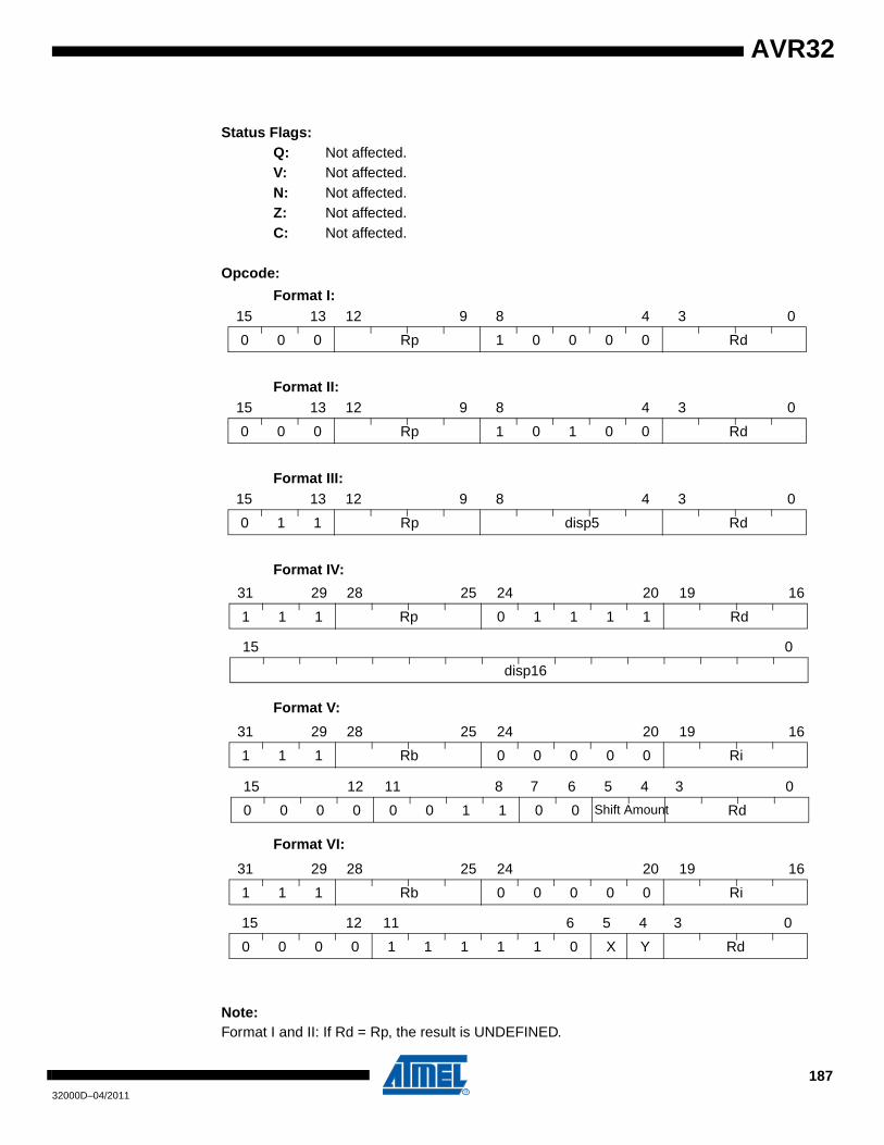
AVR32
Status Flags:Q: Not affected.V: Not affected.N: Not affected.Z: Not affected.C: Not affected.
Opcode:
Format I:
Format II:
Format III:
Format IV:
Format V:
Format VI:
Note:Format I and II: If Rd = Rp, the result is UNDEFINED.
0 0 0 Rp 1 0 0 0 0 Rd
15 13 12 9 8 4 3 0
0 0 0 Rp 1 0 1 0 0 Rd
15 13 12 9 8 4 3 0
0 1 1 Rp disp5 Rd
15 13 12 9 8 4 3 0
1 1 1 Rp 0 1 1 1 1 Rd
31 29 28 25 24 20 19 16
disp16
15 0
1 1 1 Rb 0 0 0 0 0 Ri
31 29 28 25 24 20 19 16
0 0 0 0 0 0 1 1 0 0 Shift Amount Rd
15 12 11 8 7 6 5 4 3 0
1 1 1 Rb 0 0 0 0 0 Ri
31 29 28 25 24 20 19 16
0 0 0 0 1 1 1 1 1 0 X Y Rd
15 12 11 6 5 4 3 0
18732000D–04/2011

18832000D–04/2011
AVR32

AVR32
LD.W{cond4} – Conditionally Load Word
Architecture revision: Architecture revision 2 and higher.
DescriptionReads the word memory location specified if the given condition is satisfied.
Operation:I. if (cond4)
Rd ← *(Rp + (ZE(disp9<<2)));
Syntax:I. ld.w{cond4} Rd, Rp[disp]
Operands:I. d, p ∈ {0, 1, …, 15}
disp ∈ {0, 4, ..., 2044}cond4 ∈ {eq, ne, cc/hs, cs/lo, ge, lt, mi, pl, ls, gt, le, hi, vs, vc, qs, al}
Status Flags:Q: Not affected.V: Not affected.N: Not affected.Z: Not affected.C: Not affected.
Opcode:
1 1 1 1 1 1 1 1
31 29 28 25 24 20 19 16
cond4 0 0 0 disp9
15 12 11 8 7 6 5 4 3 0
RdRp
18932000D–04/2011

LDC.{D,W} – Load Coprocessor
Architecture revision:Architecture revision1 and higher.
DescriptionReads the memory location specified into the addressed coprocessor.
Operation:I. CP#(CRd+1:CRd) ← *(Rp + (ZE(disp8) << 2));II. Rp ← Rp-8;
CP#(CRd+1:CRd) ← *(Rp);III. CP#(CRd+1:CRd) ← *(Rb + (Ri << sa2));IV. CP#(CRd) ← *(Rp + (ZE(disp8) << 2));V. Rp ← Rp-4;
CP#(CRd) ← *(Rp);VI. CP#(CRd) ← *(Rb + (Ri << sa2));
Syntax:I. ldc.d CP#, CRd, Rp[disp]II. ldc.d CP#, CRd, --RpIII. ldc.d CP#, CRd, Rb[Ri<<sa]IV. ldc.w CP#, CRd, Rp[disp]V. ldc.w CP#, CRd, --RpVI. ldc.w CP#, CRd, Rb[Ri<<sa]
Operands:I-VI. # ∈ {0, 1, …, 7}I-II, IV-V.p ∈ {0, 1, …, 15}I-III. d ∈ {0, 2, …, 14}I, IV. disp ∈ {0, 4, …, 1020}III, VI. {b, i} ∈ {0, 1, …, 15}III, VI. sa ∈ {0, 1, 2, 3}
Status Flags:Q: Not affected.V: Not affected.N: Not affected.Z: Not affected.C: Not affected.
Opcode:
19032000D–04/2011
AVR32
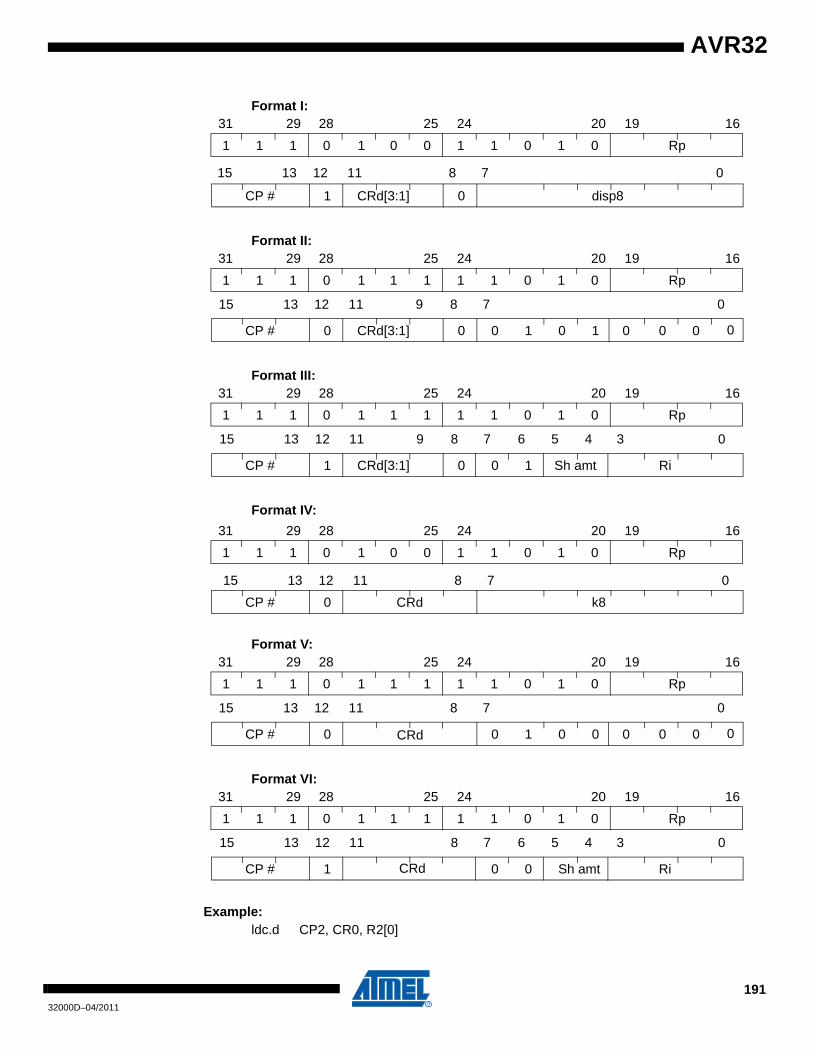
AVR32
Format I:
Format II:
Format III:
Format IV:
Format V:
Format VI:
Example:ldc.d CP2, CR0, R2[0]
1 1 1 0 0 0 1 1 0 1 0 Rp
31 29 28 25 24 20 19 16
CP # 1 CRd[3:1] 0 disp8
15 13 12 11 8 7 0
1
1 1 1 0 1 1 1 1 0 1 0 Rp
31 29 28 25 24 20 19 16
CP # 0 CRd[3:1] 0 0 1 0 1 0 0 0
15 13 12 11 9 8 7 0
1
0
1 1 1 0 1 1 1 1 0 1 0 Rp
31 29 28 25 24 20 19 16
CP # 1 CRd[3:1] 0 0 1 Sh amt Ri
15 13 12 11 9 8 7 6 5 4 3 0
1
1 1 1 0 0 0 1 1 0 1 0 Rp
31 29 28 25 24 20 19 16
CP # 0 CRd k8
15 13 12 11 8 7 0
1
1 1 1 0 1 1 1 1 0 1 0 Rp
31 29 28 25 24 20 19 16
CP # 0 0 1 0 0 0 0 0
15 13 12 11 8 7 0
1
0CRd
1 1 1 0 1 1 1 1 0 1 0 Rp
31 29 28 25 24 20 19 16
CP # 1 0 0 Sh amt Ri
15 13 12 11 8 7 6 5 4 3 0
1
CRd
19132000D–04/2011
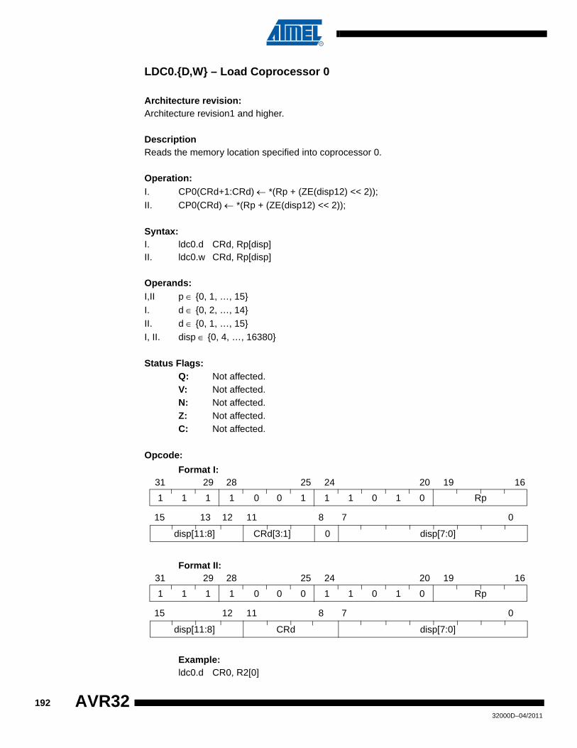
LDC0.{D,W} – Load Coprocessor 0
Architecture revision:Architecture revision1 and higher.
DescriptionReads the memory location specified into coprocessor 0.
Operation:I. CP0(CRd+1:CRd) ← *(Rp + (ZE(disp12) << 2));II. CP0(CRd) ← *(Rp + (ZE(disp12) << 2));
Syntax:I. ldc0.d CRd, Rp[disp]II. ldc0.w CRd, Rp[disp]
Operands:I,II p ∈ {0, 1, …, 15}I. d ∈ {0, 2, …, 14}II. d ∈ {0, 1, …, 15}I, II. disp ∈ {0, 4, …, 16380}
Status Flags:Q: Not affected.V: Not affected.N: Not affected.Z: Not affected.C: Not affected.
Opcode:
Format I:
Format II:
Example:ldc0.d CR0, R2[0]
1 1 1 1 0 1 1 1 0 1 0 Rp
31 29 28 25 24 20 19 16
disp[11:8] CRd[3:1] 0 disp[7:0]
15 13 12 11 8 7 0
0
1 1 1 1 0 0 1 1 0 1 0 Rp
31 29 28 25 24 20 19 16
disp[11:8] CRd disp[7:0]
15 12 11 8 7 0
0
19232000D–04/2011
AVR32

AVR32
LDCM.{D,W} – Load Coprocessor Multiple Registers
Architecture revision:Architecture revision1 and higher.
DescriptionReads the memory locations specified into the addressed coprocessor. The pointer register can optionally be updated after the operation.
Operation:I. Loadaddress ←Rp;
for (i = 7 to 0)if ReglistCPD8[i] == 1 then
CP#(CR(2*i+1)) ←*(Loadaddress++);CP#(CR(2*i)) ←*(Loadaddress++);
if Opcode[++] == 1 thenRp ← Loadaddress;
II. Loadaddress ←Rp;for (i = 7 to 0)
if ReglistCPH8[i] == 1 thenCP#(CRi+8) ←*(Loadaddress++);
if Opcode[++] == 1 thenRp ← Loadaddress;
III. Loadaddress ←Rp;for (i = 7 to 0)
if ReglistCPL8[i] == 1 thenCP#(CRi) ←*(Loadaddress++);
if Opcode[++] == 1 thenRp ← Loadaddress;
Syntax:I. ldcm.d CP#, Rp{++}, ReglistCPD8II. ldcm.w CP#, Rp{++}, ReglistCPH8 III. ldcm.w CP#, Rp{++}, ReglistCPL8
Operands:I-III. # ∈ {0, 1, …, 7}
p ∈ {0, 1, …, 15}I. ReglistCPD8 ∈ {CR0-CR1,CR2-CR3,CR4-CR5,CR6-CR7,CR8-CR9,
CR10-CR11,CR12-CR13,CR14-CR15}II. ReglistCPH8 ∈ {CR8, CR9, CR10, ..., CR15}III. ReglistCPL8 ∈ {CR0, CR1, CR2, ..., CR7}
19332000D–04/2011
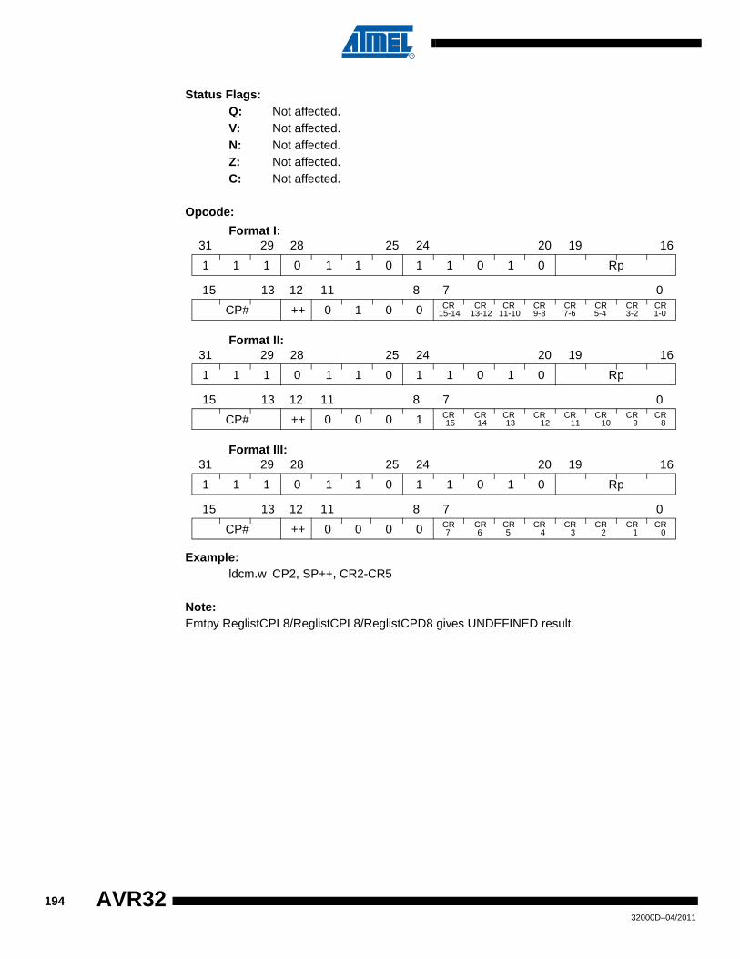
Status Flags:Q: Not affected.V: Not affected.N: Not affected.Z: Not affected.C: Not affected.
Opcode:
Format I:
Format II:
Format III:
Example:ldcm.w CP2, SP++, CR2-CR5
Note:Emtpy ReglistCPL8/ReglistCPL8/ReglistCPD8 gives UNDEFINED result.
1 1 1 0 1 0 1 1 0 1 0 Rp
31 29 28 25 24 20 19 16
CP# ++ 0 1 0 0 CR
15 13 12 11 8 7 0
1
15-14CR
13-12CR
11-10CR9-8
CR7-6
CR5-4
CR3-2
CR1-0
1 1 1 0 1 0 1 1 0 1 0 Rp
31 29 28 25 24 20 19 16
CP# ++ 0 0 0 1 CR
15 13 12 11 8 7 0
1
15CR
14CR
13CR 12
CR 11
CR 10
CR 9
CR 8
1 1 1 0 1 0 1 1 0 1 0 Rp
31 29 28 25 24 20 19 16
CP# ++ 0 0 0 0 CR
15 13 12 11 8 7 0
1
7CR
6CR
5CR 4
CR 3
CR 2
CR 1
CR 0
19432000D–04/2011
AVR32

AVR32
LDDPC – Load PC-relative with Displacement
Architecture revision:Architecture revision1 and higher.
DescriptionPerforms a PC relative load of a register
Operation:I. Rd ← *( (PC && 0xFFFF_FFFC) + (ZE(disp7) << 2));
Syntax:I. lddpc Rd, PC[disp]
Operands:I. d ∈ {0, 1, …, 15}
disp ∈ {0, 4, …, 508}
Status Flags:Q: Not affected.V: Not affected.N: Not affected.Z: Not affected.C: Not affected.
Opcode:
0 1 0 0 1 disp7 Rd
15 13 12 11 10 4 3 0
19532000D–04/2011
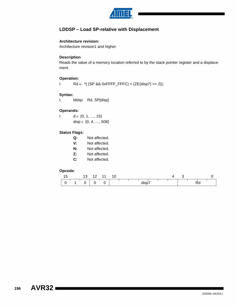
LDDSP – Load SP-relative with Displacement
Architecture revision:Architecture revision1 and higher.
DescriptionReads the value of a memory location referred to by the stack pointer register and a displace-ment.
Operation:I. Rd ← *( (SP && 0xFFFF_FFFC) + (ZE(disp7) << 2));
Syntax:I. lddsp Rd, SP[disp]
Operands:I. d ∈ {0, 1, …, 15}
disp ∈ {0, 4, …, 508}
Status Flags:Q: Not affected.V: Not affected.N: Not affected.Z: Not affected.C: Not affected.
Opcode:
0 1 0 0 0 disp7 Rd
15 13 12 11 10 4 3 0
19632000D–04/2011
AVR32
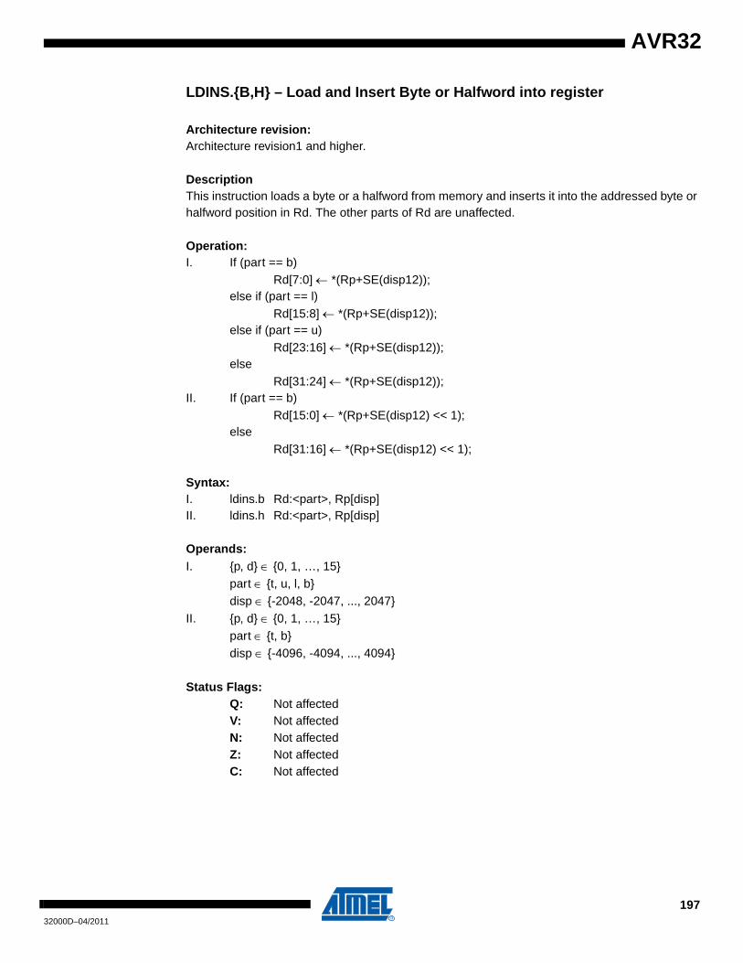
AVR32
LDINS.{B,H} – Load and Insert Byte or Halfword into register
Architecture revision:Architecture revision1 and higher.
DescriptionThis instruction loads a byte or a halfword from memory and inserts it into the addressed byte or halfword position in Rd. The other parts of Rd are unaffected.
Operation:I. If (part == b)
Rd[7:0] ← *(Rp+SE(disp12));else if (part == l)
Rd[15:8] ← *(Rp+SE(disp12));else if (part == u)
Rd[23:16] ← *(Rp+SE(disp12));else
Rd[31:24] ← *(Rp+SE(disp12));II. If (part == b)
Rd[15:0] ← *(Rp+SE(disp12) << 1);else
Rd[31:16] ← *(Rp+SE(disp12) << 1);
Syntax:I. ldins.b Rd:<part>, Rp[disp]II. ldins.h Rd:<part>, Rp[disp]
Operands:I. {p, d} ∈ {0, 1, …, 15}
part ∈ {t, u, l, b}disp ∈ {-2048, -2047, ..., 2047}
II. {p, d} ∈ {0, 1, …, 15}part ∈ {t, b}disp ∈ {-4096, -4094, ..., 4094}
Status Flags:Q: Not affectedV: Not affectedN: Not affectedZ: Not affectedC: Not affected
19732000D–04/2011

Opcode:
Format I:
Format II:
1 1 1 Rp 1 1 1 0 1 Rd
31 29 28 25 24 20 19 16
0 1 part disp12
15 14 13 12 11 0
1 1 1 Rp 1 1 1 0 1 Rd
31 29 28 25 24 20 19 16
0 0 0 part disp12
15 13 12 11 0
19832000D–04/2011
AVR32
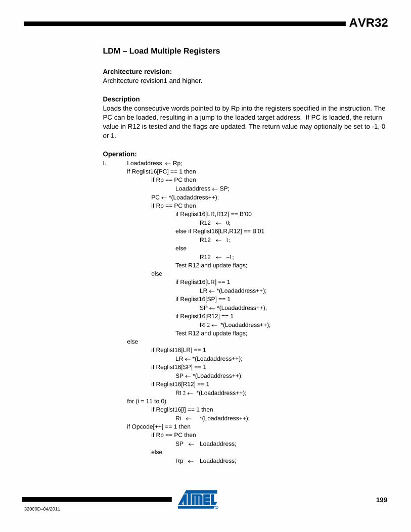
AVR32
LDM – Load Multiple Registers
Architecture revision:Architecture revision1 and higher.
DescriptionLoads the consecutive words pointed to by Rp into the registers specified in the instruction. The PC can be loaded, resulting in a jump to the loaded target address. If PC is loaded, the return value in R12 is tested and the flags are updated. The return value may optionally be set to -1, 0 or 1.
Operation:I. Loadaddress ← Rp;
if Reglist16[PC] == 1 then if Rp == PC then
Loadaddress ← SP;
PC ← *(Loadaddress++);if Rp == PC then
if Reglist16[LR,R12] == B’00
R12 ← 0;else if Reglist16[LR,R12] == B’01
R12 ← 1;else
R12 ← −1;Test R12 and update flags;
elseif Reglist16[LR] == 1
LR ← *(Loadaddress++);if Reglist16[SP] == 1
SP ← *(Loadaddress++);if Reglist16[R12] == 1
R12 ← *(Loadaddress++);Test R12 and update flags;
elseif Reglist16[LR] == 1
LR ← *(Loadaddress++);if Reglist16[SP] == 1
SP ← *(Loadaddress++);if Reglist16[R12] == 1
R12 ← *(Loadaddress++);for (i = 11 to 0)
if Reglist16[i] == 1 then
Ri ← *(Loadaddress++);if Opcode[++] == 1 then
if Rp == PC then
SP ← Loadaddress;else
Rp ← Loadaddress;
19932000D–04/2011
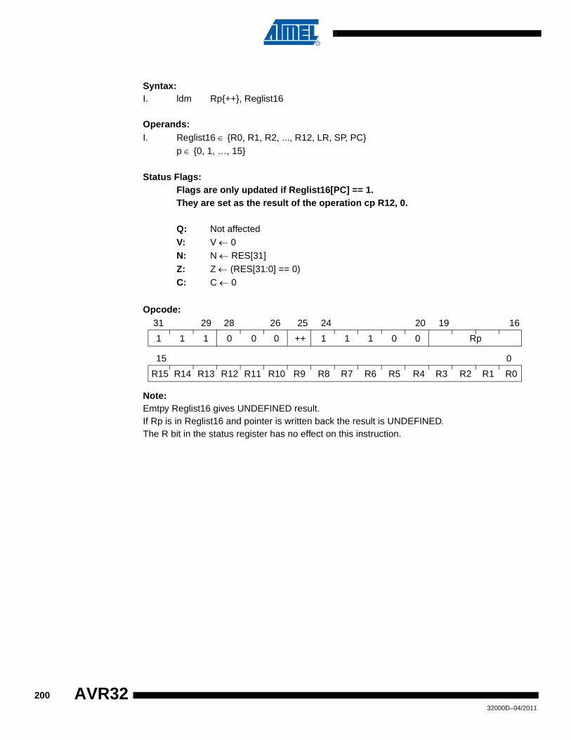
Syntax:I. ldm Rp{++}, Reglist16
Operands:I. Reglist16 ∈ {R0, R1, R2, ..., R12, LR, SP, PC}
p ∈ {0, 1, …, 15}
Status Flags:Flags are only updated if Reglist16[PC] == 1.They are set as the result of the operation cp R12, 0.
Q: Not affectedV: V ← 0N: N ← RES[31]Z: Z ← (RES[31:0] == 0)C: C ← 0
Opcode:
Note:Emtpy Reglist16 gives UNDEFINED result.If Rp is in Reglist16 and pointer is written back the result is UNDEFINED.The R bit in the status register has no effect on this instruction.
1 1 1 0 0 ++ 1 1 1 0 0 Rp
31 29 28 26 25 24 20 19 16
R15 R14 R13 R12 R11 R10 R9 R8 R7 R6 R5 R4 R3 R2 R1 R0
15 0
0
20032000D–04/2011
AVR32
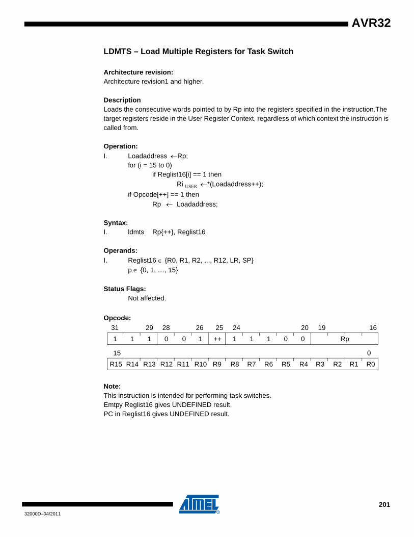
AVR32
LDMTS – Load Multiple Registers for Task Switch
Architecture revision:Architecture revision1 and higher.
DescriptionLoads the consecutive words pointed to by Rp into the registers specified in the instruction.The target registers reside in the User Register Context, regardless of which context the instruction is called from.
Operation:I. Loadaddress ←Rp;
for (i = 15 to 0)if Reglist16[i] == 1 then
Ri USER ←*(Loadaddress++);
if Opcode[++] == 1 thenRp ← Loadaddress;
Syntax:I. ldmts Rp{++}, Reglist16
Operands:I. Reglist16 ∈ {R0, R1, R2, ..., R12, LR, SP}
p ∈ {0, 1, …, 15}
Status Flags:Not affected.
Opcode:
Note:This instruction is intended for performing task switches.Emtpy Reglist16 gives UNDEFINED result.PC in Reglist16 gives UNDEFINED result.
1 1 1 0 1 ++ 1 1 1 0 0 Rp
31 29 28 26 25 24 20 19 16
R15 R14 R13 R12 R11 R10 R9 R8 R7 R6 R5 R4 R3 R2 R1 R0
15 0
0
20132000D–04/2011
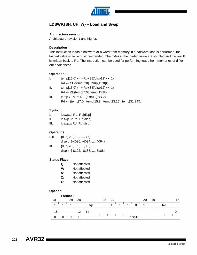
LDSWP.{SH, UH, W} – Load and Swap
Architecture revision:Architecture revision1 and higher.
DescriptionThis instruction loads a halfword or a word from memory. If a halfword load is performed, the loaded value is zero- or sign-extended. The bytes in the loaded value are shuffled and the result is written back to Rd. The instruction can be used for performing loads from memories of differ-ent endianness.
Operation:I. temp[15:0] ← *(Rp+SE(disp12) << 1);
Rd ← SE(temp[7:0], temp[15:8]);II. temp[15:0] ← *(Rp+SE(disp12) << 1);
Rd ← ZE(temp[7:0], temp[15:8]);III. temp ← *(Rp+SE(disp12) << 2);
Rd ← (temp[7:0], temp[15:8], temp[23:16], temp[31:24]);
Syntax:I. ldswp.shRd, Rp[disp]II. ldswp.uhRd, Rp[disp]III. ldswp.wRd, Rp[disp]
Operands:I, II. {d, p} ∈ {0, 1, …, 15}
disp ∈ {-4096, -4094, ..., 4094}III. {d, p} ∈ {0, 1, …, 15}
disp ∈ {-8192, -8188, ..., 8188}
Status Flags:Q: Not affectedV: Not affectedN: Not affectedZ: Not affectedC: Not affected
Opcode:
Format I:
1 1 1 Rp 1 1 1 0 1 Rd
31 29 28 25 24 20 19 16
0 0 1 0 disp12
15 12 11 0
20232000D–04/2011
AVR32
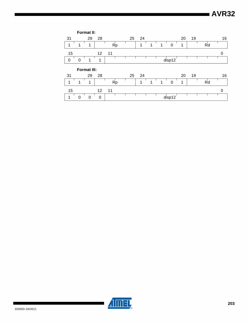
AVR32
Format II:
Format III:
1 1 1 Rp 1 1 1 0 1 Rd
31 29 28 25 24 20 19 16
0 0 1 1 disp12
15 12 11 0
1 1 1 Rp 1 1 1 0 1 Rd
31 29 28 25 24 20 19 16
1 0 0 0 disp12
15 12 11 0
20332000D–04/2011
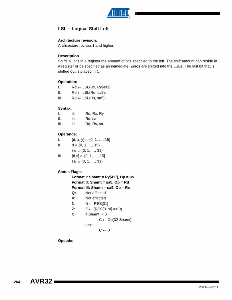
LSL – Logical Shift Left
Architecture revision:Architecture revision1 and higher.
DescriptionShifts all bits in a register the amount of bits specified to the left. The shift amount can reside in a register or be specified as an immediate. Zeros are shifted into the LSBs. The last bit that is shifted out is placed in C.
Operation:I. Rd ← LSL(Rx, Ry[4:0]);II. Rd ← LSL(Rd, sa5);III. Rd ← LSL(Rs, sa5);
Syntax:I. lsl Rd, Rx, RyII. lsl Rd, saIII. lsl Rd, Rs, sa
Operands:I. {d, x, y} ∈ {0, 1, …, 15}II. d ∈ {0, 1, …, 15}
sa ∈ {0, 1, …, 31}III. {d,s} ∈ {0, 1, …, 15}
sa ∈ {0, 1, …, 31}
Status Flags:Format I: Shamt = Ry[4:0], Op = RxFormat II: Shamt = sa5, Op = RdFormat III: Shamt = sa5, Op = RsQ: Not affectedV: Not affectedN: N ← RES[31]Z: Z ← (RES[31:0] == 0)C: if Shamt != 0
C ← Op[32-Shamt]else
C ← 0
Opcode:
20432000D–04/2011
AVR32
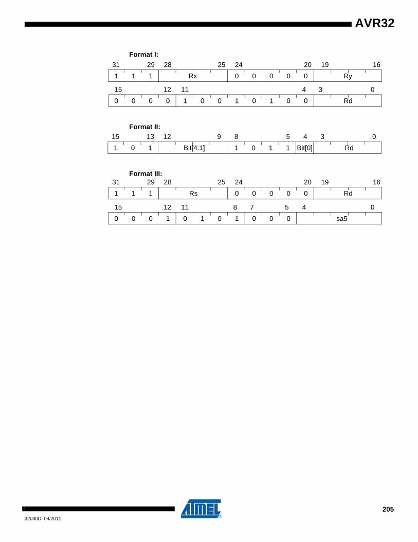
AVR32
Format I:
Format II:
Format III:
1 1 1 Rx 0 0 0 0 0 Ry
31 29 28 25 24 20 19 16
0 0 0 0 1 0 0 1 0 1 0 0 Rd
15 12 11 4 3 0
1 0 1 Bit[4:1] 1 0 1 1 Bit[0] Rd
15 13 12 9 8 5 4 3 0
1 1 1 Rs 0 0 0 0 0 Rd
31 29 28 25 24 20 19 16
0 0 0 1 0 1 0 1 0 0 0 sa5
15 12 11 8 7 5 4 0
20532000D–04/2011

LSR – Logical Shift Right
Architecture revision:Architecture revision1 and higher.
DescriptionShifts all bits in a register the amount specified to the right. The shift amount may be specified by a register or an immediate. Zeros are shifted into the MSB.
Operation:I. Rd ← LSR(Rx, Ry[4:0]);II. Rd ← LSR(Rd, sa5);III. Rd ← LSR(Rs, sa5);
Syntax:I. lsr Rd, Rx, RyII. lsr Rd, saIII. lsr Rd, Rs, sa
Operands: I. {d, x, y} ∈ {0, 1, …, 15}II. d ∈ {0, 1, …, 15}
sa ∈ {0, 1, …, 31}III. {d,s} ∈ {0, 1, …, 15}
sa ∈ {0, 1, …, 31}
Status Flags:Format I: Shamt = Ry[4:0], Op = RxFormat II: Shamt = sa5, Op = RdFormat III: Shamt = sa5, Op = RsQ: Not affectedV: Not affectedN: N ← RES[31]Z: Z ← (RES[31:0] == 0)C: if Shamt != 0
C ← Op[Shamt-1]else
C ← 0
20632000D–04/2011
AVR32
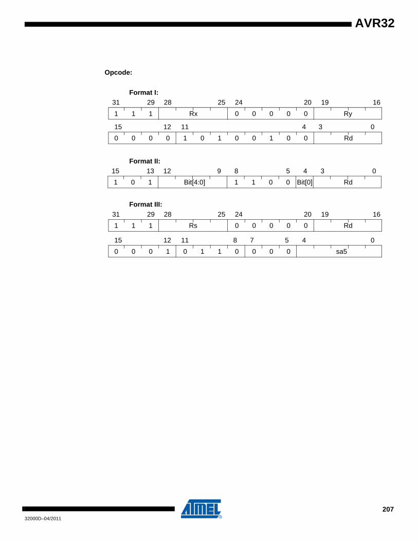
AVR32
Opcode:
Format I:
Format II:
Format III:
1 1 1 Rx 0 0 0 0 0 Ry
31 29 28 25 24 20 19 16
0 0 0 0 1 0 1 0 0 1 0 0 Rd
15 12 11 4 3 0
1 0 1 Bit[4:0] 1 1 0 0 Bit[0] Rd
15 13 12 9 8 5 4 3 0
1 1 1 Rs 0 0 0 0 0 Rd
31 29 28 25 24 20 19 16
0 0 0 1 0 1 1 0 0 0 0 sa5
15 12 11 8 7 5 4 0
20732000D–04/2011
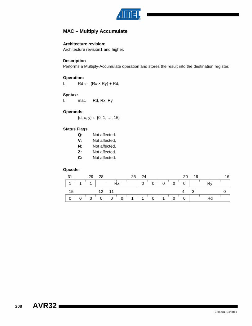
MAC – Multiply Accumulate
Architecture revision:Architecture revision1 and higher.
DescriptionPerforms a Multiply-Accumulate operation and stores the result into the destination register.
Operation:I. Rd ← (Rx × Ry) + Rd;
Syntax:I. mac Rd, Rx, Ry
Operands:{d, x, y} ∈ {0, 1, …, 15}
Status FlagsQ: Not affected.V: Not affected.N: Not affected.Z: Not affected.C: Not affected.
Opcode:
1 1 1 Rx 0 0 0 0 0 Ry
31 29 28 25 24 20 19 16
0 0 0 0 0 0 1 1 0 1 0 0 Rd
15 12 11 4 3 0
20832000D–04/2011
AVR32

AVR32
MACHH.D – Multiply Halfwords and Accumulate in Doubleword
Architecture revision:Architecture revision1 and higher.
DescriptionMultiplies the two halfword registers specified and adds the result to the specified doubleword-register. Only the 48 highest of the 64 possible bits in the doubleword accumulator are used. The 16 lowest bits are cleared. The halfword registers are selected as either the high or low part of the operand registers.
Operation:I. If (Rx-part == t) then operand1 = SE(Rx[31:16]) else operand1 = SE(Rx[15:0]);
If (Ry-part == t) then operand2 = SE(Ry[31:16]) else operand2 = SE(Ry[15:0]);(Rd+1:Rd)[63:16] ← (operand1 × operand2)[31:0] + (Rd+1:Rd)[63:16];Rd[15:0] ← 0;
Syntax:I. machh.d Rd, Rx:<part>, Ry:<part>
Operands:I. d ∈ {0, 2, 4, …, 14}
{x, y} ∈ {0, 1, …, 15}part ∈ {t,b}
Status Flags:Q: Not affected.V: Not affected.N: Not affected.Z: Not affected.C: Not affected.
Opcode:
Example:machh.d R10, R2:t, R3:b will perform (R11 : R10)[63:16] ← ( SE(R2[31:16]) × SE(R3[15:0]) ) + (R11 : R10)[63:16]R10[15:0] ← 0
1 1 1 Rx 0 0 0 0 0 Ry
31 29 28 25 24 20 19 16
0 0 0 0 0 1 0 1 1 0 X Y Rd
15 12 11 8 7 6 5 4 3 0
20932000D–04/2011
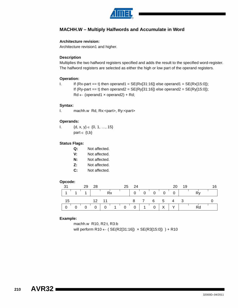
MACHH.W – Multiply Halfwords and Accumulate in Word
Architecture revision:Architecture revision1 and higher.
DescriptionMultiplies the two halfword registers specified and adds the result to the specified word-register. The halfword registers are selected as either the high or low part of the operand registers.
Operation:I. If (Rx-part == t) then operand1 = SE(Rx[31:16]) else operand1 = SE(Rx[15:0]);
If (Ry-part == t) then operand2 = SE(Ry[31:16]) else operand2 = SE(Ry[15:0]);Rd ← (operand1 × operand2) + Rd;
Syntax:I. machh.w Rd, Rx:<part>, Ry:<part>
Operands:I. {d, x, y} ∈ {0, 1, …, 15}
part ∈ {t,b}
Status Flags:Q: Not affected.V: Not affected.N: Not affected.Z: Not affected.C: Not affected.
Opcode:
Example:machh.w R10, R2:t, R3:bwill perform R10 ← ( SE(R2[31:16]) × SE(R3[15:0]) ) + R10
1 1 1 Rx 0 0 0 0 0 Ry
31 29 28 25 24 20 19 16
0 0 0 0 0 1 0 0 1 0 X Y Rd
15 12 11 8 7 6 5 4 3 0
21032000D–04/2011
AVR32
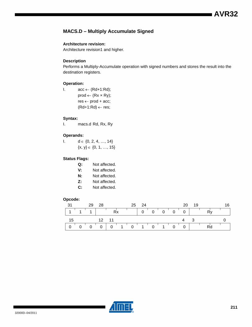
AVR32
MACS.D – Multiply Accumulate Signed
Architecture revision:Architecture revision1 and higher.
DescriptionPerforms a Multiply-Accumulate operation with signed numbers and stores the result into the destination registers.
Operation:I. acc ← (Rd+1:Rd);
prod ← (Rx × Ry);res ← prod + acc;(Rd+1:Rd) ← res;
Syntax:I. macs.d Rd, Rx, Ry
Operands:I. d ∈ {0, 2, 4, …, 14}
{x, y} ∈ {0, 1, …, 15}
Status Flags:Q: Not affected.V: Not affected.N: Not affected.Z: Not affected.C: Not affected.
Opcode:
1 1 1 Rx 0 0 0 0 0 Ry
31 29 28 25 24 20 19 16
0 0 0 0 0 1 0 1 0 1 0 0 Rd
15 12 11 4 3 0
21132000D–04/2011
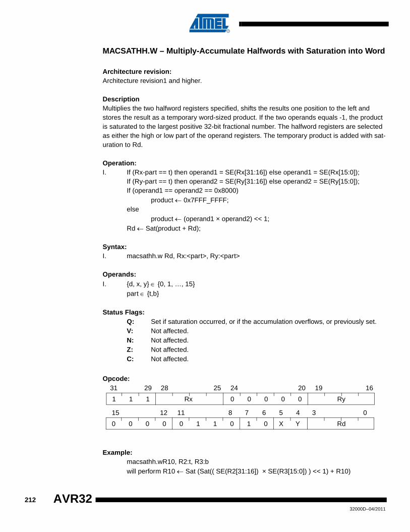
MACSATHH.W – Multiply-Accumulate Halfwords with Saturation into Word
Architecture revision:Architecture revision1 and higher.
DescriptionMultiplies the two halfword registers specified, shifts the results one position to the left and stores the result as a temporary word-sized product. If the two operands equals -1, the product is saturated to the largest positive 32-bit fractional number. The halfword registers are selected as either the high or low part of the operand registers. The temporary product is added with sat-uration to Rd.
Operation:I. If (Rx-part == t) then operand1 = SE(Rx[31:16]) else operand1 = SE(Rx[15:0]);
If (Ry-part == t) then operand2 = SE(Ry[31:16]) else operand2 = SE(Ry[15:0]);If (operand1 == operand2 == 0x8000)
product ← 0x7FFF_FFFF;else
product ← (operand1 × operand2) << 1;Rd ← Sat(product + Rd);
Syntax:I. macsathh.w Rd, Rx:<part>, Ry:<part>
Operands:I. {d, x, y} ∈ {0, 1, …, 15}
part ∈ {t,b}
Status Flags:Q: Set if saturation occurred, or if the accumulation overflows, or previously set.V: Not affected.N: Not affected.Z: Not affected.C: Not affected.
Opcode:
Example:macsathh.wR10, R2:t, R3:bwill perform R10 ← Sat (Sat(( SE(R2[31:16]) × SE(R3[15:0]) ) << 1) + R10)
1 1 1 Rx 0 0 0 0 0 Ry
31 29 28 25 24 20 19 16
0 0 0 0 0 1 1 0 1 0 X Y Rd
15 12 11 8 7 6 5 4 3 0
21232000D–04/2011
AVR32

AVR32
MACU.D – Multiply Accumulate Unsigned
Architecture revision:Architecture revision1 and higher.
DescriptionPerforms a Multiply-Accumulate operation with unsigned numbers and stores the result into the destination registers.
Operation:I. acc ← (Rd+1:Rd);
prod ← (Rx × Ry);res ← prod + acc;(Rd+1:Rd) ← res;
Syntax:I. macu.d Rd, Rx, Ry
Operands:I. d ∈ {0, 2, 4, …, 14}
{x, y} ∈ {0, 1, …, 15}
Status FlagsQ: Not affected.V: Not affected.N: Not affected.Z: Not affected.C: Not affected.
Opcode:
1 1 1 Rx 0 0 0 0 0 Ry
31 29 28 25 24 20 19 16
0 0 0 0 0 1 1 1 0 1 0 0 Rd
15 12 11 4 3 0
21332000D–04/2011
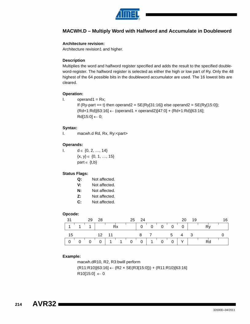
MACWH.D – Multiply Word with Halfword and Accumulate in Doubleword
Architecture revision:Architecture revision1 and higher.
DescriptionMultiplies the word and halfword register specified and adds the result to the specified double-word-register. The halfword register is selected as either the high or low part of Ry. Only the 48 highest of the 64 possible bits in the doubleword accumulator are used. The 16 lowest bits are cleared.
Operation:I. operand1 = Rx;
If (Ry-part == t) then operand2 = SE(Ry[31:16]) else operand2 = SE(Ry[15:0]);(Rd+1:Rd)[63:16] ← (operand1 × operand2)[47:0] + (Rd+1:Rd)[63:16];Rd[15:0] ← 0;
Syntax:I. macwh.d Rd, Rx, Ry:<part>
Operands:I. d ∈ {0, 2, …, 14}
{x, y} ∈ {0, 1, …, 15}part ∈ {t,b}
Status Flags:Q: Not affected.V: Not affected.N: Not affected.Z: Not affected.C: Not affected.
Opcode:
Example:macwh.dR10, R2, R3:bwill perform (R11:R10)[63:16] ← (R2 × SE(R3[15:0])) + (R11:R10)[63:16]R10[15:0] ← 0
1 1 1 Rx 0 0 0 0 0 Ry
31 29 28 25 24 20 19 16
0 0 0 0 1 1 0 0 1 0 0 Y Rd
15 12 11 8 7 5 4 3 0
21432000D–04/2011
AVR32
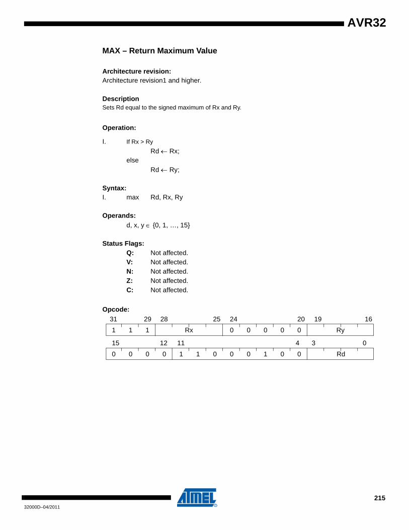
AVR32
MAX – Return Maximum Value
Architecture revision:Architecture revision1 and higher.
DescriptionSets Rd equal to the signed maximum of Rx and Ry.
Operation:
I. If Rx > Ry
Rd ← Rx;else
Rd ← Ry;
Syntax:I. max Rd, Rx, Ry
Operands: d, x, y ∈ {0, 1, …, 15}
Status Flags:Q: Not affected.V: Not affected.N: Not affected.Z: Not affected.C: Not affected.
Opcode:
1 1 1 Rx 0 0 0 0 0 Ry
31 29 28 25 24 20 19 16
0 0 0 0 1 1 0 0 0 1 0 0 Rd
15 12 11 4 3 0
21532000D–04/2011
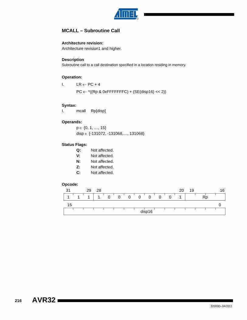
MCALL – Subroutine Call
Architecture revision:Architecture revision1 and higher.
DescriptionSubroutine call to a call destination specified in a location residing in memory.
Operation:
I. LR ← PC + 4
PC ← *((Rp & 0xFFFFFFFC) + (SE(disp16) << 2))
Syntax:I. mcall Rp[disp]
Operands: p ∈ {0, 1, …, 15}disp ∈ {-131072, -131068,…, 131068}
Status Flags:Q: Not affected.V: Not affected.N: Not affected.Z: Not affected.C: Not affected.
Opcode:
1 1 1 1 0 0 0 0 0 0 0 1 Rp
31 29 28 20 19 16
disp16
15 0
21632000D–04/2011
AVR32
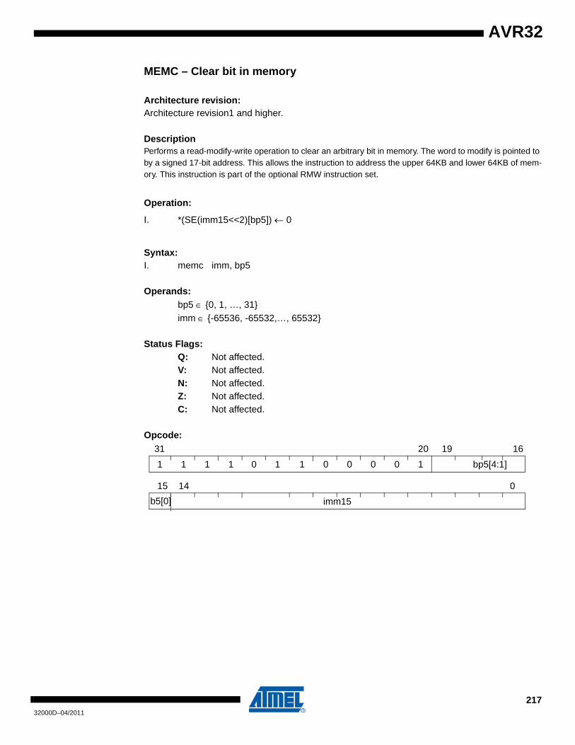
AVR32
MEMC – Clear bit in memory
Architecture revision:Architecture revision1 and higher.
DescriptionPerforms a read-modify-write operation to clear an arbitrary bit in memory. The word to modify is pointed to by a signed 17-bit address. This allows the instruction to address the upper 64KB and lower 64KB of mem-ory. This instruction is part of the optional RMW instruction set.
Operation:
I. *(SE(imm15<<2)[bp5]) ← 0
Syntax:I. memc imm, bp5
Operands: bp5 ∈ {0, 1, …, 31}imm ∈ {-65536, -65532,…, 65532}
Status Flags:Q: Not affected.V: Not affected.N: Not affected.Z: Not affected.C: Not affected.
Opcode:
1 1 1 1 1 1 0 0 0 0 1 bp5[4:1]
31 20 19 16
b5[0] imm15
15 14 0
0
21732000D–04/2011
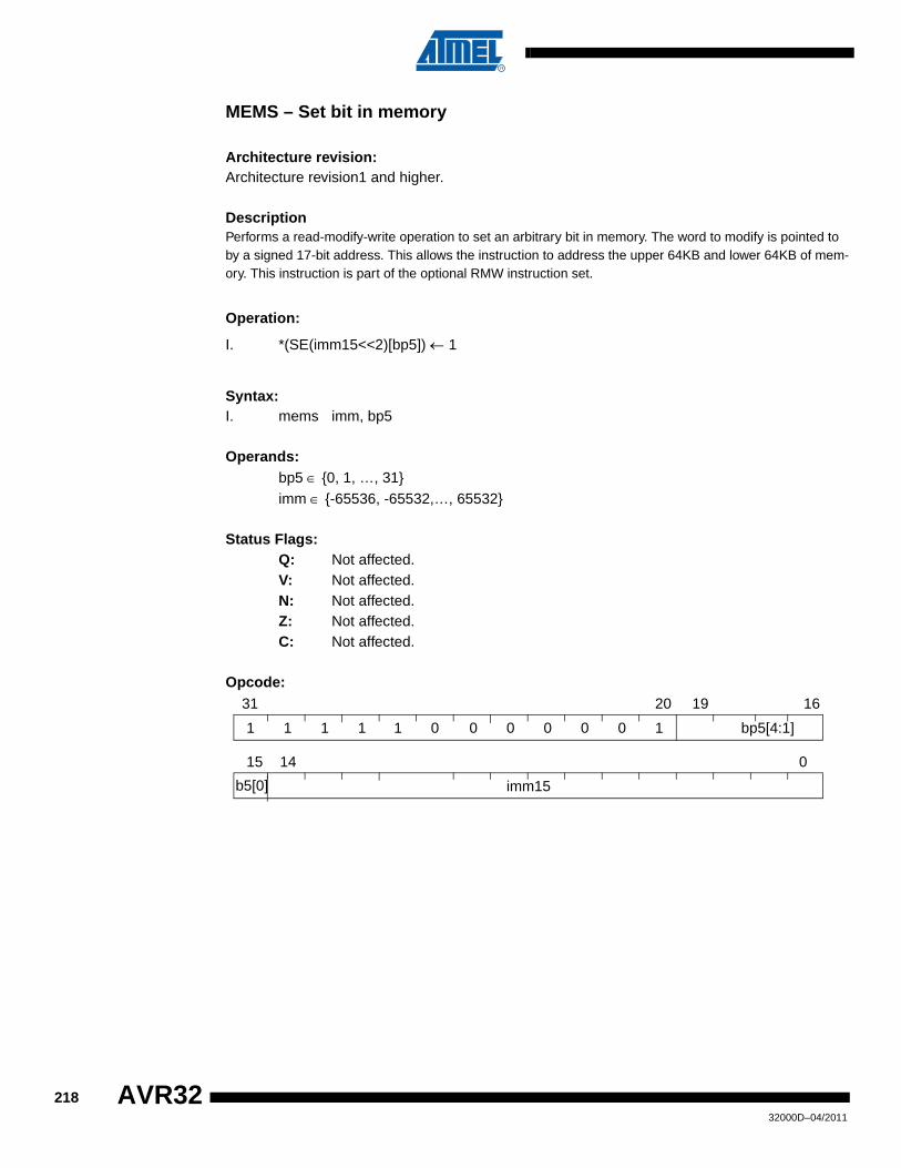
MEMS – Set bit in memory
Architecture revision:Architecture revision1 and higher.
DescriptionPerforms a read-modify-write operation to set an arbitrary bit in memory. The word to modify is pointed to by a signed 17-bit address. This allows the instruction to address the upper 64KB and lower 64KB of mem-ory. This instruction is part of the optional RMW instruction set.
Operation:
I. *(SE(imm15<<2)[bp5]) ← 1
Syntax:I. mems imm, bp5
Operands: bp5 ∈ {0, 1, …, 31}imm ∈ {-65536, -65532,…, 65532}
Status Flags:Q: Not affected.V: Not affected.N: Not affected.Z: Not affected.C: Not affected.
Opcode:
1 1 1 1 0 0 0 0 0 0 1 bp5[4:1]
31 20 19 16
b5[0] imm15
15 14 0
1
21832000D–04/2011
AVR32

AVR32
MEMT – Toggle bit in memory
Architecture revision:Architecture revision1 and higher.
DescriptionPerforms a read-modify-write operation to toggle an arbitrary bit in memory. The word to modifyis pointed to by a signed 17-bit address. This allows the instruction to address the upper 64KBand lower 64KB of memory. This instruction is part of the optional RMW instruction set.
Operation:
I. *(SE(imm15<<2)[bp5]) ← ¬*(SE(k15<<2)[bp5])
Syntax:I. memt imm, bp5
Operands: bp5 ∈ {0, 1, …, 31}imm ∈ {-65536, -65532,…, 65532}
Status Flags:Q: Not affected.V: Not affected.N: Not affected.Z: Not affected.C: Not affected.
Opcode:
1 1 1 1 0 1 0 0 0 0 1 bp5[4:1]
31 20 19 16
b5[0] imm15
15 14 0
1
21932000D–04/2011

MFDR – Move from Debug Register
Architecture revision:Architecture revision1 and higher.
DescriptionThe instruction copies the value in the specified debug register to the specified register in the register file. Note that special timing concerns must be considered when operating on the debug registers, see the Pipeline Chapter for details.
Operation:I. Rd ← DebugRegister[DebugRegisterAddress << 2];
Syntax:I. mfdr Rd, DebugRegisterNo
Operands:I. DebugRegisterNo ∈ {0, 4, 8, ..., 1020}
Status Flags:Q: Not affected.V: Not affected.N: Not affected.Z: Not affected.C: Not affected.
Opcode:
Note: Debug registers are implementation defined. If accessing a debug register that does not exist,the result is UNDEFINED.
This instruction can only be executed in a privileged mode. Execution from any other mode willtrigger a Privilege Violation exception.
1 1 1 0 0 1 0 1 1 0 1 1 Rd
31 20 19 16
0 0 0 0 0 0 0 0 Debug Register Ad-
15 8 7 0
22032000D–04/2011
AVR32
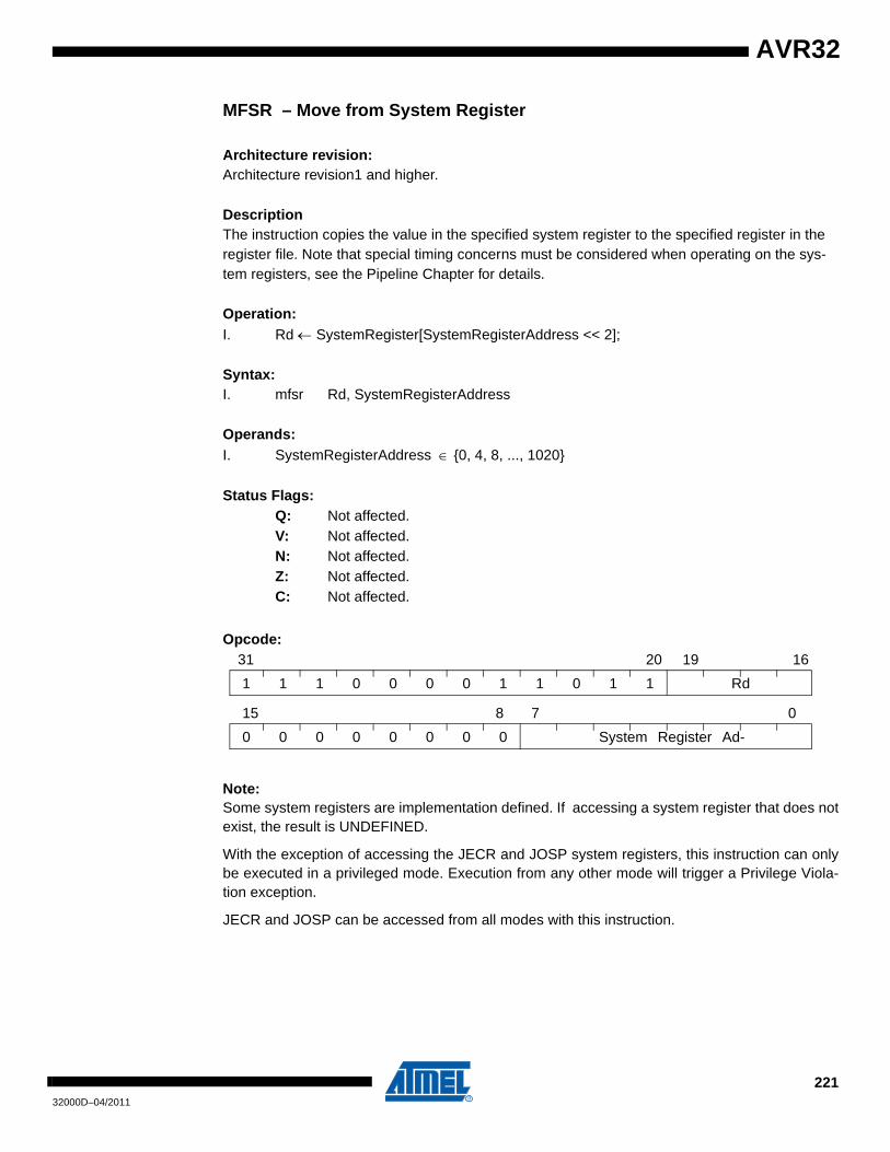
AVR32
MFSR – Move from System Register
Architecture revision:Architecture revision1 and higher.
DescriptionThe instruction copies the value in the specified system register to the specified register in the register file. Note that special timing concerns must be considered when operating on the sys-tem registers, see the Pipeline Chapter for details.
Operation:I. Rd ← SystemRegister[SystemRegisterAddress << 2];
Syntax:I. mfsr Rd, SystemRegisterAddress
Operands:I. SystemRegisterAddress ∈ {0, 4, 8, ..., 1020}
Status Flags:Q: Not affected.V: Not affected.N: Not affected.Z: Not affected.C: Not affected.
Opcode:
Note: Some system registers are implementation defined. If accessing a system register that does notexist, the result is UNDEFINED.
With the exception of accessing the JECR and JOSP system registers, this instruction can onlybe executed in a privileged mode. Execution from any other mode will trigger a Privilege Viola-tion exception.
JECR and JOSP can be accessed from all modes with this instruction.
1 1 1 0 0 0 0 1 1 0 1 1 Rd
31 20 19 16
0 0 0 0 0 0 0 0 System Register Ad-
15 8 7 0
22132000D–04/2011
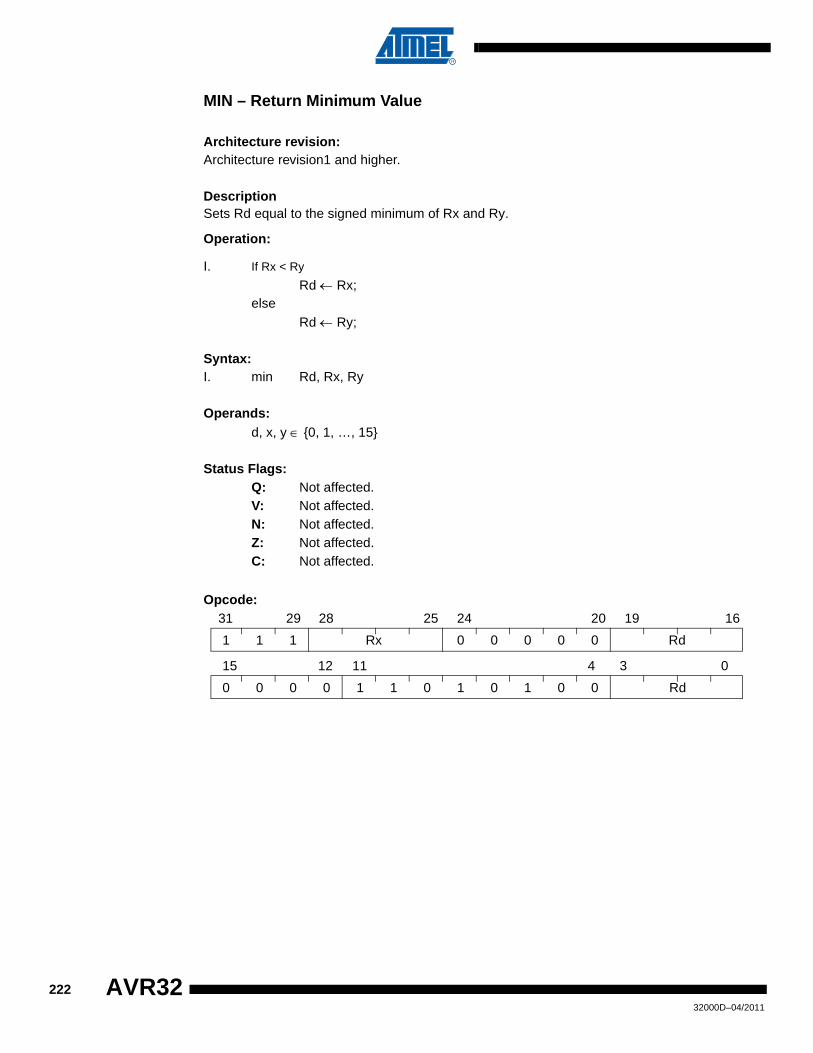
MIN – Return Minimum Value
Architecture revision:Architecture revision1 and higher.
DescriptionSets Rd equal to the signed minimum of Rx and Ry.
Operation:
I. If Rx < Ry
Rd ← Rx;else
Rd ← Ry;
Syntax:I. min Rd, Rx, Ry
Operands: d, x, y ∈ {0, 1, …, 15}
Status Flags:Q: Not affected.V: Not affected.N: Not affected.Z: Not affected.C: Not affected.
Opcode:
1 1 1 Rx 0 0 0 0 0 Rd
31 29 28 25 24 20 19 16
0 0 0 0 1 1 0 1 0 1 0 0 Rd
15 12 11 4 3 0
22232000D–04/2011
AVR32
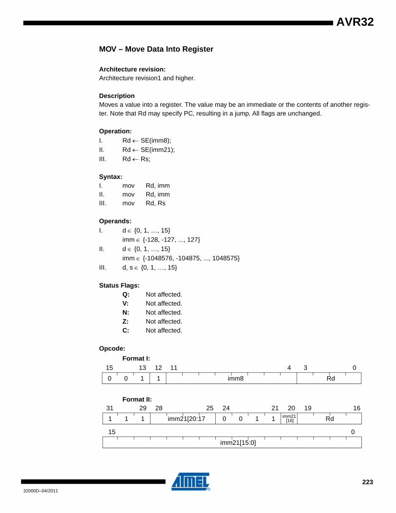
AVR32
MOV – Move Data Into Register
Architecture revision:Architecture revision1 and higher.
DescriptionMoves a value into a register. The value may be an immediate or the contents of another regis-ter. Note that Rd may specify PC, resulting in a jump. All flags are unchanged.
Operation:I. Rd ← SE(imm8);II. Rd ← SE(imm21);III. Rd ← Rs;
Syntax:I. mov Rd, immII. mov Rd, immIII. mov Rd, Rs
Operands:I. d ∈ {0, 1, …, 15}
imm ∈ {-128, -127, ..., 127}II. d ∈ {0, 1, …, 15}
imm ∈ {-1048576, -104875, ..., 1048575}III. d, s ∈ {0, 1, …, 15}
Status Flags:Q: Not affected.V: Not affected.N: Not affected.Z: Not affected.C: Not affected.
Opcode:
Format I:
Format II:
0 0 1 1 imm8 Rd
15 13 12 11 4 3 0
1 1 1 imm21[20:17 0 0 1 1 imm21 Rd
31 29 28 25 24 21 20 19 16
imm21[15:0]
15 0
[16]
22332000D–04/2011

Format III:
0 0 0 Rs 0 1 0 0 1 Rd
15 13 12 9 8 4 3 0
22432000D–04/2011
AVR32
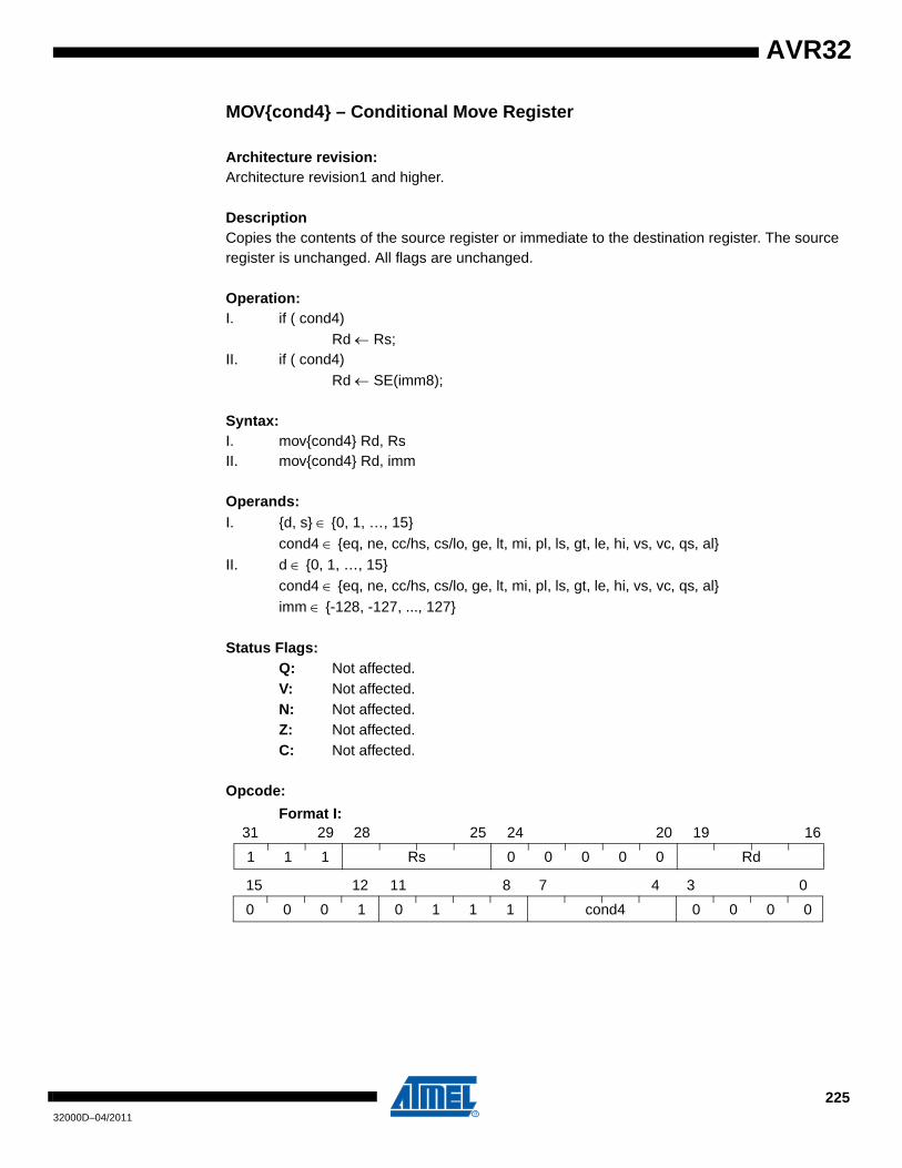
AVR32
MOV{cond4} – Conditional Move Register
Architecture revision:Architecture revision1 and higher.
DescriptionCopies the contents of the source register or immediate to the destination register. The source register is unchanged. All flags are unchanged.
Operation:I. if ( cond4)
Rd ← Rs;II. if ( cond4)
Rd ← SE(imm8);
Syntax:I. mov{cond4} Rd, RsII. mov{cond4} Rd, imm
Operands:I. {d, s} ∈ {0, 1, …, 15}
cond4 ∈ {eq, ne, cc/hs, cs/lo, ge, lt, mi, pl, ls, gt, le, hi, vs, vc, qs, al}II. d ∈ {0, 1, …, 15}
cond4 ∈ {eq, ne, cc/hs, cs/lo, ge, lt, mi, pl, ls, gt, le, hi, vs, vc, qs, al}imm ∈ {-128, -127, ..., 127}
Status Flags:Q: Not affected.V: Not affected.N: Not affected.Z: Not affected.C: Not affected.
Opcode:
Format I:
1 1 1 Rs 0 0 0 0 0 Rd
31 29 28 25 24 20 19 16
0 0 0 1 0 1 1 1 cond4 0 0 0 0
15 12 11 8 7 4 3 0
22532000D–04/2011
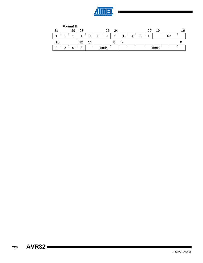
Format II:
1 1 1 1 0 0 1 1 0 1 1 Rd
31 29 28 25 24 20 19 16
0 0 0 0 cond4 imm8
15 12 11 8 7 0
1
22632000D–04/2011
AVR32
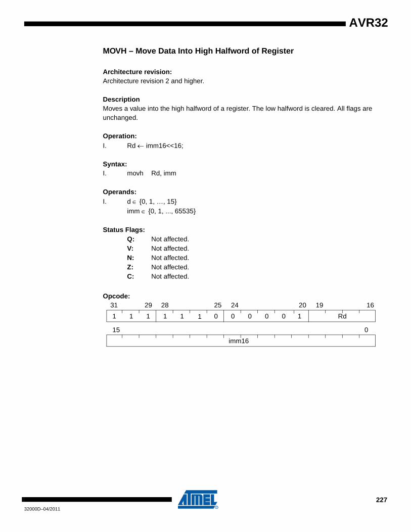
AVR32
MOVH – Move Data Into High Halfword of Register
Architecture revision: Architecture revision 2 and higher.
DescriptionMoves a value into the high halfword of a register. The low halfword is cleared. All flags are unchanged.
Operation:I. Rd ← imm16<<16;
Syntax:I. movh Rd, imm
Operands:I. d ∈ {0, 1, …, 15}
imm ∈ {0, 1, ..., 65535}
Status Flags:Q: Not affected.V: Not affected.N: Not affected.Z: Not affected.C: Not affected.
Opcode:
1 1 1 1 1 0 0 0 0 0 Rd
31 29 28 25 24 20 19 16
imm16
15 0
1 1
22732000D–04/2011

MTDR – Move to Debug Register
Architecture revision:Architecture revision1 and higher.
DescriptionThe instruction copies the value in the specified register to the specified debug register. Note that special timing concerns must be considered when operating on the system registers, see the Pipeline Chapter for details.
Operation:I. DebugRegister[DebugRegisterAddress << 2] ← Rs;
Syntax:I. mtdr DebugRegisterAddress, Rs
Operands:I. DebugRegisterAddress ∈ {0, 4, 8, ..., 1020}
Status Flags:Q: Not affected.V: Not affected.N: Not affected.Z: Not affected.C: Not affected.
Opcode:
Note: The debug registers are implementation defined, and updates of these registers are handled in an implementation specific way.
This instruction can only be executed in a privileged mode. Execution from any other mode will trigger a Privilege Violation exception.
1 1 1 0 0 1 1 1 1 0 1 1 Rs
31 20 19 16
0 0 0 0 0 0 0 0 Debug Register Ad-
15 8 7 0
22832000D–04/2011
AVR32

AVR32
MTSR – Move to System Register
Architecture revision:Architecture revision1 and higher.
DescriptionThe instruction copies the value in the specified register to the specified system register. Note that special timing concerns must be considered when operating on the system registers, see the Implementation Manual for details.
Operation:I. SystemRegister[SystemRegisterAddress << 2] ← Rs;
Syntax:I. mtsr SystemRegisterAddress, Rs
Operands:I. SystemRegisterAddress ∈ {0, 4, 8, ..., 1020}
Status Flags:Q: Not affected.V: Not affected.N: Not affected.Z: Not affected.C: Not affected.
Opcode:
Note: Some system registers are implementation defined. If writing a system register that does notexist, or to a register that is read only, the instruction is executed but no registers are updated.
With the exception of accessing the JECR and JOSP system registers, this instruction can onlybe executed in a privileged mode. Execution from any other mode will trigger a Privilege Viola-tion exception. JECR and JOSP can be accessed from all modes with this instruction.
The instruction mtsr JOSP, Rx must be used with care. The programmer must ensure that nochange of flow instruction nor an INCJOSP instruction follows mtsr JOSP, Rx within a number ofinstructions. This number of cycles is implementation defined. It should also be noted, that this istrue even if the instructions are not to be executed. For instance the sequence
mtsr JOSP, Rxretjincjosp
1 1 1 0 0 0 1 1 1 0 1 1 Rs
31 20 19 16
0 0 0 0 0 0 0 0 System Register Ad-
15 8 7 0
22932000D–04/2011

will execute with an incorrect result. In practice this warning will only affect programmers writing their own Java Virtual Machine based on the AVR32 Java Extension module.
23032000D–04/2011
AVR32
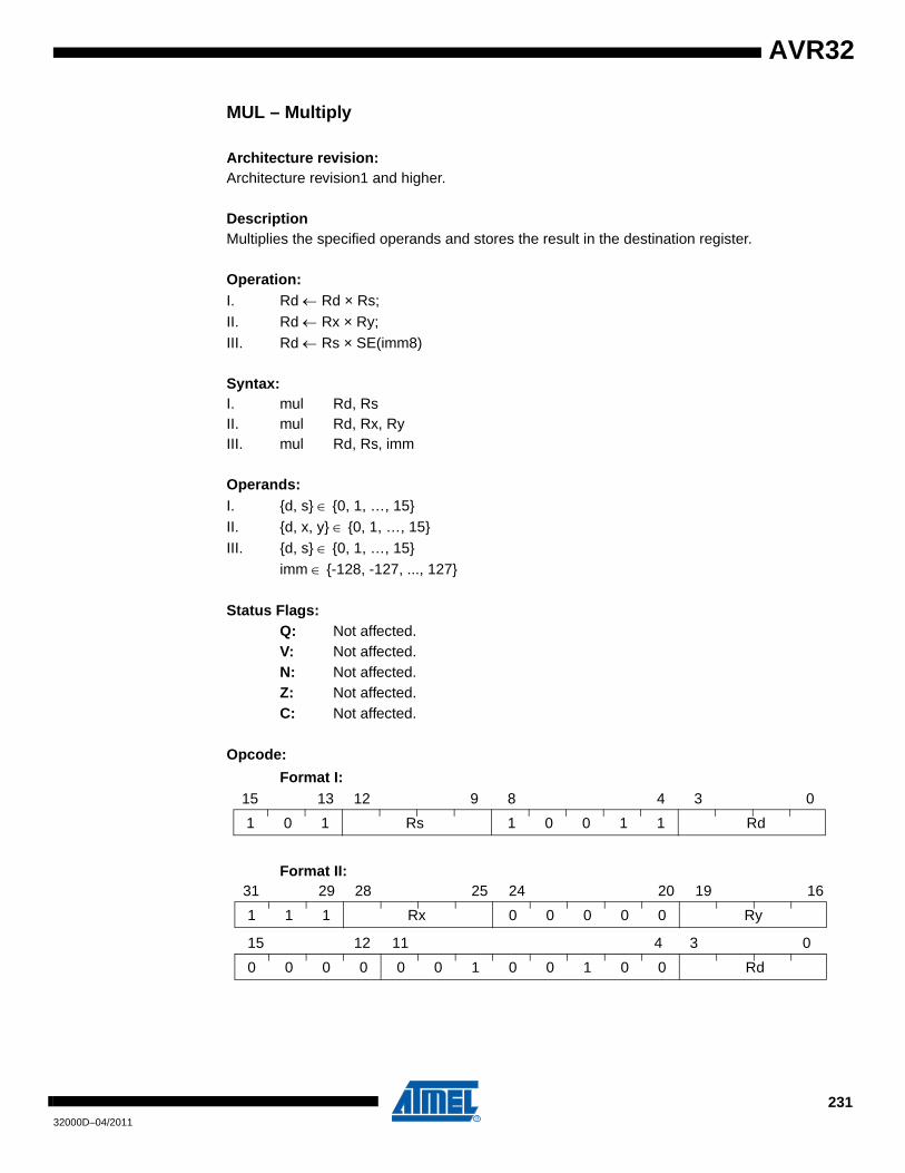
AVR32
MUL – Multiply
Architecture revision:Architecture revision1 and higher.
DescriptionMultiplies the specified operands and stores the result in the destination register.
Operation:I. Rd ← Rd × Rs;II. Rd ← Rx × Ry;III. Rd ← Rs × SE(imm8)
Syntax:I. mul Rd, RsII. mul Rd, Rx, RyIII. mul Rd, Rs, imm
Operands:I. {d, s} ∈ {0, 1, …, 15}II. {d, x, y} ∈ {0, 1, …, 15}III. {d, s} ∈ {0, 1, …, 15}
imm ∈ {-128, -127, ..., 127}
Status Flags:Q: Not affected.V: Not affected.N: Not affected.Z: Not affected.C: Not affected.
Opcode:
Format I:
Format II:
1 0 1 Rs 1 0 0 1 1 Rd
15 13 12 9 8 4 3 0
1 1 1 Rx 0 0 0 0 0 Ry
31 29 28 25 24 20 19 16
0 0 0 0 0 0 1 0 0 1 0 0 Rd
15 12 11 4 3 0
23132000D–04/2011

Format III:
1 1 1 Rs 0 0 0 0 0 Rd
31 29 28 25 24 20 19 16
0 0 0 1 0 0 0 0 imm8
15 12 11 8 7 0
23232000D–04/2011
AVR32
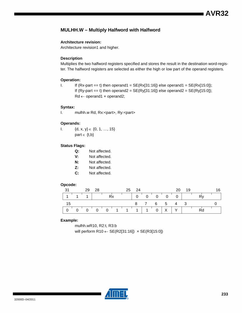
AVR32
MULHH.W – Multiply Halfword with Halfword
Architecture revision:Architecture revision1 and higher.
DescriptionMultiplies the two halfword registers specified and stores the result in the destination word-regis-ter. The halfword registers are selected as either the high or low part of the operand registers.
Operation:I. If (Rx-part == t) then operand1 = SE(Rx[31:16]) else operand1 = SE(Rx[15:0]);
If (Ry-part == t) then operand2 = SE(Ry[31:16]) else operand2 = SE(Ry[15:0]);Rd ← operand1 × operand2;
Syntax:I. mulhh.w Rd, Rx:<part>, Ry:<part>
Operands:I. {d, x, y} ∈ {0, 1, …, 15}
part ∈ {t,b}
Status Flags:Q: Not affected.V: Not affected.N: Not affected.Z: Not affected.C: Not affected.
Opcode:
Example:mulhh.wR10, R2:t, R3:bwill perform R10 ← SE(R2[31:16]) × SE(R3[15:0])
1 1 1 Rx 0 0 0 0 0 Ry
31 29 28 25 24 20 19 16
0 0 0 0 0 1 1 1 1 0 X Y Rd
15 8 7 6 5 4 3 0
23332000D–04/2011
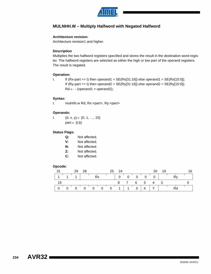
MULNHH.W – Multiply Halfword with Negated Halfword
Architecture revision:Architecture revision1 and higher.
DescriptionMultiplies the two halfword registers specified and stores the result in the destination word-regis-ter. The halfword registers are selected as either the high or low part of the operand registers. The result is negated.
Operation:I. If (Rx-part == t) then operand1 = SE(Rx[31:16]) else operand1 = SE(Rx[15:0]);
If (Ry-part == t) then operand2 = SE(Ry[31:16]) else operand2 = SE(Ry[15:0]);Rd ← - (operand1 × operand2);
Syntax:I. mulnhh.w Rd, Rx:<part>, Ry:<part>
Operands:I. {d, x, y} ∈ {0, 1, …, 15}
part ∈ {t,b}
Status Flags:Q: Not affected.V: Not affected.N: Not affected.Z: Not affected.C: Not affected.
Opcode:
1 1 1 Rx 0 0 0 0 0 Ry
31 29 28 25 24 20 19 16
0 0 0 0 0 0 0 1 1 0 X Y Rd
15 8 7 6 5 4 3 0
23432000D–04/2011
AVR32
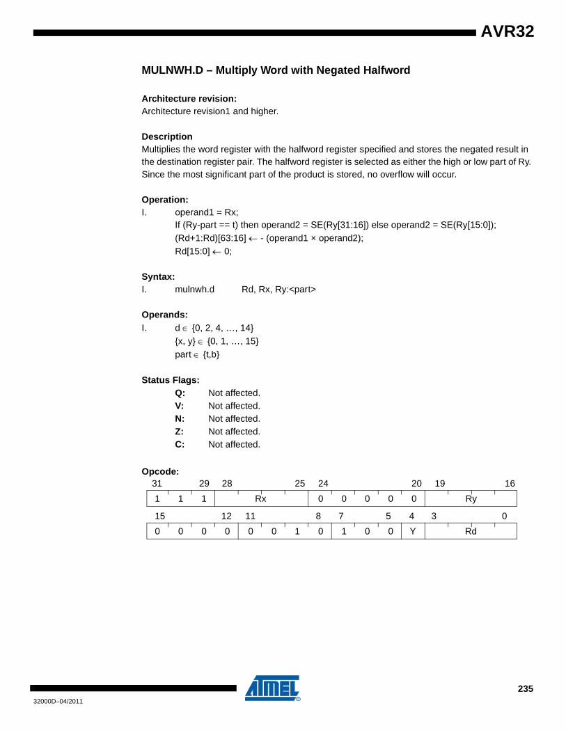
AVR32
MULNWH.D – Multiply Word with Negated Halfword
Architecture revision:Architecture revision1 and higher.
DescriptionMultiplies the word register with the halfword register specified and stores the negated result in the destination register pair. The halfword register is selected as either the high or low part of Ry. Since the most significant part of the product is stored, no overflow will occur.
Operation:I. operand1 = Rx;
If (Ry-part == t) then operand2 = SE(Ry[31:16]) else operand2 = SE(Ry[15:0]);(Rd+1:Rd)[63:16] ← - (operand1 × operand2);Rd[15:0] ← 0;
Syntax:I. mulnwh.d Rd, Rx, Ry:<part>
Operands:I. d ∈ {0, 2, 4, …, 14}
{x, y} ∈ {0, 1, …, 15}part ∈ {t,b}
Status Flags:Q: Not affected.V: Not affected.N: Not affected.Z: Not affected.C: Not affected.
Opcode:
1 1 1 Rx 0 0 0 0 0 Ry
31 29 28 25 24 20 19 16
0 0 0 0 0 0 1 0 1 0 0 Y Rd
15 12 11 8 7 5 4 3 0
23532000D–04/2011

MULS.D – Multiply Signed
Architecture revision:Architecture revision1 and higher.
DescriptionMultiplies the two registers specified and stores the result in the destination registers.
Operation:I. Rd+1:Rd ← Rx × Ry;
Syntax:I. muls.d Rd, Rx, Ry
Operands:I. d ∈ {0, 2, 4, …, 14}
{x, y} ∈ {0, 1, …, 15}
Status FlagsQ: Not affected.V: Not affected.N: Not affected.Z: Not affected.C: Not affected.
Opcode:
1 1 1 Rx 0 0 0 0 0 Ry
31 29 28 25 24 20 19 16
0 0 0 0 0 1 0 0 0 1 0 0 Rd
15 12 11 4 3 0
23632000D–04/2011
AVR32
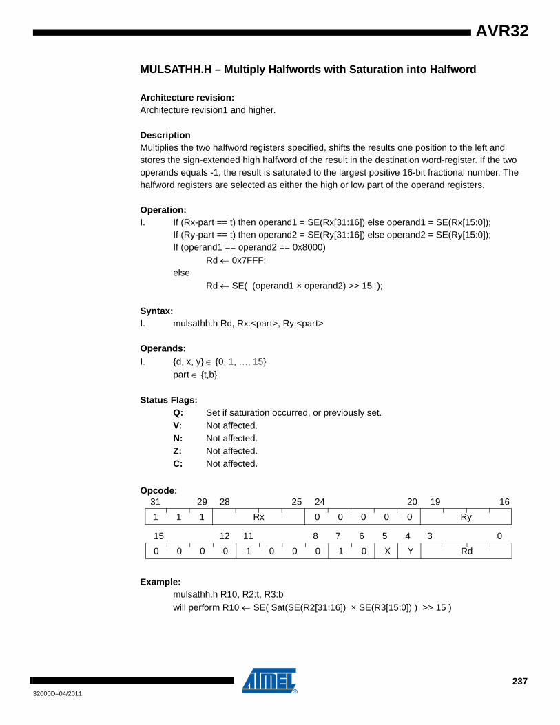
AVR32
MULSATHH.H – Multiply Halfwords with Saturation into Halfword
Architecture revision:Architecture revision1 and higher.
DescriptionMultiplies the two halfword registers specified, shifts the results one position to the left and stores the sign-extended high halfword of the result in the destination word-register. If the two operands equals -1, the result is saturated to the largest positive 16-bit fractional number. The halfword registers are selected as either the high or low part of the operand registers.
Operation:I. If (Rx-part == t) then operand1 = SE(Rx[31:16]) else operand1 = SE(Rx[15:0]);
If (Ry-part == t) then operand2 = SE(Ry[31:16]) else operand2 = SE(Ry[15:0]);If (operand1 == operand2 == 0x8000)
Rd ← 0x7FFF;else
Rd ← SE( (operand1 × operand2) >> 15 );
Syntax:I. mulsathh.h Rd, Rx:<part>, Ry:<part>
Operands:I. {d, x, y} ∈ {0, 1, …, 15}
part ∈ {t,b}
Status Flags:Q: Set if saturation occurred, or previously set.V: Not affected.N: Not affected.Z: Not affected.C: Not affected.
Opcode:
Example:mulsathh.h R10, R2:t, R3:bwill perform R10 ← SE( Sat(SE(R2[31:16]) × SE(R3[15:0]) ) >> 15 )
1 1 1 Rx 0 0 0 0 0 Ry
31 29 28 25 24 20 19 16
0 0 0 0 1 0 0 0 1 0 X Y Rd
15 12 11 8 7 6 5 4 3 0
23732000D–04/2011

MULSATHH.W – Multiply Halfwords with Saturation into Word
Architecture revision:Architecture revision1 and higher.
DescriptionMultiplies the two halfword registers specified, shifts the results one position to the left and stores the result in the destination word-register. If the two operands equals -1, the result is sat-urated to the largest positive 32-bit fractional number. The halfword registers are selected as either the high or low part of the operand registers.
Operation:I. If (Rx-part == t) then operand1 = SE(Rx[31:16]) else operand1 = SE(Rx[15:0]);
If (Ry-part == t) then operand2 = SE(Ry[31:16]) else operand2 = SE(Ry[15:0]);If (operand1 == operand2 == 0x8000)
Rd ← 0x7FFF_FFFF;else
Rd ← (operand1 × operand2) << 1;
Syntax:I. mulsathh.w Rd, Rx:<part>, Ry:<part>
Operands:I. {d, x, y} ∈ {0, 1, …, 15}
part ∈ {t,b}
Status Flags:Q: Set if saturation occurred, or previously set.V: Not affected.N: Not affected.Z: Not affected.C: Not affected.
Opcode:
Example:mulsathh.w R10, R2:t, R3:bwill perform R10 ← Sat( (SE(R2[31:16]) × SE(R3[15:0] )) << 1)
1 1 1 Rx 0 0 0 0 0 Ry
31 29 28 25 24 20 19 16
0 0 0 0 1 0 0 1 1 0 X Y Rd
15 12 11 8 7 6 5 4 3 0
23832000D–04/2011
AVR32
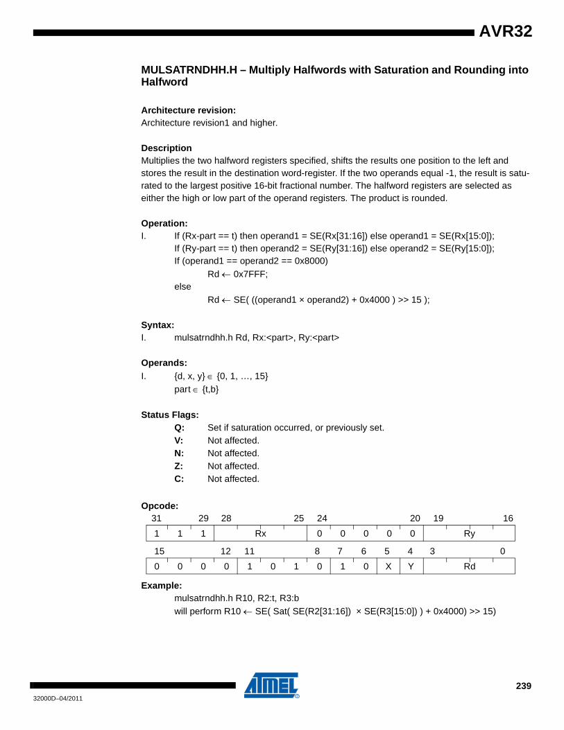
AVR32
MULSATRNDHH.H – Multiply Halfwords with Saturation and Rounding into Halfword
Architecture revision:Architecture revision1 and higher.
DescriptionMultiplies the two halfword registers specified, shifts the results one position to the left and stores the result in the destination word-register. If the two operands equal -1, the result is satu-rated to the largest positive 16-bit fractional number. The halfword registers are selected as either the high or low part of the operand registers. The product is rounded.
Operation:I. If (Rx-part == t) then operand1 = SE(Rx[31:16]) else operand1 = SE(Rx[15:0]);
If (Ry-part == t) then operand2 = SE(Ry[31:16]) else operand2 = SE(Ry[15:0]);If (operand1 == operand2 == 0x8000)
Rd ← 0x7FFF;else
Rd ← SE( ((operand1 × operand2) + 0x4000 ) >> 15 );
Syntax:I. mulsatrndhh.h Rd, Rx:<part>, Ry:<part>
Operands:I. {d, x, y} ∈ {0, 1, …, 15}
part ∈ {t,b}
Status Flags:Q: Set if saturation occurred, or previously set.V: Not affected.N: Not affected.Z: Not affected.C: Not affected.
Opcode:
Example:mulsatrndhh.h R10, R2:t, R3:bwill perform R10 ← SE( Sat( SE(R2[31:16]) × SE(R3[15:0]) ) + 0x4000) >> 15)
1 1 1 Rx 0 0 0 0 0 Ry
31 29 28 25 24 20 19 16
0 0 0 0 1 0 1 0 1 0 X Y Rd
15 12 11 8 7 6 5 4 3 0
23932000D–04/2011
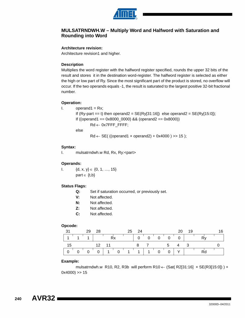
MULSATRNDWH.W – Multiply Word and Halfword with Saturation and Rounding into Word
Architecture revision:Architecture revision1 and higher.
DescriptionMultiplies the word register with the halfword register specified, rounds the upper 32 bits of the result and stores it in the destination word-register. The halfword register is selected as either the high or low part of Ry. Since the most significant part of the product is stored, no overflow will occur. If the two operands equals -1, the result is saturated to the largest positive 32-bit fractional number.
Operation:I. operand1 = Rx;
If (Ry-part == t) then operand2 = SE(Ry[31:16]) else operand2 = SE(Ry[15:0]);If ((operand1 == 0x8000_0000) && (operand2 == 0x8000))
Rd ← 0x7FFF_FFFF;else
Rd ← SE( ((operand1 × operand2) + 0x4000 ) >> 15 );
Syntax:I. mulsatrndwh.w Rd, Rx, Ry:<part>
Operands:I. {d, x, y} ∈ {0, 1, …, 15}
part ∈ {t,b}
Status Flags:Q: Set if saturation occurred, or previously set.V: Not affected.N: Not affected.Z: Not affected.C: Not affected.
Opcode:
Example:mulsatrndwh.w R10, R2, R3b will perform R10 ← (Sat( R2[31:16] × SE(R3[15:0]) ) +
0x4000) >> 15
1 1 1 Rx 0 0 0 0 0 Ry
31 29 28 25 24 20 19 16
0 0 0 0 1 0 1 1 1 0 0 Y Rd
15 12 11 8 7 5 4 3 0
24032000D–04/2011
AVR32

AVR32
MULSATWH.W – Multiply Word and Halfword with Saturation into Word
Architecture revision:Architecture revision1 and higher.
DescriptionMultiplies the word register with the halfword register specified and stores the upper 32 bits of the result in the destination word-register. The halfword register is selected as either the high or low part of Ry. Since the most significant part of the product is stored, no overflow will occur. If the two operands equal -1, the result is saturated to the largest positive 32-bit fractional number.
Operation:I. operand1 = Rx;
If (Ry-part == t) then operand2 = SE(Ry[31:16]) else operand2 = SE(Ry[15:0]);If ((operand1 == 0x8000_0000) && (operand2 == 0x8000))
Rd ← 0x7FFF_FFFF;else
Rd ← (operand1 × operand2) >> 15;
Syntax:I. mulsatwh.w Rd, Rx, Ry:<part>
Operands:I. {d, x, y} ∈ {0, 1, …, 15}
part ∈ {t,b}
Status Flags:Q: Set if saturation occurred, or previously set.V: Not affected.N: Not affected.Z: Not affected.C: Not affected.
Opcode:
Example:mulsatwh.wR10, R2, R3:bwill perform R10 ← Sat( R2 × SE(R3[15:0])) >> 15
1 1 1 Rx 0 0 0 0 0 Ry
31 29 28 25 24 20 19 16
0 0 0 0 1 1 1 0 1 0 0 Y Rd
15 12 11 8 7 5 4 3 0
24132000D–04/2011

MULU.D – Multiply Unsigned
Architecture revision:Architecture revision1 and higher.
DescriptionMultiplies the two registers specified and stores the result in the destination registers.
Operation:I. Rd+1:Rd ← Rx × Ry;
Syntax:I. mulu.d Rd, Rx, Ry
Operands:I. d ∈ {0, 2, 4, …, 14}
{x, y} ∈ {0, 1, …, 15}
Status FlagsQ: Not affected.V: Not affected.N: Not affected.Z: Not affected.C: Not affected.
Opcode:
1 1 1 Rx 0 0 0 0 0 Rd
31 29 28 25 24 20 19 16
0 0 0 0 0 1 1 0 0 1 0 0 Rd
15 12 11 4 3 0
24232000D–04/2011
AVR32
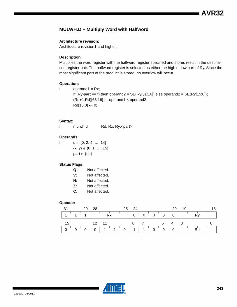
AVR32
MULWH.D – Multiply Word with Halfword
Architecture revision:Architecture revision1 and higher.
DescriptionMultiplies the word register with the halfword register specified and stores result in the destina-tion register pair. The halfword register is selected as either the high or low part of Ry. Since the most significant part of the product is stored, no overflow will occur.
Operation:I. operand1 = Rx;
If (Ry-part == t) then operand2 = SE(Ry[31:16]) else operand2 = SE(Ry[15:0]);(Rd+1:Rd)[63:16] ← operand1 × operand2;Rd[15:0] ← 0;
Syntax:I. mulwh.d Rd, Rx, Ry:<part>
Operands:I. d ∈ {0, 2, 4, …, 14}
{x, y} ∈ {0, 1, …, 15}part ∈ {t,b}
Status Flags:Q: Not affected.V: Not affected.N: Not affected.Z: Not affected.C: Not affected.
Opcode:
1 1 1 Rx 0 0 0 0 0 Ry
31 29 28 25 24 20 19 16
0 0 0 0 1 1 0 1 1 0 0 Y Rd
15 12 11 8 7 5 4 3 0
24332000D–04/2011
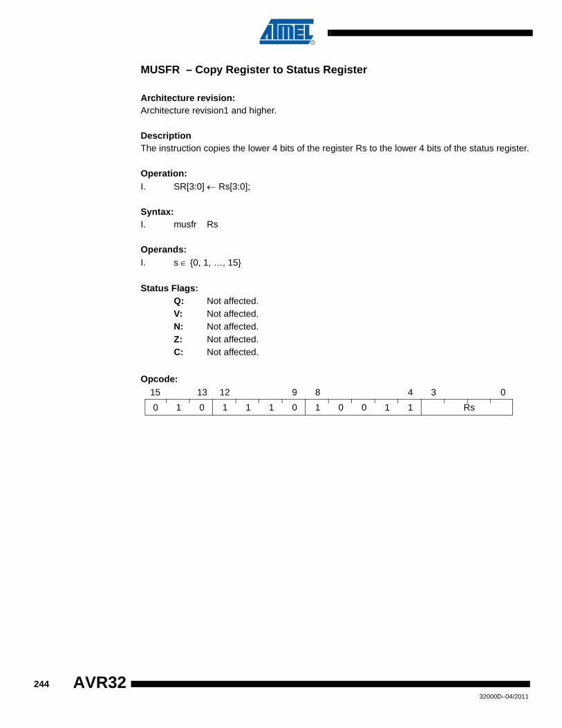
MUSFR – Copy Register to Status Register
Architecture revision:Architecture revision1 and higher.
DescriptionThe instruction copies the lower 4 bits of the register Rs to the lower 4 bits of the status register.
Operation:I. SR[3:0] ← Rs[3:0];
Syntax:I. musfr Rs
Operands:I. s ∈ {0, 1, …, 15}
Status Flags:Q: Not affected.V: Not affected.N: Not affected.Z: Not affected.C: Not affected.
Opcode:
0 1 0 1 1 1 0 1 0 0 1 1 Rs
15 13 12 9 8 4 3 0
24432000D–04/2011
AVR32
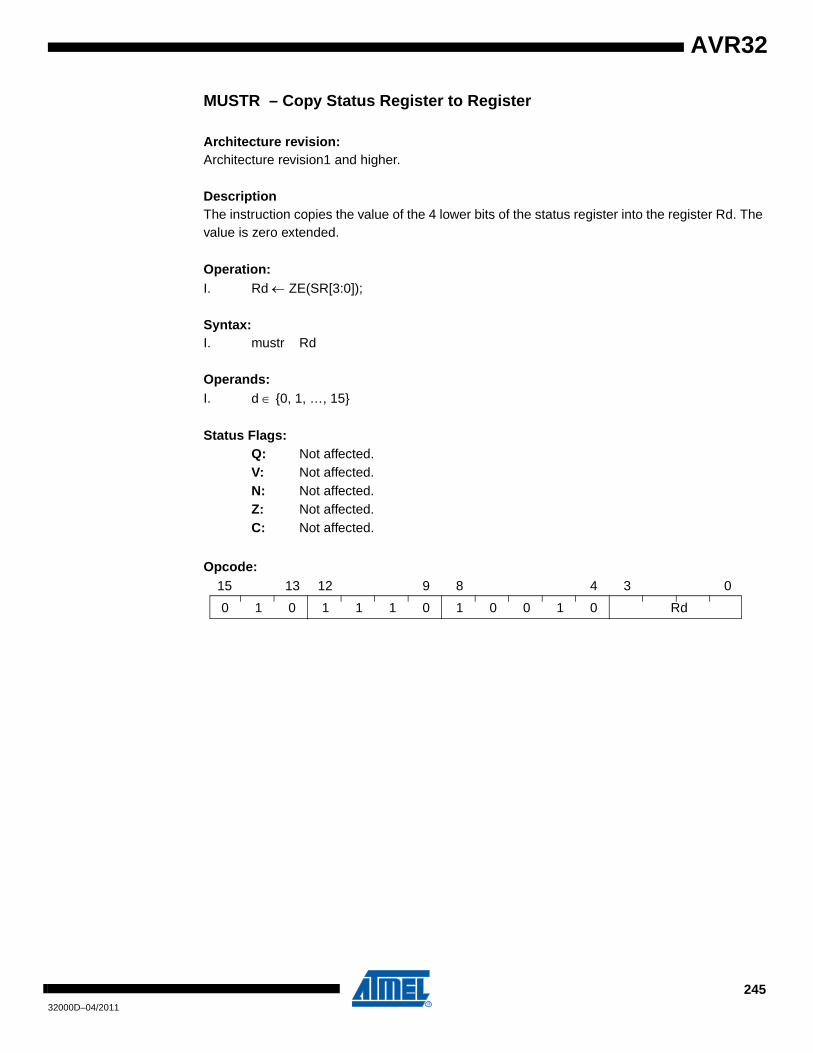
AVR32
MUSTR – Copy Status Register to Register
Architecture revision:Architecture revision1 and higher.
DescriptionThe instruction copies the value of the 4 lower bits of the status register into the register Rd. The value is zero extended.
Operation:I. Rd ← ZE(SR[3:0]);
Syntax:I. mustr Rd
Operands:I. d ∈ {0, 1, …, 15}
Status Flags:Q: Not affected.V: Not affected.N: Not affected.Z: Not affected.C: Not affected.
Opcode:
0 1 0 1 1 1 0 1 0 0 1 0 Rd
15 13 12 9 8 4 3 0
24532000D–04/2011

MVCR.{D,W} – Move Coprocessor Register to Register file
Architecture revision:Architecture revision1 and higher.
DescriptionAddresses a coprocessor and moves the specified registers into the register file.
Operation:I. (Rd+1:Rd) ← CP#(CRs+1:CRs);II. Rd ← CP#(CRs);
Syntax:I. mvcr.d CP#, Rd, CRsII. mvcr.w CP#, Rd, CRs
Operands:I. # ∈ {0, 1, …, 7}
{d, s} ∈ {0, 2, 4, …, 14}II. # ∈ {0, 1, …, 7}
{d, s} ∈ {0, 1, …, 15}
Status Flags:Q: Not affectedV: Not affectedN: Not affectedZ: Not affectedC: Not affected
Opcode:
Format I:
Format II:
Example:mvcr.d CP2, R0, CR2
1 1 1 0 1 1 1 1 0 1 0 Rd 0
31 29 28 25 24 20 19 17 16
CP# 0 CRs 0 0 0 0 1 0 0 0 0
15 13 12 11 9 8 7 0
1
1 1 1 0 1 1 1 1 0 1 0 Rd
31 29 28 25 24 20 19 16
CP# 0 CRs 0 0 0 0 0 0 0
15 13 12 11 8 7 0
1
0
24632000D–04/2011
AVR32

AVR32
MVRC.{D,W} – Move Register file Register to Coprocessor Register
Architecture revision:Architecture revision1 and higher.
DescriptionMoves the specified register into the addressed coprocessor.
Operation:I. CP#(CRd+1:CRd) ← Rs+1:Rs;II. CP#(CRd) ← Rs;
Syntax:I. mvrc.d CP#, CRd, RsII. mvrc.w CP#, CRd, Rs
Operands:I. # ∈ {0, 1, …, 7}
{d, s} ∈ {0, 2, 4, …, 14}I. # ∈ {0, 1, …, 7}
{d, s} ∈ {0, 1, …, 15}
Status Flags:Q: Not affectedV: Not affectedN: Not affectedZ: Not affectedC: Not affected
Opcode:
Format I:
Format II:
Example:mvrc.d CP2, CR0, R2
1 1 1 0 1 1 1 1 0 1 0 Rs 0
31 29 28 25 24 20 19 17 16
CP# 0 CRd 0 0 0 1 1 0 0 0 0
15 13 12 11 9 8 7 0
1
1 1 1 0 1 1 1 1 0 1 0 Rs
31 29 28 25 24 20 19 16
CP# 0 CRd 0 0 1 0 0 0 0
15 13 12 11 8 7 0
1
0
24732000D–04/2011

NEG – Two’s Complement
Architecture revision:Architecture revision1 and higher.
DescriptionPerform a two’s complement of specified register.
Operation:I. Rd ← 0 -Rd;
Syntax:I. neg Rd
Operands:I. d ∈ {0, 1, …, 15}
Status Flags:Q: Not affectedV: V ← Rd[31] ∧ RES[31]N: N ← RES[31] Z: Z ← (RES[31:0] == 0)C: C ← Rd[31] ∨ RES[31]
Opcode:
0 1 0 1 1 1 0 0 0 0 1 1 Rd
15 13 12 9 8 4 3 0
24832000D–04/2011
AVR32

AVR32
NOP – No Operation
Architecture revision:Architecture revision1 and higher.
DescriptionSpecial instructions for "no operation" that does not create data depencencies in the pipeline
Operation:I. none
Syntax:I. nop
Operands:I. none
Status Flags:Q: Not affectedV: Not affectedN: Not affected Z: Not affectedC: Not affected
Opcode:
1 1 0 1 0 1 1 1 0 0 0 0 0 0 1 1
15 9 8 4 3 0
24932000D–04/2011

OR – Logical OR with optional logical shift
Architecture revision:Architecture revision1 and higher.
DescriptionPerforms a bitwise logical OR between the specified registers and stores the result in the desti-nation register.
Operation:I. Rd ← Rd ∨ Rs;II. Rd ← Rx ∨ (Ry << sa5);III. Rd ← Rx ∨ (Ry >> sa5);
Syntax:I. or Rd, RsII. or Rd, Rx, Ry << saIII. or Rd, Rx, Ry >> sa
Operands:I. {d, s} ∈ {0, 1, …, 15}II, III. {d, x, y} ∈ {0, 1, …, 15}
sa ∈ {0, 1, …, 31}
Status Flags:Q: Not affected.V: Not affected.N: N ← RES[31]Z: Z ← (RES[31:0] == 0)C: Not affected.
Opcode:
Format I:
Format II:
0 0 0 Rs 0 0 1 0 0 Rd
15 13 12 9 8 4 3 0
1 1 1 Rx 1 1 1 1 0 Ry
31 29 28 25 24 20 19 16
0 0 0 1 0 0 0 sa5 Rd
15 9 8 4 3 0
25032000D–04/2011
AVR32
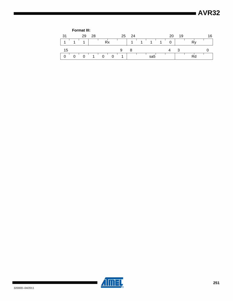
AVR32
Format III:
1 1 1 Rx 1 1 1 1 0 Ry
31 29 28 25 24 20 19 16
0 0 0 1 0 0 1 sa5 Rd
15 9 8 4 3 0
25132000D–04/2011

OR{cond4} – Conditional logical OR
Architecture revision:Architecture revision 2 and higher.
DescriptionPerforms a bitwise logical OR between the specified registers and stores the result in the desti-nation register.
Operation:I. if ( cond4)
Rd ← Rx ∨ Ry;
Syntax:I. or{cond4} Rd, Rx, Ry
Operands:I. {d, x, y} ∈ {0, 1, …, 15}
cond4 ∈ {eq, ne, cc/hs, cs/lo, ge, lt, mi, pl, ls, gt, le, hi, vs, vc, qs, al}
Status Flags:Q: Not affected.V: Not affected.N: Not affected.Z: Not affected.C: Not affected.
Opcode:
1 1 1 1 1 1 0 1 Ry
31 29 28 25 24 20 19 16
1 1 1 0 cond4 0 0 1 1 Rd
15 12 11 8 7 0
Rx
25232000D–04/2011
AVR32
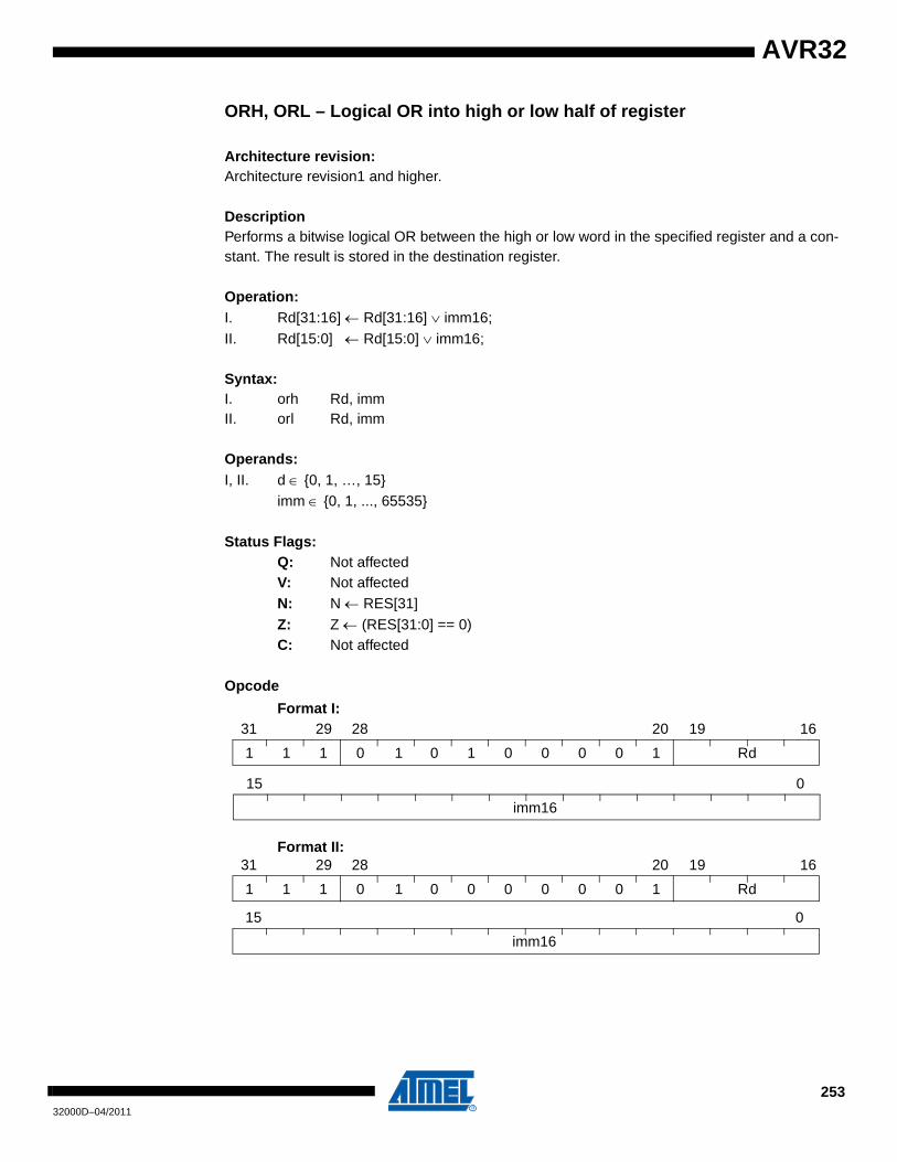
AVR32
ORH, ORL – Logical OR into high or low half of register
Architecture revision:Architecture revision1 and higher.
DescriptionPerforms a bitwise logical OR between the high or low word in the specified register and a con-stant. The result is stored in the destination register.
Operation:I. Rd[31:16] ← Rd[31:16] ∨ imm16;II. Rd[15:0] ← Rd[15:0] ∨ imm16;
Syntax:I. orh Rd, immII. orl Rd, imm
Operands:I, II. d ∈ {0, 1, …, 15}
imm ∈ {0, 1, ..., 65535}
Status Flags:Q: Not affectedV: Not affectedN: N ← RES[31]Z: Z ← (RES[31:0] == 0)C: Not affected
Opcode
Format I:
Format II:
1 1 1 0 0 1 0 0 0 0 1 Rd
31 29 28 20 19 16
imm16
15 0
1
1 1 1 0 0 0 0 0 0 0 1 Rd
31 29 28 20 19 16
imm16
15 0
1
25332000D–04/2011
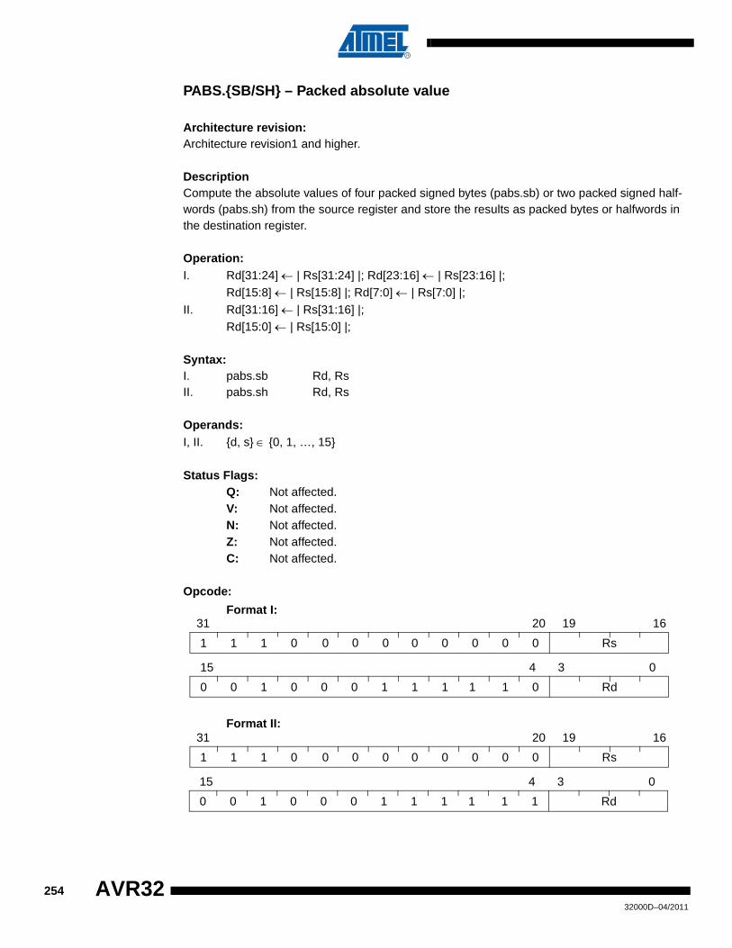
PABS.{SB/SH} – Packed absolute value
Architecture revision:Architecture revision1 and higher.
DescriptionCompute the absolute values of four packed signed bytes (pabs.sb) or two packed signed half-words (pabs.sh) from the source register and store the results as packed bytes or halfwords in the destination register.
Operation:I. Rd[31:24] ← | Rs[31:24] |; Rd[23:16] ← | Rs[23:16] |;
Rd[15:8] ← | Rs[15:8] |; Rd[7:0] ← | Rs[7:0] |;II. Rd[31:16] ← | Rs[31:16] |;
Rd[15:0] ← | Rs[15:0] |;
Syntax:I. pabs.sb Rd, RsII. pabs.sh Rd, Rs
Operands:I, II. {d, s} ∈ {0, 1, …, 15}
Status Flags:Q: Not affected.V: Not affected.N: Not affected.Z: Not affected.C: Not affected.
Opcode:
Format I:
Format II:
1 1 1 0 0 0 0 0 0 Rs
31 20 19 16
0 0 1 0 0 0 1 1 1 1 1 0 Rd
15 4 3 0
0 0 0
1 1 1 0 0 0 0 0 0 Rs
31 20 19 16
0 0 1 0 0 0 1 1 1 1 1 1 Rd
15 4 3 0
0 0 0
25432000D–04/2011
AVR32

AVR32
PACKSH.{UB/SB} – Pack Signed Halfwords to Bytes
Architecture revision:Architecture revision1 and higher.
DescriptionPack the four signed halfwords located in the two source registers into four bytes in the destina-tion register. Each of the signed halfwords are saturated to unsigned (packsh.ub) or signed bytes (packsh.sb).
Operation:I. Rd[31:24] ← SATSU(Rx[31:16], 8); Rd[23:16] ← SATSU(Rx[15:0], 8);
Rd[15:8] ← SATSU(Ry[31:16], 8); Rd[7:0] ← SATSU(Ry[15:0], 8);II. Rd[31:24] ← SATS(Rx[31:16], 8); Rd[23:16] ← SATS(Rx[15:0], 8);
Rd[15:8] ← SATS(Ry[31:16], 8); Rd[7:0] ← SATS(Ry[15:0], 8);
Syntax:I. packsh.ub Rd, Rx, RyII. packsh.sb Rd, Rx, Ry
Operands:I, II. {d, x, y} ∈ {0, 1, …, 15}
Status Flags:Q: Flag set if saturation occured in one or more of the partial operations.V: Not affected.N: Not affected.Z: Not affected.C: Not affected.
Opcode:
Format I:
Format II:
1 1 1 0 0 0 0 0 Ry
31 29 28 25 24 20 19 16
0 0 1 0 0 1 0 0 1 1 0 0 Rd
15 4 3 0
Rx
1 1 1 0 0 0 0 0 Ry
31 29 28 25 24 20 19 16
0 0 1 0 0 1 0 0 1 1 0 1 Rd
15 4 3 0
Rx
25532000D–04/2011

25632000D–04/2011
AVR32
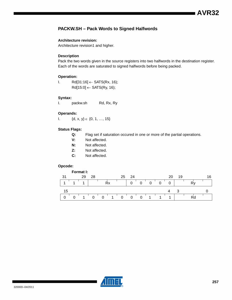
AVR32
PACKW.SH – Pack Words to Signed Halfwords
Architecture revision:Architecture revision1 and higher.
DescriptionPack the two words given in the source registers into two halfwords in the destination register. Each of the words are saturated to signed halfwords before being packed.
Operation:I. Rd[31:16] ← SATS(Rx, 16);
Rd[15:0] ← SATS(Ry, 16);
Syntax:I. packw.sh Rd, Rx, Ry
Operands:I. {d, x, y} ∈ {0, 1, …, 15}
Status Flags:Q: Flag set if saturation occured in one or more of the partial operations.V: Not affected.N: Not affected.Z: Not affected.C: Not affected.
Opcode:
Format I:
1 1 1 0 0 0 0 0 Ry
31 29 28 25 24 20 19 16
0 0 1 0 0 1 0 0 0 1 1 1 Rd
15 4 3 0
Rx
25732000D–04/2011

PADD.{B/H} – Packed Addition
Architecture revision:Architecture revision1 and higher.
DescriptionPerform addition of four pairs of packed bytes (padd.b) or two pairs of halfwords (padd.h). Upon overflow any additional bits are discarded and the result is wrapped around.
Operation:I. Rd[31:24] ← Rx[31:24] + Ry[31:24]; Rd[23:16] ← Rx[23:16] + Ry[23:16];
Rd[15:8] ← Rx[15:8] + Ry[15:8]; Rd[7:0] ← Rx[7:0] + Ry[7:0];II. Rd[31:16] ← Rx[31:16] + Ry[31:16];
Rd[15:0] ← Rx[15:0] + Ry[15:0];
Syntax:I. padd.b Rd, Rx, RyII. padd.h Rd, Rx, Ry
Operands:I, II. {d, x, y} ∈ {0, 1, …, 15}
Status Flags:Q: Not affected.V: Not affected.N: Not affected.Z: Not affected.C: Not affected.
Opcode:
Format I:
Format II:
1 1 1 0 0 0 0 0 Ry
31 29 28 25 24 20 19 16
0 0 1 0 0 0 1 1 0 0 0 0 Rd
15 4 3 0
Rx
1 1 1 0 0 0 0 0 Ry
31 29 28 25 24 20 19 16
0 0 1 0 0 0 0 0 0 0 0 0 Rd
15 4 3 0
Rx
25832000D–04/2011
AVR32
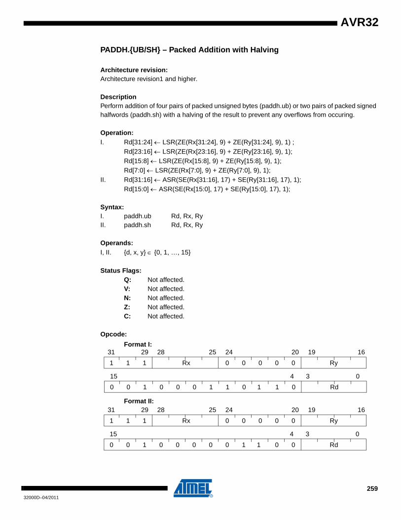
AVR32
PADDH.{UB/SH} – Packed Addition with Halving
Architecture revision:Architecture revision1 and higher.
DescriptionPerform addition of four pairs of packed unsigned bytes (paddh.ub) or two pairs of packed signed halfwords (paddh.sh) with a halving of the result to prevent any overflows from occuring.
Operation:I. Rd[31:24] ← LSR(ZE(Rx[31:24], 9) + ZE(Ry[31:24], 9), 1) ;
Rd[23:16] ← LSR(ZE(Rx[23:16], 9) + ZE(Ry[23:16], 9), 1);Rd[15:8] ← LSR(ZE(Rx[15:8], 9) + ZE(Ry[15:8], 9), 1);Rd[7:0] ← LSR(ZE(Rx[7:0], 9) + ZE(Ry[7:0], 9), 1);
II. Rd[31:16] ← ASR(SE(Rx[31:16], 17) + SE(Ry[31:16], 17), 1);Rd[15:0] ← ASR(SE(Rx[15:0], 17) + SE(Ry[15:0], 17), 1);
Syntax:I. paddh.ub Rd, Rx, RyII. paddh.sh Rd, Rx, Ry
Operands:I, II. {d, x, y} ∈ {0, 1, …, 15}
Status Flags:Q: Not affected.V: Not affected.N: Not affected.Z: Not affected.C: Not affected.
Opcode:
Format I:
Format II:
1 1 1 0 0 0 0 0 Ry
31 29 28 25 24 20 19 16
0 0 1 0 0 0 1 1 0 1 1 0 Rd
15 4 3 0
Rx
1 1 1 0 0 0 0 0 Ry
31 29 28 25 24 20 19 16
0 0 1 0 0 0 0 0 1 1 0 0 Rd
15 4 3 0
Rx
25932000D–04/2011

PADDS.{UB/SB/UH/SH} – Packed Addition with Saturation
Architecture revision:Architecture revision1 and higher.
DescriptionPerform addition of four pairs of packed bytes or two pairs of halfwords. The result is saturated to either unsigned bytes (padds.ub), signed bytes (padds.sb), unsigned halfwords (padds.uh) or signed halfwords (padds.sh).
Operation:I. Rd[31:24] ← SATU(ZE(Rx[31:24], 9) + ZE(Ry[31:24], 9), 8) ;
Rd[23:16] ← SATU(ZE(Rx[23:16], 9) + ZE(Ry[23:16], 9), 8);Rd[15:8] ← SATU(ZE(Rx[15:8], 9) + ZE(Ry[15:8], 9), 8); Rd[7:0] ← SATU(ZE(Rx[7:0], 9) + ZE(Ry[7:0], 9), 8);
II. Rd[31:24] ← SATS(SE(Rx[31:24], 9) + SE(Ry[31:24], 9), 8); Rd[23:16] ← SATS(SE(Rx[23:16], 9) + SE(Ry[23:16], 9), 8);Rd[15:8] ← SATS(SE(Rx[15:8], 9) + SE(Ry[15:8], 9), 8); Rd[7:0] ← SATS(SE(Rx[7:0], 9) + SE(Ry[7:0], 9), 8);
III. Rd[31:16] ← SATU(ZE(Rx[31:16], 17) + ZE(Ry[31:16], 17), 16);Rd[15:0] ← SATU(ZE(Rx[15:0], 17) + ZE(Ry[15:0], 17), 16);
IV. Rd[31:16] ← SATS(SE(Rx[31:16], 17) + SE(Ry[31:16], 17), 16);Rd[15:0] ← SATS(SE(Rx[15:0], 17) + SE(Ry[15:0], 17), 16);
Syntax:I. padds.ub Rd, Rx, RyII. padds.sb Rd, Rx, RyIII. padds.uh Rd, Rx, RyIV. padds.sh Rd, Rx, Ry
Operands:I, II, III, IV.{d, x, y} ∈ {0, 1, …, 15}
Status Flags:Q: Flag set if saturation occured in one or more of the partial operations.V: Not affected.N: Not affected.Z: Not affected.C: Not affected.
Opcode:
26032000D–04/2011
AVR32
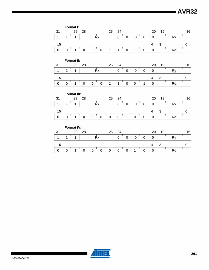
AVR32
Format I:
Format II:
Format III:
Format IV:
1 1 1 0 0 0 0 0 Ry
31 29 28 25 24 20 19 16
0 0 1 0 0 0 1 1 0 1 0 0 Rd
15 4 3 0
Rx
1 1 1 0 0 0 0 0 Ry
31 29 28 25 24 20 19 16
0 0 1 0 0 0 1 1 0 0 1 0 Rd
15 4 3 0
Rx
1 1 1 0 0 0 0 0 Ry
31 29 28 25 24 20 19 16
0 0 1 0 0 0 0 0 1 0 0 0 Rd
15 4 3 0
Rx
1 1 1 0 0 0 0 0 Ry
31 29 28 25 24 20 19 16
0 0 1 0 0 0 0 0 0 1 0 0 Rd
15 4 3 0
Rx
26132000D–04/2011

PADDSUB.H – Packed Halfword Addition and Subtraction
Architecture revision:Architecture revision1 and higher.
DescriptionPerform an addition and subtraction on the same halfword operands which are selected from the source registers. The two halfword results are packed into the destination register without per-forming any saturation.
Operation:
I. If (Rx-part == t) then operand1 = Rx[31:16] else operand1 = Rx[15:0];If (Ry-part == t) then operand2 = Ry[31:16] else operand2 = Ry[15:0];Rd[31:16] ← operand1 + operand2;Rd[15:0] ← operand1 - operand2;
Syntax:I. paddsub.h Rd, Rx:<part>, Ry:<part>
Operands:I. {d, x, y} ∈ {0, 1, …, 15}
part ∈ {t,b}
Status Flags:Q: Not affected.V: Not affected.N: Not affected.Z: Not affected.C: Not affected.
Opcode:
Format I:
1 1 1 0 0 0 0 0 Ry
31 29 28 25 24 20 19 16
0 0 1 0 0 0 0 1 0 0 X Y Rd
15 6 5 4 3 0
Rx
26232000D–04/2011
AVR32

AVR32
PADDSUBH.SH – Packed Halfword Addition and Subtraction with Halving
DescriptionPerform an addition and subtraction on the same signed halfword operands which are selected from the source registers. The halfword results are halved in order to prevent any overflows from occuring
Operation:
I. If (Rx-part == t) then operand1 = Rx[31:16] else operand1 = Rx[15:0];If (Ry-part == t) then operand2 = Ry[31:16] else operand2 = Ry[15:0];Rd[31:16] ← ASR(SE(operand1, 17) + SE(operand2, 17), 1);Rd[15:0] ← ASR(SE(operand1, 17) - SE(operand2, 17), 1);
Syntax:I. paddsubh.sh Rd, Rx:<part>, Ry:<part>
Operands:I. {d, x, y} ∈ {0, 1, …, 15}
part ∈ {t,b}
Status Flags:Q: Not affected.V: Not affected.N: Not affected.Z: Not affected.C: Not affected.
Opcode:
Format I:
1 1 1 0 0 0 0 0 Ry
31 29 28 25 24 20 19 16
0 0 1 0 0 0 1 0 1 0 X Y Rd
15 6 5 4 3 0
Rx
26332000D–04/2011
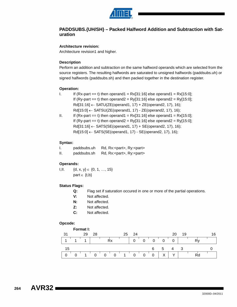
PADDSUBS.{UH/SH} – Packed Halfword Addition and Subtraction with Sat-uration
Architecture revision:Architecture revision1 and higher.
DescriptionPerform an addition and subtraction on the same halfword operands which are selected from the source registers. The resulting halfwords are saturated to unsigned halfwords (paddsubs.uh) or signed halfwords (paddsubs.sh) and then packed together in the destination register.
Operation:I. If (Rx-part == t) then operand1 = Rx[31:16] else operand1 = Rx[15:0];
If (Ry-part == t) then operand2 = Ry[31:16] else operand2 = Ry[15:0];Rd[31:16] ← SATU(ZE(operand1, 17) + ZE(operand2, 17), 16);Rd[15:0] ← SATSU(ZE(operand1, 17) - ZE(operand2, 17), 16);
II. If (Rx-part == t) then operand1 = Rx[31:16] else operand1 = Rx[15:0];If (Ry-part == t) then operand2 = Ry[31:16] else operand2 = Ry[15:0];Rd[31:16] ← SATS(SE(operand1, 17) + SE(operand2, 17), 16);Rd[15:0] ← SATS(SE(operand1, 17) - SE(operand2, 17), 16);
Syntax:I. paddsubs.uh Rd, Rx:<part>, Ry:<part>II. paddsubs.sh Rd, Rx:<part>, Ry:<part>
Operands:I,II. {d, x, y} ∈ {0, 1, …, 15}
part ∈ {t,b}
Status Flags:Q: Flag set if saturation occured in one or more of the partial operations.V: Not affected.N: Not affected.Z: Not affected.C: Not affected.
Opcode:
Format I:
1 1 1 0 0 0 0 0 Ry
31 29 28 25 24 20 19 16
0 0 1 0 0 0 1 0 0 0 X Y Rd
15 6 5 4 3 0
Rx
26432000D–04/2011
AVR32
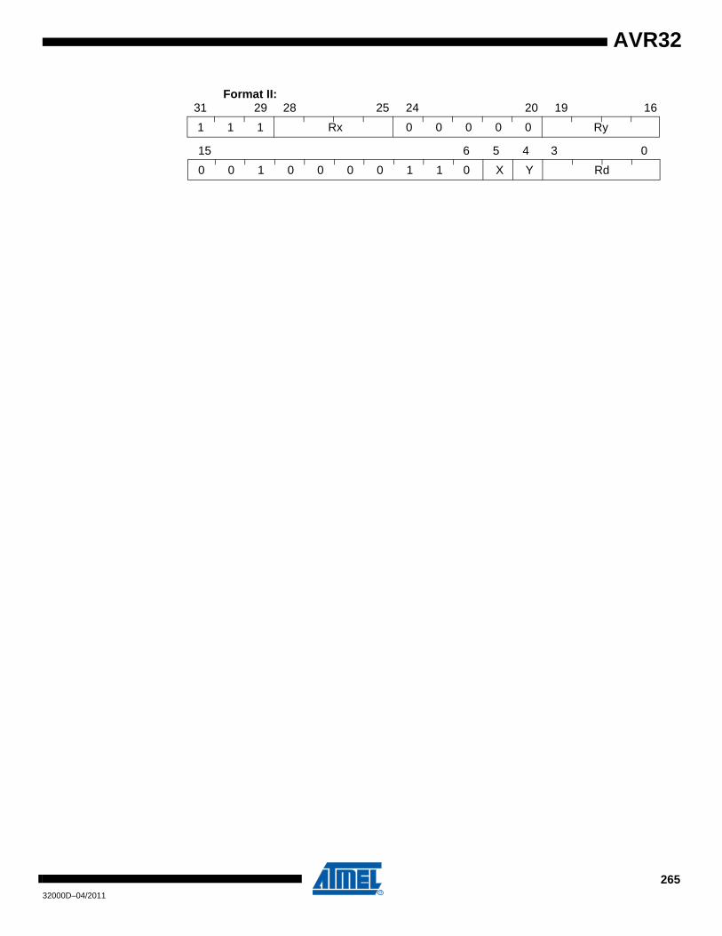
AVR32
Format II:
1 1 1 0 0 0 0 0 Ry
31 29 28 25 24 20 19 16
0 0 1 0 0 0 0 1 1 0 X Y Rd
15 6 5 4 3 0
Rx
26532000D–04/2011

PADDX.H – Packed Halfword Addition with Crossed Operand
Architecture revision:Architecture revision1 and higher.
DescriptionAdd together the top halfword of Rx with the bottom halfword of Ry and the bottom halfword of Rx with the top halfword of Ry. The resulting halfwords are packed together in the destination register without performing any saturation.
Operation:I. Rd[31:16] ← Rx[31:16] + Ry[15:0] ;
Rd[15:0] ← Rx[15:0] + Ry[31:16];
Syntax:I. paddx.h Rd, Rx, Ry
Operands:I. {d, x, y} ∈ {0, 1, …, 15}
Status Flags:Q: Not affected.V: Not affected.N: Not affected.Z: Not affected.C: Not affected.
Opcode:
Format I:
1 1 1 0 0 0 0 0 Ry
31 29 28 25 24 20 19 16
0 0 1 0 0 0 0 0 0 0 1 0 Rd
Rx
15 4 3 0
26632000D–04/2011
AVR32
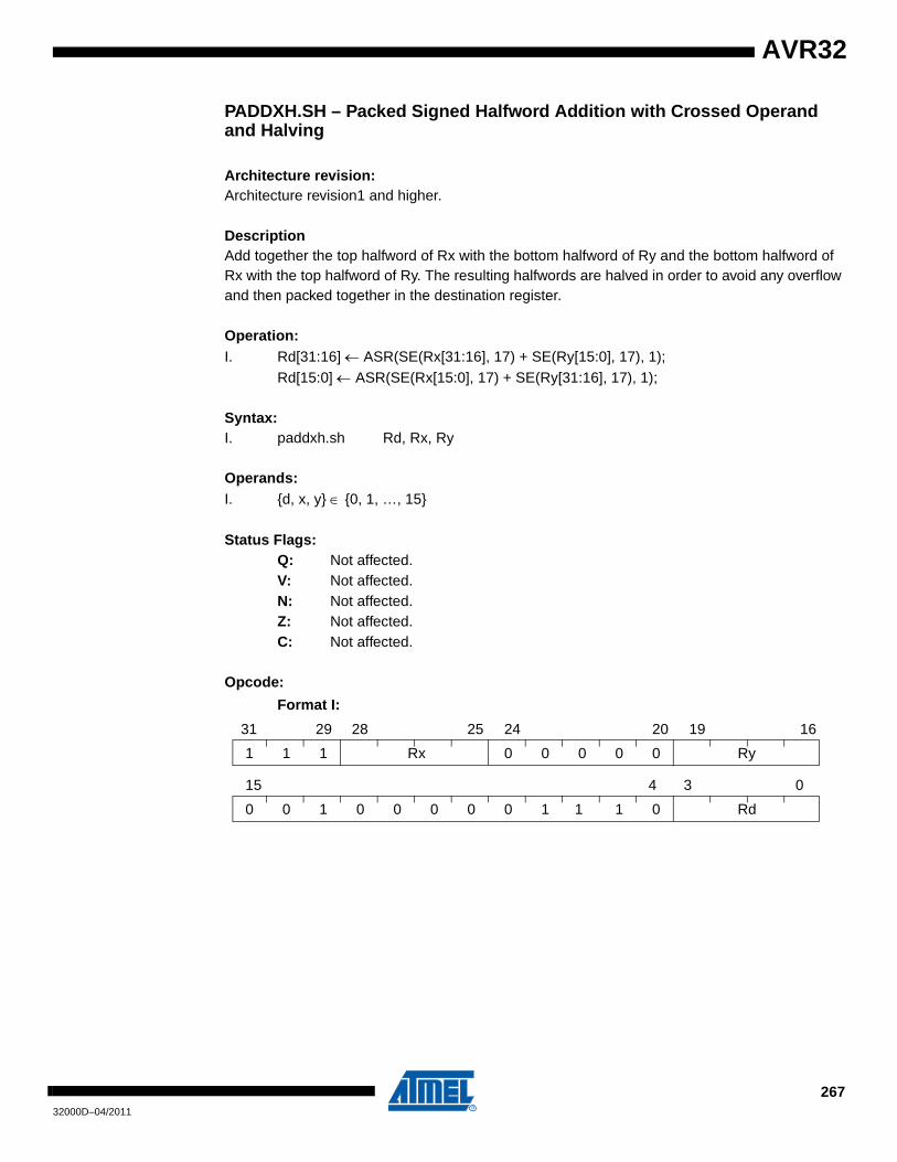
AVR32
PADDXH.SH – Packed Signed Halfword Addition with Crossed Operand and Halving
Architecture revision:Architecture revision1 and higher.
DescriptionAdd together the top halfword of Rx with the bottom halfword of Ry and the bottom halfword of Rx with the top halfword of Ry. The resulting halfwords are halved in order to avoid any overflow and then packed together in the destination register.
Operation:I. Rd[31:16] ← ASR(SE(Rx[31:16], 17) + SE(Ry[15:0], 17), 1);
Rd[15:0] ← ASR(SE(Rx[15:0], 17) + SE(Ry[31:16], 17), 1);
Syntax:I. paddxh.sh Rd, Rx, Ry
Operands:I. {d, x, y} ∈ {0, 1, …, 15}
Status Flags:Q: Not affected.V: Not affected.N: Not affected.Z: Not affected.C: Not affected.
Opcode:
Format I:
1 1 1 0 0 0 0 0 Ry
31 29 28 25 24 20 19 16
0 0 1 0 0 0 0 0 1 1 1 0 Rd
15 4 3 0
Rx
26732000D–04/2011

PADDXS.{UH/SH} – Packed Halfword Addition with Crossed Operand and Saturation
Architecture revision:Architecture revision1 and higher.
DescriptionAdd together the top halfword of Rx with the bottom halfword of Ry and the bottom halfword of Rx with the top halfword of Ry. The resulting halfwords are saturated to unsigned halfwords (paddxh.uh) or signed halfwords (paddxh.sh) and then packed together in the destination regis-ter.
Operation:I. Rd[31:16] ← SATU(ZE(Rx[31:16], 17) + ZE(Ry[15:0], 17), 16) ;
Rd[15:0] ← SATU(ZE(Rx[15:0], 17) + ZE(Ry[31:16], 17), 16);II. Rd[31:16] ← SATS(SE(Rx[31:16], 17) + SE(Ry[15:0], 17), 16) ;
Rd[15:0] ← SATS(SE(Rx[15:0], 17) + SE(Ry[31:16], 17), 16);
Syntax:I. paddxs.uh Rd, Rx, RyII. paddxs.sh Rd, Rx, Ry
Operands:I, II. {d, x, y} ∈ {0, 1, …, 15}
Status Flags:Q: Flag set if saturation occured in one or more of the partial operations.V: Not affected.N: Not affected.Z: Not affected.C: Not affected.
Opcode:
Format I:
Format II:
1 1 1 0 0 0 0 0 Ry
31 29 28 25 24 20 19 16
0 0 1 0 0 0 0 0 1 0 1 0 Rd
15 4 3 0
Rx
1 1 1 0 0 0 0 0 Ry
31 29 28 25 24 20 19 16
0 0 1 0 0 0 0 0 0 1 1 0 Rd
15 4 3 0
Rx
26832000D–04/2011
AVR32

AVR32
PASR.{B/H} – Packed Arithmetic Shift Right
Architecture revision:Architecture revision1 and higher.
DescriptionPerform an arithmetic shift right on each of the packed bytes or halfwords in the source register.
Operation:I. Rd[31:24] ← ASR(Rs[31:24], sa3);
Rd[23:16] ← ASR(Rs[23:16], sa3);Rd[15:8] ← ASR(Rs[15:8], sa3);Rd[7:0] ← ASR(Rs[7:0], sa3);
II. Rd[31:16] ← ASR(Rs[31:16], sa4);Rd[15:0] ← ASR(Rs[15:0], sa4);
Syntax:I. pasr.b Rd, Rs, saII. pasr.h Rd, Rs, sa
Operands:I, II. {d, s} ∈ {0, 1, …, 15}I. sa ∈ {0, 1, …, 7}II. sa ∈ {0, 1, …, 15}
Status Flags:Q: Not affected.V: Not affected.N: Not affected.Z: Not affected.C: Not affected.
Opcode:
Format I:
1 1 1 0 0 0 0 0 0 sa3
31 29 28 25 24 19 18 16
0 0 1 0 0 1 0 0 0 0 0 1 Rd
15 4 3 0
Rs
26932000D–04/2011

Format II:
1 1 1 0 0 0 0 0 sa4
31 29 28 25 24 20 19 16
0 0 1 0 0 1 0 0 0 1 0 0 Rd
15 4 3 0
Rs
27032000D–04/2011
AVR32
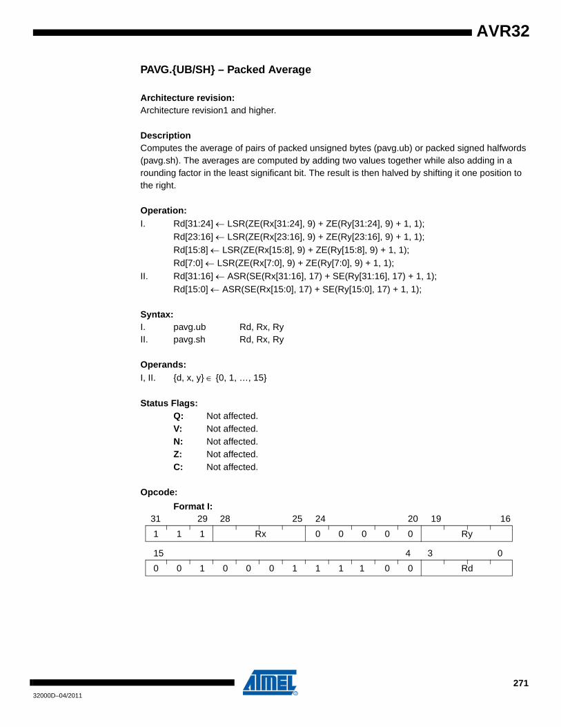
AVR32
PAVG.{UB/SH} – Packed Average
Architecture revision:Architecture revision1 and higher.
DescriptionComputes the average of pairs of packed unsigned bytes (pavg.ub) or packed signed halfwords (pavg.sh). The averages are computed by adding two values together while also adding in a rounding factor in the least significant bit. The result is then halved by shifting it one position to the right.
Operation:I. Rd[31:24] ← LSR(ZE(Rx[31:24], 9) + ZE(Ry[31:24], 9) + 1, 1);
Rd[23:16] ← LSR(ZE(Rx[23:16], 9) + ZE(Ry[23:16], 9) + 1, 1);Rd[15:8] ← LSR(ZE(Rx[15:8], 9) + ZE(Ry[15:8], 9) + 1, 1);Rd[7:0] ← LSR(ZE(Rx[7:0], 9) + ZE(Ry[7:0], 9) + 1, 1);
II. Rd[31:16] ← ASR(SE(Rx[31:16], 17) + SE(Ry[31:16], 17) + 1, 1);Rd[15:0] ← ASR(SE(Rx[15:0], 17) + SE(Ry[15:0], 17) + 1, 1);
Syntax:I. pavg.ub Rd, Rx, RyII. pavg.sh Rd, Rx, Ry
Operands:I, II. {d, x, y} ∈ {0, 1, …, 15}
Status Flags:Q: Not affected.V: Not affected.N: Not affected.Z: Not affected.C: Not affected.
Opcode:
Format I:
1 1 1 0 0 0 0 0 Ry
31 29 28 25 24 20 19 16
0 0 1 0 0 0 1 1 1 1 0 0 Rd
15 4 3 0
Rx
27132000D–04/2011
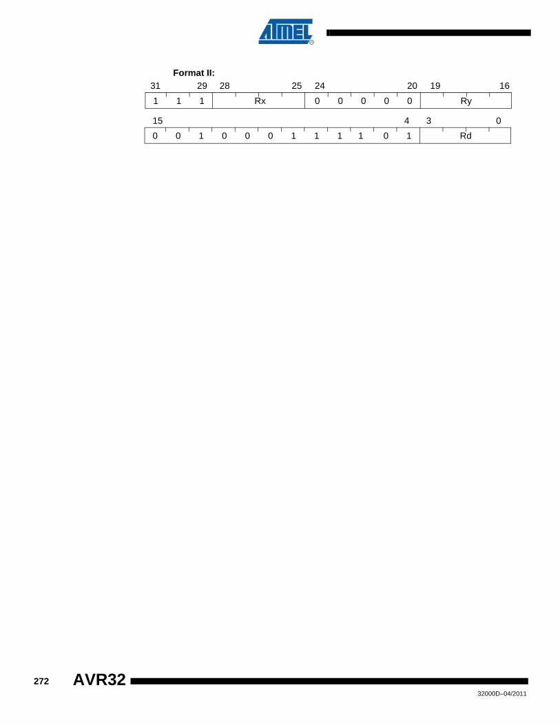
Format II:
1 1 1 0 0 0 0 0 Ry
31 29 28 25 24 20 19 16
0 0 1 0 0 0 1 1 1 1 0 1 Rd
15 4 3 0
Rx
27232000D–04/2011
AVR32

AVR32
PLSL.{B/H} – Packed Logical Shift Left
Architecture revision:Architecture revision1 and higher.
DescriptionPerform a logical shift left on each of the packed bytes or halfwords in the source register and store the result to the destination register.
Operation:I. Rd[31:24] ← LSL(Rs[31:24], sa3);
Rd[23:16] ← LSL(Rs[23:16], sa3); Rd[15:8] ← LSL(Rs[15:8], sa3);Rd[7:0] ← LSL(Rs[7:0], sa3);
II. Rd[31:16] ← LSL(Rs[31:16], sa4);Rd[15:0] ← LSL(Rs[15:0], sa4);
Syntax:I. plsl.b Rd, Rs, saII. plsl.h Rd, Rs, sa
Operands:I, II. {d, s} ∈ {0, 1, …, 15}I. sa ∈ {0, 1, …, 7}II. sa ∈ {0, 1, …, 15}
Status Flags:Q: Not affected.V: Not affected.N: Not affected.Z: Not affected.C: Not affected.
Opcode:
Format I:
1 1 1 0 0 0 0 0 0 sa3
31 29 28 25 24 19 18 16
0 0 1 0 0 1 0 0 0 0 1 0 Rd
15 4 3 0
Rs
27332000D–04/2011

Format II:
1 1 1 0 0 0 0 0 sa4
31 29 28 25 24 20 19 16
0 0 1 0 0 1 0 0 0 1 0 1 Rd
15 4 3 0
Rs
27432000D–04/2011
AVR32
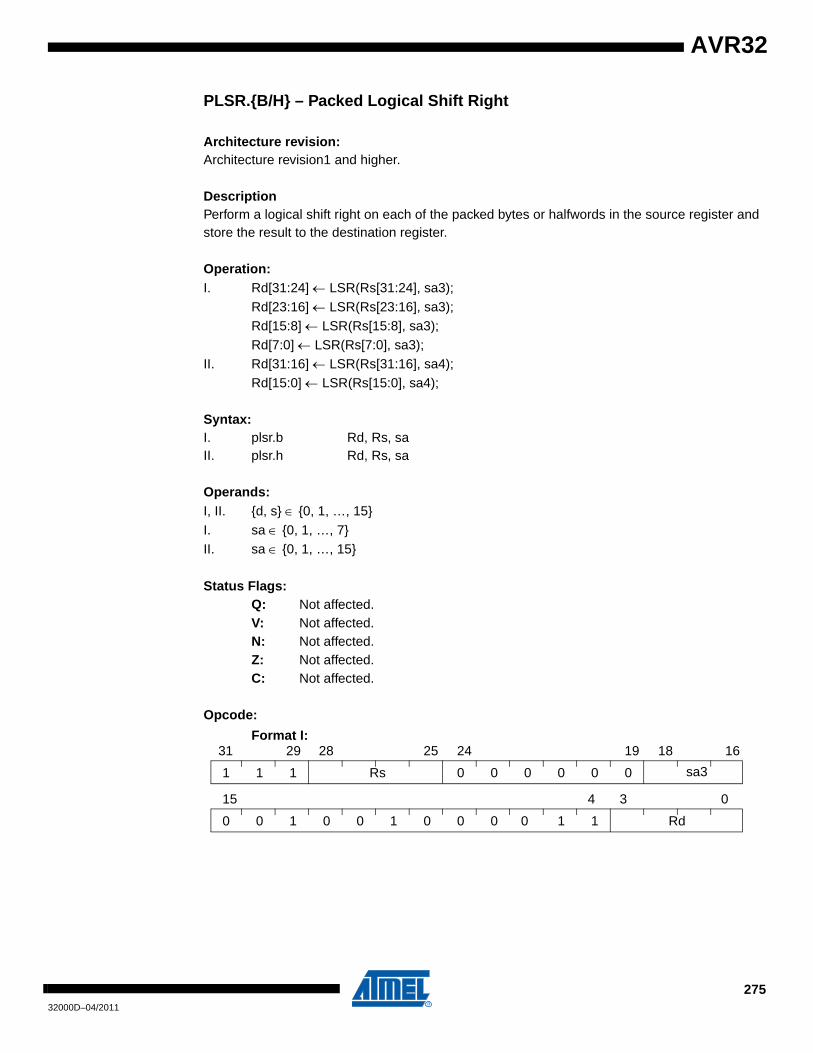
AVR32
PLSR.{B/H} – Packed Logical Shift Right
Architecture revision:Architecture revision1 and higher.
DescriptionPerform a logical shift right on each of the packed bytes or halfwords in the source register and store the result to the destination register.
Operation:I. Rd[31:24] ← LSR(Rs[31:24], sa3);
Rd[23:16] ← LSR(Rs[23:16], sa3); Rd[15:8] ← LSR(Rs[15:8], sa3);Rd[7:0] ← LSR(Rs[7:0], sa3);
II. Rd[31:16] ← LSR(Rs[31:16], sa4);Rd[15:0] ← LSR(Rs[15:0], sa4);
Syntax:I. plsr.b Rd, Rs, saII. plsr.h Rd, Rs, sa
Operands:I, II. {d, s} ∈ {0, 1, …, 15}I. sa ∈ {0, 1, …, 7}II. sa ∈ {0, 1, …, 15}
Status Flags:Q: Not affected.V: Not affected.N: Not affected.Z: Not affected.C: Not affected.
Opcode:
Format I:
1 1 1 0 0 0 0 0 0 sa3
31 29 28 25 24 19 18 16
0 0 1 0 0 1 0 0 0 0 1 1 Rd
15 4 3 0
Rs
27532000D–04/2011

Format II:
1 1 1 0 0 0 0 0 sa4
31 29 28 25 24 20 19 16
0 0 1 0 0 1 0 0 0 1 1 0 Rd
15 4 3 0
Rs
27632000D–04/2011
AVR32

AVR32
PMAX.{UB/SH} – Packed Maximum Value
Architecture revision:Architecture revision1 and higher.
DescriptionCompute the maximum values of pairs of packed unsigned bytes (pmax.ub) or packed signed halfwords (pmax.sh). Operation:I. If ( Rx[31:24] > Ry[31:24] ) then Rd[31:24] ← Rx[31:24] else Rd[31:24] ← Ry[31:24] ;
If ( Rx[23:16] > Ry[23:16] ) then Rd[23:16] ← Rx[23:16] else Rd[23:16] ← Ry[23:16] ;If ( Rx[15:8] > Ry[15:8] ) then Rd[15:8] ← Rx[15:8] else Rd[15:8] ← Ry[15:8] ;If ( Rx[7:0] > Ry[7:0] ) then Rd[7:0] ← Rx[7:0] else Rd[7:0] ← Ry[7:0] ;
II. If ( Rx[31:16] > Ry[31:16] ) then Rd[31:16] ← Rx[31:16] else Rd[31:16] ← Ry[31:16] ;If ( Rx[15:0] > Ry[15:0] ) then Rd[15:0] ← Rx[15:0] else Rd[15:0] ← Ry[15:0] ;
Syntax:I. pmax.ub Rd, Rx, RyII. pmax.sh Rd, Rx, RyOperands:I, II. {d, x, y} ∈ {0, 1, …, 15}
Status Flags:Format I:Q: Not affected.V: ( Rx[7:0] > Ry[7:0] )N: ( Rx[15:8] > Ry[15:8] )Z: ( Rx[23:16] > Ry[23:16] )C: ( Rx[31:24] > Ry[31:24] )Format II:Q: Not affected.V: Not affected.N: Not affected.Z: ( Rx[15:0] > Ry[15:0] )C: ( Rx[31:16] > Ry[31:16] )
Opcode:
Format I:
1 1 1 0 0 0 0 0 Ry
31 29 28 25 24 20 19 16
0 0 1 0 0 0 1 1 1 0 0 0 Rd
15 4 3 0
Rx
27732000D–04/2011

Format II:
1 1 1 0 0 0 0 0 Ry
31 29 28 25 24 20 19 16
0 0 1 0 0 0 1 1 1 0 0 1 Rd
15 4 3 0
Rx
27832000D–04/2011
AVR32
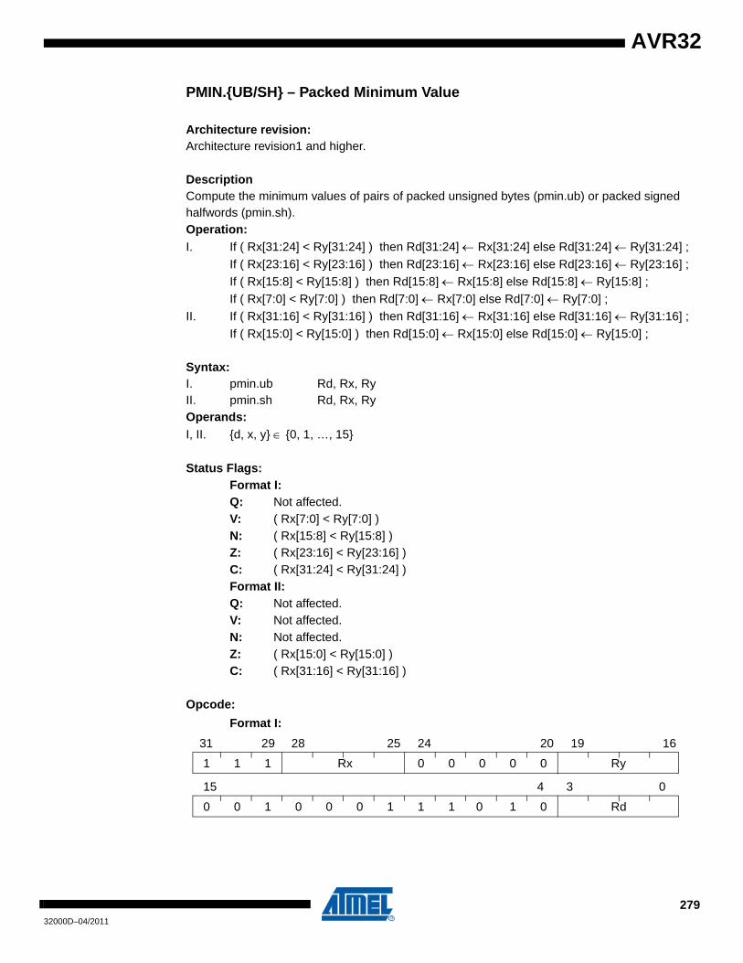
AVR32
PMIN.{UB/SH} – Packed Minimum Value
Architecture revision:Architecture revision1 and higher.
DescriptionCompute the minimum values of pairs of packed unsigned bytes (pmin.ub) or packed signed halfwords (pmin.sh). Operation:I. If ( Rx[31:24] < Ry[31:24] ) then Rd[31:24] ← Rx[31:24] else Rd[31:24] ← Ry[31:24] ;
If ( Rx[23:16] < Ry[23:16] ) then Rd[23:16] ← Rx[23:16] else Rd[23:16] ← Ry[23:16] ;If ( Rx[15:8] < Ry[15:8] ) then Rd[15:8] ← Rx[15:8] else Rd[15:8] ← Ry[15:8] ;If ( Rx[7:0] < Ry[7:0] ) then Rd[7:0] ← Rx[7:0] else Rd[7:0] ← Ry[7:0] ;
II. If ( Rx[31:16] < Ry[31:16] ) then Rd[31:16] ← Rx[31:16] else Rd[31:16] ← Ry[31:16] ;If ( Rx[15:0] < Ry[15:0] ) then Rd[15:0] ← Rx[15:0] else Rd[15:0] ← Ry[15:0] ;
Syntax:I. pmin.ub Rd, Rx, RyII. pmin.sh Rd, Rx, RyOperands:I, II. {d, x, y} ∈ {0, 1, …, 15}
Status Flags:Format I:Q: Not affected.V: ( Rx[7:0] < Ry[7:0] )N: ( Rx[15:8] < Ry[15:8] )Z: ( Rx[23:16] < Ry[23:16] )C: ( Rx[31:24] < Ry[31:24] )Format II:Q: Not affected.V: Not affected.N: Not affected.Z: ( Rx[15:0] < Ry[15:0] )C: ( Rx[31:16] < Ry[31:16] )
Opcode:
Format I:
1 1 1 0 0 0 0 0 Ry
31 29 28 25 24 20 19 16
0 0 1 0 0 0 1 1 1 0 1 0 Rd
15 4 3 0
Rx
27932000D–04/2011
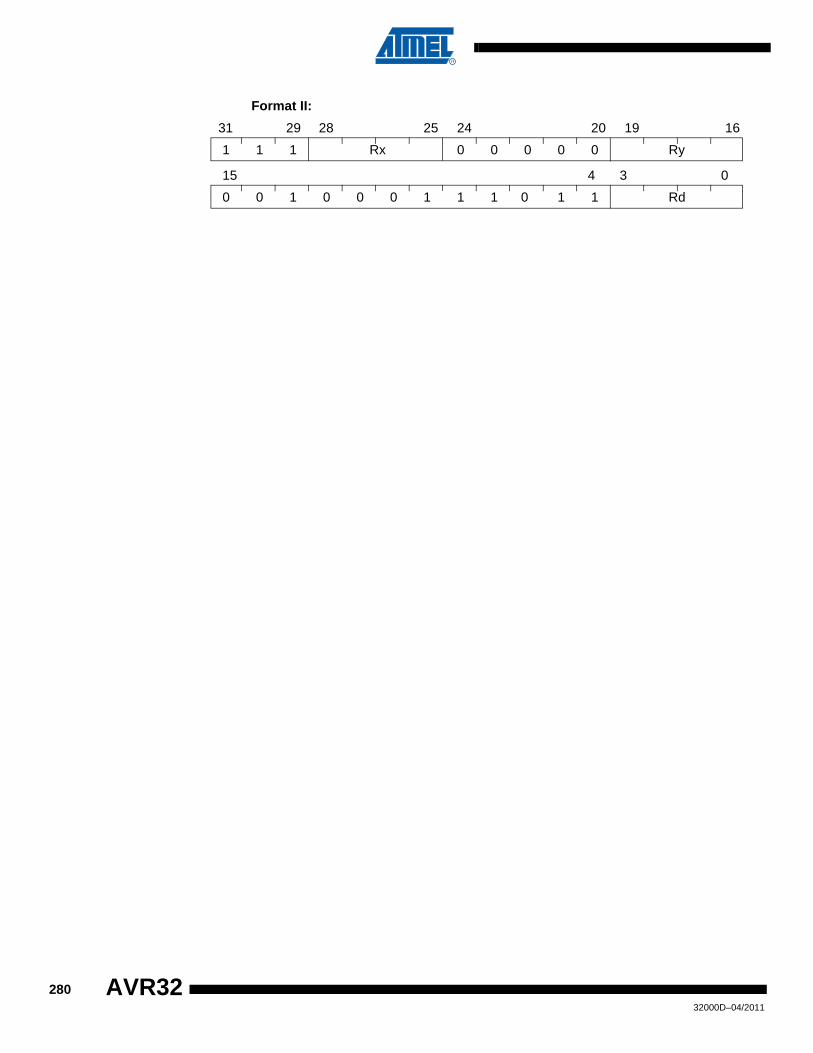
Format II:
1 1 1 0 0 0 0 0 Ry
31 29 28 25 24 20 19 16
0 0 1 0 0 0 1 1 1 0 1 1 Rd
15 4 3 0
Rx
28032000D–04/2011
AVR32
AVR32
POPJC – Pop Java Context from Frame
Architecture revision:Architecture revision1 and higher.
DescriptionFetch the system registers LV0 to LV7 used in Java state from the current method frame. The register FRAME (equal to R9) is used as pointer register.
Operation:I. temp ←FRAME;
JAVA_LV0 ←*(temp--);JAVA_LV1 ←*(temp--);JAVA_LV2 ←*(temp--);JAVA_LV3 ←*(temp--);JAVA_LV4 ←*(temp--);JAVA_LV5 ←*(temp--);JAVA_LV6 ←*(temp--);JAVA_LV7 ←*(temp--);
Syntax:I. popjc
Operands:I. none
Status Flags:Q: Not affected.V: Not affected.N: Not affected.Z: Not affected.C: Not affected.
Opcode:
1 1 0 1 0 1 1 1 0 0 0 1 0 0 1 1
15 9 8 4 3 0
28132000D–04/2011
POPM – Pop Multiple Registers from Stack
Architecture revision:Architecture revision1 and higher.
DescriptionLoads the consecutive words pointed to by SP into the registers specified in the instruction. The PC can be loaded, resulting in a jump to the loaded value. If PC is popped, the return value in R12 is tested and the flags are updated. R12 can optionally be updated with -1, 0 or 1. The k bit in the instruction coding is used to optionally let the POPM instruction update the return register R12 with the values -1, 0 or 1.
Operation:I. if Reglist8[PC] ∧ k == B’1
PC ← *(SP++)if Reglist8[LR:R12] == B’00
R12 ← 0;else if Reglist8[LR:R12] == B’01
R12 ← 1;else
R12 ← −1;Test R12 and update flags;
else if Reglist8[PC] == 1 then
PC ← *(SP++);if Reglist8[LR] == 1 then
LR ← *(SP++);if Reglist8[R12] == 1 then
R12 ←*(SP++);if Reglist8[PC] == 1 then
Test R12 and update flags;
if Reglist8[5] == 1 thenR11 ←*(SP++);
if Reglist8[4] == 1 thenR10 ←*(SP++);
if Reglist8[3] == 1 thenR9 ← *(SP++);R8 ← *(SP++);
if Reglist8[2] == 1 thenR7 ← *(SP++);R6 ← *(SP++);R5 ← *(SP++);R4 ← *(SP++);
if Reglist8[1] == 1 thenR3 ← *(SP++);
28232000D–04/2011
AVR32
AVR32
R2 ← *(SP++);R1 ← *(SP++);R0 ← *(SP++);
Syntax:I. popm Reglist8 {, R12 = {-1, 0, 1}}
If the optional R12 = {-1, 0, 1} parameter is specified, PC must be in Reglist8.If the optional R12 = {-1, 0, 1} parameter is specified, LR should NOT be in Reglist8.
Operands:I. Reglist8 ∈ {R0- R3, R4-R7, R8-R9, R10,R11, R12, LR, PC}
Status Flags:Flags are only updated if Reglist8[PC] == 1.They are set as the result of the operation cp R12, 0
Q: Not affectedV: V ← 0N: N ← RES[31]Z: Z ← (RES[31:0] == 0)C: C ← 0
Opcode:
Note:Emtpy Reglist8 gives UNDEFINED result.The R bit in the status register has no effect on this instruction.
1 1 0 1 PC LR 12 11 10 9-8 7-4 3-0 k 0 1 0
15 3 2 0
28332000D–04/2011

PREF – Cache Prefetch
Architecture revision:Architecture revision1 and higher.
DescriptionThis instruction allows the programmer to explicitly state that the cache should prefetch the specified line. The memory system treats this instruction in an implementation-dependent man-ner, and implementations without cache treats the instruction as a NOP. A prefetch instruction never reduces the performance of the system. If the prefetch instruction performs an action that would lower the system performance, it is treated as a NOP. For example, if the prefetch instruc-tion is about to generate an addressing exception, the instruction is cancelled and no exception is taken.
Operation:I. Prefetch cache line containing the address (Rp + SE(disp16)).
Syntax:pref Rp[disp]
Operands: I. p ∈ {0, 1, …, 15}
disp ∈ {-32768, -32767, ..., 32767}
Status Flags:Q: Not affected.V: Not affected.N: Not affected.Z: Not affected.C: Not affected.
Opcode:
1 1 1 1 0 1 0 0 0 0 1 Rp
31 29 28 20 19 16
disp16
15 0
0
28432000D–04/2011
AVR32
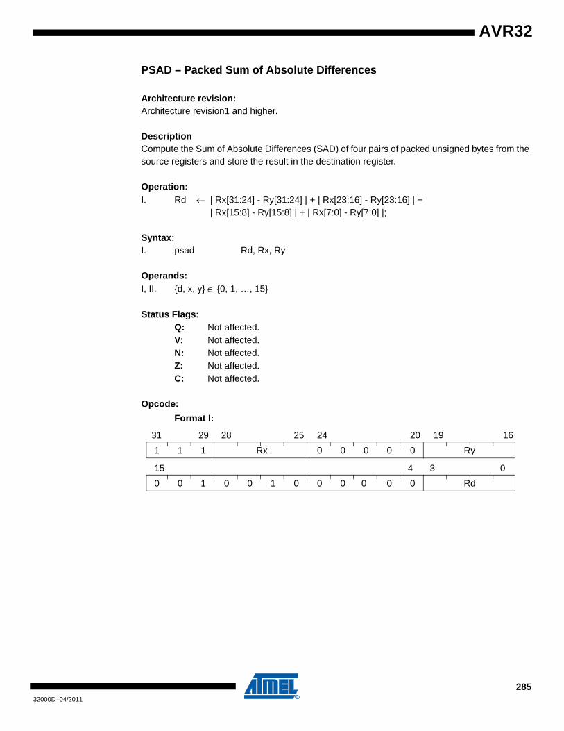
AVR32
PSAD – Packed Sum of Absolute Differences
Architecture revision:Architecture revision1 and higher.
DescriptionCompute the Sum of Absolute Differences (SAD) of four pairs of packed unsigned bytes from the source registers and store the result in the destination register.
Operation:I. Rd ← | Rx[31:24] - Ry[31:24] | + | Rx[23:16] - Ry[23:16] | +
| Rx[15:8] - Ry[15:8] | + | Rx[7:0] - Ry[7:0] |;
Syntax:I. psad Rd, Rx, Ry
Operands:I, II. {d, x, y} ∈ {0, 1, …, 15}
Status Flags:Q: Not affected.V: Not affected.N: Not affected.Z: Not affected.C: Not affected.
Opcode:
Format I:
1 1 1 0 0 0 0 0 Ry
31 29 28 25 24 20 19 16
0 0 1 0 0 1 0 0 0 0 0 0 Rd
15 4 3 0
Rx
28532000D–04/2011
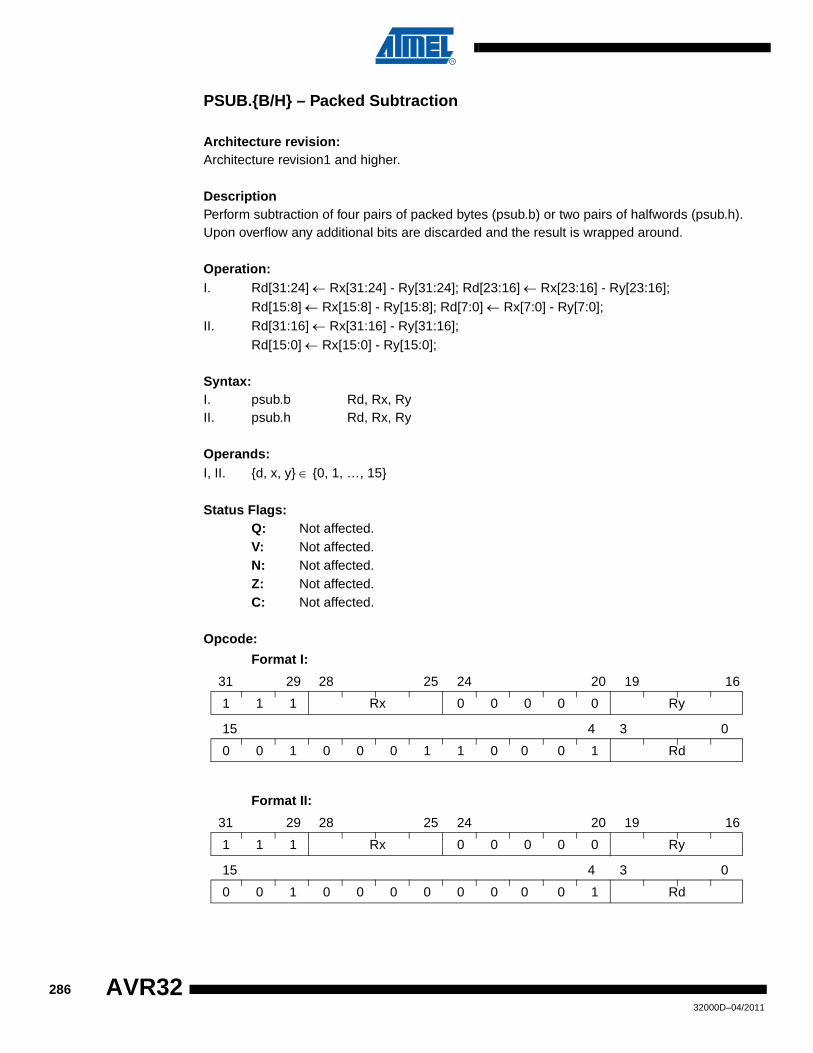
PSUB.{B/H} – Packed Subtraction
Architecture revision:Architecture revision1 and higher.
DescriptionPerform subtraction of four pairs of packed bytes (psub.b) or two pairs of halfwords (psub.h). Upon overflow any additional bits are discarded and the result is wrapped around.
Operation:I. Rd[31:24] ← Rx[31:24] - Ry[31:24]; Rd[23:16] ← Rx[23:16] - Ry[23:16];
Rd[15:8] ← Rx[15:8] - Ry[15:8]; Rd[7:0] ← Rx[7:0] - Ry[7:0];II. Rd[31:16] ← Rx[31:16] - Ry[31:16];
Rd[15:0] ← Rx[15:0] - Ry[15:0];
Syntax:I. psub.b Rd, Rx, RyII. psub.h Rd, Rx, Ry
Operands:I, II. {d, x, y} ∈ {0, 1, …, 15}
Status Flags:Q: Not affected.V: Not affected.N: Not affected.Z: Not affected.C: Not affected.
Opcode:
Format I:
Format II:
1 1 1 0 0 0 0 0 Ry
31 29 28 25 24 20 19 16
0 0 1 0 0 0 1 1 0 0 0 1 Rd
15 4 3 0
Rx
1 1 1 0 0 0 0 0 Ry
31 29 28 25 24 20 19 16
0 0 1 0 0 0 0 0 0 0 0 1 Rd
15 4 3 0
Rx
28632000D–04/2011
AVR32
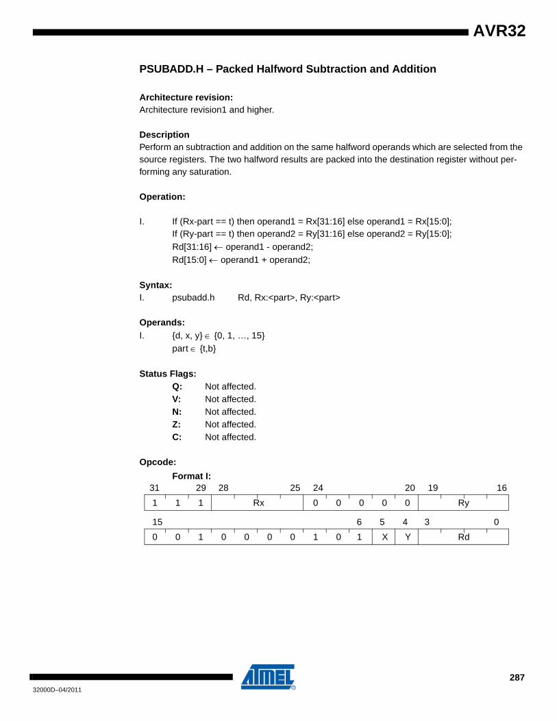
AVR32
PSUBADD.H – Packed Halfword Subtraction and Addition
Architecture revision:Architecture revision1 and higher.
DescriptionPerform an subtraction and addition on the same halfword operands which are selected from the source registers. The two halfword results are packed into the destination register without per-forming any saturation.
Operation:
I. If (Rx-part == t) then operand1 = Rx[31:16] else operand1 = Rx[15:0];If (Ry-part == t) then operand2 = Ry[31:16] else operand2 = Ry[15:0];Rd[31:16] ← operand1 - operand2;Rd[15:0] ← operand1 + operand2;
Syntax:I. psubadd.h Rd, Rx:<part>, Ry:<part>
Operands:I. {d, x, y} ∈ {0, 1, …, 15}
part ∈ {t,b}
Status Flags:Q: Not affected.V: Not affected.N: Not affected.Z: Not affected.C: Not affected.
Opcode:
Format I:
1 1 1 0 0 0 0 0 Ry
31 29 28 25 24 20 19 16
0 0 1 0 0 0 0 1 0 1 X Y Rd
15 6 5 4 3 0
Rx
28732000D–04/2011
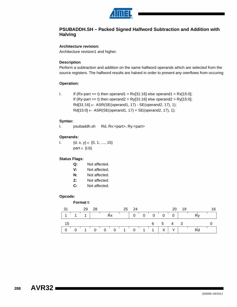
PSUBADDH.SH – Packed Signed Halfword Subtraction and Addition with Halving
Architecture revision:Architecture revision1 and higher.
DescriptionPerform a subtraction and addition on the same halfword operands which are selected from the source registers. The halfword results are halved in order to prevent any overflows from occuring
Operation:
I. If (Rx-part == t) then operand1 = Rx[31:16] else operand1 = Rx[15:0];If (Ry-part == t) then operand2 = Ry[31:16] else operand2 = Ry[15:0];Rd[31:16] ← ASR(SE(operand1, 17) - SE(operand2, 17), 1);Rd[15:0] ← ASR(SE(operand1, 17) + SE(operand2, 17), 1);
Syntax:I. psubaddh.sh Rd, Rx:<part>, Ry:<part>
Operands:I. {d, x, y} ∈ {0, 1, …, 15}
part ∈ {t,b}
Status Flags:Q: Not affected.V: Not affected.N: Not affected.Z: Not affected.C: Not affected.
Opcode:
Format I:
1 1 1 0 0 0 0 0 Ry
31 29 28 25 24 20 19 16
0 0 1 0 0 0 1 0 1 1 X Y Rd
15 6 5 4 3 0
Rx
28832000D–04/2011
AVR32
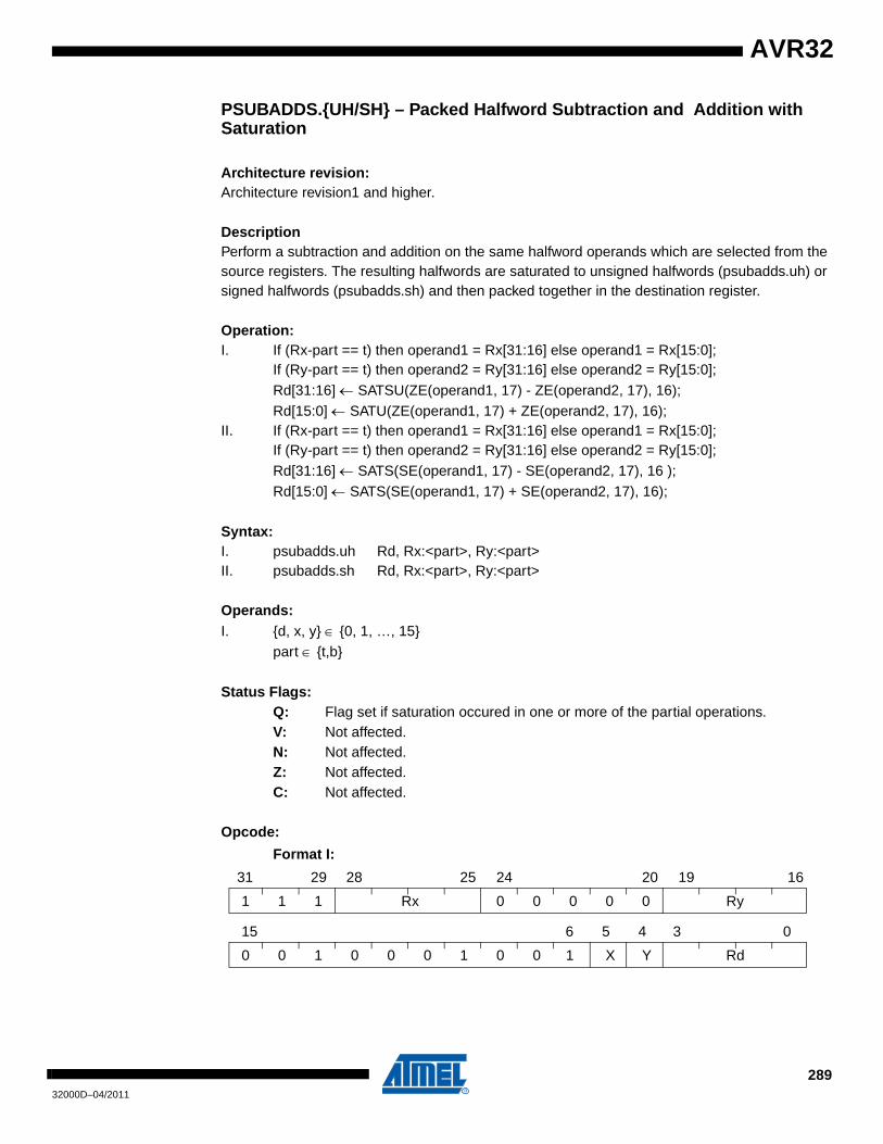
AVR32
PSUBADDS.{UH/SH} – Packed Halfword Subtraction and Addition with Saturation
Architecture revision:Architecture revision1 and higher.
DescriptionPerform a subtraction and addition on the same halfword operands which are selected from the source registers. The resulting halfwords are saturated to unsigned halfwords (psubadds.uh) or signed halfwords (psubadds.sh) and then packed together in the destination register.
Operation:I. If (Rx-part == t) then operand1 = Rx[31:16] else operand1 = Rx[15:0];
If (Ry-part == t) then operand2 = Ry[31:16] else operand2 = Ry[15:0];Rd[31:16] ← SATSU(ZE(operand1, 17) - ZE(operand2, 17), 16);Rd[15:0] ← SATU(ZE(operand1, 17) + ZE(operand2, 17), 16);
II. If (Rx-part == t) then operand1 = Rx[31:16] else operand1 = Rx[15:0];If (Ry-part == t) then operand2 = Ry[31:16] else operand2 = Ry[15:0];Rd[31:16] ← SATS(SE(operand1, 17) - SE(operand2, 17), 16 );Rd[15:0] ← SATS(SE(operand1, 17) + SE(operand2, 17), 16);
Syntax:I. psubadds.uh Rd, Rx:<part>, Ry:<part>II. psubadds.sh Rd, Rx:<part>, Ry:<part>
Operands:I. {d, x, y} ∈ {0, 1, …, 15}
part ∈ {t,b}
Status Flags:Q: Flag set if saturation occured in one or more of the partial operations.V: Not affected.N: Not affected.Z: Not affected.C: Not affected.
Opcode:
Format I:
1 1 1 0 0 0 0 0 Ry
31 29 28 25 24 20 19 16
0 0 1 0 0 0 1 0 0 1 X Y Rd
15 6 5 4 3 0
Rx
28932000D–04/2011

Format II:
1 1 1 0 0 0 0 0 Ry
31 29 28 25 24 20 19 16
0 0 1 0 0 0 0 1 1 1 X Y Rd
15 6 5 4 3 0
Rx
29032000D–04/2011
AVR32

AVR32
PSUBH.{UB/SH} – Packed Subtraction with Halving
Architecture revision:Architecture revision1 and higher.
DescriptionPerform subtraction of four pairs of packed unsigned bytes (psub.ub) or two pairs of signed half-words (psub.sh) with a halfing of the result to prevent any overflows from occuring.
Operation:I. Rd[31:24] ← LSR(ZE(Rx[31:24], 9) - ZE(Ry[31:24], 9), 1);
Rd[23:16] ← LSR(ZE(Rx[23:16], 9) - ZE(Ry[23:16], 9), 1);Rd[15:8] ← LSR(ZE(Rx[15:8], 9) - ZE(Ry[15:8], 9), 1); Rd[7:0] ← LSR(ZE(Rx[7:0], 9) - ZE(Ry[7:0], 9), 1);
II. Rd[31:16] ← ASR(SE(Rx[31:16], 17) - SE(Ry[31:16], 17), 1);Rd[15:0] ← ASR(SE(Rx[15:0], 17) - SE(Ry[15:0], 17), 1);
Syntax:I. psubh.ub Rd, Rx, RyII. psubh.sh Rd, Rx, Ry
Operands:I, II. {d, x, y} ∈ {0, 1, …, 15}
Status Flags:Q: Not affected.V: Not affected.N: Not affected.Z: Not affected.C: Not affected.
Opcode:
Format I:
Format II:
1 1 1 0 0 0 0 0 Ry
31 29 28 25 24 20 19 16
0 0 1 0 0 0 1 1 0 1 1 1 Rd
15 4 3 0
Rx
1 1 1 0 0 0 0 0 Ry
31 29 28 25 24 20 19 16
0 0 1 0 0 0 0 0 1 1 0 1 Rd
15 4 3 0
Rx
29132000D–04/2011
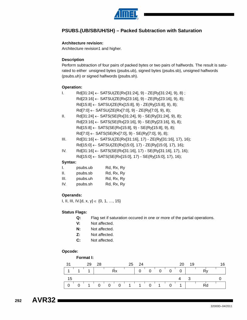
PSUBS.{UB/SB/UH/SH} – Packed Subtraction with Saturation
Architecture revision:Architecture revision1 and higher.
DescriptionPerform subtraction of four pairs of packed bytes or two pairs of halfwords. The result is satu-rated to either unsigned bytes (psubs.ub), signed bytes (psubs.sb), unsigned halfwords (psubs.uh) or signed halfwords (psubs.sh).
Operation:I. Rd[31:24] ← SATSU(ZE(Rx[31:24], 9) - ZE(Ry[31:24], 9), 8) ;
Rd[23:16] ← SATSU(ZE(Rx[23:16], 9) - ZE(Ry[23:16], 9), 8);Rd[15:8] ← SATSU(ZE(Rx[15:8], 9) - ZE(Ry[15:8], 9), 8); Rd[7:0] ← SATSU(ZE(Rx[7:0], 9) - ZE(Ry[7:0], 9), 8);
II. Rd[31:24] ← SATS(SE(Rx[31:24], 9) - SE(Ry[31:24], 9), 8); Rd[23:16] ← SATS(SE(Rx[23:16], 9) - SE(Ry[23:16], 9), 8);Rd[15:8] ← SATS(SE(Rx[15:8], 9) - SE(Ry[15:8], 9), 8); Rd[7:0] ← SATS(SE(Rx[7:0], 9) - SE(Ry[7:0], 9), 8);
III. Rd[31:16] ← SATSU(ZE(Rx[31:16], 17) - ZE(Ry[31:16], 17), 16);Rd[15:0] ← SATSU(ZE(Rx[15:0], 17) - ZE(Ry[15:0], 17), 16);
IV. Rd[31:16] ← SATS(SE(Rx[31:16], 17) - SE(Ry[31:16], 17), 16);Rd[15:0] ← SATS(SE(Rx[15:0], 17) - SE(Ry[15:0], 17), 16);
Syntax:I. psubs.ub Rd, Rx, RyII. psubs.sb Rd, Rx, RyIII. psubs.uh Rd, Rx, RyIV. psubs.sh Rd, Rx, Ry
Operands:I, II, III, IV.{d, x, y} ∈ {0, 1, …, 15}
Status Flags:Q: Flag set if saturation occured in one or more of the partial operations.V: Not affected.N: Not affected.Z: Not affected.C: Not affected.
Opcode:
Format I:
1 1 1 0 0 0 0 0 Ry
31 29 28 25 24 20 19 16
0 0 1 0 0 0 1 1 0 1 0 1 Rd
15 4 3 0
Rx
29232000D–04/2011
AVR32
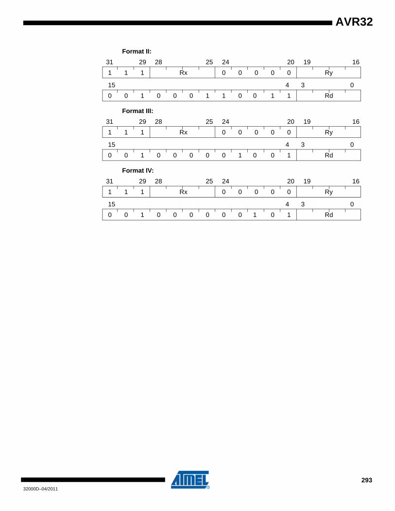
AVR32
Format II:
Format III:
Format IV:
1 1 1 0 0 0 0 0 Ry
31 29 28 25 24 20 19 16
0 0 1 0 0 0 1 1 0 0 1 1 Rd
15 4 3 0
Rx
1 1 1 0 0 0 0 0 Ry
31 29 28 25 24 20 19 16
0 0 1 0 0 0 0 0 1 0 0 1 Rd
15 4 3 0
Rx
1 1 1 0 0 0 0 0 Ry
31 29 28 25 24 20 19 16
0 0 1 0 0 0 0 0 0 1 0 1 Rd
15 4 3 0
Rx
29332000D–04/2011
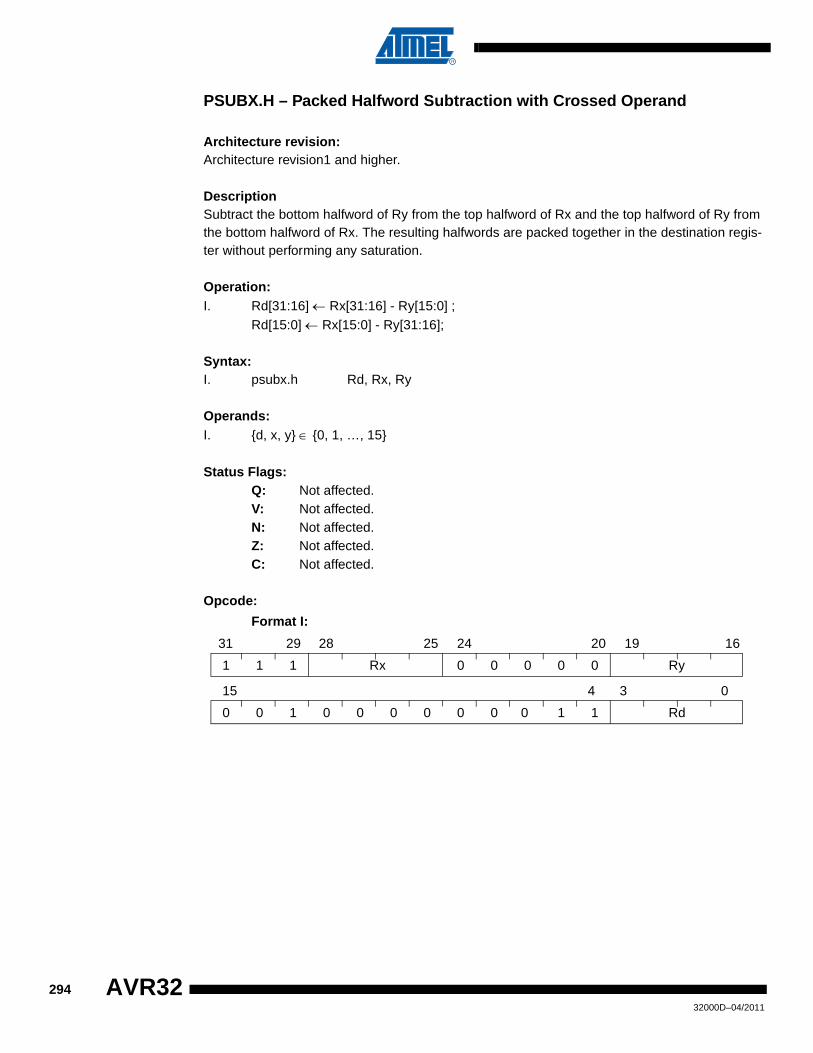
PSUBX.H – Packed Halfword Subtraction with Crossed Operand
Architecture revision:Architecture revision1 and higher.
DescriptionSubtract the bottom halfword of Ry from the top halfword of Rx and the top halfword of Ry from the bottom halfword of Rx. The resulting halfwords are packed together in the destination regis-ter without performing any saturation.
Operation:I. Rd[31:16] ← Rx[31:16] - Ry[15:0] ;
Rd[15:0] ← Rx[15:0] - Ry[31:16];
Syntax:I. psubx.h Rd, Rx, Ry
Operands:I. {d, x, y} ∈ {0, 1, …, 15}
Status Flags:Q: Not affected.V: Not affected.N: Not affected.Z: Not affected.C: Not affected.
Opcode:
Format I:
1 1 1 0 0 0 0 0 Ry
31 29 28 25 24 20 19 16
0 0 1 0 0 0 0 0 0 0 1 1 Rd
15 4 3 0
Rx
29432000D–04/2011
AVR32

AVR32
PSUBXH.SH – Packed Signed Halfword Subtraction with Crossed Operand and Halving
Architecture revision:Architecture revision1 and higher.
DescriptionSubtract the bottom halfword of Ry from the top halfword of Rx and the top halfword of Ry from the bottom halfword of Rx. The resulting halfwords are halved in order to avoid any overflow and then packed together in the destination register.
Operation:I. Rd[31:16] ← ASR(SE(Rx[31:16], 17) - SE(Ry[15:0], 17), 1);
Rd[15:0] ← ASR(SE(Rx[15:0], 17) - SE(Ry[31:16], 17), 1);
Syntax:I. psubxh.sh Rd, Rx, Ry
Operands:I. {d, x, y} ∈ {0, 1, …, 15}
Status Flags:Q: Not affected.V: Not affected.N: Not affected.Z: Not affected.C: Not affected.
Opcode:
Format I:
1 1 1 0 0 0 0 0 Ry
31 29 28 25 24 20 19 16
0 0 1 0 0 0 0 0 1 1 1 1 Rd
15 4 3 0
Rx
29532000D–04/2011
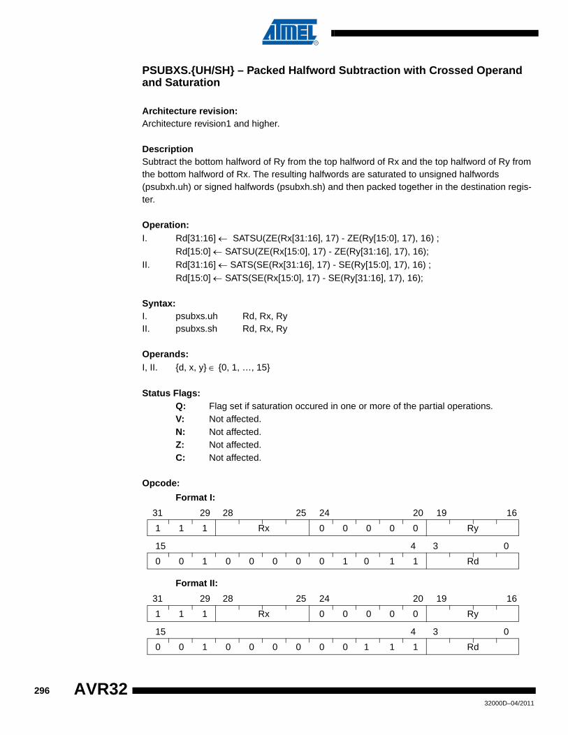
PSUBXS.{UH/SH} – Packed Halfword Subtraction with Crossed Operand and Saturation
Architecture revision:Architecture revision1 and higher.
DescriptionSubtract the bottom halfword of Ry from the top halfword of Rx and the top halfword of Ry from the bottom halfword of Rx. The resulting halfwords are saturated to unsigned halfwords (psubxh.uh) or signed halfwords (psubxh.sh) and then packed together in the destination regis-ter.
Operation:I. Rd[31:16] ← SATSU(ZE(Rx[31:16], 17) - ZE(Ry[15:0], 17), 16) ;
Rd[15:0] ← SATSU(ZE(Rx[15:0], 17) - ZE(Ry[31:16], 17), 16);II. Rd[31:16] ← SATS(SE(Rx[31:16], 17) - SE(Ry[15:0], 17), 16) ;
Rd[15:0] ← SATS(SE(Rx[15:0], 17) - SE(Ry[31:16], 17), 16);
Syntax:I. psubxs.uh Rd, Rx, RyII. psubxs.sh Rd, Rx, Ry
Operands:I, II. {d, x, y} ∈ {0, 1, …, 15}
Status Flags:Q: Flag set if saturation occured in one or more of the partial operations.V: Not affected.N: Not affected.Z: Not affected.C: Not affected.
Opcode:
Format I:
Format II:
1 1 1 0 0 0 0 0 Ry
31 29 28 25 24 20 19 16
0 0 1 0 0 0 0 0 1 0 1 1 Rd
15 4 3 0
Rx
1 1 1 0 0 0 0 0 Ry
31 29 28 25 24 20 19 16
0 0 1 0 0 0 0 0 0 1 1 1 Rd
15 4 3 0
Rx
29632000D–04/2011
AVR32
AVR32
29732000D–04/2011
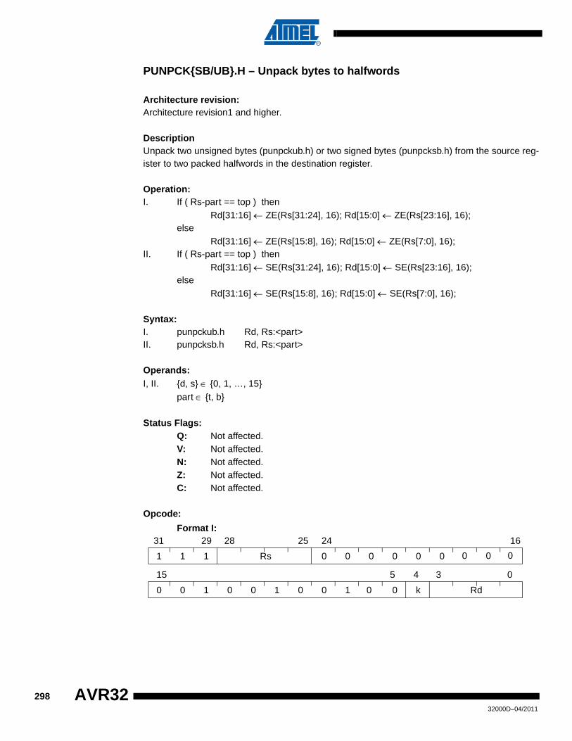
PUNPCK{SB/UB}.H – Unpack bytes to halfwords
Architecture revision:Architecture revision1 and higher.
DescriptionUnpack two unsigned bytes (punpckub.h) or two signed bytes (punpcksb.h) from the source reg-ister to two packed halfwords in the destination register.
Operation:I. If ( Rs-part == top ) then
Rd[31:16] ← ZE(Rs[31:24], 16); Rd[15:0] ← ZE(Rs[23:16], 16);else
Rd[31:16] ← ZE(Rs[15:8], 16); Rd[15:0] ← ZE(Rs[7:0], 16);II. If ( Rs-part == top ) then
Rd[31:16] ← SE(Rs[31:24], 16); Rd[15:0] ← SE(Rs[23:16], 16);else
Rd[31:16] ← SE(Rs[15:8], 16); Rd[15:0] ← SE(Rs[7:0], 16); Syntax:I. punpckub.h Rd, Rs:<part>II. punpcksb.h Rd, Rs:<part>
Operands:I, II. {d, s} ∈ {0, 1, …, 15}
part ∈ {t, b}
Status Flags:Q: Not affected.V: Not affected.N: Not affected.Z: Not affected.C: Not affected.
Opcode:
Format I:
1 1 1 0 0 0 0 0 0 0 0
31 29 28 25 24 16
0 0 1 0 0 1 0 0 1 0 0 k Rd
15 5 4 3 0
Rs 0
29832000D–04/2011
AVR32

AVR32
Format II:
1 1 1 0 0 0 0 0 0 0 0
31 29 28 25 24 16
0 0 1 0 0 1 0 0 1 0 1 k Rd
15 5 4 3 0
Rs 0
29932000D–04/2011
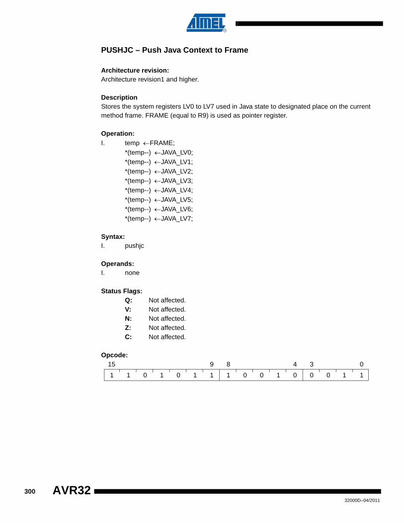
PUSHJC – Push Java Context to Frame
Architecture revision:Architecture revision1 and higher.
DescriptionStores the system registers LV0 to LV7 used in Java state to designated place on the current method frame. FRAME (equal to R9) is used as pointer register.
Operation:I. temp ←FRAME;
*(temp--) ←JAVA_LV0;*(temp--) ←JAVA_LV1;*(temp--) ←JAVA_LV2;*(temp--) ←JAVA_LV3;*(temp--) ←JAVA_LV4;*(temp--) ←JAVA_LV5;*(temp--) ←JAVA_LV6;*(temp--) ←JAVA_LV7;
Syntax:I. pushjc
Operands:I. none
Status Flags:Q: Not affected.V: Not affected.N: Not affected.Z: Not affected.C: Not affected.
Opcode:
1 1 0 1 0 1 1 1 0 0 1 0 0 0 1 1
15 9 8 4 3 0
30032000D–04/2011
AVR32
AVR32
PUSHM – Push Multiple Registers to Stack
Architecture revision:Architecture revision1 and higher.
DescriptionStores the registers specified in the instruction into consecutive words pointed to by SP.
Operation:I. if Reglist8[0] == 1 then
*(--SP) ←R0;*(--SP) ←R1;*(--SP) ←R2;*(--SP) ←R3;
if Reglist8[1] == 1 then*(--SP) ←R4;*(--SP) ←R5;*(--SP) ←R6;*(--SP) ←R7;
if Reglist8[2] == 1 then*(--SP) ←R8;*(--SP) ←R9;
if Reglist8[3] == 1 then*(--SP) ←R10;
if Reglist8[4] == 1 then*(--SP) ←R11;
if Reglist8[5] == 1 then*(--SP) ←R12;
if Reglist8[6] == 1 then*(--SP) ←LR;
if Reglist8[7] == 1 then*(--SP) ←PC;
Syntax:I. pushm Reglist8
Operands:I. Reglist8 ∈ {R0- R3, R4-R7, R8-R9, R10,R11, R12, LR, PC}
Status Flags:Q: Not affected.V: Not affected.N: Not affected.Z: Not affected.C: Not affected.
30132000D–04/2011

Opcode:
Note:Emtpy Reglist8 gives UNDEFINED result.The R bit in the status register has no effect on this instruction.
1 1 0 1 PC LR 12 11 10 9-8 7-4 3-0 0 0 0 1
15 13 12 11 4 3 0
30232000D–04/2011
AVR32
AVR32
RCALL – Relative Subroutine Call
Architecture revision:Architecture revision1 and higher.
DescriptionPC-relative call of subroutine
Operation:I. LR ← PC + 2
PC ← PC + (SE(disp10)<<1)II. LR ← PC + 4
PC ← PC + (SE(disp21)<<1)
Syntax:I. rcall PC[disp]II. rcall PC[disp]
Operands:I. disp ∈ {-1024, -1022, ..., 1022}II. disp ∈ {-2097152, -2097150, ..., 2097150}
Status FlagsQ: Not affected.V: Not affected.N: Not affected.Z: Not affected.C: Not affected.
Opcode:
Format I:
Format II:
1 1 0 0 disp10[7:0] 1 1 d10[9:8]
15 13 12 11 4 3 2 1 0
1 1 1 disp21[20:17] 0 1 0 1K21
0 0 0
31 29 28 25 24 21 20 19 16
disp21[15:0]
15 0
0[16]
30332000D–04/2011
RET{cond4} – Conditional Return from Subroutine
Architecture revision:Architecture revision1 and higher.
DescriptionReturn from subroutine if the specified condition is true. Values are moved into the return regis-ter, the return value is tested, and flags are set.
Operation:I. If (cond4)
If (Rs != {LR, SP, PC})R12 ← Rs;
else if (Rs == LR)R12 ← -1;
else if (Rs == SP)R12 ← 0;
elseR12 ← 1;
Test R12 and set flags;PC ← LR;
Syntax:I. ret{cond4} Rs
Operands:I. cond4 ∈ {eq, ne, cc/hs, cs/lo, ge, lt, mi, pl, ls, gt, le, hi, vs, vc, qs, al}
s ∈{0, 1, …, 15}
Status Flags:Flags are set as result of the operation CP R12, 0.Q: Not affectedV: V ← 0N: N ← RES[31]Z: Z ← (RES[31:0] == 0)C: C ← 0
Opcode:
0 1 0 1 1 1 1 0 cond4 Rs
15 13 12 9 8 7 4 3 0
30432000D–04/2011
AVR32

AVR32
RETD – Return from Debug mode
Architecture revision:Architecture revision1 and higher.
DescriptionReturn from debug mode.
Operation:I. SR ← RSR_DBG
PC ← RAR_DBG
Syntax:I. retd
Operands:None
Status Flags:Q: Not affectedV: Not affectedN: Not affectedZ: Not affectedC: Not affected
Opcode:
Note:
This instruction can only be executed in a privileged mode. Execution from any other mode willtrigger a Privilege Violation exception.
1 1 0 1 0 1 1 0 0 0 1 0 0 0 1 1
15 9 8 4 3 0
30532000D–04/2011
RETE – Return from event handler
Architecture revision:Architecture revision1 and higher.
Description
Returns from an exception or interrupt. SREG[L] is cleared to support atomical memory accesswith the stcond instruction. This instruction can only be executed in INT0-INT3, EX and NMImodes. Execution in Application or Supervisor modes will trigger a Privilege Violation exception.
Operation:
I. If (microarchitecture == AVR32A)
SR ← *(SPSYS++)
PC ← *(SPSYS++)
If ( SR[M2:M0] == {B’010, B’011, B’100, B’101} )
LR ← *(SPSYS++)
R12 ← *(SPSYS++)
R11 ← *(SPSYS++)
R10 ← *(SPSYS++)
R9 ← *(SPSYS++)
R8 ← *(SPSYS++)
SREG[L] ← 0;
elseSR ← RSRCurrent Context
PC ← RARCurrent Context
SREG[L] ← 0;
Syntax:
I RETE
Operands:
None
Status FlagsQ: Not affectedV: Not affectedN: Not affectedZ: Not affectedC: Not affected
30632000D–04/2011
AVR32
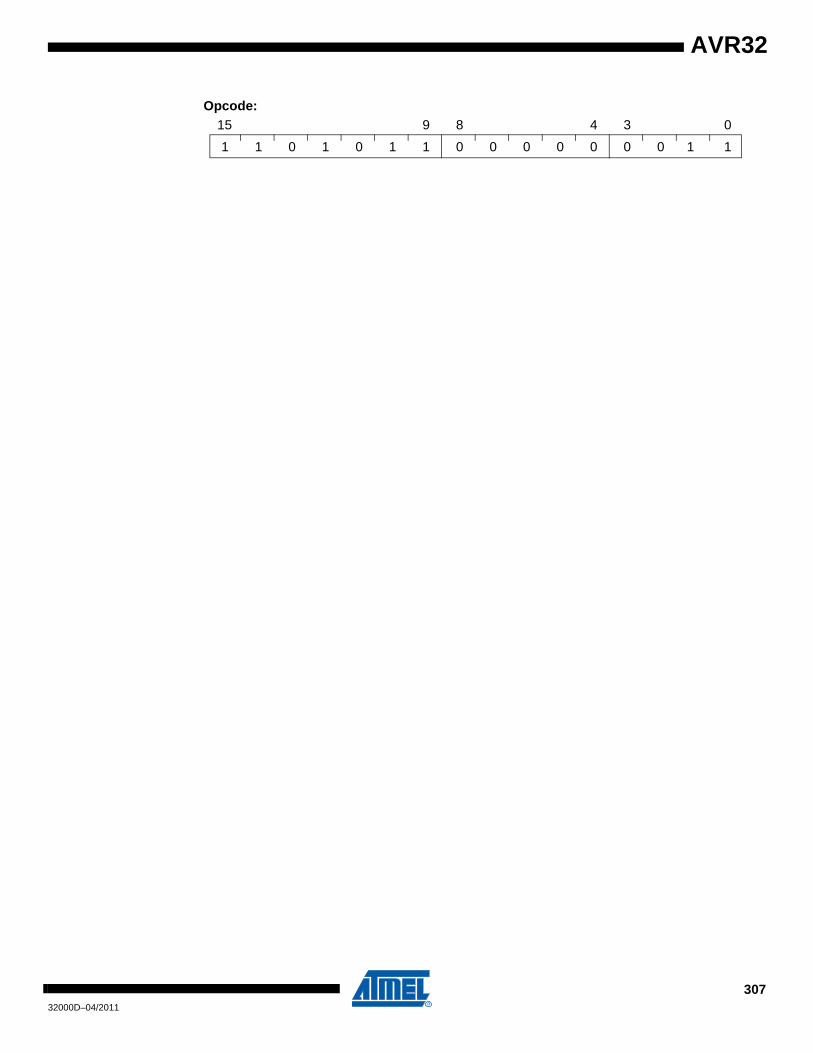
AVR32
Opcode:
1 1 0 1 0 1 1 0 0 0 0 0 0 0 1 1
15 9 8 4 3 0
30732000D–04/2011
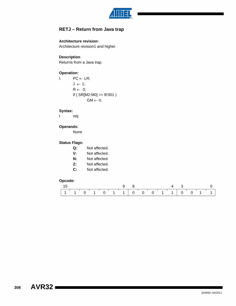
RETJ – Return from Java trap
Architecture revision:Architecture revision1 and higher.
DescriptionReturns from a Java trap.
Operation:I. PC ← LR;
J ← 1;R ← 0;if ( SR[M2:M0] == B’001 )
GM ← 0;
Syntax:I retj
Operands:None
Status Flags:Q: Not affected.V: Not affected.N: Not affected.Z: Not affected.C: Not affected.
Opcode:
1 1 0 1 0 1 1 0 0 0 1 1 0 0 1 1
15 9 8 4 3 0
30832000D–04/2011
AVR32
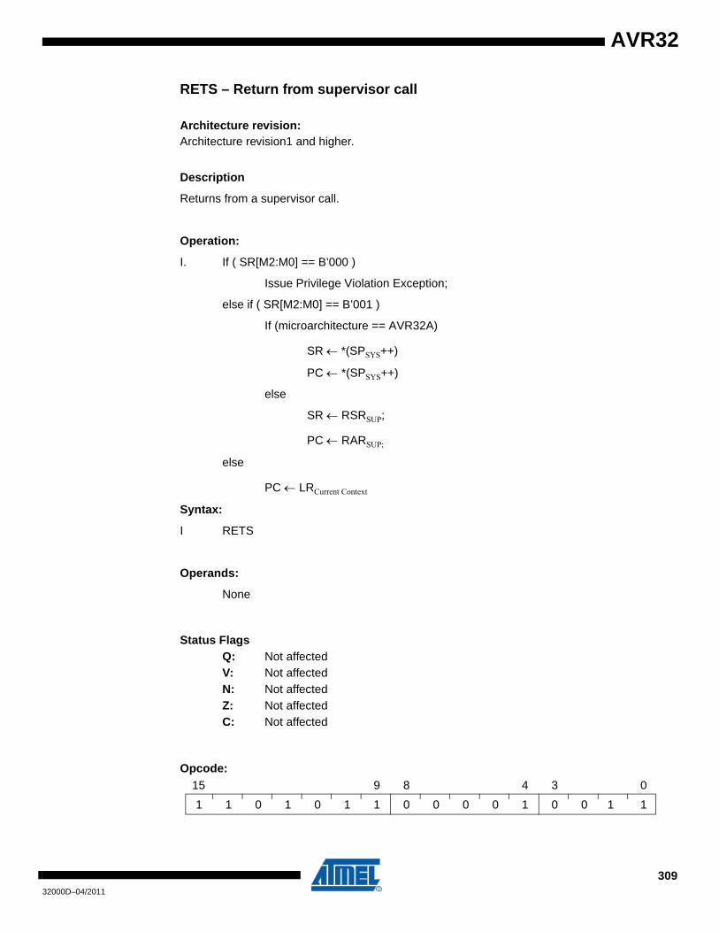
AVR32
RETS – Return from supervisor call
Architecture revision:Architecture revision1 and higher.
Description
Returns from a supervisor call.
Operation:
I. If ( SR[M2:M0] == B’000 )
Issue Privilege Violation Exception;
else if ( SR[M2:M0] == B’001 )
If (microarchitecture == AVR32A)
SR ← *(SPSYS++)
PC ← *(SPSYS++)
else
SR ← RSRSUP;
PC ← RARSUP;
else
PC ← LRCurrent Context
Syntax:
I RETS
Operands:
None
Status FlagsQ: Not affectedV: Not affectedN: Not affectedZ: Not affectedC: Not affected
Opcode:
1 1 0 1 0 1 1 0 0 0 0 1 0 0 1 1
15 9 8 4 3 0
30932000D–04/2011
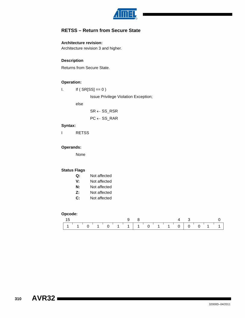
RETSS – Return from Secure State
Architecture revision:Architecture revision 3 and higher.
Description
Returns from Secure State.
Operation:
I. If ( SR[SS] == 0 )
Issue Privilege Violation Exception;
else
SR ← SS_RSR
PC ← SS_RAR
Syntax:
I RETSS
Operands:
None
Status FlagsQ: Not affectedV: Not affectedN: Not affectedZ: Not affectedC: Not affected
Opcode:
1 1 0 1 0 1 1 1 0 1 1 0 0 0 1 1
15 9 8 4 3 0
31032000D–04/2011
AVR32
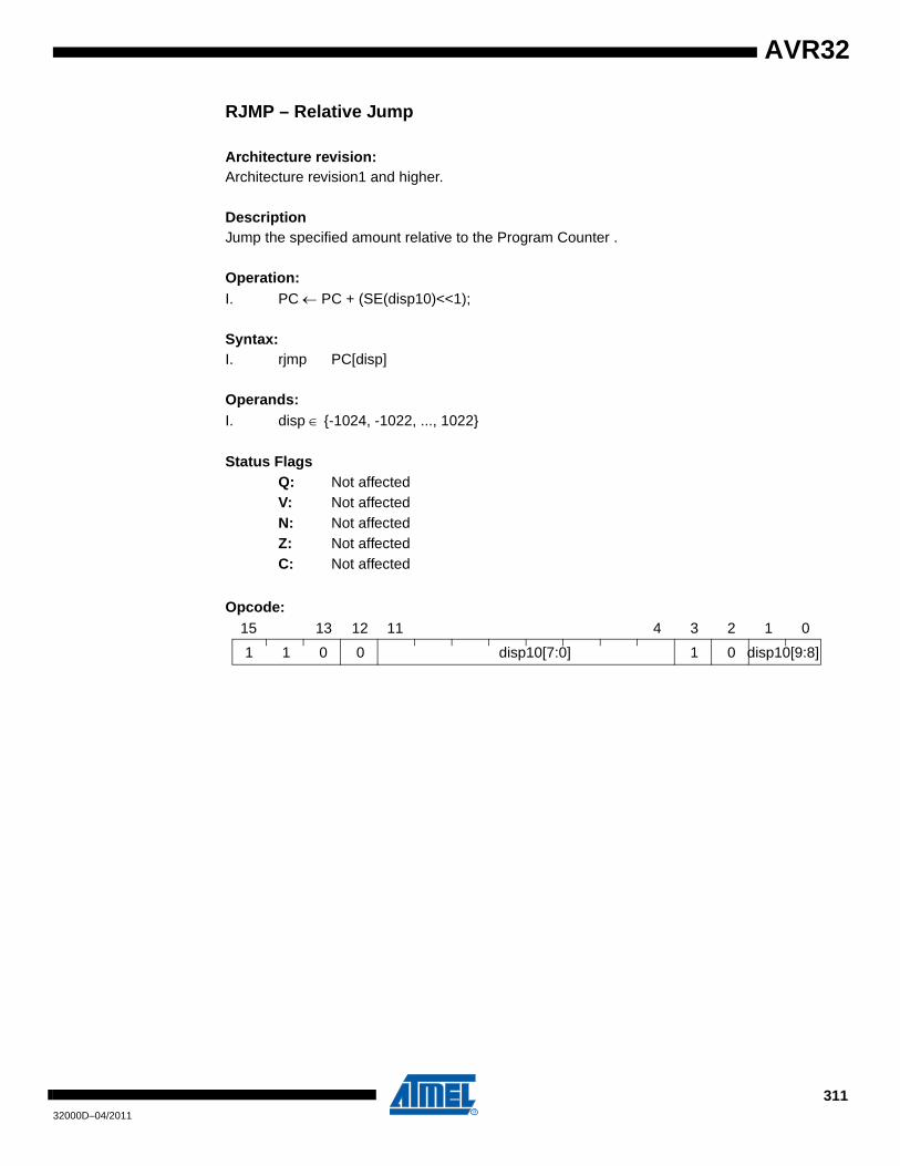
AVR32
RJMP – Relative Jump
Architecture revision:Architecture revision1 and higher.
DescriptionJump the specified amount relative to the Program Counter .
Operation:I. PC ← PC + (SE(disp10)<<1);
Syntax:I. rjmp PC[disp]
Operands:I. disp ∈ {-1024, -1022, ..., 1022}
Status FlagsQ: Not affectedV: Not affectedN: Not affectedZ: Not affectedC: Not affected
Opcode:
1 1 0 0 disp10[7:0] 1 0 disp10[9:8]
15 13 12 11 4 3 2 1 0
31132000D–04/2011

ROL – Rotate Left through Carry
Architecture revision:Architecture revision1 and higher.
DescriptionShift all bits in Rd one place to the left. The C flag is shifted into the LSB. The MSB is shifted into the C flag.
Operation:I. C´ ← Rd[31];
Rd ← Rd << 1;Rd[0] ← C;C ← C´;
Syntax:I. rol Rd
Operands:I. d ∈ {0, 1, …, 15}
Status Flags:Q: Not affectedV: Not affectedN: N ← Res[31]Z: Z ← (RES[31:0] == 0)C: C ← Rd[31]
Opcode:
0 1 0 1 1 1 0 0 1 1 1 1 Rd
15 13 12 9 8 4 3 0
31232000D–04/2011
AVR32

AVR32
ROR – Rotate Right through Carry
Architecture revision:Architecture revision1 and higher.
DescriptionShift all bits in Rd one place to the right. The C flag is shifted into the MSB. The LSB is shifted into the C flag.
Operation:I. C´ ← Rd[0];
Rd ← Rd >> 1;Rd[31] ← C;C ← C´;
Syntax:I. ror Rd
Operands:I. d ∈ {0, 1, …, 15}
Status Flags:Q: Not affectedV: Not affectedN: N ← Res[31]Z: Z ← (RES[31:0] == 0)C: C ← Rd[0]
Opcode:
0 1 0 1 1 1 0 1 0 0 0 0 Rd
15 13 12 9 8 4 3 0
31332000D–04/2011
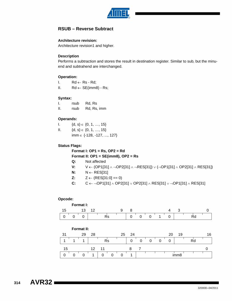
RSUB – Reverse Subtract
Architecture revision:Architecture revision1 and higher.
DescriptionPerforms a subtraction and stores the result in destination register. Similar to sub, but the minu-end and subtrahend are interchanged.
Operation:I. Rd ← Rs - Rd;II. Rd ← SE(imm8) - Rs;
Syntax:I. rsub Rd, RsII. rsub Rd, Rs, imm
Operands:I. {d, s} ∈ {0, 1, …, 15}II. {d, s} ∈ {0, 1, …, 15}
imm ∈ {-128, -127, ..., 127}
Status Flags:Format I: OP1 = Rs, OP2 = RdFormat II: OP1 = SE(imm8), OP2 = RsQ: Not affectedV: V ← (OP1[31] ∧ ¬OP2[31] ∧ ¬RES[31]) ∨ (¬OP1[31] ∧ OP2[31] ∧ RES[31])N: N ← RES[31]Z: Z ← (RES[31:0] == 0)C: C ← ¬OP1[31] ∧ OP2[31] ∨ OP2[31] ∧ RES[31] ∨ ¬OP1[31] ∧ RES[31]
Opcode:
Format I:
Format II:
0 0 0 Rs 0 0 0 1 0 Rd
15 13 12 9 8 4 3 0
1 1 1 Rs 0 0 0 0 0 Rd
31 29 28 25 24 20 19 16
0 0 0 1 0 0 0 1 imm8
15 12 11 8 7 0
31432000D–04/2011
AVR32
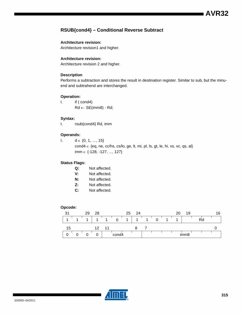
AVR32
RSUB{cond4} – Conditional Reverse Subtract
Architecture revision:Architecture revision1 and higher.
Architecture revision: Architecture revision 2 and higher.
DescriptionPerforms a subtraction and stores the result in destination register. Similar to sub, but the minu-end and subtrahend are interchanged.
Operation:I. if ( cond4)
Rd ← SE(imm8) - Rd;
Syntax:I. rsub{cond4} Rd, imm
Operands:I. d ∈ {0, 1, …, 15}
cond4 ∈ {eq, ne, cc/hs, cs/lo, ge, lt, mi, pl, ls, gt, le, hi, vs, vc, qs, al}imm ∈ {-128, -127, ..., 127}
Status Flags:Q: Not affected.V: Not affected.N: Not affected.Z: Not affected.C: Not affected.
Opcode:
1 1 1 1 0 1 1 1 0 1 1 Rd
31 29 28 25 24 20 19 16
0 0 0 0 cond4 imm8
15 12 11 8 7 0
1
31532000D–04/2011
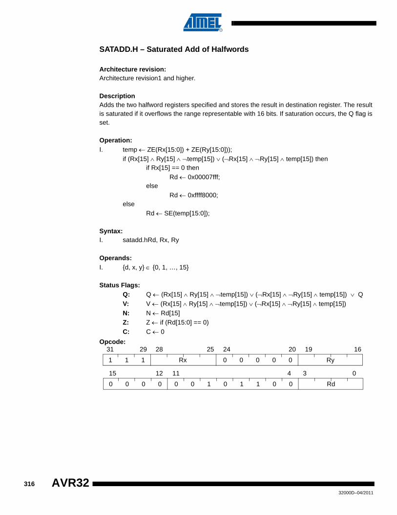
SATADD.H – Saturated Add of Halfwords
Architecture revision:Architecture revision1 and higher.
DescriptionAdds the two halfword registers specified and stores the result in destination register. The result is saturated if it overflows the range representable with 16 bits. If saturation occurs, the Q flag is set.
Operation:I. temp ← ZE(Rx[15:0]) + ZE(Ry[15:0]));
if (Rx[15] ∧ Ry[15] ∧ ¬temp[15]) ∨ (¬Rx[15] ∧ ¬Ry[15] ∧ temp[15]) thenif Rx[15] == 0 then
Rd ← 0x00007fff;else
Rd ← 0xffff8000;else
Rd ← SE(temp[15:0]);
Syntax:I. satadd.hRd, Rx, Ry
Operands:I. {d, x, y} ∈ {0, 1, …, 15}
Status Flags:Q: Q ← (Rx[15] ∧ Ry[15] ∧ ¬temp[15]) ∨ (¬Rx[15] ∧ ¬Ry[15] ∧ temp[15]) ∨ QV: V ← (Rx[15] ∧ Ry[15] ∧ ¬temp[15]) ∨ (¬Rx[15] ∧ ¬Ry[15] ∧ temp[15]) N: N ← Rd[15] Z: Z ← if (Rd[15:0] == 0)C: C ← 0
Opcode:
1 1 1 Rx 0 0 0 0 0 Ry
31 29 28 25 24 20 19 16
0 0 0 0 0 0 1 0 1 1 0 0 Rd
15 12 11 4 3 0
31632000D–04/2011
AVR32
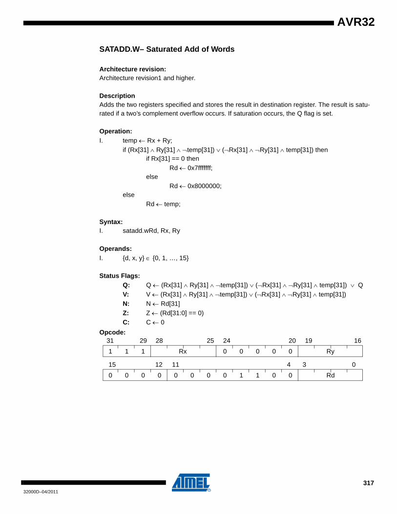
AVR32
SATADD.W– Saturated Add of Words
Architecture revision:Architecture revision1 and higher.
DescriptionAdds the two registers specified and stores the result in destination register. The result is satu-rated if a two’s complement overflow occurs. If saturation occurs, the Q flag is set.
Operation:I. temp ← Rx + Ry;
if (Rx[31] ∧ Ry[31] ∧ ¬temp[31]) ∨ (¬Rx[31] ∧ ¬Ry[31] ∧ temp[31]) thenif Rx[31] == 0 then
Rd ← 0x7fffffff;else
Rd ← 0x8000000;else
Rd ← temp;
Syntax:I. satadd.wRd, Rx, Ry
Operands:I. {d, x, y} ∈ {0, 1, …, 15}
Status Flags:Q: Q ← (Rx[31] ∧ Ry[31] ∧ ¬temp[31]) ∨ (¬Rx[31] ∧ ¬Ry[31] ∧ temp[31]) ∨ QV: V ← (Rx[31] ∧ Ry[31] ∧ ¬temp[31]) ∨ (¬Rx[31] ∧ ¬Ry[31] ∧ temp[31])N: N ← Rd[31] Z: Z ← (Rd[31:0] == 0)C: C ← 0
Opcode:
1 1 1 Rx 0 0 0 0 0 Ry
31 29 28 25 24 20 19 16
0 0 0 0 0 0 0 0 1 1 0 0 Rd
15 12 11 4 3 0
31732000D–04/2011
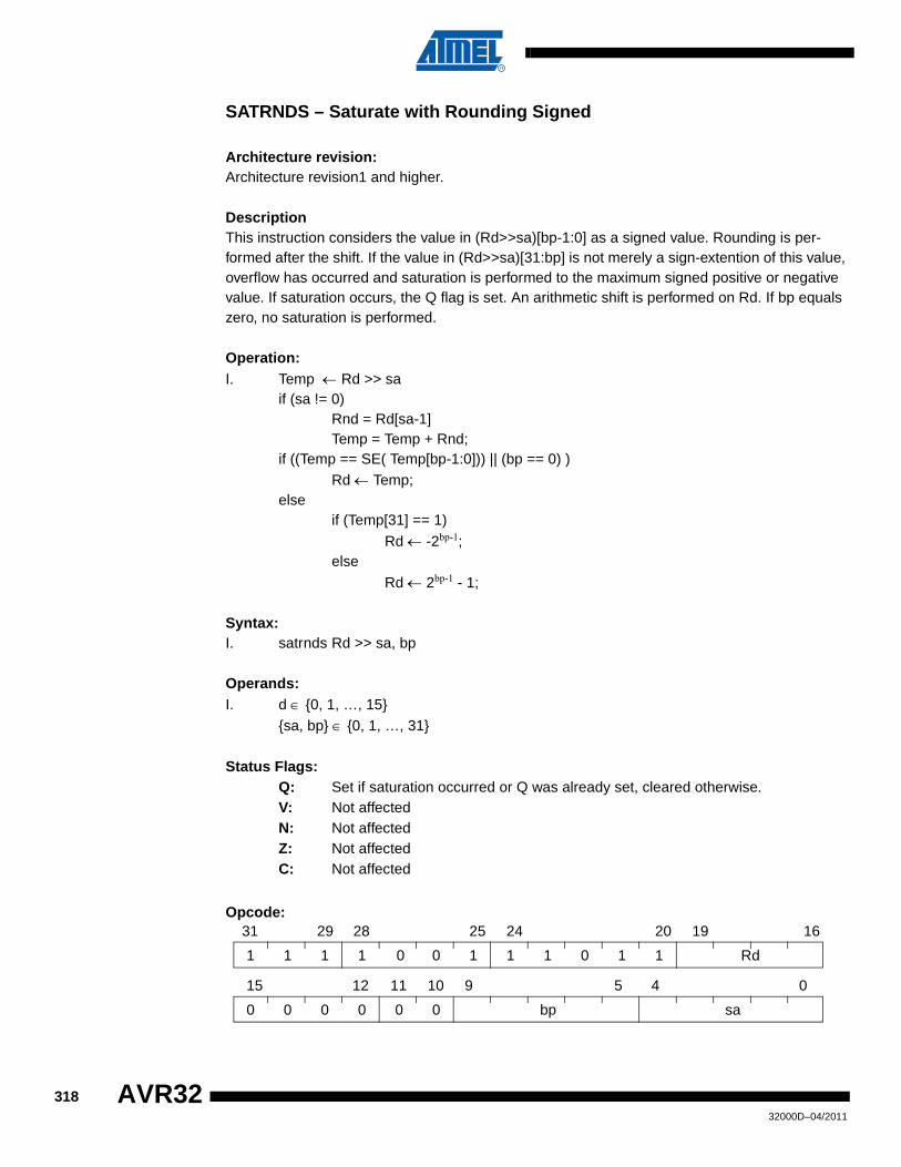
SATRNDS – Saturate with Rounding Signed
Architecture revision:Architecture revision1 and higher.
DescriptionThis instruction considers the value in (Rd>>sa)[bp-1:0] as a signed value. Rounding is per-formed after the shift. If the value in (Rd>>sa)[31:bp] is not merely a sign-extention of this value, overflow has occurred and saturation is performed to the maximum signed positive or negative value. If saturation occurs, the Q flag is set. An arithmetic shift is performed on Rd. If bp equals zero, no saturation is performed.
Operation:I. Temp ← Rd >> sa
if (sa != 0)Rnd = Rd[sa-1]Temp = Temp + Rnd;
if ((Temp == SE( Temp[bp-1:0])) || (bp == 0) )Rd ← Temp;
elseif (Temp[31] == 1)
Rd ← -2bp-1;else
Rd ← 2bp-1 - 1;
Syntax:I. satrnds Rd >> sa, bp
Operands:I. d ∈ {0, 1, …, 15}
{sa, bp} ∈ {0, 1, …, 31}
Status Flags:Q: Set if saturation occurred or Q was already set, cleared otherwise.V: Not affectedN: Not affectedZ: Not affectedC: Not affected
Opcode:
1 1 1 1 0 1 1 1 0 1 1 Rd
31 29 28 25 24 20 19 16
0 0 0 0 0 0 bp sa
15 12 11 10 9 5 4 0
0
31832000D–04/2011
AVR32

AVR32
SATRNDU – Saturate with Rounding Unsigned
Architecture revision:Architecture revision1 and higher.
DescriptionThis instruction considers the value in (Rd>>sa)[bp-1:0] as a unsigned value. Rounding is per-formed after the shift. If the value in (Rd>>sa)[31:bp] is not merely a zero extention of this value, overflow has occurred and saturation is performed to the maximum unsigned positive value or zero. If saturation occurs, the Q flag is set. An arithmetic shift is performed on Rd. If bp equals zero, no saturation is performed.
Operation:
I. Temp ← Rd >> saif (sa != 0)
Rnd = Rd[sa-1]Temp = Temp + Rnd;
If ((Temp == ZE( Temp[bp-1:0])) || (bp == 0) )Rd ← Temp;
elseif (Temp[31] == 1)
Rd ← 0x0000_0000;else
Rd ← 2bp - 1;
Syntax:I. satrndu Rd >> sa, bp
Operands:I. d ∈ {0, 1, …, 15}
{sa, bp} ∈ {0, 1, …, 31}
Status Flags:Q: Set if saturation occurred or Q was already set, cleared otherwise.V: Not affectedN: Not affectedZ: Not affectedC: Not affected
Opcode:
1 1 1 1 0 1 1 1 0 1 1 Rd
31 29 28 25 24 20 19 16
0 0 0 0 0 1 bp sa
15 12 11 10 9 5 4 0
0
31932000D–04/2011
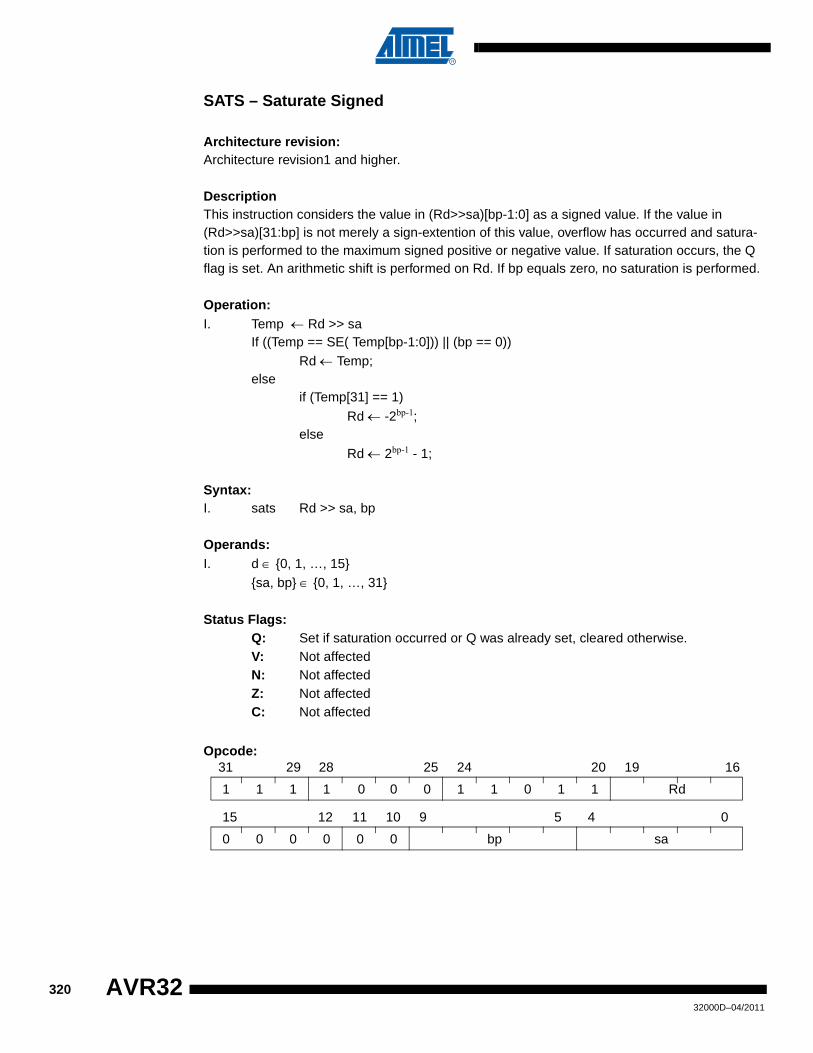
SATS – Saturate Signed
Architecture revision:Architecture revision1 and higher.
DescriptionThis instruction considers the value in (Rd>>sa)[bp-1:0] as a signed value. If the value in (Rd>>sa)[31:bp] is not merely a sign-extention of this value, overflow has occurred and satura-tion is performed to the maximum signed positive or negative value. If saturation occurs, the Q flag is set. An arithmetic shift is performed on Rd. If bp equals zero, no saturation is performed.
Operation:I. Temp ← Rd >> sa
If ((Temp == SE( Temp[bp-1:0])) || (bp == 0))Rd ← Temp;
elseif (Temp[31] == 1)
Rd ← -2bp-1;else
Rd ← 2bp-1 - 1;
Syntax:I. sats Rd >> sa, bp
Operands:I. d ∈ {0, 1, …, 15}
{sa, bp} ∈ {0, 1, …, 31}
Status Flags:Q: Set if saturation occurred or Q was already set, cleared otherwise.V: Not affectedN: Not affectedZ: Not affectedC: Not affected
Opcode:
1 1 1 1 0 0 1 1 0 1 1 Rd
31 29 28 25 24 20 19 16
0 0 0 0 0 0 bp sa
15 12 11 10 9 5 4 0
0
32032000D–04/2011
AVR32
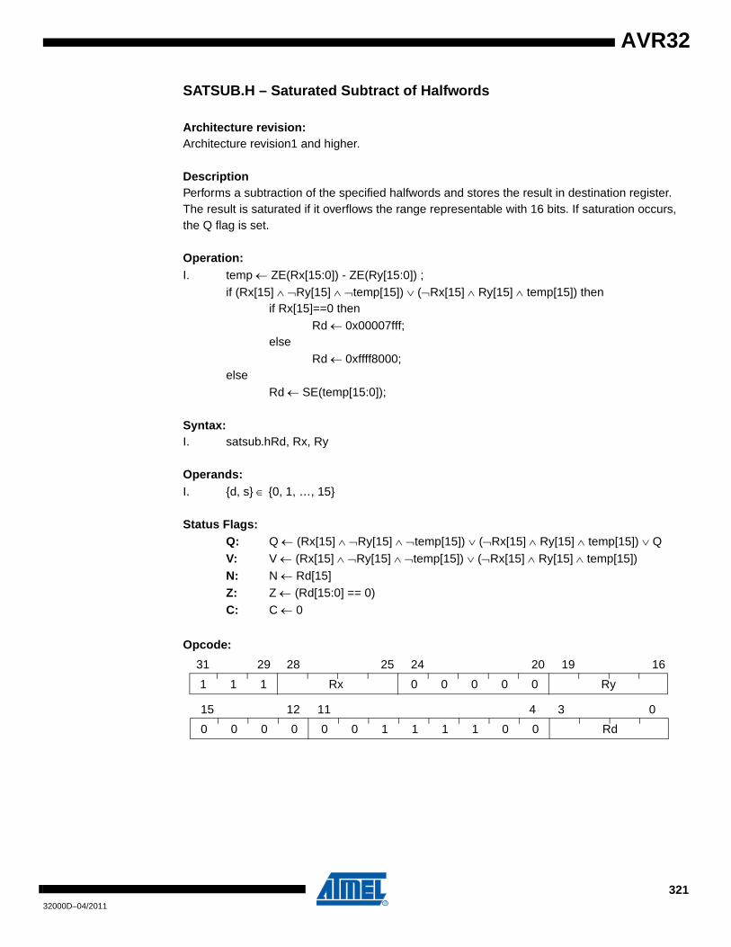
AVR32
SATSUB.H – Saturated Subtract of Halfwords
Architecture revision:Architecture revision1 and higher.
DescriptionPerforms a subtraction of the specified halfwords and stores the result in destination register. The result is saturated if it overflows the range representable with 16 bits. If saturation occurs, the Q flag is set.
Operation:I. temp ← ZE(Rx[15:0]) - ZE(Ry[15:0]) ;
if (Rx[15] ∧ ¬Ry[15] ∧ ¬temp[15]) ∨ (¬Rx[15] ∧ Ry[15] ∧ temp[15]) thenif Rx[15]==0 then
Rd ← 0x00007fff;else
Rd ← 0xffff8000;else
Rd ← SE(temp[15:0]);
Syntax:I. satsub.hRd, Rx, Ry
Operands:I. {d, s} ∈ {0, 1, …, 15}
Status Flags:Q: Q ← (Rx[15] ∧ ¬Ry[15] ∧ ¬temp[15]) ∨ (¬Rx[15] ∧ Ry[15] ∧ temp[15]) ∨ QV: V ← (Rx[15] ∧ ¬Ry[15] ∧ ¬temp[15]) ∨ (¬Rx[15] ∧ Ry[15] ∧ temp[15])N: N ← Rd[15]Z: Z ← (Rd[15:0] == 0)C: C ← 0
Opcode:
1 1 1 Rx 0 0 0 0 0 Ry
31 29 28 25 24 20 19 16
0 0 0 0 0 0 1 1 1 1 0 0 Rd
15 12 11 4 3 0
32132000D–04/2011
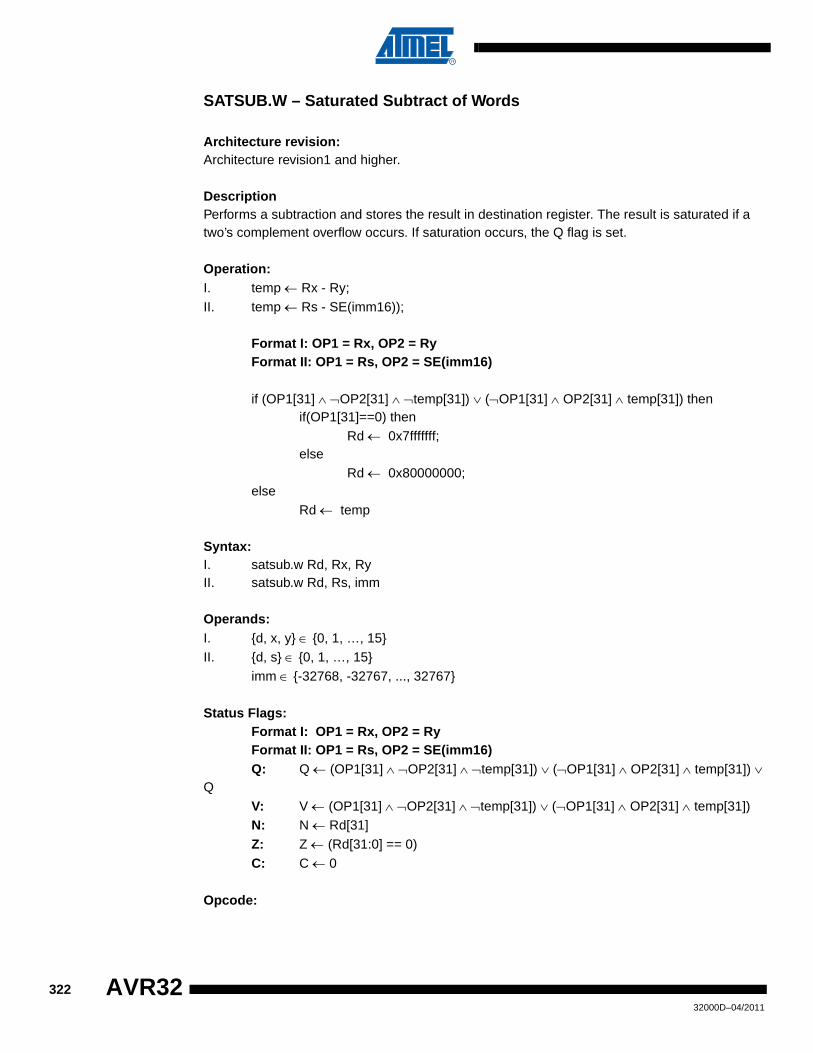
SATSUB.W – Saturated Subtract of Words
Architecture revision:Architecture revision1 and higher.
DescriptionPerforms a subtraction and stores the result in destination register. The result is saturated if a two’s complement overflow occurs. If saturation occurs, the Q flag is set.
Operation:I. temp ← Rx - Ry;II. temp ← Rs - SE(imm16));
Format I: OP1 = Rx, OP2 = RyFormat II: OP1 = Rs, OP2 = SE(imm16)
if (OP1[31] ∧ ¬OP2[31] ∧ ¬temp[31]) ∨ (¬OP1[31] ∧ OP2[31] ∧ temp[31]) thenif(OP1[31]==0) then
Rd ← 0x7fffffff;else
Rd ← 0x80000000;else
Rd ← temp
Syntax:I. satsub.w Rd, Rx, RyII. satsub.w Rd, Rs, imm
Operands:I. {d, x, y} ∈ {0, 1, …, 15}II. {d, s} ∈ {0, 1, …, 15}
imm ∈ {-32768, -32767, ..., 32767}
Status Flags:Format I: OP1 = Rx, OP2 = RyFormat II: OP1 = Rs, OP2 = SE(imm16)Q: Q ← (OP1[31] ∧ ¬OP2[31] ∧ ¬temp[31]) ∨ (¬OP1[31] ∧ OP2[31] ∧ temp[31]) ∨
QV: V ← (OP1[31] ∧ ¬OP2[31] ∧ ¬temp[31]) ∨ (¬OP1[31] ∧ OP2[31] ∧ temp[31])N: N ← Rd[31]Z: Z ← (Rd[31:0] == 0)C: C ← 0
Opcode:
32232000D–04/2011
AVR32
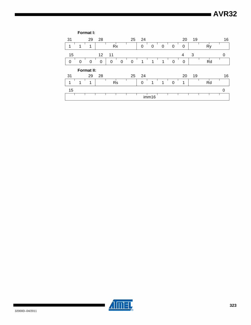
AVR32
Format I:
Format II:
1 1 1 Rx 0 0 0 0 0 Ry
31 29 28 25 24 20 19 16
0 0 0 0 0 0 0 1 1 1 0 0 Rd
15 12 11 4 3 0
1 1 1 Rs 0 1 1 0 1 Rd
31 29 28 25 24 20 19 16
imm16
15 0
32332000D–04/2011
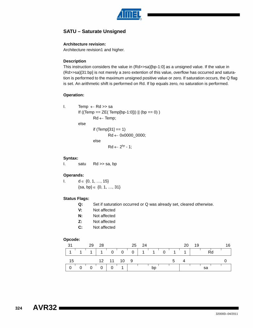
SATU – Saturate Unsigned
Architecture revision:Architecture revision1 and higher.
DescriptionThis instruction considers the value in (Rd>>sa)[bp-1:0] as a unsigned value. If the value in (Rd>>sa)[31:bp] is not merely a zero extention of this value, overflow has occurred and satura-tion is performed to the maximum unsigned positive value or zero. If saturation occurs, the Q flag is set. An arithmetic shift is performed on Rd. If bp equals zero, no saturation is performed.
Operation:
I. Temp ← Rd >> saIf ((Temp == ZE( Temp[bp-1:0])) || (bp == 0) )
Rd ← Temp;else
if (Temp[31] == 1)Rd ← 0x0000_0000;
else
Rd ← 2bp - 1;
Syntax:I. satu Rd >> sa, bp
Operands:I. d ∈ {0, 1, …, 15}
{sa, bp} ∈ {0, 1, …, 31}
Status Flags:Q: Set if saturation occurred or Q was already set, cleared otherwise.V: Not affectedN: Not affectedZ: Not affectedC: Not affected
Opcode:
1 1 1 1 0 0 1 1 0 1 1 Rd
31 29 28 25 24 20 19 16
0 0 0 0 0 1 bp sa
15 12 11 10 9 5 4 0
0
32432000D–04/2011
AVR32

AVR32
SBC – Subtract with Carry
Architecture revision:Architecture revision1 and higher.
DescriptionSubtracts a specified register and the value of the carry bit from a destination register and stores the result in the destination register.
Operation:I. Rd ← Rx - Ry - C;
Syntax:I. sbc Rd, Rx, Ry
Operands:I. {x, y, d} ∈ {0, 1, …, 15}
Status Flags:Q: Not affected.V: V ← (Rx[31] ∧ ¬Ry[31] ∧ ¬RES[31]) ∨ (¬Rx[31] ∧ Ry[31] ∧ RES[31])N: N ← RES[31]Z: Z ← (RES[31:0] == 0) ∧ ZC: C ← ¬Rx[31] ∧ Ry[31] ∨ Ry[31] ∧ RES[31] ∨ ¬Rx[31] ∧ RES[31]
Opcode:
1 1 1 Rx 0 0 0 0 0 Ry
31 29 28 25 24 20 19 16
0 0 0 0 0 0 0 1 0 1 0 0 Rd
15 12 11 4 3 0
32532000D–04/2011

SBR – Set Bit in Register
Architecture revision:Architecture revision1 and higher.
DescriptionSets a bit in the specified register. All other bits are unaffected.
Operation:I. Rd[bp5] ← 1;
Syntax:I. sbr Rd, bp
Operands:I. d ∈ {0, 1, …, 15}
bp ∈ {0, 1, …, 31}
Status Flags:Q: Not affectedV: Not affectedN: Not affectedZ: Z ← 0C: Not affected
Opcode:
1 0 1 bp[4:1] 1 1 0 1 bp[0] Rd
15 13 12 9 8 5 4 3 0
32632000D–04/2011
AVR32
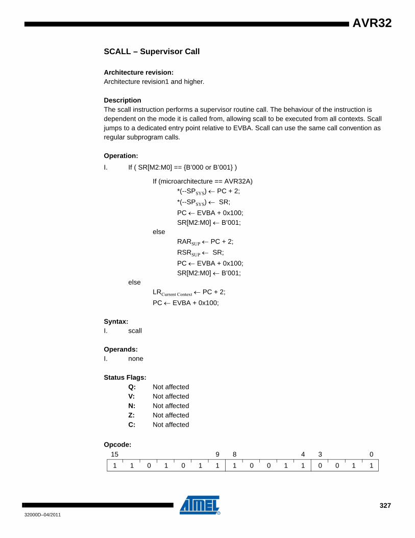
AVR32
SCALL – Supervisor Call
Architecture revision:Architecture revision1 and higher.
DescriptionThe scall instruction performs a supervisor routine call. The behaviour of the instruction is dependent on the mode it is called from, allowing scall to be executed from all contexts. Scall jumps to a dedicated entry point relative to EVBA. Scall can use the same call convention as regular subprogram calls.
Operation:
I. If ( SR[M2:M0] == {B’000 or B’001} )
If (microarchitecture == AVR32A)*(--SPSYS) ← PC + 2;
*(--SPSYS) ← SR;
PC ← EVBA + 0x100;SR[M2:M0] ← B’001;
elseRARSUP ← PC + 2;
RSRSUP ← SR;
PC ← EVBA + 0x100;SR[M2:M0] ← B’001;
else LRCurrent Context ← PC + 2;
PC ← EVBA + 0x100;
Syntax:I. scall
Operands:I. none
Status Flags:Q: Not affectedV: Not affectedN: Not affectedZ: Not affectedC: Not affected
Opcode:
1 1 0 1 0 1 1 1 0 0 1 1 0 0 1 1
15 9 8 4 3 0
32732000D–04/2011
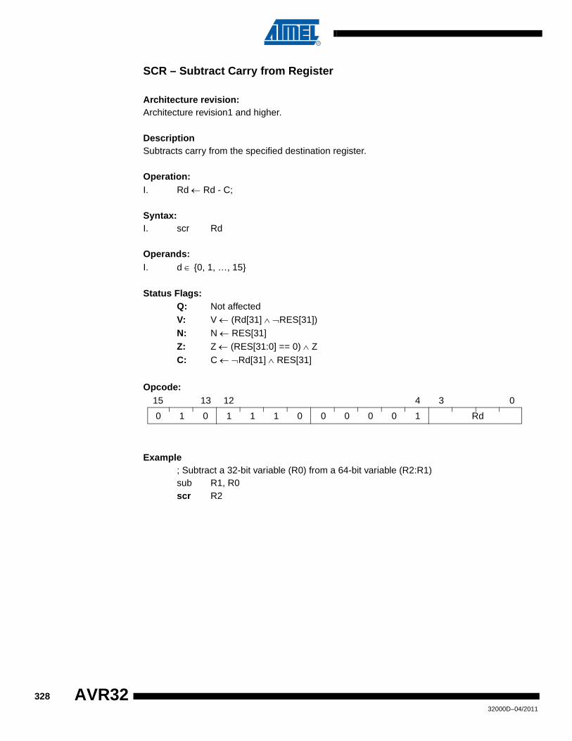
SCR – Subtract Carry from Register
Architecture revision:Architecture revision1 and higher.
DescriptionSubtracts carry from the specified destination register.
Operation:I. Rd ← Rd - C;
Syntax:I. scr Rd
Operands: I. d ∈ {0, 1, …, 15}
Status Flags:Q: Not affectedV: V ← (Rd[31] ∧ ¬RES[31])N: N ← RES[31]Z: Z ← (RES[31:0] == 0) ∧ ZC: C ← ¬Rd[31] ∧ RES[31]
Opcode:
Example; Subtract a 32-bit variable (R0) from a 64-bit variable (R2:R1)sub R1, R0scr R2
0 1 0 1 1 1 0 0 0 0 0 1 Rd
15 13 12 4 3 0
32832000D–04/2011
AVR32

AVR32
SLEEP – Set CPU Activity Mode
Architecture revision:Architecture revision1 and higher.
DescriptionSets the system in the sleep mode specified by the implementation defined Op8 operand. The semantic of Op8 is IMPLEMENTATION DEFINED. If bit 7 in Op8 is one, SR[GM] will be cleared when entering sleep mode.
Operation:I. Set the system in the specified sleep mode.
Syntax:I. sleep Op8
Operands:I. Op8 ∈ {0, 1, …, 255}
Status Flags:Q: Not affectedV: Not affectedN: Not affectedZ: Not affectedC: Not affected
Opcode:
Note:The sleep instruction is a privileged instruction, and will trigger a Privilege Violation exception if executed in user mode.
1 1 1 0 0 0 1 1 0 1 1 0 0 0
31 29 28 25 24 20 19 16
0 0 0 0 0 0 0 0 Op8
15 8 7 0
1 0
32932000D–04/2011
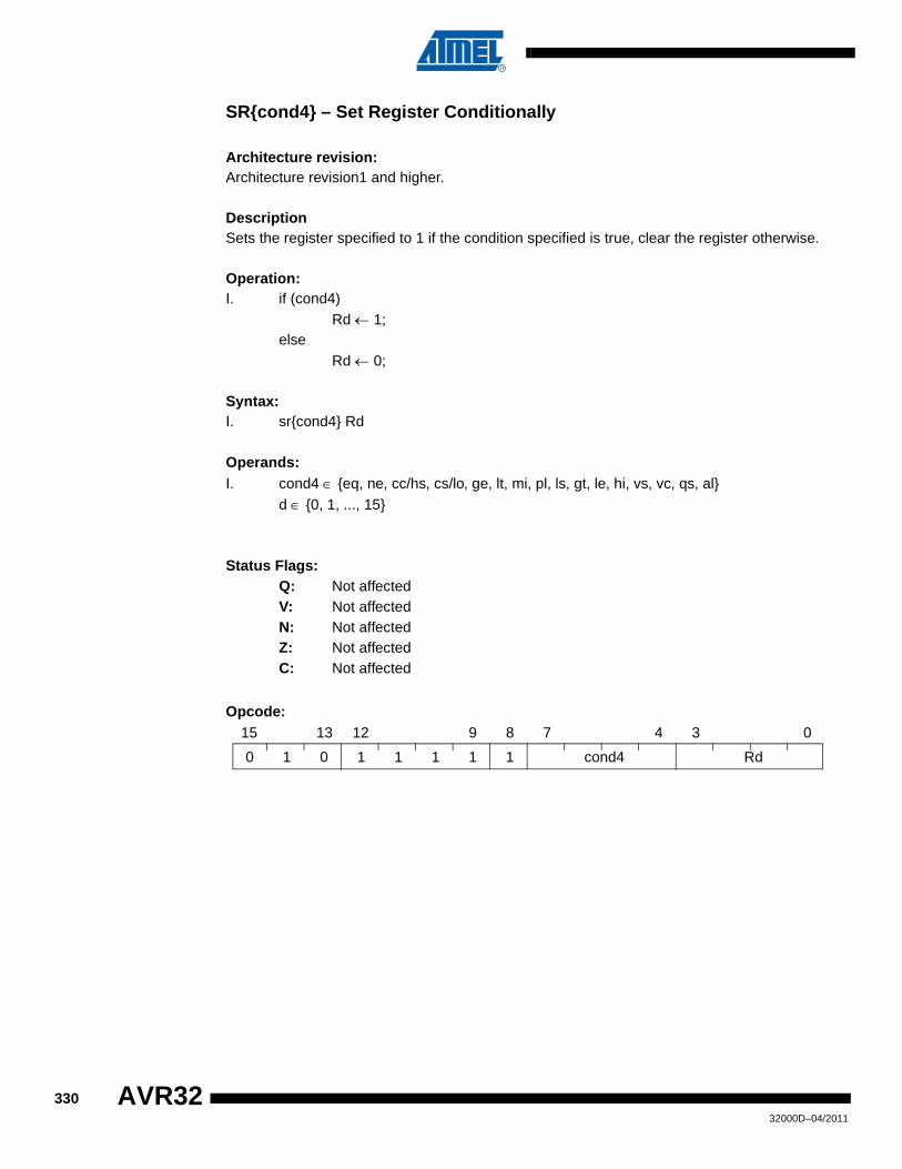
SR{cond4} – Set Register Conditionally
Architecture revision:Architecture revision1 and higher.
DescriptionSets the register specified to 1 if the condition specified is true, clear the register otherwise.
Operation:I. if (cond4)
Rd ← 1;else
Rd ← 0;
Syntax:I. sr{cond4} Rd
Operands:I. cond4 ∈ {eq, ne, cc/hs, cs/lo, ge, lt, mi, pl, ls, gt, le, hi, vs, vc, qs, al}
d ∈ {0, 1, ..., 15}
Status Flags:Q: Not affectedV: Not affectedN: Not affectedZ: Not affectedC: Not affected
Opcode:
0 1 0 1 1 1 1 1 cond4 Rd
15 13 12 9 8 7 4 3 0
33032000D–04/2011
AVR32
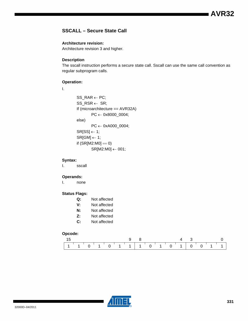
AVR32
SSCALL – Secure State Call
Architecture revision:Architecture revision 3 and higher.
DescriptionThe sscall instruction performs a secure state call. Sscall can use the same call convention as regular subprogram calls.
Operation:
I.
SS_RAR ← PC;SS_RSR ← SR;If (microarchitecture == AVR32A)
PC ← 0x8000_0004;else)
PC ← 0xA000_0004;SR[SS] ← 1;SR[GM] ← 1;if (SR[M2:M0] == 0)
SR[M2:M0] ← 001;
Syntax:I. sscall
Operands:I. none
Status Flags:Q: Not affectedV: Not affectedN: Not affectedZ: Not affectedC: Not affected
Opcode:
1 1 0 1 0 1 1 1 0 1 0 1 0 0 1 1
15 9 8 4 3 0
33132000D–04/2011
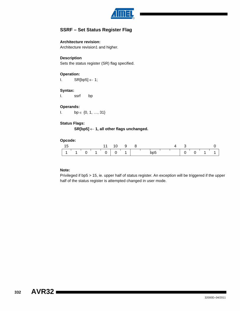
SSRF – Set Status Register Flag
Architecture revision:Architecture revision1 and higher.
DescriptionSets the status register (SR) flag specified.
Operation:I. SR[bp5] ← 1;
Syntax:I. ssrf bp
Operands:I. bp ∈ {0, 1, …, 31}
Status Flags:SR[bp5] ← 1, all other flags unchanged.
Opcode:
Note:Privileged if bp5 > 15, ie. upper half of status register. An exception will be triggered if the upper half of the status register is attempted changed in user mode.
1 1 0 1 0 0 1 bp5 0 0 1 1
15 11 10 9 8 4 3 0
33232000D–04/2011
AVR32
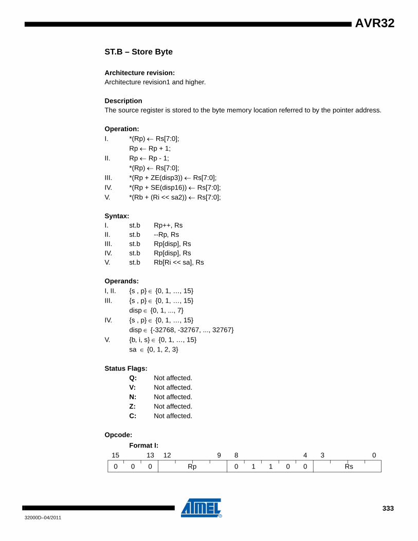
AVR32
ST.B – Store Byte
Architecture revision:Architecture revision1 and higher.
DescriptionThe source register is stored to the byte memory location referred to by the pointer address.
Operation:I. *(Rp) ← Rs[7:0];
Rp ← Rp + 1;II. Rp ← Rp - 1;
*(Rp) ← Rs[7:0];III. *(Rp + ZE(disp3)) ← Rs[7:0];IV. *(Rp + SE(disp16)) ← Rs[7:0];V. *(Rb + (Ri << sa2)) ← Rs[7:0];
Syntax:I. st.b Rp++, RsII. st.b --Rp, RsIII. st.b Rp[disp], RsIV. st.b Rp[disp], RsV. st.b Rb[Ri << sa], Rs
Operands:I, II. {s , p} ∈ {0, 1, …, 15}III. {s , p} ∈ {0, 1, …, 15}
disp ∈ {0, 1, ..., 7}IV. {s , p} ∈ {0, 1, …, 15}
disp ∈ {-32768, -32767, ..., 32767}V. {b, i, s} ∈ {0, 1, …, 15}
sa ∈ {0, 1, 2, 3}
Status Flags:Q: Not affected.V: Not affected.N: Not affected.Z: Not affected.C: Not affected.
Opcode:
Format I:
0 0 0 Rp 0 1 1 0 0 Rs
15 13 12 9 8 4 3 0
33332000D–04/2011
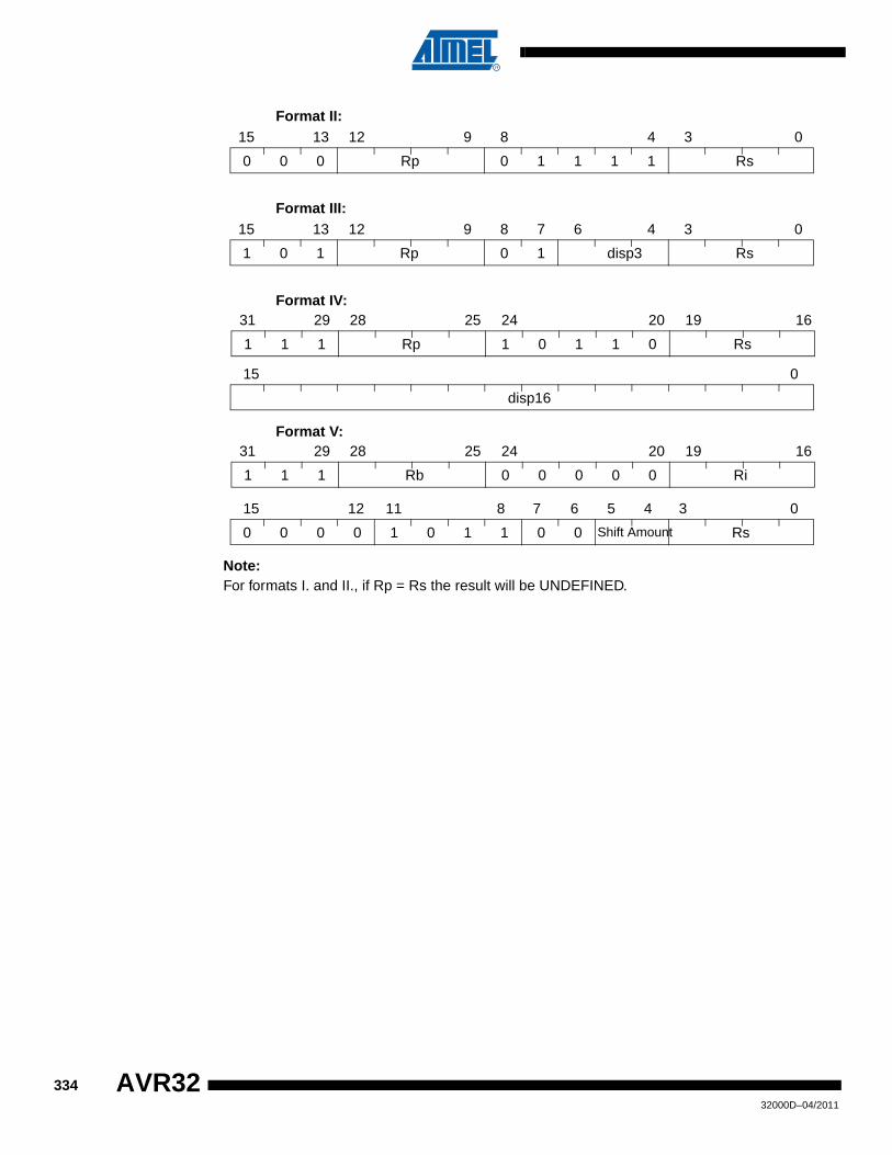
Format II:
Format III:
Format IV:
Format V:
Note:For formats I. and II., if Rp = Rs the result will be UNDEFINED.
0 0 0 Rp 0 1 1 1 1 Rs
15 13 12 9 8 4 3 0
1 0 1 Rp 0 1 disp3 Rs
15 13 12 9 8 7 6 4 3 0
1 1 1 Rp 1 0 1 1 0 Rs
31 29 28 25 24 20 19 16
disp16
15 0
1 1 1 Rb 0 0 0 0 0 Ri
31 29 28 25 24 20 19 16
0 0 0 0 1 0 1 1 0 0 Shift Amount Rs
15 12 11 8 7 6 5 4 3 0
33432000D–04/2011
AVR32

AVR32
ST.B{cond4} – Conditionally Store Byte
Architecture revision: Architecture revision 2 and higher.
DescriptionThe source register is stored to the byte memory location referred to by the pointer address if the given condition is satisfied.
Operation:I. if (cond4)
*(Rp + ZE(disp9)) ← Rs[7:0];
Syntax:I. st.b{cond4} Rp[disp], Rs
Operands:I. s, p ∈ {0, 1, …, 15}
disp ∈ {0, 1, ..., 511}cond4 ∈ {eq, ne, cc/hs, cs/lo, ge, lt, mi, pl, ls, gt, le, hi, vs, vc, qs, al}
Status Flags:Q: Not affected.V: Not affected.N: Not affected.Z: Not affected.C: Not affected.
Opcode:
1 1 1 1 1 1 1 1
31 29 28 25 24 20 19 16
cond4 1 1 1 disp9
15 12 11 8 7 6 5 4 3 0
RdRp
33532000D–04/2011

ST.D – Store Doubleword
Architecture revision:Architecture revision1 and higher.
DescriptionThe source registers are stored to the doubleword memory location referred to by the pointer address.
Operation:I. *(Rp) ← Rs+1:Rs;
Rp ← Rp + 8;II. Rp ← Rp - 8;
*(Rp) ← Rs+1:Rs;III. *(Rp) ← Rs+1:Rs;IV. *(Rp + SE(disp16)) ← Rs+1:Rs;V. *(Rb + (Ri << sa2)) ← Rs+1:Rs;
Syntax:I. st.d Rp++, RsII. st.d --Rp, RsIII. st.d Rp, RsIV. st.d Rp[disp], RsV. st.d Rb[Ri << sa], Rs
Operands:I, II, III. p ∈ {0, 1, …, 15}
s ∈ {0, 2, …, 14}IV. p ∈ {0, 1, …, 15}
s ∈ {0, 2, …, 14}disp ∈ {-32768, -32767, ..., 32767}
V. {b, i} ∈ {0, 1, …, 15}s ∈ {0, 2, …, 14}sa ∈ {0, 1, 2, 3}
Status Flags:Q: Not affected.V: Not affected.N: Not affected.Z: Not affected.C: Not affected.
Opcode:
33632000D–04/2011
AVR32

AVR32
Format I:
Format II:
Format III:
Format IV:
Format V:
Note:For formats I. and II., if Rp == Rs the result will be UNDEFINED.
1 0 1 Rp 1 0 0 1 0 Rs 0
15 13 12 9 8 6 5 4 3 1 0
1 0 1 Rp 1 0 0 1 0 Rs 1
15 13 12 9 8 6 5 4 3 1 0
1 0 1 Rp 1 0 0 0 1 Rs 1
15 13 12 9 8 4 3 0
1 1 1 Rp 0 1 1 1 0 Rs 1
31 29 28 25 24 20 19 17 16
disp16
15 0
1 1 1 Rb 0 0 0 0 0 Ri
31 29 28 25 24 20 19 16
0 0 0 0 1 0 0 0 0 0 Shift Amount Rs
15 12 11 8 7 6 5 4 3 0
33732000D–04/2011
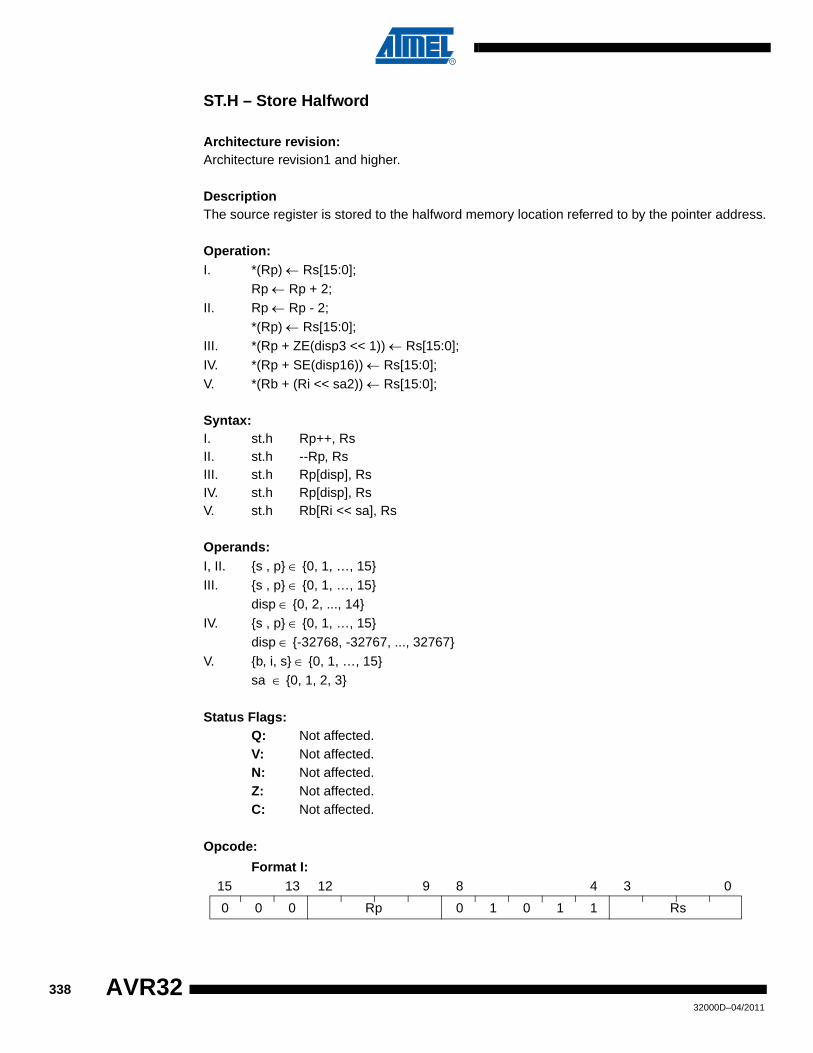
ST.H – Store Halfword
Architecture revision:Architecture revision1 and higher.
DescriptionThe source register is stored to the halfword memory location referred to by the pointer address.
Operation:I. *(Rp) ← Rs[15:0];
Rp ← Rp + 2;II. Rp ← Rp - 2;
*(Rp) ← Rs[15:0];III. *(Rp + ZE(disp3 << 1)) ← Rs[15:0];IV. *(Rp + SE(disp16)) ← Rs[15:0];V. *(Rb + (Ri << sa2)) ← Rs[15:0];
Syntax:I. st.h Rp++, RsII. st.h --Rp, RsIII. st.h Rp[disp], RsIV. st.h Rp[disp], RsV. st.h Rb[Ri << sa], Rs
Operands:I, II. {s , p} ∈ {0, 1, …, 15}III. {s , p} ∈ {0, 1, …, 15}
disp ∈ {0, 2, ..., 14}IV. {s , p} ∈ {0, 1, …, 15}
disp ∈ {-32768, -32767, ..., 32767}V. {b, i, s} ∈ {0, 1, …, 15}
sa ∈ {0, 1, 2, 3}
Status Flags:Q: Not affected.V: Not affected.N: Not affected.Z: Not affected.C: Not affected.
Opcode:
Format I:
0 0 0 Rp 0 1 0 1 1 Rs
15 13 12 9 8 4 3 0
33832000D–04/2011
AVR32
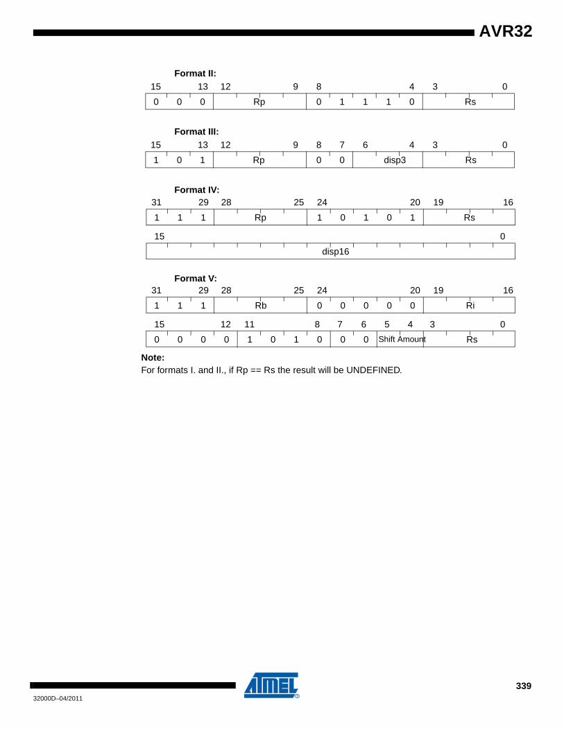
AVR32
Format II:
Format III:
Format IV:
Format V:
Note:For formats I. and II., if Rp == Rs the result will be UNDEFINED.
0 0 0 Rp 0 1 1 1 0 Rs
15 13 12 9 8 4 3 0
1 0 1 Rp 0 0 disp3 Rs
15 13 12 9 8 7 6 4 3 0
1 1 1 Rp 1 0 1 0 1 Rs
31 29 28 25 24 20 19 16
disp16
15 0
1 1 1 Rb 0 0 0 0 0 Ri
31 29 28 25 24 20 19 16
0 0 0 0 1 0 1 0 0 0 Shift Amount Rs
15 12 11 8 7 6 5 4 3 0
33932000D–04/2011

ST.H{cond4} – Conditionally Store Halfword
Architecture revision: Architecture revision 2 and higher.
DescriptionThe source register is stored to the halfword memory location referred to by the pointer address if the given condition is satisfied.
Operation:I. if (cond4)
*(Rp + ZE(disp9<<1)) ← Rs[15:0];
Syntax:I. st.h{cond4} Rp[disp], Rs
Operands:I. s, p ∈ {0, 1, …, 15}
disp ∈ {0, 2, ..., 1022}cond4 ∈ {eq, ne, cc/hs, cs/lo, ge, lt, mi, pl, ls, gt, le, hi, vs, vc, qs, al}
Status Flags:Q: Not affected.V: Not affected.N: Not affected.Z: Not affected.C: Not affected.
Opcode:
1 1 1 1 1 1 1 1
31 29 28 25 24 20 19 16
cond4 1 1 0 disp9
15 12 11 8 7 6 5 4 3 0
RsRp
34032000D–04/2011
AVR32
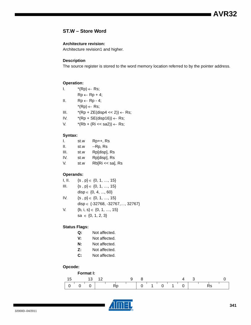
AVR32
ST.W – Store Word
Architecture revision:Architecture revision1 and higher.
DescriptionThe source register is stored to the word memory location referred to by the pointer address.
Operation:I. *(Rp) ← Rs;
Rp ← Rp + 4;II. Rp ← Rp - 4;
*(Rp) ← Rs;III. *(Rp + ZE(disp4 << 2)) ← Rs;IV. *(Rp + SE(disp16)) ← Rs;V. *(Rb + (Ri << sa2)) ← Rs;
Syntax:I. st.w Rp++, RsII. st.w --Rp, RsIII. st.w Rp[disp], RsIV. st.w Rp[disp], RsV. st.w Rb[Ri << sa], Rs
Operands:I, II. {s , p} ∈ {0, 1, …, 15}III. {s , p} ∈ {0, 1, …, 15}
disp ∈ {0, 4, ..., 60}IV. {s , p} ∈ {0, 1, …, 15}
disp ∈ {-32768, -32767,…, 32767}V. {b, i, s} ∈ {0, 1, …, 15}
sa ∈ {0, 1, 2, 3}
Status Flags:Q: Not affected.V: Not affected.N: Not affected.Z: Not affected.C: Not affected.
Opcode:
Format I:
0 0 0 Rp 0 1 0 1 0 Rs
15 13 12 9 8 4 3 0
34132000D–04/2011

Format II:
Format III:
Format IV:
Format V:
Note:For formats I. and II., if Rp == Rs the result will be UNDEFINED.
0 0 0 Rp 0 1 1 0 1 Rs
15 13 12 9 8 4 3 0
1 0 0 Rp 1 disp4 Rs
15 13 12 9 8 7 4 3 0
1 1 1 Rp 1 0 1 0 0 Rs
31 29 28 25 24 20 19 16
disp16
15 0
1 1 1 Rb 0 0 0 0 0 Ri
31 29 28 25 24 20 19 16
0 0 0 0 1 0 0 1 0 0 Shift Amount Rs
15 12 11 8 7 6 5 4 3 0
34232000D–04/2011
AVR32
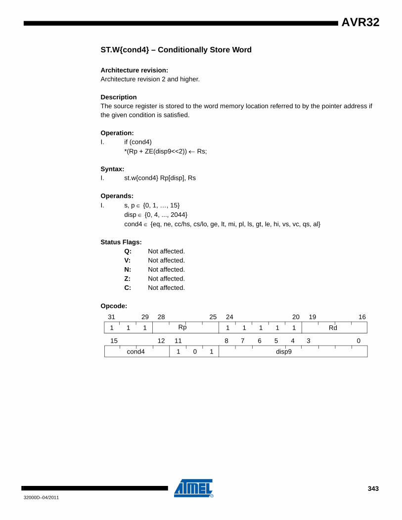
AVR32
ST.W{cond4} – Conditionally Store Word
Architecture revision: Architecture revision 2 and higher.
DescriptionThe source register is stored to the word memory location referred to by the pointer address if the given condition is satisfied.
Operation:I. if (cond4)
*(Rp + ZE(disp9<<2)) ← Rs;
Syntax:I. st.w{cond4} Rp[disp], Rs
Operands:I. s, p ∈ {0, 1, …, 15}
disp ∈ {0, 4, ..., 2044}cond4 ∈ {eq, ne, cc/hs, cs/lo, ge, lt, mi, pl, ls, gt, le, hi, vs, vc, qs, al}
Status Flags:Q: Not affected.V: Not affected.N: Not affected.Z: Not affected.C: Not affected.
Opcode:
1 1 1 1 1 1 1 1
31 29 28 25 24 20 19 16
cond4 1 0 1 disp9
15 12 11 8 7 6 5 4 3 0
RdRp
34332000D–04/2011

STC.{D,W} – Store Coprocessor
Architecture revision:Architecture revision1 and higher.
DescriptionStores the source register value to the location specified by the addressing mode.
Operation:I. *(Rp + (ZE(disp8) << 2)) ← CP#(CRd+1:CRd);II. *(Rp) ← CP#(CRd+1:CRd);
Rp ← Rp+8;III. *(Rb + (Ri << sa2)) ← CP#(CRd+1:CRd);IV. *(Rp + (ZE(disp8) << 2)) ← CP#(CRd);V. *(Rp) ← CP#(CRd);
Rp ← Rp+4;VI. *(Rb + (Ri << sa2)) ← CP#(CRd);
Syntax:I. stc.d CP#, Rp[disp], CRsII. stc.d CP#, Rp++, CRsIII. stc.d CP#, Rb[Ri<<sa], CRsIV. stc.w CP#, Rp[disp], CRsV. stc.w CP#, Rp++, CRsVI. stc.w CP#, Rb[Ri<<sa], CRs
Operands:I-VI. # ∈ {0, 1, …, 7}I-II, IV-V.s ∈ {0, 1, …, 15}I-III. s ∈ {0, 2, …, 14}I, IV. disp ∈ {0, 4, …, 1020}III, VI. {b, i} ∈ {0, 1, …, 15}III, VI. sa ∈ {0, 1, 2, 3}
Status Flags:Q: Not affectedV: Not affectedN: Not affectedZ: Not affectedC: Not affected
Opcode:
34432000D–04/2011
AVR32

AVR32
Format I:
Format II:
Format III:
Format IV:
Format V:
Format VI:
Example:stc.d CP2, R2[0], CR0
1 1 1 0 0 1 1 1 0 1 0 Rp
31 29 28 25 24 20 19 16
CP # 1 CRs[3:1] 0 disp8
15 13 12 11 8 7 0
1
1 1 1 0 1 1 1 1 0 1 0 Rp
31 29 28 25 24 20 19 16
CP # 0 CRs[3:1] 0 0 1 1 1 0 0 0
15 13 12 11 9 8 7 0
1
0
1 1 1 0 1 1 1 1 0 1 0 Rp
31 29 28 25 24 20 19 16
CP # 1 CRs[3:1] 0 1 1 Sh amt Ri
15 13 12 11 9 8 7 6 5 4 3 0
1
1 1 1 0 0 1 1 1 0 1 0 Rp
31 29 28 25 24 20 19 16
CP # 0 CRs disp8
15 13 12 11 8 7 0
1
1 1 1 0 1 1 1 1 0 1 0 Rp
31 29 28 25 24 20 19 16
CP # 0 0 1 1 0 0 0 0
15 13 12 11 8 7 0
1
0CRs
1 1 1 0 1 1 1 1 0 1 0 Rp
31 29 28 25 24 20 19 16
CP # 1 1 0 Sh amt Ri
15 13 12 11 8 7 6 5 4 3 0
1
CRs
34532000D–04/2011
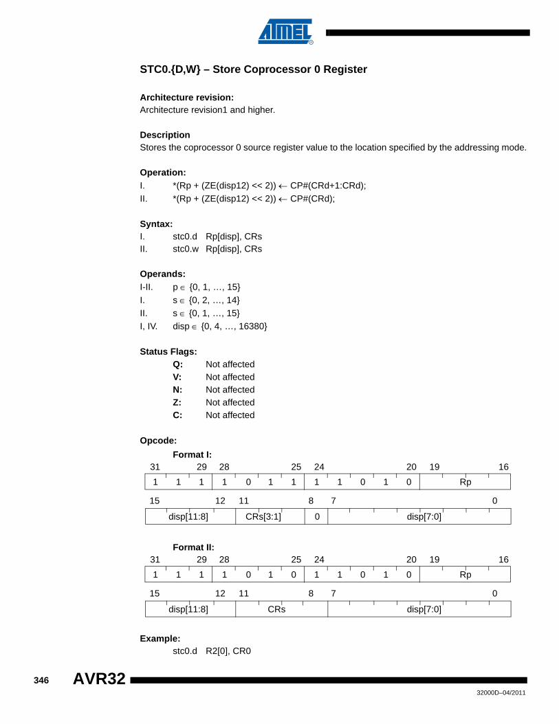
STC0.{D,W} – Store Coprocessor 0 Register
Architecture revision:Architecture revision1 and higher.
DescriptionStores the coprocessor 0 source register value to the location specified by the addressing mode.
Operation:I. *(Rp + (ZE(disp12) << 2)) ← CP#(CRd+1:CRd);II. *(Rp + (ZE(disp12) << 2)) ← CP#(CRd);
Syntax:I. stc0.d Rp[disp], CRsII. stc0.w Rp[disp], CRs
Operands:I-II. p ∈ {0, 1, …, 15}I. s ∈ {0, 2, …, 14}II. s ∈ {0, 1, …, 15}I, IV. disp ∈ {0, 4, …, 16380}
Status Flags:Q: Not affectedV: Not affectedN: Not affectedZ: Not affectedC: Not affected
Opcode:
Format I:
Format II:
Example:stc0.d R2[0], CR0
1 1 1 1 1 1 1 1 0 1 0 Rp
31 29 28 25 24 20 19 16
disp[11:8] CRs[3:1] 0 disp[7:0]
15 12 11 8 7 0
0
1 1 1 1 1 0 1 1 0 1 0 Rp
31 29 28 25 24 20 19 16
disp[11:8] CRs disp[7:0]
15 12 11 8 7 0
0
34632000D–04/2011
AVR32
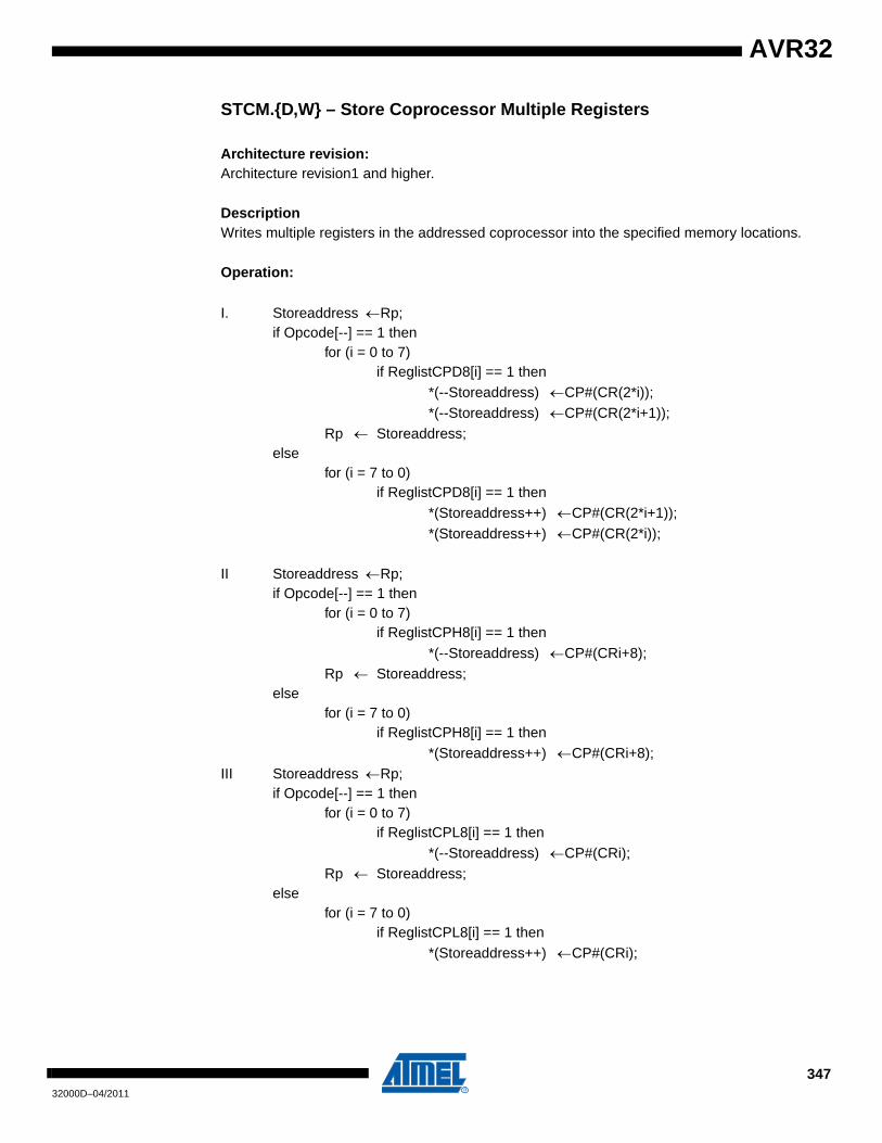
AVR32
STCM.{D,W} – Store Coprocessor Multiple Registers
Architecture revision:Architecture revision1 and higher.
DescriptionWrites multiple registers in the addressed coprocessor into the specified memory locations.
Operation:
I. Storeaddress ←Rp;if Opcode[--] == 1 then
for (i = 0 to 7)if ReglistCPD8[i] == 1 then
*(--Storeaddress) ←CP#(CR(2*i));*(--Storeaddress) ←CP#(CR(2*i+1));
Rp ← Storeaddress;else
for (i = 7 to 0)if ReglistCPD8[i] == 1 then
*(Storeaddress++) ←CP#(CR(2*i+1));*(Storeaddress++) ←CP#(CR(2*i));
II Storeaddress ←Rp;if Opcode[--] == 1 then
for (i = 0 to 7)if ReglistCPH8[i] == 1 then
*(--Storeaddress) ←CP#(CRi+8);Rp ← Storeaddress;
elsefor (i = 7 to 0)
if ReglistCPH8[i] == 1 then*(Storeaddress++) ←CP#(CRi+8);
III Storeaddress ←Rp;if Opcode[--] == 1 then
for (i = 0 to 7)if ReglistCPL8[i] == 1 then
*(--Storeaddress) ←CP#(CRi);Rp ← Storeaddress;
elsefor (i = 7 to 0)
if ReglistCPL8[i] == 1 then*(Storeaddress++) ←CP#(CRi);
34732000D–04/2011
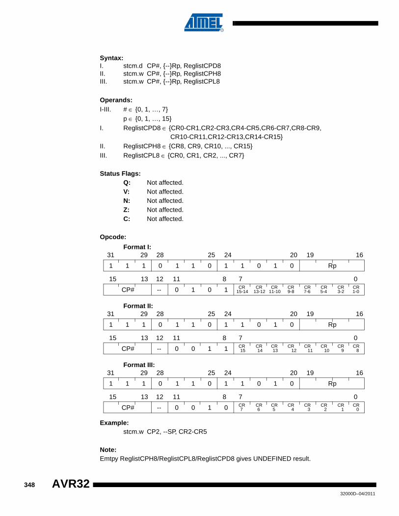
Syntax:I. stcm.d CP#, {--}Rp, ReglistCPD8II. stcm.w CP#, {--}Rp, ReglistCPH8 III. stcm.w CP#, {--}Rp, ReglistCPL8
Operands:I-III. # ∈ {0, 1, …, 7}
p ∈ {0, 1, …, 15}I. ReglistCPD8 ∈ {CR0-CR1,CR2-CR3,CR4-CR5,CR6-CR7,CR8-CR9,
CR10-CR11,CR12-CR13,CR14-CR15}II. ReglistCPH8 ∈ {CR8, CR9, CR10, ..., CR15}III. ReglistCPL8 ∈ {CR0, CR1, CR2, ..., CR7}
Status Flags:Q: Not affected.V: Not affected.N: Not affected.Z: Not affected.C: Not affected.
Opcode:
Format I:
Format II:
Format III:
Example:stcm.w CP2, --SP, CR2-CR5
Note:Emtpy ReglistCPH8/ReglistCPL8/ReglistCPD8 gives UNDEFINED result.
1 1 1 0 1 0 1 1 0 1 0 Rp
31 29 28 25 24 20 19 16
CP# -- 0 1 0 1 CR
15 13 12 11 8 7 0
1
15-14CR
13-12CR
11-10CR9-8
CR7-6
CR5-4
CR3-2
CR1-0
1 1 1 0 1 0 1 1 0 1 0 Rp
31 29 28 25 24 20 19 16
CP# -- 0 0 1 1 CR
15 13 12 11 8 7 0
1
15CR
14CR
13CR 12
CR 11
CR 10
CR 9
CR 8
1 1 1 0 1 0 1 1 0 1 0 Rp
31 29 28 25 24 20 19 16
CP# -- 0 0 1 0 CR
15 13 12 11 8 7 0
1
7CR
6CR
5CR 4
CR 3
CR 2
CR 1
CR 0
34832000D–04/2011
AVR32
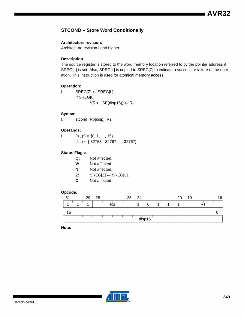
AVR32
STCOND – Store Word Conditionally
Architecture revision:Architecture revision1 and higher.
DescriptionThe source register is stored to the word memory location referred to by the pointer address if SREG[L] is set. Also, SREG[L] is copied to SREG[Z] to indicate a success or failure of the oper-ation. This instruction is used for atomical memory access.
Operation:I. SREG[Z] ← SREG[L];
If SREG[L] *(Rp + SE(disp16)) ← Rs;
Syntax:I. stcond Rp[disp], Rs
Operands:I. {s , p} ∈ {0, 1, …, 15}
disp ∈ {-32768, -32767, ..., 32767}
Status Flags:Q: Not affected.V: Not affected.N: Not affected.Z: SREG[Z] ← SREG[L].C: Not affected.
Opcode:
Note:
1 1 1 Rp 1 0 1 1 1 Rs
31 29 28 25 24 20 19 16
disp16
15 0
34932000D–04/2011

STDSP – Store Stack-Pointer Relative
Architecture revision:Architecture revision1 and higher.
DescriptionStores the source register value to the memory location referred to specified by the Stack Pointer and the displacement.
Operation:I. *( (SP && 0xFFFF_FFFC) + (ZE(disp7) << 2) ) ← Rs;
Syntax:I. stdsp SP[disp], Rs
Operands:I. disp ∈ {0, 4, ..., 508}
s ∈ {0, 1, …, 15}
Status Flags:Q: Not affectedV: Not affectedN: Not affectedZ: Not affectedC: Not affected
Opcode:
0 1 0 1 0 disp7 Rs
15 13 12 11 10 4 3 0
35032000D–04/2011
AVR32
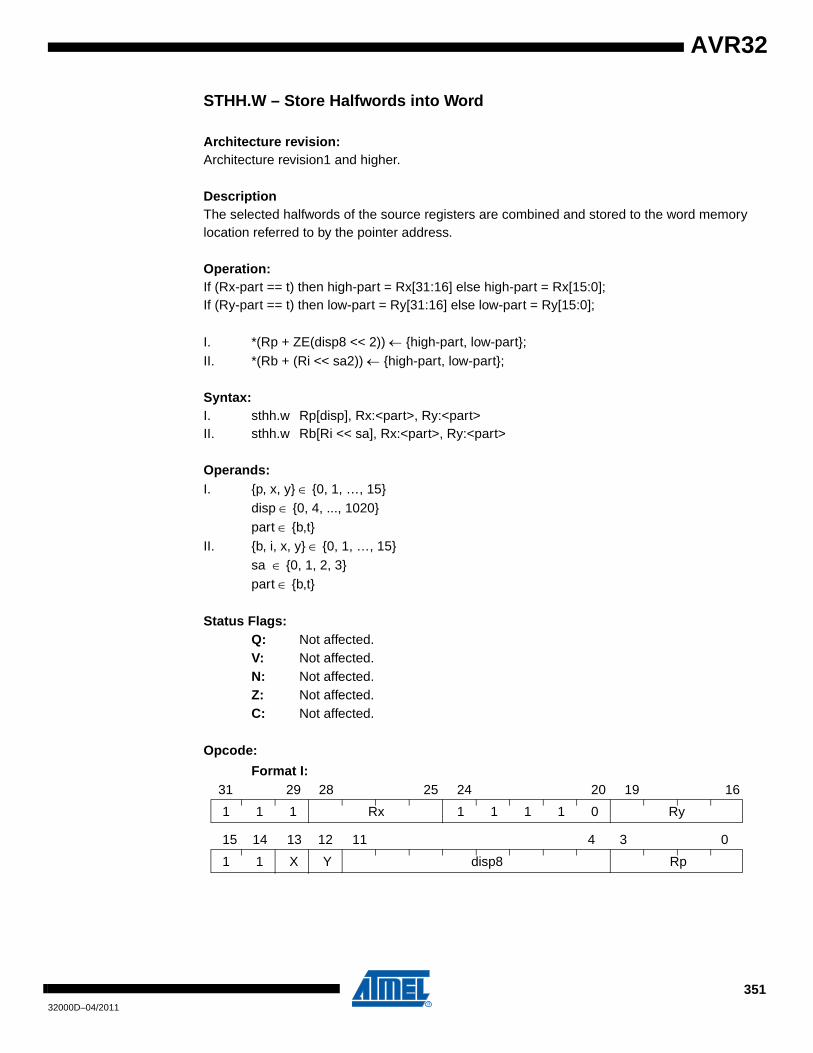
AVR32
STHH.W – Store Halfwords into Word
Architecture revision:Architecture revision1 and higher.
DescriptionThe selected halfwords of the source registers are combined and stored to the word memory location referred to by the pointer address.
Operation:If (Rx-part == t) then high-part = Rx[31:16] else high-part = Rx[15:0];If (Ry-part == t) then low-part = Ry[31:16] else low-part = Ry[15:0];
I. *(Rp + ZE(disp8 << 2)) ← {high-part, low-part};II. *(Rb + (Ri << sa2)) ← {high-part, low-part};
Syntax:I. sthh.w Rp[disp], Rx:<part>, Ry:<part>II. sthh.w Rb[Ri << sa], Rx:<part>, Ry:<part>
Operands:I. {p, x, y} ∈ {0, 1, …, 15}
disp ∈ {0, 4, ..., 1020}part ∈ {b,t}
II. {b, i, x, y} ∈ {0, 1, …, 15}sa ∈ {0, 1, 2, 3}part ∈ {b,t}
Status Flags:Q: Not affected.V: Not affected.N: Not affected.Z: Not affected.C: Not affected.
Opcode:
Format I:
1 1 1 Rx 1 1 1 1 0 Ry
31 29 28 25 24 20 19 16
1 1 X Y disp8 Rp
15 14 13 12 11 4 3 0
35132000D–04/2011

Format II:
1 1 1 Rx 1 1 1 1 0 Ry
31 29 28 25 24 20 19 16
1 0 X Y Ri 0 0 sa2 Rb
15 14 13 12 11 8 7 6 5 4 3 0
35232000D–04/2011
AVR32
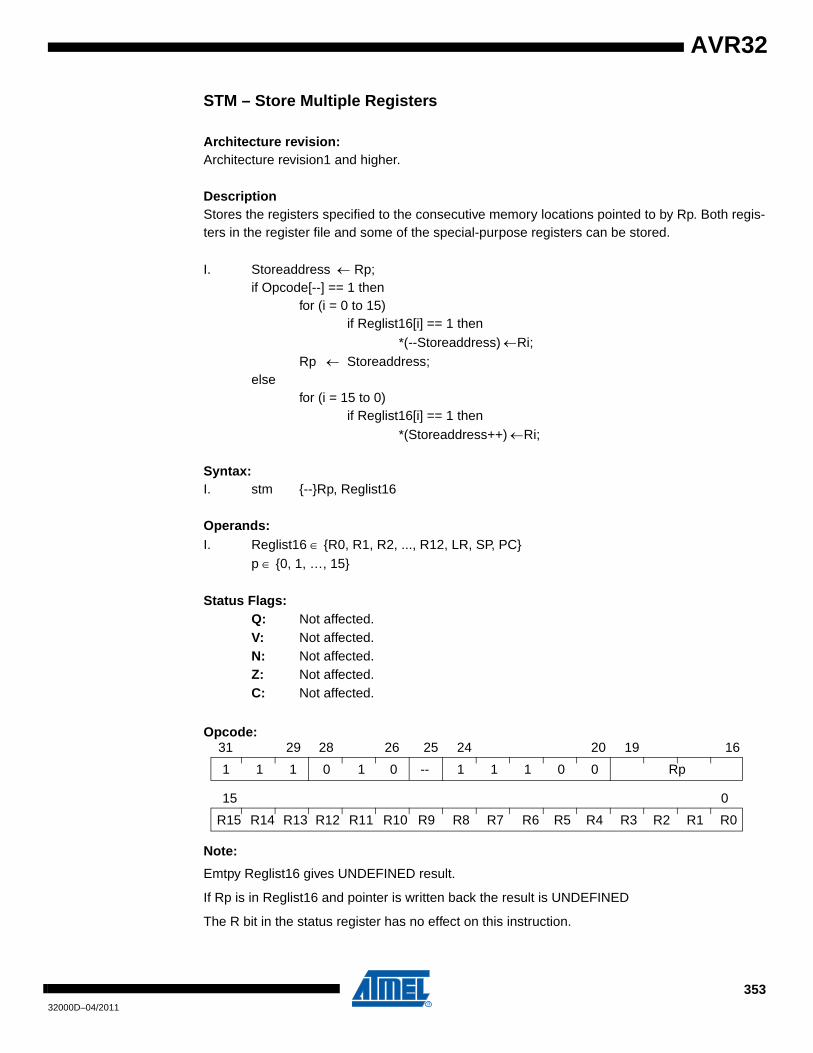
AVR32
STM – Store Multiple Registers
Architecture revision:Architecture revision1 and higher.
DescriptionStores the registers specified to the consecutive memory locations pointed to by Rp. Both regis-ters in the register file and some of the special-purpose registers can be stored.
I. Storeaddress ← Rp;if Opcode[--] == 1 then
for (i = 0 to 15)if Reglist16[i] == 1 then
*(--Storeaddress) ←Ri;Rp ← Storeaddress;
elsefor (i = 15 to 0)
if Reglist16[i] == 1 then *(Storeaddress++) ←Ri;
Syntax:I. stm {--}Rp, Reglist16
Operands:I. Reglist16 ∈ {R0, R1, R2, ..., R12, LR, SP, PC}
p ∈ {0, 1, …, 15}
Status Flags:Q: Not affected.V: Not affected.N: Not affected.Z: Not affected.C: Not affected.
Opcode:
Note:
Emtpy Reglist16 gives UNDEFINED result.
If Rp is in Reglist16 and pointer is written back the result is UNDEFINED
The R bit in the status register has no effect on this instruction.
1 1 1 0 0 -- 1 1 1 0 0 Rp
31 29 28 26 25 24 20 19 16
R15 R14 R13 R12 R11 R10 R9 R8 R7 R6 R5 R4 R3 R2 R1 R0
15 0
1
35332000D–04/2011

STMTS – Store Multiple Registers for Task Switch
Architecture revision:Architecture revision1 and higher.
DescriptionStores the registers specified to the consecutive memory locations pointed to by Rp. The regis-ters specified all reside in the application context.
I. Storeaddress ← Rp;if Opcode[--] == 1 then
for (i = 0 to 15)if Reglist16[i] == 1 then
*(--Storeaddress) ←RiApp;
Rp ← Storeaddress;else
for (i = 15 to 0)if Reglist16[i] == 1 then
*(Storeaddress++) ←RiApp;
Syntax:I. stmts {--}Rp, Reglist16
Operands:I. Reglist16 ∈ {R0, R1, R2, ..., R12, LR, SP}
p ∈ {0, 1, …, 15}
Status Flags:Q: Not affected.V: Not affected.N: Not affected.Z: Not affected.C: Not affected.
Opcode:
Note:Emtpy Reglist16 gives UNDEFINED result.PC in Reglist16 gives UNDEFINED result.
1 1 1 0 1 -- 1 1 1 0 0 Rp
31 29 28 26 25 24 20 19 16
R15 R14 R13 R12 R11 R10 R9 R8 R7 R6 R5 R4 R3 R2 R1 R0
15 0
1
35432000D–04/2011
AVR32
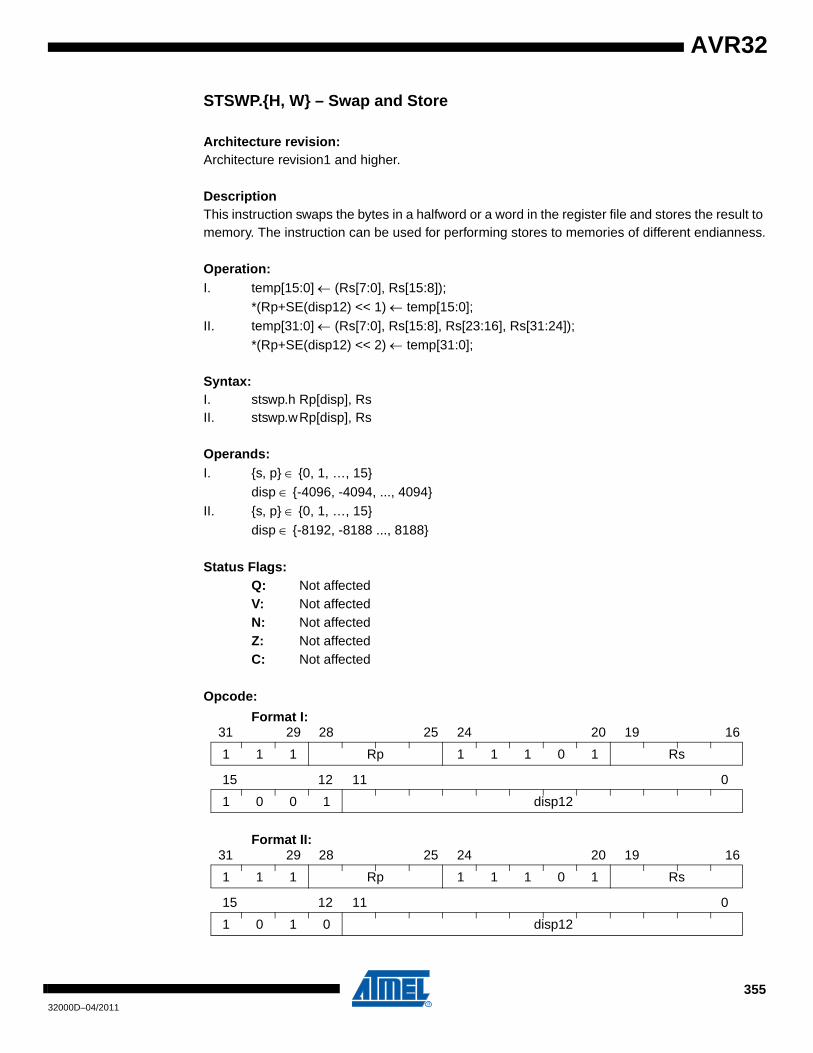
AVR32
STSWP.{H, W} – Swap and Store
Architecture revision:Architecture revision1 and higher.
DescriptionThis instruction swaps the bytes in a halfword or a word in the register file and stores the result to memory. The instruction can be used for performing stores to memories of different endianness.
Operation:I. temp[15:0] ← (Rs[7:0], Rs[15:8]);
*(Rp+SE(disp12) << 1) ← temp[15:0];II. temp[31:0] ← (Rs[7:0], Rs[15:8], Rs[23:16], Rs[31:24]);
*(Rp+SE(disp12) << 2) ← temp[31:0];
Syntax:I. stswp.h Rp[disp], RsII. stswp.wRp[disp], Rs
Operands:I. {s, p} ∈ {0, 1, …, 15}
disp ∈ {-4096, -4094, ..., 4094}II. {s, p} ∈ {0, 1, …, 15}
disp ∈ {-8192, -8188 ..., 8188}
Status Flags:Q: Not affectedV: Not affectedN: Not affectedZ: Not affectedC: Not affected
Opcode:
Format I:
Format II:
1 1 1 Rp 1 1 1 0 1 Rs
31 29 28 25 24 20 19 16
1 0 0 1 disp12
15 12 11 0
1 1 1 Rp 1 1 1 0 1 Rs
31 29 28 25 24 20 19 16
1 0 1 0 disp12
15 12 11 0
35532000D–04/2011
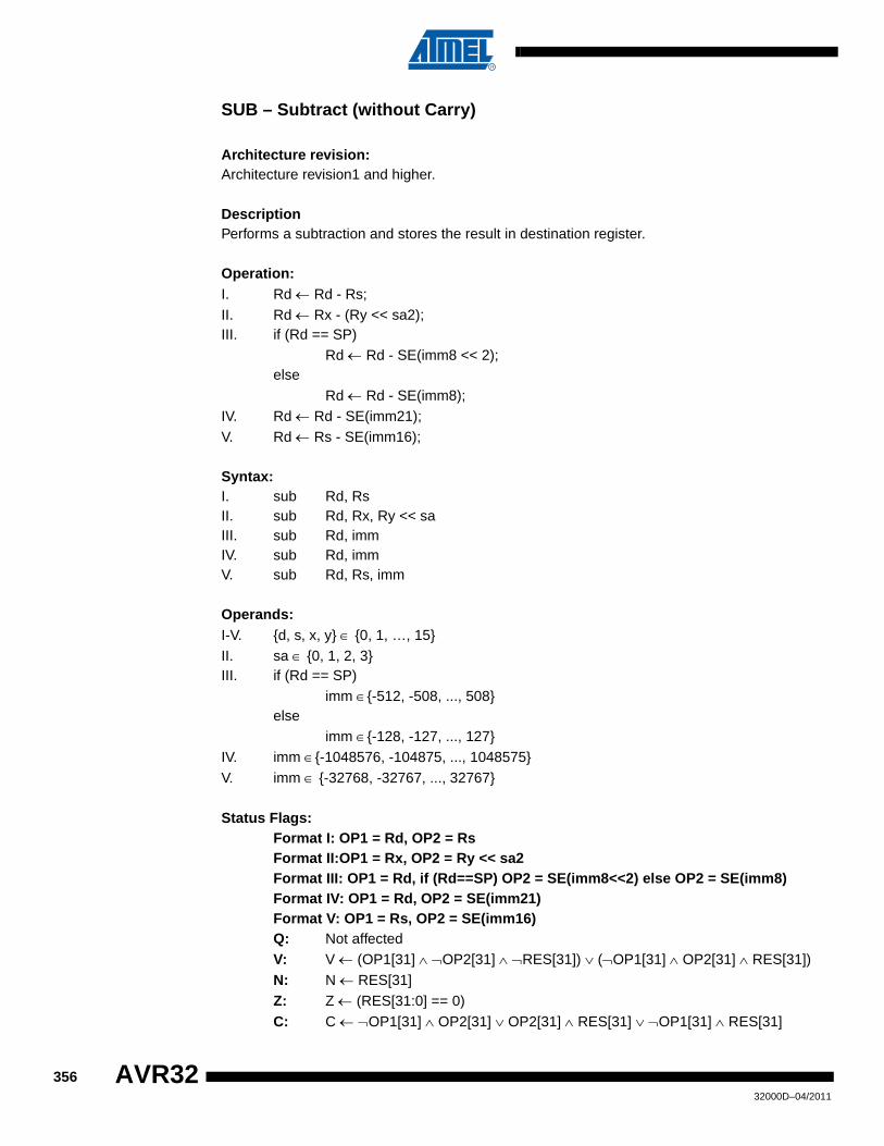
SUB – Subtract (without Carry)
Architecture revision:Architecture revision1 and higher.
DescriptionPerforms a subtraction and stores the result in destination register.
Operation:I. Rd ← Rd - Rs;II. Rd ← Rx - (Ry << sa2);III. if (Rd == SP)
Rd ← Rd - SE(imm8 << 2);else
Rd ← Rd - SE(imm8);IV. Rd ← Rd - SE(imm21);V. Rd ← Rs - SE(imm16);
Syntax:I. sub Rd, RsII. sub Rd, Rx, Ry << saIII. sub Rd, immIV. sub Rd, immV. sub Rd, Rs, imm
Operands:I-V. {d, s, x, y} ∈ {0, 1, …, 15}II. sa ∈ {0, 1, 2, 3}III. if (Rd == SP)
imm ∈{-512, -508, ..., 508}else
imm ∈{-128, -127, ..., 127}IV. imm ∈{-1048576, -104875, ..., 1048575}V. imm ∈ {-32768, -32767, ..., 32767}
Status Flags:Format I: OP1 = Rd, OP2 = RsFormat II:OP1 = Rx, OP2 = Ry << sa2Format III: OP1 = Rd, if (Rd==SP) OP2 = SE(imm8<<2) else OP2 = SE(imm8)Format IV: OP1 = Rd, OP2 = SE(imm21)Format V: OP1 = Rs, OP2 = SE(imm16)Q: Not affectedV: V ← (OP1[31] ∧ ¬OP2[31] ∧ ¬RES[31]) ∨ (¬OP1[31] ∧ OP2[31] ∧ RES[31])N: N ← RES[31]Z: Z ← (RES[31:0] == 0)C: C ← ¬OP1[31] ∧ OP2[31] ∨ OP2[31] ∧ RES[31] ∨ ¬OP1[31] ∧ RES[31]
35632000D–04/2011
AVR32
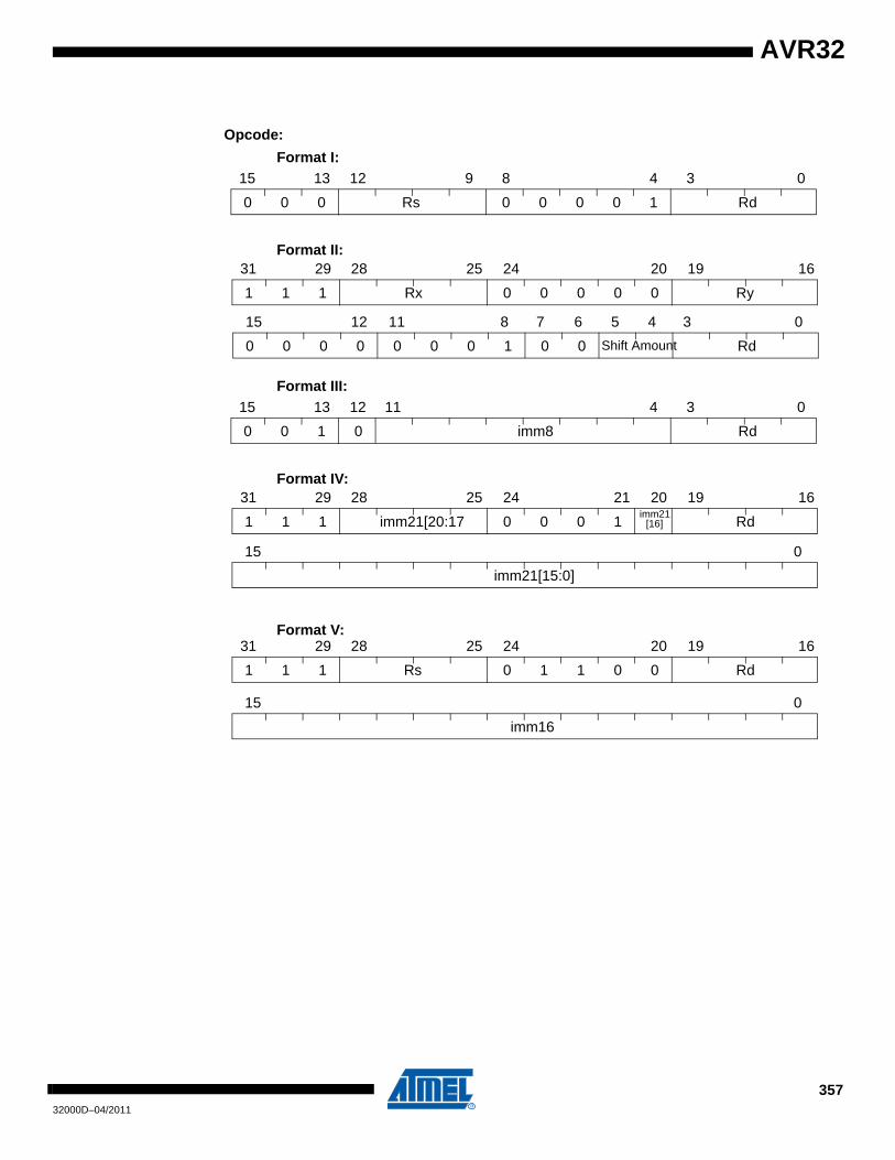
AVR32
Opcode:
Format I:
Format II:
Format III:
Format IV:
Format V:
0 0 0 Rs 0 0 0 0 1 Rd
15 13 12 9 8 4 3 0
1 1 1 Rx 0 0 0 0 0 Ry
31 29 28 25 24 20 19 16
0 0 0 0 0 0 0 1 0 0 Shift Amount Rd
15 12 11 8 7 6 5 4 3 0
0 0 1 0 imm8 Rd
15 13 12 11 4 3 0
1 1 1 imm21[20:17 0 0 0 1imm21
Rd
31 29 28 25 24 21 20 19 16
imm21[15:0]
15 0
[16]
1 1 1 Rs 0 1 1 0 0 Rd
31 29 28 25 24 20 19 16
imm16
15 0
35732000D–04/2011
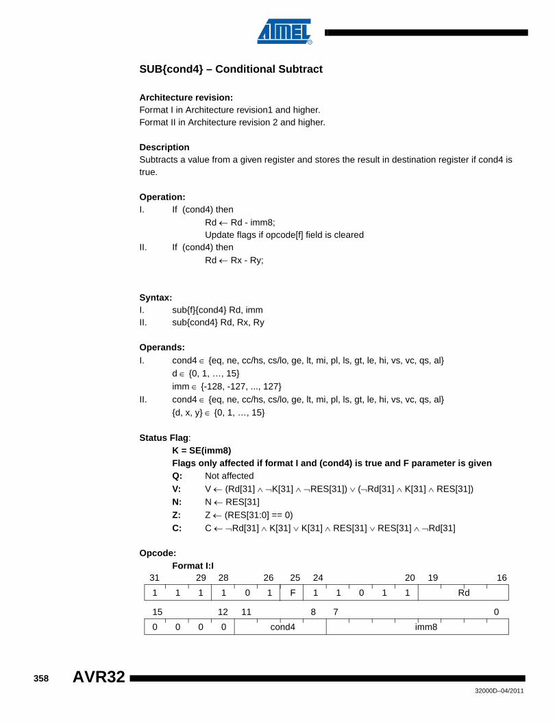
SUB{cond4} – Conditional Subtract
Architecture revision:Format I in Architecture revision1 and higher.Format II in Architecture revision 2 and higher.
DescriptionSubtracts a value from a given register and stores the result in destination register if cond4 is true.
Operation:I. If (cond4) then
Rd ← Rd - imm8;Update flags if opcode[f] field is cleared
II. If (cond4) thenRd ← Rx - Ry;
Syntax:I. sub{f}{cond4} Rd, immII. sub{cond4} Rd, Rx, Ry
Operands:I. cond4 ∈ {eq, ne, cc/hs, cs/lo, ge, lt, mi, pl, ls, gt, le, hi, vs, vc, qs, al}
d ∈ {0, 1, …, 15}imm ∈ {-128, -127, ..., 127}
II. cond4 ∈ {eq, ne, cc/hs, cs/lo, ge, lt, mi, pl, ls, gt, le, hi, vs, vc, qs, al}{d, x, y} ∈ {0, 1, …, 15}
Status Flag:K = SE(imm8)Flags only affected if format I and (cond4) is true and F parameter is givenQ: Not affectedV: V ← (Rd[31] ∧ ¬K[31] ∧ ¬RES[31]) ∨ (¬Rd[31] ∧ K[31] ∧ RES[31])N: N ← RES[31]Z: Z ← (RES[31:0] == 0)C: C ← ¬Rd[31] ∧ K[31] ∨ K[31] ∧ RES[31] ∨ RES[31] ∧ ¬Rd[31]
Opcode:Format I:I
1 1 1 1 1 F 1 1 0 1 1 Rd
31 29 28 26 25 24 20 19 16
0 0 0 0 cond4 imm8
15 12 11 8 7 0
0
35832000D–04/2011
AVR32
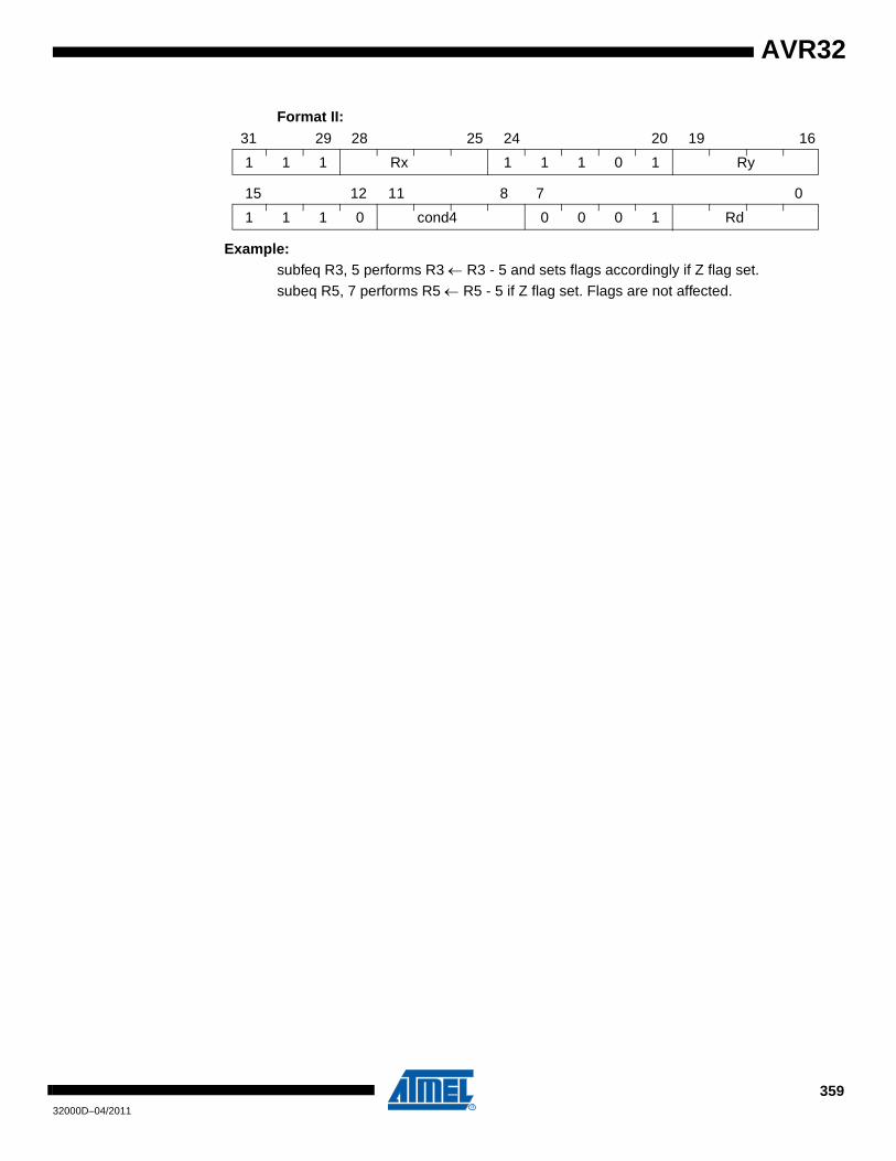
AVR32
Format II:
Example:subfeq R3, 5 performs R3 ← R3 - 5 and sets flags accordingly if Z flag set.subeq R5, 7 performs R5 ← R5 - 5 if Z flag set. Flags are not affected.
1 1 1 1 1 1 0 1 Ry
31 29 28 25 24 20 19 16
1 1 1 0 cond4 0 0 0 1 Rd
15 12 11 8 7 0
Rx
35932000D–04/2011

SUBHH.W– Subtract Halfwords into Word
Architecture revision:Architecture revision1 and higher.
DescriptionSubtracts the two halfword registers specified and stores the result in the destination word-regis-ter. The halfword registers are selected as either the high or low part of the operand registers.
Operation:I. If (Rx-part == t) then operand1 = SE(Rx[31:16]) else operand1 = SE(Rx[15:0]);
If (Ry-part == t) then operand2 = SE(Ry[31:16]) else operand2 = SE(Ry[15:0]);Rd ← operand1 - operand2;
Syntax:I. subhh.wRd, Rx:<part>, Ry:<part>
Operands:I. {d, x, y} ∈ {0, 1, …, 15}
part ∈ {t,b}
Status Flags:OP1 = operand1, OP2 = operand2Q: Not affectedV: V ← (OP1[31] ∧ ¬OP2[31] ∧ ¬RES[31]) ∨ (¬OP1[31] ∧ OP2[31] ∧ RES[31])N: N ← RES[31]Z: Z ← (RES[31:0] == 0)C: C ← ¬OP1[31] ∧ OP2[31] ∨ OP2[31] ∧ RES[31] ∨ ¬OP1[31] ∧ RES[31]
Opcode:
Example:subhh.wR10, R2:t, R3:bwill perform R10 ← SE(R2[31:16]) - SE(R3[15:0])
1 1 1 Rx 0 0 0 0 0 Ry
31 29 28 25 24 20 19 16
0 0 0 0 1 1 1 1 0 0 X Y Rd
15 12 11 6 5 4 3 0
36032000D–04/2011
AVR32

AVR32
SWAP.B – Swap Bytes
Architecture revision:Architecture revision1 and higher.
DescriptionSwaps different parts of a register.
Operation:I. Temp ← Rd;
Rd[31:24] ← Temp[7:0];Rd[23:16] ← Temp[15:8];Rd[15:8] ← Temp[23:16];Rd[7:0] ← Temp[31:24];
Syntax:I. swap.b Rd
Operands:I. d ∈ {0, 1, …, 15}
Status Flags:Q: Not affected.V: Not affected.N: Not affected.Z: Not affected.C: Not affected.
Opcode:
0 1 0 1 1 1 0 0 1 0 1 1 Rd
15 13 12 9 8 4 3 0
36132000D–04/2011
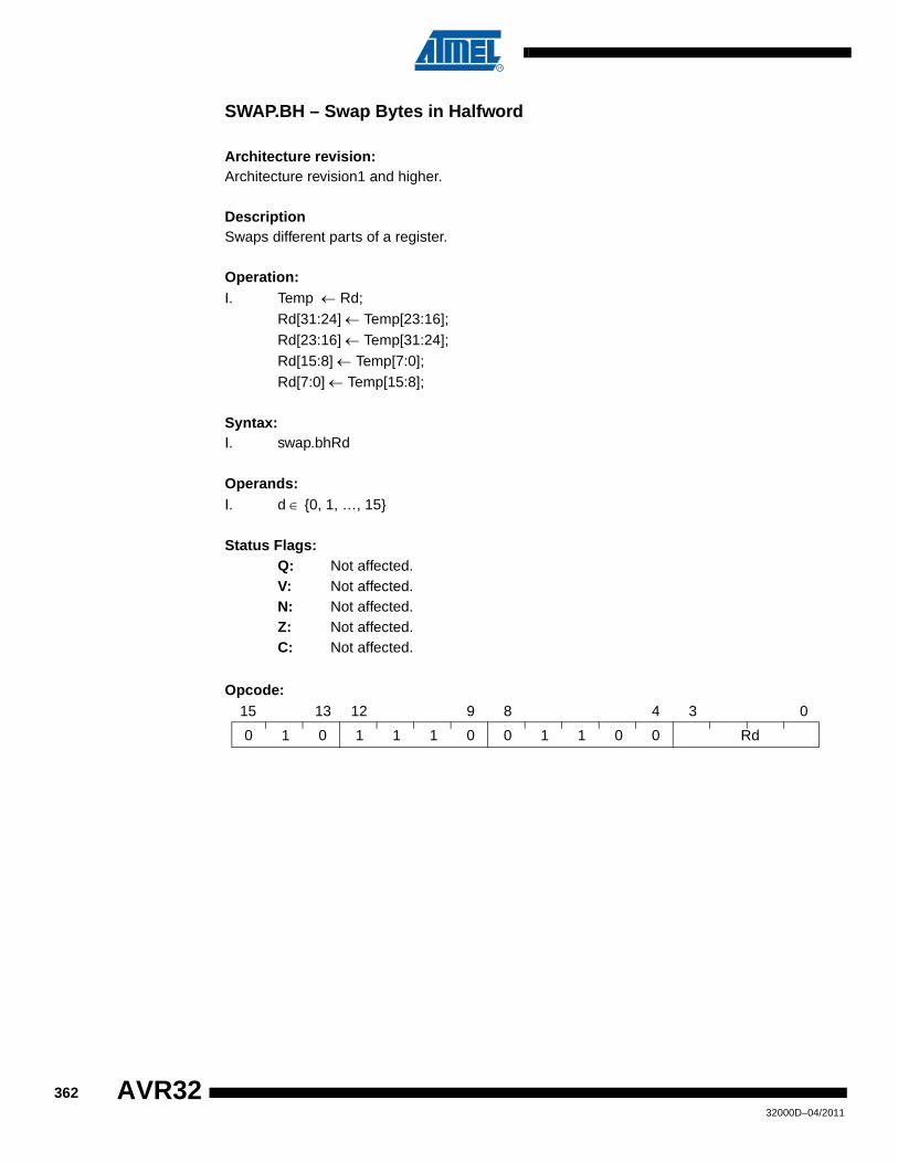
SWAP.BH – Swap Bytes in Halfword
Architecture revision:Architecture revision1 and higher.
DescriptionSwaps different parts of a register.
Operation:I. Temp ← Rd;
Rd[31:24] ← Temp[23:16];Rd[23:16] ← Temp[31:24];Rd[15:8] ← Temp[7:0];Rd[7:0] ← Temp[15:8];
Syntax:I. swap.bhRd
Operands:I. d ∈ {0, 1, …, 15}
Status Flags:Q: Not affected.V: Not affected.N: Not affected.Z: Not affected.C: Not affected.
Opcode:
0 1 0 1 1 1 0 0 1 1 0 0 Rd
15 13 12 9 8 4 3 0
36232000D–04/2011
AVR32
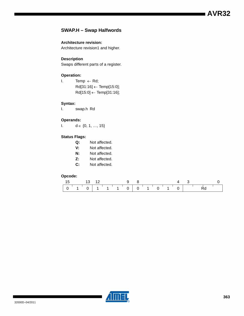
AVR32
SWAP.H – Swap Halfwords
Architecture revision:Architecture revision1 and higher.
DescriptionSwaps different parts of a register.
Operation:I. Temp ← Rd;
Rd[31:16] ← Temp[15:0];Rd[15:0] ← Temp[31:16];
Syntax:I. swap.h Rd
Operands:I. d ∈ {0, 1, …, 15}
Status Flags:Q: Not affected.V: Not affected.N: Not affected.Z: Not affected.C: Not affected.
Opcode:
0 1 0 1 1 1 0 0 1 0 1 0 Rd
15 13 12 9 8 4 3 0
36332000D–04/2011
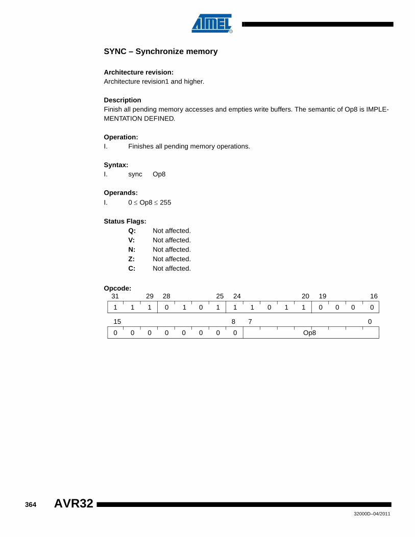
SYNC – Synchronize memory
Architecture revision:Architecture revision1 and higher.
DescriptionFinish all pending memory accesses and empties write buffers. The semantic of Op8 is IMPLE-MENTATION DEFINED.
Operation: I. Finishes all pending memory operations.
Syntax:I. sync Op8
Operands:I. 0 ≤ Op8 ≤ 255
Status Flags:Q: Not affected.V: Not affected.N: Not affected.Z: Not affected.C: Not affected.
Opcode:
1 1 1 0 0 1 1 1 0 1 1 0 0 0
31 29 28 25 24 20 19 16
0 0 0 0 0 0 0 0 Op8
15 8 7 0
1 0
36432000D–04/2011
AVR32

AVR32
TLBR – Read TLB Entry
Architecture revision:Architecture revision1 and higher.
DescriptionRead the contents of the addressed ITLB or DTLB Entry into TLBEHI and TLBELO.
Operation:I. if (TLBEHI[I] == 1)
{TLBEHI, TLBELO} ←ITLB[MMUCR[IRP]];else
{TLBEHI, TLBELO} ←DTLB[MMUCR[DRP]];
Syntax:I. tlbr
Operands:None
Status Flags:Q: Not affected.V: Not affected.N: Not affected.Z: Not affected.C: Not affected.
Opcode:
Note:This instruction can only be executed in a privileged mode.
1 1 0 1 0 1 1 0 0 1 0 0 0 0 1 1
15 9 8 4 3 0
36532000D–04/2011
TLBS – Search TLB For Entry
Architecture revision:Architecture revision1 and higher.
DescriptionSearch the addressed TLB for an entry matching TLB Entry High and Low (TLBEHI/TLBELO) registers. Return a pointer to the entry in MMUCR[IRP] or MMUCR[DRP] if a match found, oth-erwise set the Not Found bit in the MMU control register, MMUCR[N].
Operation:I. MMUCR[N] ←1;
if (TLBEHI[I] == 1)TlbToSearch ←ITLB;
elseTlbToSearch ←DTLB;
endif;
for (i = 0 to TLBToSearchEntries-1)if ( Compare(TlbToSearch[i]VPN, VA, TlbToSearch[i]SZ, TlbToSearch[i]V) )// VPN and VA matches for the given page size and entry valid
if ( SharedVMM or (PrivateVMM and ( TlbToSearch[i]G or (TlbToSearch[i]ASID==TLBEHI[ASID]) ) ) )ptr ← i;MMUCR[N] ←0;
endif;endif;
endfor;if (TLBEHI[I] == 1)
MMUCR[IRP] ←ptr;else
MMUCR[DRP] ←ptr;endif;
Syntax:I. tlbsOperands:
None
Status Flags:Q: Not affected.V: Not affected.N: Not affected.Z: Not affected.C: Not affected.
36632000D–04/2011
AVR32

AVR32
Opcode:
Note:This instruction can only be executed in a privileged mode.
1 1 0 1 0 1 1 0 0 1 0 1 0 0 1 1
15 9 8 4 3 0
36732000D–04/2011
TLBW – Write TLB Entry
Architecture revision:Architecture revision1 and higher.
DescriptionWrite the contents of the TLB Entry High and Low (TLBEHI/TLBELO) registers into the addressed TLB entry.
Operation:I. if (TLBEHI[I] == 1)
ITLB[MMUCR[IRP]] ← {TLBEHI, TLBELO};else
ITLB[MMUCR[DRP]] ← {TLBEHI, TLBELO};
Syntax:I. tlbw
Operands:None
Status Flags:Q: Not affected.V: Not affected.N: Not affected.Z: Not affected.C: Not affected.
Opcode:
Note:This instruction can only be executed in a privileged mode.
1 1 0 1 0 1 1 0 0 1 1 0 0 0 1 1
15 9 8 4 3 0
36832000D–04/2011
AVR32
AVR32
TNBZ – Test if No Byte is Equal to Zero
Architecture revision:Architecture revision1 and higher.
DescriptionIf any of the bytes 0,1,2,3 in the word is zero, the SR[Z] flag is set.
Operation:I. if (Rd[31:24] == 0 ∨
Rd[23:16] == 0 ∨ Rd[15:8] == 0 ∨ Rd[7:0] == 0 )
SR[Z] ← 1;else
SR[Z] ← 0;
Syntax:I. tnbz Rd
Operands:I. d ∈ {0, 1, …, 15}
Status Flags:Q: Not affected.V: Not affected.N: Not affected.Z: Z ← (Rd[31:24] == 0 ∨ Rd[23:16] == 0 ∨ Rd[15:8] == 0 ∨ Rd[7:0] == 0 )
C: Not affected.
Opcode:
0 1 0 1 1 1 0 0 1 1 1 0 Rd
15 13 12 9 8 4 3 0
36932000D–04/2011

TST – Test Register
Architecture revision:Architecture revision1 and higher.
DescriptionTest register. Used to check if a subset of a register includes one or more set bits. No writeback of the result is performed, but the flags are set.
Operation:I. Rd ∧ Rs;
Syntax:I. tst Rd, Rs
Operands:I. {d,s} ∈ {0, 1, …, 15}
Status FlagsQ: Not affectedV: Not affectedN: N ← RES[31]Z: Z ← (RES[31:0] == 0)C: Not affected
Opcode(s)
0 0 0 Rs 0 0 1 1 1 Rd
15 13 12 9 8 4 3 0
37032000D–04/2011
AVR32

AVR32
XCHG – Exchange Register and Memory
Architecture revision:Architecture revision1 and higher.
DescriptionReads a word from memory pointed to by Rx into register Rd, and writes the value of register Ry to memory. This instruction can be used to implement binary semaphores (mutexes). The stcond instruction should be used to implement counting semaphores.
Operation: I. Temp ← *(Rx);
*(Rx) ← Ry;Rd ← Temp;
Syntax:I. xchg Rd, Rx, Ry
Operands:I. {d,x,y} ∈ {0, 1, …, 14}
Status Flags:Q: Not affectedV: Not affectedN: Not affectedZ: Not affectedC: Not affected
Opcode:
Note:If R15 is used as Rd, Rx or Ry, the result is UNDEFINED.If Rd = Ry, the result is UNDEFINED.If Rd = Rx, the result is UNDEFINED.
1 1 1 Rx 0 0 0 0 0 Ry
31 29 28 25 24 20 19 16
0 0 0 0 1 0 1 1 0 1 0 0 Rd
15 12 11 4 3 0
37132000D–04/2011

37232000D–04/2011
AVR32
AVR32
10. Revision History
10.1 Rev. 32000A-02/2006
10.2 Rev. 32000B-11/2007
10.3 Rev. 32000C-08/2009
10.4 Rev. 32000D-04/2011
1. Initial version.
1. Improved description of RETE in Instruction Set Chapter.2. Corrected description of STC.D in Instruction Set Chapter.3. Added micro-TLB miss performance counting.4. Added clear-on-compare functionality to COUNT system register5. Updated MPU description to match implementation6. Added new architecture revision 2 instructions
1. Corrected typos in the MOVH instruction description.2. Corrected Reset address typo in chapter 7.3.1.13. Corrected typos in RETE, DIVS and DIVU detailed instruction set descriptions.4. Described new architecture revision 3 secure execution state.5. Automatic clear of COUNT on COMPARE match can now be overridden, usually
by writing a bit in the implementation’s CPUCR register.
1. FlashVault™ description added2. Instruction syntax: Each Ri<part> has been replaced by Ri:<part> in the instruc-
tion set summary and descriptions3. Added description of bit 7 in Op8 in sleep instruction4. Parantheses added to shift instruction descriptions to clarify the order of the
operations5. Added cond4 to ld.sb, ld.ub, ld.sh, ld.uh, ld.w, st.b, st.h, st.w instruction descrip-
tion syntax6. SE replaced by ZE in st.w{cond4} in the Instruction Set Summary table
37332000D–04/2011

37432000D–04/2011
AVR32
AVR32
Table of contents
Feature Summary...................................................................................... 1
1 Introduction .............................................................................................. 2
1.1 The AVR family ..................................................................................................2
1.2 The AVR32 Microprocessor Architecture .........................................................2
1.3 Microarchitectures .............................................................................................4
2 Programming Model ................................................................................ 5
2.1 Data Formats .....................................................................................................5
2.2 Data Organization ..............................................................................................5
2.3 Instruction Organization .....................................................................................6
2.4 Processor States ...............................................................................................7
2.5 Entry and Exit Mechanism .................................................................................8
2.6 Register File ......................................................................................................8
2.7 The Stack Pointer ............................................................................................10
2.8 The Program Counter ......................................................................................11
2.9 The Link Register ............................................................................................11
2.10 The Status Register .........................................................................................11
2.11 System registers ..............................................................................................14
2.12 Recommended Call Convention ......................................................................26
3 Java Extension Module ......................................................................... 27
3.1 The AVR32 Java Virtual Machine ....................................................................27
4 Secure state ............................................................................................ 31
4.1 Mechanisms implementing the Secure State ..................................................31
4.2 Secure state programming model ...................................................................32
4.3 Details on Secure State implementation .........................................................33
5 Memory Management Unit .................................................................... 35
5.1 Memory map in systems with MMU .................................................................35
5.2 Understanding the MMU ..................................................................................37
5.3 Operation of the MMU and MMU exceptions ..................................................47
6 Memory Protection Unit ........................................................................ 51
6.1 Memory map in systems with MPU .................................................................51
6.2 Understanding the MPU ..................................................................................51
6.3 Example of MPU functionality ..........................................................................55
i32000D–04/2011

7 Performance counters ........................................................................... 57
7.1 Overview ..........................................................................................................57
7.2 Registers .........................................................................................................57
7.3 Monitorable events ..........................................................................................59
7.4 Usage ..............................................................................................................60
8 Event Processing ................................................................................... 63
8.1 Event handling in AVR32A ..............................................................................63
8.2 Event handling in AVR32B ..............................................................................64
8.3 Entry points for events .....................................................................................66
8.4 Event priority ....................................................................................................92
8.5 Event handling in secure state ........................................................................92
9 AVR32 RISC Instruction Set .................................................................. 93
9.1 Instruction Set Nomenclature ..........................................................................93
9.2 Instruction Formats ..........................................................................................97
9.3 Instruction Set Summary ...............................................................................106
9.4 Base Instruction Set Description ...................................................................122
10 Revision History ................................................................................... 373
10.1 Rev. 32000A-02/2006 ....................................................................................373
10.2 Rev. 32000B-11/2007 ....................................................................................373
10.3 Rev. 32000C-08/2009 ...................................................................................373
10.4 Rev. 32000D-04/2011 ...................................................................................373
Table of contents ....................................................................................... i
ii32000D–04/2011
AVR32
Atmel Corporation2325 Orchard ParkwaySan Jose, CA 95131USATel: (+1)(408) 441-0311Fax: (+1)(408) 487-2600 www.atmel.com
Atmel Asia LimitedUnit 1-5 & 16, 19/FBEA Tower, Millennium City 5418 Kwun Tong RoadKwun Tong, KowloonHONG KONGTel: (+852) 2245-6100Fax: (+852) 2722-1369
Atmel Munich GmbHBusiness CampusParkring 4D-85748 Garching b. MunichGERMANYTel: (+49) 89-31970-0Fax: (+49) 89-3194621
Atmel Japan9F, Tonetsu Shinkawa Bldg.1-24-8 ShinkawaChuo-ku, Tokyo 104-0033JAPANTel: (+81)(3) 3523-3551Fax: (+81)(3) 3523-7581
© 2011 Atmel Corporation. All rights reserved. / Rev. CORP072610
Atmel®, logo and combinations thereof, and others are registered trademarks or trademarks of Atmel Corporation or its subsidiaries. Other terms and product names may be trademarks of others.
Disclaimer: The information in this document is provided in connection with Atmel products. No license, express or implied, by estoppel or otherwise, to any intellectual property right is granted by this document or in connection with the sale of Atmel products. EXCEPT AS SET FORTH IN THE ATMEL TERMS AND CONDITIONS OF SALES LOCATED ON THE ATMEL WEBSITE, ATMEL ASSUMES NO LIABILITY WHATSOEVER AND DISCLAIMS ANY EXPRESS, IMPLIED OR STATUTORY WARRANTY RELATING TO ITS PRODUCTS INCLUDING, BUT NOT LIMITED TO, THE IMPLIED WARRANTY OF MERCHANTABILITY, FITNESS FOR A PARTICULAR PURPOSE, OR NON-INFRINGEMENT. IN NO EVENT SHALL ATMEL BE LIABLE FOR ANY DIRECT, INDIRECT, CONSEQUENTIAL, PUNITIVE, SPECIAL OR INCIDENTAL DAMAGES (INCLUDING, WITHOUT LIMITATION, DAMAGES FOR LOSS AND PROF-ITS, BUSINESS INTERRUPTION, OR LOSS OF INFORMATION) ARISING OUT OF THE USE OR INABILITY TO USE THIS DOCUMENT, EVEN IF ATMEL HAS BEEN ADVISED OF THE POSSIBILITY OF SUCH DAMAGES. Atmel makes no representations or warranties with respect to the accuracy or com-pleteness of the contents of this document and reserves the right to make changes to specifications and product descriptions at any time without notice. Atmel does not make any commitment to update the information contained herein. Unless specifically provided otherwise, Atmel products are not suit-able for, and shall not be used in, automotive applications. Atmel products are not intended, authorized, or warranted for use as components in applica-tions intended to support or sustain life.
32000D–04/2011