Embed Size (px)
Citation preview
Rochester Institute of Technology Rochester Institute of Technology
RIT Scholar Works RIT Scholar Works
Theses
12-2020
Backplane System Design Considerations for Micro LED Displays Backplane System Design Considerations for Micro LED Displays
Kush Benara [email protected]
Follow this and additional works at: https://scholarworks.rit.edu/theses
Recommended Citation Recommended Citation Benara, Kush, "Backplane System Design Considerations for Micro LED Displays" (2020). Thesis. Rochester Institute of Technology. Accessed from
This Thesis is brought to you for free and open access by RIT Scholar Works. It has been accepted for inclusion in Theses by an authorized administrator of RIT Scholar Works. For more information, please contact [email protected].
BACKPLANE SYSTEM DESIGN CONSIDERATIONS FOR
MICRO LED DISPLAYS
KUSH BENARA
DECEMBER 2020
BACKPLANE SYSTEM DESIGN CONSIDERATIONS FOR MICRO LED DISPLAYS
KUSH BENARA DECEMBER 2020
A THESIS SUBMITTED IN PARTIAL FULFILLMENT OF THE REQUIREMENTS FOR THE DEGREE OF
MASTER OF SCIENCE
IN
MICROELECTRONIC ENGINEERING
DEPARTMENT OF ELECTRICAL AND MICROELECTRONIC ENGINEERING
ii | P a g e
BACKPLANE SYSTEM DESIGN CONSIDERATIONS FOR MICRO LED DISPLAYS
KUSH BENARA
COMMITTEE APPROVAL
Dr. Karl Hirschman, Advisor Date Professor, Electrical & Microelectronic Engineering Dr. Robert Pearson, Committee Member Date Associate Professor, Electrical & Microelectronic Engineering
Mark Indovina, Committee Member Date Senior Lecturer, Electrical & Microelectronic Engineering
Dr. Sean Rommel Date Microelectronic Engineering Program Director
DEPARTMENT OF ELECTRICAL AND MICROELECTRONIC ENGINEERING

iii | P a g e
ACKNOWLEDGMENTS
I would first like to thank my advisor, Dr. Karl Hirschman, for his tremendous guidance and
support through this project. I would also like to thank my committee members, Dr. Robert Pearson
and Mark Indovina, for their time and efforts in shaping and revising this work.
I would like to thank Corning.Inc for supporting and providing the funding for this work.
Thank you to RIT for giving me an opportunity to study and move ahead in life.
I would also like to thank my team mates from the uLED project who have helped me
throughout this project. This includes Vaishali V, Mohammed Mueen, Conrad Mizack, and Hector
Rubio.
Finally, I would also like to thank all my family and friends who have supported me throughout
my graduate career and my life. Thank you to the Benara family for making me who I am today,
without the hard work and sacrifices made by my ancestors I wouldn’t have made it this far.
Above all else, I would like to thank my Mother for giving me an education and always making
me take the right decisions in life.
iv | P a g e
Contents
Signature Sheet ii
Table of Contents iv
List of Figures vii
List of Tables xi
Abstract xiii
I Introduction
1.1 Working Principle of FPD’s . . . . . . 1
1.2 Pixel Addressing Scheme . . . . . . 6
1.3 IGZO Material for TFTs . . . . . . 8
1.4 Flat Panel Display systems . . . . . . 9
1.5 Thesis goals and objectives . . . . . . 10
1.6 Chapter Organization . . . . . . 11
II Design Considerations for a uLED display backplane
2.1 Pixel Circuit . . . . . . 13
2.2 TFT and uLED model . . . . . . 16
2.2.1 TFT model . . . . . . 16
2.2.2 uLED model . . . . . . 18
2.3 System Control . . . . . . 20
2.3.1 Gate and Source Drivers . . . . . 22
2.3.2 Timing Controller . . . . . . 23
v | P a g e
2.3.3 PWM for brightness control . . . . . 23
2.4 Parasitic resistance and capacitance . . . . . 24
2.5 Summary . . . . . 25
III Design of the FPGA code for the model board
3.1 Model Board . . . . . 26
3.2 FPGA Code Development . . . . . 29
3.2.1 Controller . . . . . 29
3.2.2 Shift Register Row and Column controller . . 32
3.3 Row and Column timing . . . . . 36
3.4 Summary . . . . . 38
IV Impact of Line resistances and RGB pixel design
4.1 Pixel circuit Simulations and impact of parasitics elements . 39
4.2 Pixel Circuit simulations for Row-Line and Column-Line
delay estimations . . . . . . . 50
4.3 Pixel Circuit Simulations to estimate the IR loss Effects . . 55
4.4 RGB pixel design . . . . . . . . . . . . . . . . 61
4.5 Summary . . . . . . . . . . . . . . . . 65
V Electrical bonding between the glass and PCB
5.1 Bonding Techniques . . . . . . . 66
5.1.1 Flip Chip Bonding . . . . . . 65
5.1.2 ACF Bonding . . . . . . 67
5.2 PCB and glass bonding . . . . . . 69
5.3 Wrap-around electrodes . . . . . . 71
vi | P a g e
5.4 Summary . . . . . . . . 74
VI Conclusion and Future Works
6.1 Conclusion . . . . . . . . 76
6.2 Future works . . . . . . . . 77
References . . . . . . . . . . . . . . . . . . 78
Appendix A . . . . . . . . . . . . . . . . . 81
Appendix B . . . . . . . . . . . . . . . . . 82
Appendix C . . . . . . . . . . . . . . . . . 88
vii | P a g e
List of Figures
1.1 Structure of a LCD display . . . . . . . 2
1.2 (a) LC arrangement in a LCD in the absence of an electric field.
(b)LC arrangement in a LCD when an electric field is applied across
the electrodes . . . . . . . . . 3
1.3 OLED stack . . . . . . . . . 5
1.4 uLED stack . . . . . . . . . 5
1.5 A passive matrix driving scheme to drive an emissive device . . 6
1.6 An active matrix driving scheme to drive an emissive device . . 7
1.7 Cross section schematic of a bottom gate a-IGZO TFT . . 8
1.8 A FPD system consisting of an electronics circuit board and display
panel with the TFTs . . . . . . . . 10
2.1 A 2T1C circuit for driving a uLED . . . . . . 14
2.2 BG IGZO transistors unaffected by a PBS at a VG = +10 V with S/D at
reference ground . . . . . . . . 15
2.3 BG IGZO transistors exhibiting a shift in the threshold voltage due to
NBS a VG = -10 V with S/D at reference ground . . . . 15
2.4 Measured vs simulated output characteristics for a L=4 µm & W=24 µm
channel IGZO TFT . . . . . . . . 17
viii | P a g e
2.5 Measured vs simulated transfer characteristics for a L= 4 µm & W=24 µm
channel IGZO TFT . . . . . . . . 18
2.6 uLED devices of dimensions 20um by 50 um fabricated on a source wafer . 18
2.7 I-V characteristics of the uLED simulated in virtuoso using the
model equations . . . . . . . . 20
2.8 Architecture for an a-Si AMLCD driver . . . . . 20
2.9 A gate driver architecture for TFT matrix . . . . . 22
2.10 A PWM scheme showing a 25%, 50%, 75% duty cycle for controlling
the brightness . . . . . . . . 24
3.0 a) A 10x10 model board for FPGA code development
b) A schematic of the model board . . . . 27
3.1 Working of a Serial-in parallel-out shift register . . . 28
3.2 Timing diagram of an 8-bit shift register (CD74HC595N) . . . 28
3.3 Architecture for the FPGA code for the 10x10 model board. . . 31
3.4 State machine inside the controller for fetching data from the BRAM . . 32
3.5 An AXI4 lite read transaction between a memory and a master device . . 32
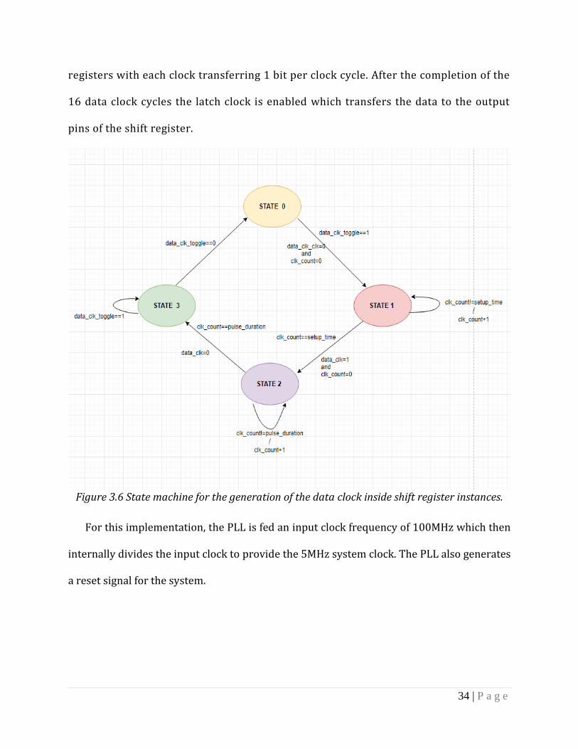
3.6 State machine for the generation of the data clock inside shift register
instances . . . . . . . . . . 34
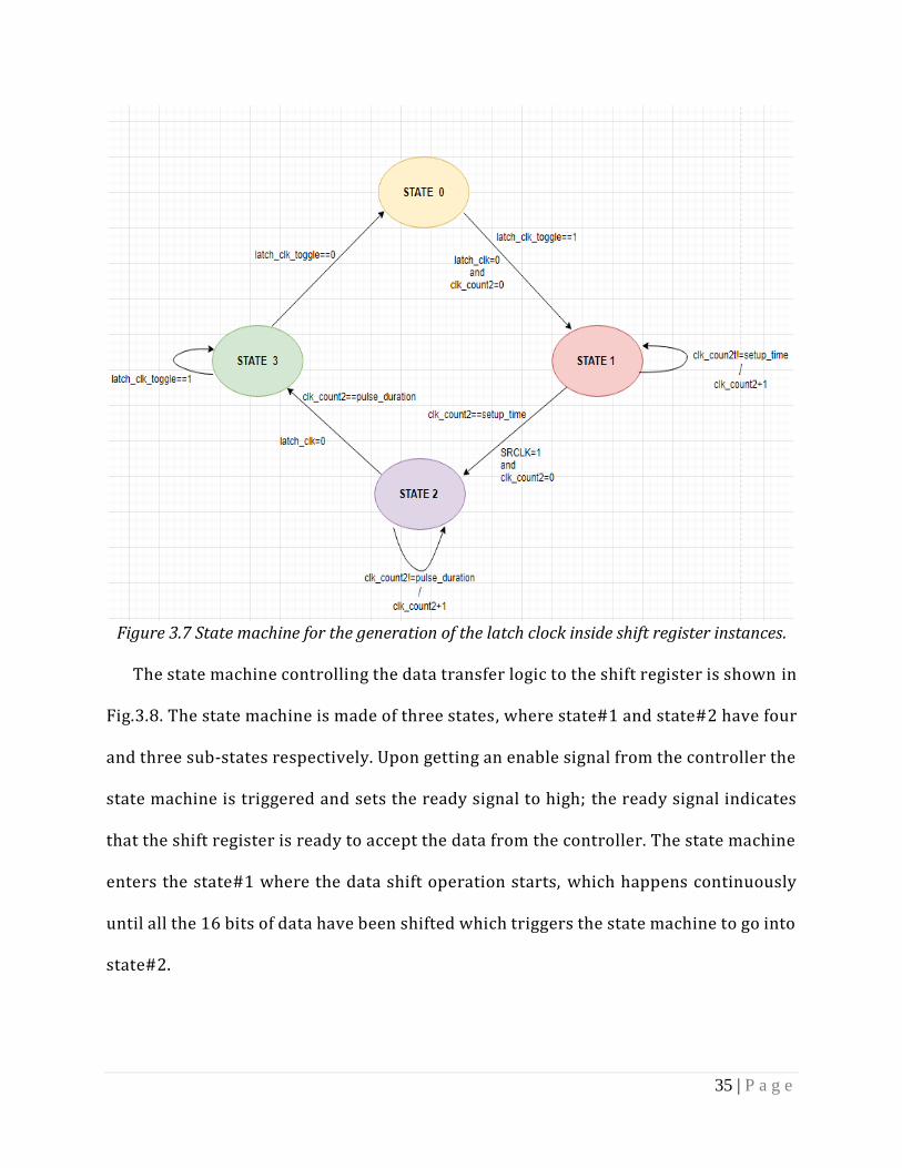
3.7 State machine for the generation of the latch clock inside
shift register instances . . . . . . . . 35
3.8 State machine for controlling the generation of data clock toggle and

ix | P a g e
latch clock toggle and for the transfer of data to the shift register . . . 36
3.9 A timing diagram showing the relationship between row and column latch 38
4.1 2T1C pixel circuit with the uLED and IGZO TFTs . . . 40
4.2 Physical layout of a monochrome pixel circuit using 4µm design rules . 40
4.3 Parasitic elements in a monochrome pixel circuit . . . . 41
4.4 A voltage divider circuit between the storage capacitor and the
driver transistor overlap capacitances . . . . . 42
4.5 Row signal connected to the gate to source capacitance of the pass
transistor . . . . . . . . . 43
4.6 Transient response of the pixel circuit with the ratio of storage cap to
the overlap cap being 1 . . . . . . . 44
4.7 Transient response of the pixel circuit to the ratio of Cst/Cov=33 . 46
4.8 Storage Capacitor node voltage going below 0V due to charge
re-distribution . . . . . . . . 47
4.9 Simulation results for sweeping the storage capacitor from 0.5pF to 2.0pF . 48
4.10 Simulation results for storage capacitor value of 1pF for a target
current value of 50 and 20µA . . . . . . 49
4.11 A ladder network of resistances and capacitances on a row line for a
10x10 pixel array . . . . . . . . 52
4.12 Results of the row-line RC delay(X) simulations for all the matrices with
a row line resistance of 10Ω and an overlap capacitance of 0.8pF . . 53
4.13 Results of the column-line RC delay(Y) simulations for all the matrices
with a row line resistance of 3.7Ω and an overlap capacitance of 0.5pF . . 54

x | P a g e
4.14 A circuit to simulate the change in the current flowing across a uLED
due a small change in the power supply voltage . . . . 56
4.15 The impact of change in Vdd due to the resistances outside the pixel circuit
on the drain current . . . . . . . . 57
4.16 Load Line plot of the driver transistor output characteristics and the uLED
load connected . . . . . . . . 57
4.17 A representation of the circuit used to analyze the effects of voltage drop
due to power and ground line resistances . . . . . 58
4.18 The difference in the minimum and maximum current values with the
monochrome design where Rvdd=10 Ω and Rgnd=3.7 Ω . . . 59
4.19 The difference in the minimum and maximum current values with the
monochrome design where Rvdd=3.7 Ω and Rgnd=3.7 Ω . . . 60
4.20 A surface plot showing the value of current flowing through a pixel circuit
depending upon their respective placement on the grid . . . 61
4.21 Physical layout of a RGB pixel circuit using 4µm design rules . . 62
4.22 A cross-section representation of a driver TFT in a RGB pixel physical
layout . . . . . . . . . 63
4.23 Parasitic elements in a RGB pixel circuit . . . . . 63
5.1 A conventional Flip Chip bonding process . . . . . 67
5.2 A conventional ACF bonding process . . . . . 68
5.3 A Bottom Gate TFT of 2µm channel length with ALD alumina
stable at 200oC . . . . . . . . 68
5.4 Impact bearing capacity versus the bonding temperature for ACF bonding . 68

xi | P a g e
5.5 A test PCB with 50 electrodes arranged in a serpentine arrangement
placed on opposite sides . . . . . . . 69
5.6 Side view of the via up/down chain between the metal on glass
and the PCB . . . . . . . . . 70
5.7 PCB and glass bonded together by an ACF bonding scheme . . 70
5.8 Resistance vs number of vias on the test PCB . . . . . 71
5.9 A tiled arrangement of uLED backplane to realize a big display . . 72
5.10 A four point probe set-up done to measure the line resistance and
contact resistance of the wrap around electrodes . . . . 72
5.11 A resistance value of 0.6Ω for a total of 1800µm length wire . . . 73
5.12 Total resistance for different contact pad lengths . . . . 74
xii | P a g e
List of Tables
1.0 Timing, array size and brightness requirements for the uLED backplane . 21
2.0 The pixel charging time (Z) for different values of storage capacitor at two
target currents and the voltage drop due to charge re-distribution for different
values of storage capacitor . . . . . . . . 50
3.0 Resistance and Capacitance values for the row, column, power and ground
signals per pixel in a monochrome pixel design . . . . . 51
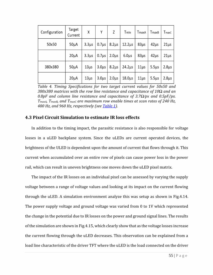
4.0 Timing Specifications for two target current values for 50x50 and
380x380 matrices with the row line resistance and capacitance of 10Ω and
an 0.8pF and column line resistance and capacitance of 3.7Ω and 0.5pF.
TmaxA represents a refresh rate/brightness of 30Hz/3 bit,
TmaxB represents 4bit/30Hz and TmaxC represents 4bit/60Hz . . . . 55
5.0 Resistance and Capacitance values for the row, column, power
and ground signals per pixel in a RGB pixel design . . . . . . 64
6.0 Timing Specifications for two target current values for 50x50 and
380x380 matrices with the row line resistance and capacitance of 10Ω and
an 0.8pF and column line resistance and capacitance of 3.7Ω and 0.5pF
TmaxA represents a refresh rate/brightness of 30Hz/3 bit,
TmaxB represents 4bit/30Hz and TmaxC represents 4bit/60Hz . . . 65
xiii | P a g e
ABSTRACT
Display technologies have evolved from the bulky Cathode Ray Tube based displays to the
latest lightweight and low power micro-Led (uLED) based flat panel displays. A display
system consists of a device technology that either manipulates the incoming light or emits
its own light and a controller circuit to control the behavior of these devices. This system
makes up the backplane of a display technology. uLEDs due to their small size provide higher
resolution and better contrast than all the previous display technologies like the LCDs and
the OLEDs. Backplane system design considerations for a uLED flat panel display is the
primary focus of this work. The uLEDs are arranged in a 2-D matrix on a glass substrate with
each uLED driven by an arrangement of 2 transistor and 1 capacitor that make up a pixel
circuit. Indium Gallium Zinc Oxide TFTs are used as the choice of transistors for this project.
The backplane design considerations are done to support an active matrix of 10x10, 50x50
and 380x380 pixel count in both monochrome and color versions. The behavior of the pixel
circuit is evaluated using existing TFT and uLED electrical device compact models to
determine the optimal value of the storage capacitor needed for the pixel circuit operation
at 30 & 60Hz refresh rates. A model board with shift registers, transistors and LEDs to mimic
the operation of a 10x10 uLED array is made and a FPGA is used to control the operation of
this board. A timing relationship between the row and column data latch is deduced and the
impact of the row-line, column-line RC delay and the pixel transient response time is
evaluated. The impact of IR losses due to the power and ground line resistances are
evaluated with the help monochrome pixel circuit physical layout. A new pixel circuit to
accommodate the RGB pixels is made and care is taken to minimize both the RC delay and IR

xiv | P a g e
losses. Finally, a low contact resistance (0.05Ω-mm2) modular packaging scheme to
electrically bond the two-dimensional array of pixel circuits on glass with the electronics on
the PCB and to reduce RC delay is given.
1 | P a g e
1. Introduction
With the enhancements in network and broadband internet the world is becoming
more connected than ever. Technologies like 5G are enabling applications that have
made access to information very easy and fast. Flat-panel displays (FPDs) play a very
important role in this technological evolution, as they serve as the interface between
humans and the advances in technology that are beneficial to our lives. The insatiable
demand for higher resolution, better contrast and bigger screens has led to tremendous
advancements in FPDs which in turn has led to the development of technologies like
Liquid Crystal Display (LCD), Organic Light emitting Diode (OLED) and more recently
the Micro Light Emitting Diode (uLED). The physics of operation of different FPD
technologies directly influences the various driving schemes used to make them work.
When designing the driver system for a FPD, the controlling logic must interact with the
pixel arrangement to display the desired data.
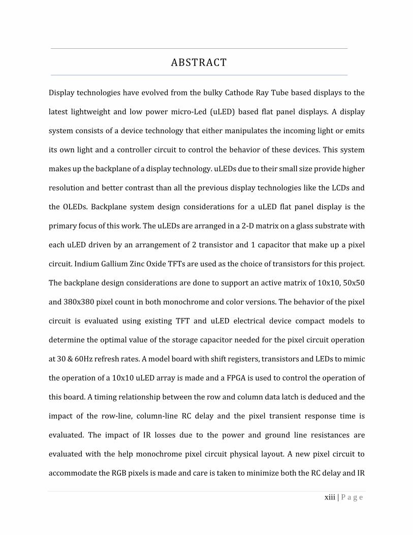
1.1 Working Principle of operation of Flat-panel display technologies:
In order to develop a driving scheme for the FPDs it is important to understand the
principle of their operation. A schematic view of a LCD is shown in Figure 1.1
2 | P a g e
Figure 1.1: Structure of a LCD display [1].
The pixels in a LCD are arranged in a matrix, with TFTs (Thin Film Transistors)
driving each pixel. Such an arrangement is known as an AMLCD (Active Matrix Liquid
Crystal Display) where in the TFTs are used to write and store a charge across a storage
capacitor. This voltage across the storage capacitor, controlled by the TFTs is
responsible for the amount of twist that the LC (Liquid Crystal) produces on the
incoming polarized light. After being subjected to the twist, the twisted polarized light
is then passed to a color filter which is placed perpendicular to the direction of the first
polarizer. The LCDs can be reflective, trans-emissive or trans-reflective, Reflective LCDs
don’t require a backlight and depend upon the ambient light to be viewed while the
trans-emissive screens must have a backlight to them and can be most commonly found
in modern day electronic products like phones and tablets. The trans-reflective screens
have the option of being trans-missive and reflective. LCDs are known as non-emissive
displays as they don’t emit their own light, and require a backlight to illuminate the
display. The most common arrangement of LCs in the LCDs is in the nematic phase, these
3 | P a g e
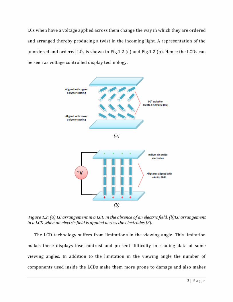
LCs when have a voltage applied across them change the way in which they are ordered
and arranged thereby producing a twist in the incoming light. A representation of the
unordered and ordered LCs is shown in Fig.1.2 (a) and Fig.1.2 (b). Hence the LCDs can
be seen as voltage controlled display technology.
(a)
(b)
Figure 1.2: (a) LC arrangement in a LCD in the absence of an electric field. (b)LC arrangement in a LCD when an electric field is applied across the electrodes [2].
The LCD technology suffers from limitations in the viewing angle. This limitation
makes these displays lose contrast and present difficulty in reading data at some
viewing angles. In addition to the limitation in the viewing angle the number of
components used inside the LCDs make them more prone to damage and also makes
4 | P a g e
these displays bulkier than other technologies. uLED and OLED are both emissive devices
unlike the LCDs and need a current source to drive current through them. These displays
provide a better alternate over LCDs as they are emissive in nature and require fewer
components than the LCDs.
OLEDs (Organic Light Emitting Diodes) are composed of layers of organic material
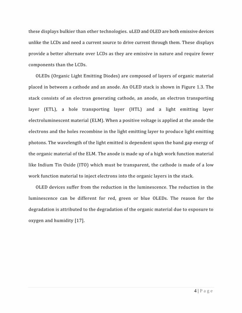
placed in between a cathode and an anode. An OLED stack is shown in Figure 1.3. The
stack consists of an electron generating cathode, an anode, an electron transporting
layer (ETL), a hole transporting layer (HTL) and a light emitting layer
electroluminescent material (ELM). When a positive voltage is applied at the anode the
electrons and the holes recombine in the light emitting layer to produce light emitting
photons. The wavelength of the light emitted is dependent upon the band gap energy of
the organic material of the ELM. The anode is made up of a high work function material
like Indium Tin Oxide (ITO) which must be transparent, the cathode is made of a low
work function material to inject electrons into the organic layers in the stack.
OLED devices suffer from the reduction in the luminescence. The reduction in the
luminescence can be different for red, green or blue OLEDs. The reason for the
degradation is attributed to the degradation of the organic material due to exposure to
oxygen and humidity [17].
5 | P a g e
Figure 1.3: OLED stack [3].
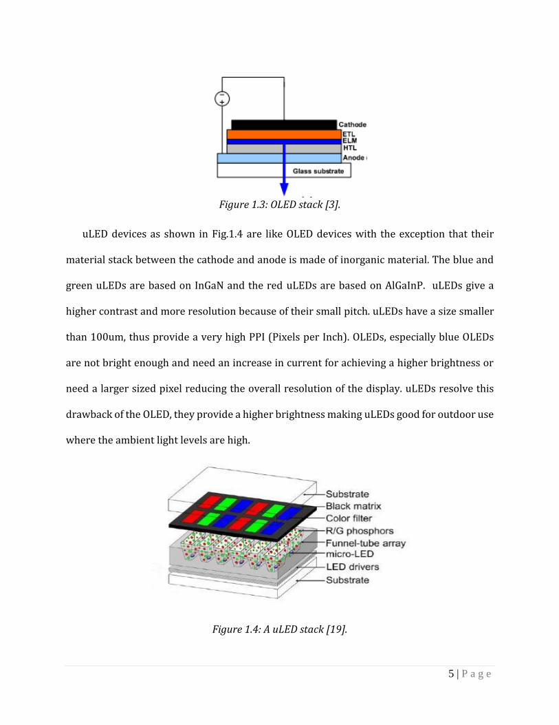
uLED devices as shown in Fig.1.4 are like OLED devices with the exception that their
material stack between the cathode and anode is made of inorganic material. The blue and
green uLEDs are based on InGaN and the red uLEDs are based on AlGaInP. uLEDs give a
higher contrast and more resolution because of their small pitch. uLEDs have a size smaller
than 100um, thus provide a very high PPI (Pixels per Inch). OLEDs, especially blue OLEDs
are not bright enough and need an increase in current for achieving a higher brightness or
need a larger sized pixel reducing the overall resolution of the display. uLEDs resolve this
drawback of the OLED, they provide a higher brightness making uLEDs good for outdoor use
where the ambient light levels are high.
Figure 1.4: A uLED stack [19].
6 | P a g e
1.2 Pixel Addressing Schemes:
FPD resolution is governed by the number of pixels that are present on it. These
pixels can be made of either an emissive or a non-emissive devices arranged in a 2-D
(two dimensional) matrix. In both the cases these pixels need to be addressed to show
the data on the FPD. There are two types of addressing schemes that can be employed
for addressing pixels on an emissive FPD, a passive matrix addressing scheme and an
active matrix addressing scheme.
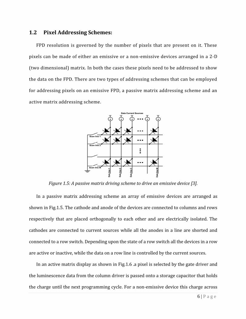
Figure 1.5: A passive matrix driving scheme to drive an emissive device [3].
In a passive matrix addressing scheme an array of emissive devices are arranged as
shown in Fig.1.5. The cathode and anode of the devices are connected to columns and rows
respectively that are placed orthogonally to each other and are electrically isolated. The
cathodes are connected to current sources while all the anodes in a line are shorted and
connected to a row switch. Depending upon the state of a row switch all the devices in a row
are active or inactive, while the data on a row line is controlled by the current sources.
In an active matrix display as shown in Fig.1.6 .a pixel is selected by the gate driver and
the luminescence data from the column driver is passed onto a storage capacitor that holds
the charge until the next programming cycle. For a non-emissive device this charge across
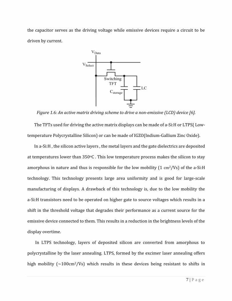
7 | P a g e
the capacitor serves as the driving voltage while emissive devices require a circuit to be
driven by current.
Figure 1.6: An active matrix driving scheme to drive a non-emissive (LCD) device [6].
The TFTs used for driving the active matrix displays can be made of a-Si:H or LTPS( Low-
temperature Polycrystalline Silicon) or can be made of IGZO(Indium-Gallium Zinc Oxide).
In a-Si:H , the silicon active layers , the metal layers and the gate dielectrics are deposited
at temperatures lower than 350oC . This low temperature process makes the silicon to stay
amorphous in nature and thus is responsible for the low mobility (1 cm2/Vs) of the a-Si:H
technology. This technology presents large area uniformity and is good for large-scale
manufacturing of displays. A drawback of this technology is, due to the low mobility the
a-Si:H transistors need to be operated on higher gate to source voltages which results in a
shift in the threshold voltage that degrades their performance as a current source for the
emissive device connected to them. This results in a reduction in the brightness levels of the
display overtime.
In LTPS technology, layers of deposited silicon are converted from amorphous to
polycrystalline by the laser annealing. LTPS, formed by the excimer laser annealing offers
high mobility (~100cm2/Vs) which results in these devices being resistant to shifts in
8 | P a g e
threshold voltages over-time but due to their high cost manufacturing ,large area non-
uniformity and lower yields this technology is not suited for high resolution applications.
1.3 IGZO material for TFTs:
IGZO (Indium Gallium Zinc Oxide) is composed of three metal oxides namely In2O3,
Ga2O3 and ZnO [4]. IGZO is a wide band gap semiconductor (3.2eV) that provides a very low
leakage current in the order of pico-amps. The ionic bonding in the amorphous IGZO provide
for the electron transport through the s- orbital of the metal cations, giving them a high
carrier mobility (~10 cm2/V-s) [4]. IGZO TFTs have good large area uniformity, and are
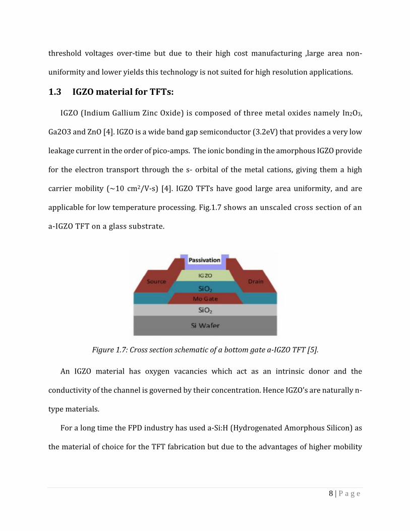
applicable for low temperature processing. Fig.1.7 shows an unscaled cross section of an
a-IGZO TFT on a glass substrate.
Figure 1.7: Cross section schematic of a bottom gate a-IGZO TFT [5].
An IGZO material has oxygen vacancies which act as an intrinsic donor and the
conductivity of the channel is governed by their concentration. Hence IGZO’s are naturally n-
type materials.
For a long time the FPD industry has used a-Si:H (Hydrogenated Amorphous Silicon) as
the material of choice for the TFT fabrication but due to the advantages of higher mobility
9 | P a g e
(~10times) and large area uniformity IGZO TFTs are quickly replacing amorphous silicon
based TFTs in flat panel display technology.
1.4 Flat-Panel Display System:
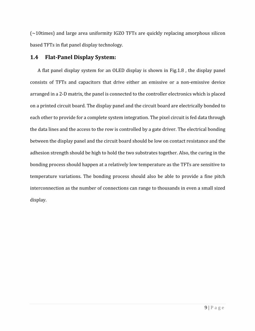
A flat panel display system for an OLED display is shown in Fig.1.8 , the display panel
consists of TFTs and capacitors that drive either an emissive or a non-emissive device
arranged in a 2-D matrix, the panel is connected to the controller electronics which is placed
on a printed circuit board. The display panel and the circuit board are electrically bonded to
each other to provide for a complete system integration. The pixel circuit is fed data through
the data lines and the access to the row is controlled by a gate driver. The electrical bonding
between the display panel and the circuit board should be low on contact resistance and the
adhesion strength should be high to hold the two substrates together. Also, the curing in the
bonding process should happen at a relatively low temperature as the TFTs are sensitive to
temperature variations. The bonding process should also be able to provide a fine pitch
interconnection as the number of connections can range to thousands in even a small sized
display.
10 | P a g e
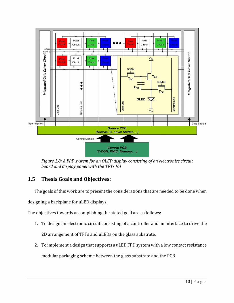
Figure 1.8: A FPD system for an OLED display consisting of an electronics circuit board and display panel with the TFTs [6]
1.5 Thesis Goals and Objectives:
The goals of this work are to present the considerations that are needed to be done when
designing a backplane for uLED displays.
The objectives towards accomplishing the stated goal are as follows:
1. To design an electronic circuit consisting of a controller and an interface to drive the
2D arrangement of TFTs and uLEDs on the glass substrate.
2. To implement a design that supports a uLED FPD system with a low contact resistance
modular packaging scheme between the glass substrate and the PCB.

11 | P a g e
3. To perform circuit simulations using the TFT and uLED model and come up with a
feasible value of the storage capacitor.
4. To assess the impact of delays due to the parasitics offered by the row and column
signal lines on the pixel circuit and to verify that they meet the timing requirements
of the system.
5. To analyze the impact of voltage drops due to the line resistance on the power rails
and to re-design of the circuit based on the results of the analysis.
6. To design the physical layout of a RGB pixel circuit with lower line resistances and
capacitances and fit it in a 200µm pitch.
7. To quantify the backplane performance considering the pixel transient response, row
and column RC delay, and IR voltage losses.
1.6 Chapter Organization
Chapter 1 has described the principle of operation of flat panel displays and the
addressing schemes used to drive them. The goals and objectives for this thesis have also
been outline in this chapter.
Chapter 2 discusses the elements that are used in the design of a display backplane
system and their considerations when used for making a uLED backplane system. This
chapter describes the uLED and the IGZO TFT model.
Chapter 3 describes the use of a model board to develop the FPGA code for a 10x10 pixel
circuit array. A timing relationship between the row and column latch clock is given and its
dependence on the row-line RC delay, column-line RC delay and the transient response time
is shown.

12 | P a g e
Chapter 4 presents the circuit simulations using the uLED and IGZO model to determine
an optimal value of the storage capacitor needed in the design. The impact of line parasitic
elements on the performance of the pixel circuit array are shown. Simulations of row and
column RC delay and the IR losses due to the power and ground line resistances are shown.
Finally, a new pixel circuit design accommodating the signal line constraints for the RGB
pixel circuit is given,
Chapter 5 discusses the packaging scheme for doing the bonding between the glass
substrate and the PCB and the electronic circuitry required to drive the pixel circuit array on
glass.
Chapter 6 concludes this thesis and provides conclusions from this work and presents
the scope of improvement.
13 | P a g e
2. Design Considerations for a uLED display backplane
A uLED backplane for an active matrix display technology consists of a 2-D pixel circuit
arrangement on top of a substrate connected to the row and column drivers which drive the
uLEDs and a control circuitry on a PCB (printed circuit board) that has the logic elements for
filling the row and column registers with data containing the image and brightness
information to be displayed. The PCB and the backplane must have an electrical signal
interface. The choice of TFTs, their dimensions, the delay requirements, the choice of
controller and the interface between the controller and the substrate, are governed by the
timing requirements of the display that are intern dependent upon the refresh rate and the
brightness level specified for the display. Brightness of the uLEDs can be controlled by either
using a PWM (pulse width modulation) scheme or by current modulation across the uLED.
The PWM scheme provides for a simpler design as unlike the current modulation scheme a
digital to analog (D/A) converter is not required. A refresh rate is defined as the number of
times per second a display device updates the image, the brightness of a display is defined
as the perceived intensity of the light from a display. This chapter will discuss the details of
these components and their impact on the design of a uLED display backplane.
2.1 Pixel Circuits
The simplest form of a driving circuit is a 2 Transistor 1 Capacitor (2T1C) combination
as shown in Fig.2.1. T1 is known as the pass gate responsible for passing the data from the
data line (column) to T2 and the storage capacitor (Cst) when a row is selected. TFT T1 is
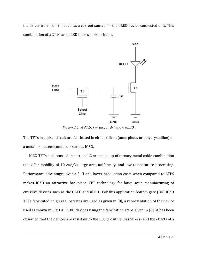
14 | P a g e
the driver transistor that acts as a current source for the uLED device connected to it. This
combination of a 2T1C and uLED makes a pixel circuit.
Figure 2.1: A 2T1C circuit for driving a uLED.
The TFTs in a pixel circuit are fabricated in either silicon (amorphous or polycrystalline) or
a metal-oxide semiconductor such as IGZO.
IGZO TFTs as discussed in section 1.2 are made up of ternary metal oxide combination
that offer mobility of 10 cm2/Vs large area uniformity, and low temperature processing.
Performance advantages over a-Si:H and lower production costs when compared to LTPS
makes IGZO an attractive backplane TFT technology for large scale manufacturing of
emissive devices such as the OLED and uLED. For this application bottom gate (BG) IGZO
TFTs fabricated on glass substrates are used as given in [8], a representation of the device
used is shown in Fig.1.4. In BG devices using the fabrication steps given in [8], it has been
observed that the devices are resistant to the PBS (Positive Bias Stress) and the effects of a
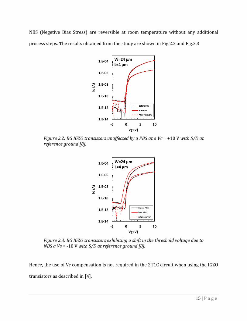
15 | P a g e
NBS (Negetive Bias Stress) are reversible at room temperature without any additional
process steps. The results obtained from the study are shown in Fig.2.2 and Fig.2.3
Figure 2.2: BG IGZO transistors unaffected by a PBS at a VG = +10 V with S/D at reference ground [8].
Figure 2.3: BG IGZO transistors exhibiting a shift in the threshold voltage due to NBS a VG = -10 V with S/D at reference ground [8].
Hence, the use of VT compensation is not required in the 2T1C circuit when using the IGZO
transistors as described in [4].
16 | P a g e
2.2 TFT and uLED model
To use the IGZO TFTs in a 2T1C pixel circuit with uLEDs, it is important to accurately
model the behavior of both the IGZO TFT and the uLED. Circuit simulations using the
representative device models and parasitic elements from the physical layout provide
insight into how the circuit will respond to the application of row and column signals. This
will establish pixel design parameters such as the transistor dimensions, requirements of
line resistances and the size of the storage capacitor that supports the correct operation of
the circuit.
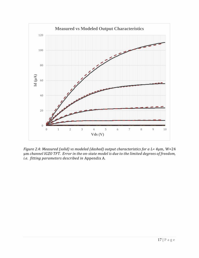
2.2.1 TFT compact Model
An on-state model for IGZO TFTs developed by Hirschman et al [9] and was extended
by Rubio [10] to include the off state behavior and intermediate transition region;
details are provided in the Appendix A. Overlays of the measured and simulated Id-Vg
transfer characteristics and Id-Vds output characteristics of an L=4 µm and W=24 µm
TFT are shown in Fig.2.4 and Fig.2.5, respectively. These length and widths correspond
to the actual TFT dimensions used in the pixel circuit design.
17 | P a g e
Figure 2.4: Measured (solid) vs modeled (dashed) output characteristics for a L= 4µm, W=24 µm channel IGZO TFT. Error in the on-state model is due to the limited degrees of freedom, i.e. fitting parameters described in Appendix A.
0
20
40
60
80
100
120
0 1 2 3 4 5 6 7 8 9 10
Id (
µA
)
Vds (V)
Measured vs Modeled Output Characteristics
18 | P a g e
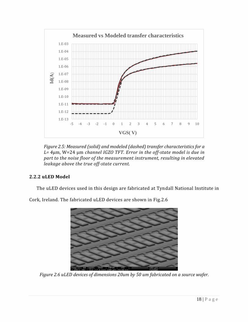
Figure 2.5: Measured (solid) and modeled (dashed) transfer characteristics for a L= 4µm, W=24 µm channel IGZO TFT. Error in the off-state model is due in part to the noise floor of the measurement instrument, resulting in elevated leakage above the true off-state current.
2.2.2 uLED Model
The uLED devices used in this design are fabricated at Tyndall National Institute in
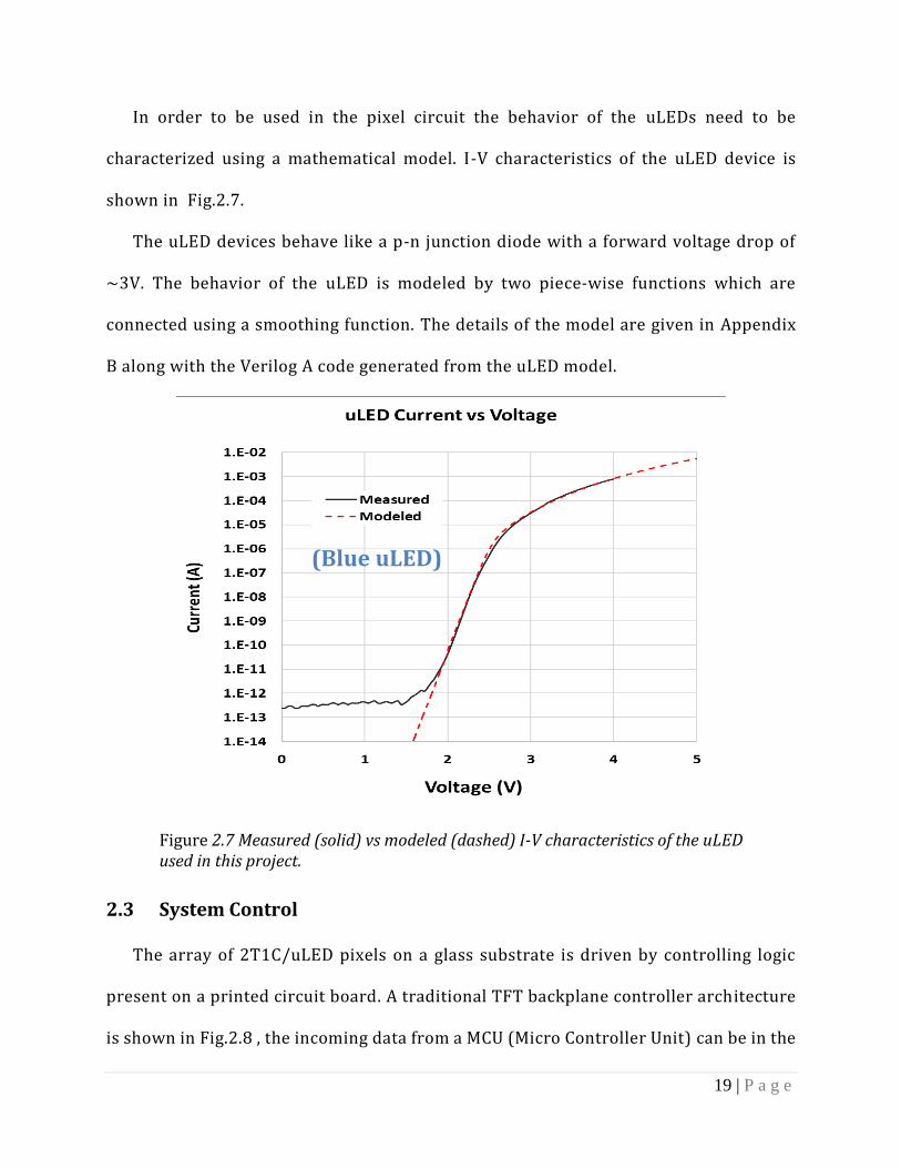
Cork, Ireland. The fabricated uLED devices are shown in Fig.2.6
Figure 2.6 uLED devices of dimensions 20um by 50 um fabricated on a source wafer.
1.E-13
1.E-12
1.E-11
1.E-10
1.E-09
1.E-08
1.E-07
1.E-06
1.E-05
1.E-04
1.E-03
-5 -4 -3 -2 -1 0 1 2 3 4 5 6 7 8 9 10
Id(A
)
VGS( V)
Measured vs Modeled transfer characteristics
19 | P a g e
In order to be used in the pixel circuit the behavior of the uLEDs need to be
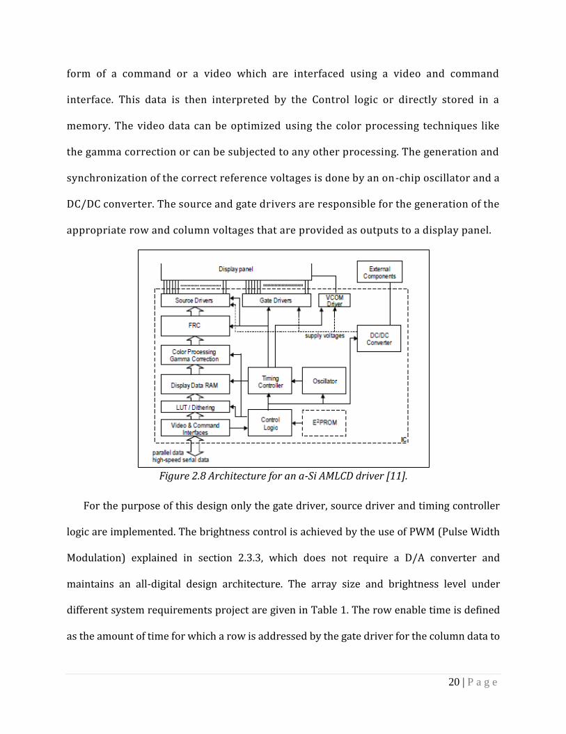
characterized using a mathematical model. I-V characteristics of the uLED device is
shown in Fig.2.7.
The uLED devices behave like a p-n junction diode with a forward voltage drop of
~3V. The behavior of the uLED is modeled by two piece-wise functions which are
connected using a smoothing function. The details of the model are given in Appendix
B along with the Verilog A code generated from the uLED model.
Figure 2.7 Measured (solid) vs modeled (dashed) I-V characteristics of the uLED used in this project.
2.3 System Control
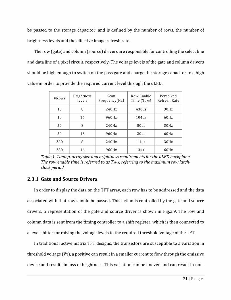
The array of 2T1C/uLED pixels on a glass substrate is driven by controlling logic
present on a printed circuit board. A traditional TFT backplane controller architecture
is shown in Fig.2.8 , the incoming data from a MCU (Micro Controller Unit) can be in the
(Blue uLED)
20 | P a g e
form of a command or a video which are interfaced using a video and command
interface. This data is then interpreted by the Control logic or directly stored in a
memory. The video data can be optimized using the color processing techniques like
the gamma correction or can be subjected to any other processing. The generation and
synchronization of the correct reference voltages is done by an on-chip oscillator and a
DC/DC converter. The source and gate drivers are responsible for the generation of the
appropriate row and column voltages that are provided as outputs to a display panel.
Figure 2.8 Architecture for an a-Si AMLCD driver [11].
For the purpose of this design only the gate driver, source driver and timing controller
logic are implemented. The brightness control is achieved by the use of PWM (Pulse Width
Modulation) explained in section 2.3.3, which does not require a D/A converter and
maintains an all-digital design architecture. The array size and brightness level under
different system requirements project are given in Table 1. The row enable time is defined
as the amount of time for which a row is addressed by the gate driver for the column data to
21 | P a g e
be passed to the storage capacitor, and is defined by the number of rows, the number of
brightness levels and the effective image refresh rate.
The row (gate) and column (source) drivers are responsible for controlling the select line
and data line of a pixel circuit, respectively. The voltage levels of the gate and column drivers
should be high enough to switch on the pass gate and charge the storage capacitor to a high
value in order to provide the required current level through the uLED.
#Rows Brightness
levels Scan
Frequency(Hz) Row Enable Time (TMAX)
Perceived Refresh Rate
10 8 240Hz 430µs 30Hz
10 16 960Hz 104µs 60Hz
50 8 240Hz 80µs 30Hz
50 16 960Hz 20µs 60Hz
380 8 240Hz 11µs 30Hz
380 16 960Hz 3µs 60Hz
Table 1. Timing, array size and brightness requirements for the uLED backplane. The row enable time is referred to as TMAX, referring to the maximum row latch-clock period.
2.3.1 Gate and Source Drivers
In order to display the data on the TFT array, each row has to be addressed and the data
associated with that row should be passed. This action is controlled by the gate and source
drivers, a representation of the gate and source driver is shown in Fig.2.9. The row and
column data is sent from the timing controller to a shift register, which is then connected to
a level shifter for raising the voltage levels to the required threshold voltage of the TFT.
In traditional active matrix TFT designs, the transistors are susceptible to a variation in
threshold voltage (VT), a positive can result in a smaller current to flow through the emissive
device and results in loss of brightness. This variation can be uneven and can result in non-
22 | P a g e
uniform brightness on a FPD. Buffer circuits are used to mitigate this variation in the
threshold shift by being implemented at the outputs of the source and gate drivers of the
shift register circuits, a source follower type analog buffer circuit is the most common type
of buffer circuit used for this purpose. The use of analog buffers is common when the
brightness levels are current modulated, but in a PWM (discussed in Sec2.3) scheme digital
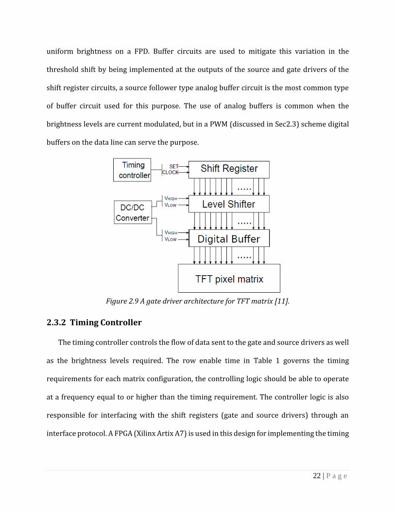
buffers on the data line can serve the purpose.
Figure 2.9 A gate driver architecture for TFT matrix [11].
2.3.2 Timing Controller
The timing controller controls the flow of data sent to the gate and source drivers as well
as the brightness levels required. The row enable time in Table 1 governs the timing
requirements for each matrix configuration, the controlling logic should be able to operate
at a frequency equal to or higher than the timing requirement. The controller logic is also
responsible for interfacing with the shift registers (gate and source drivers) through an
interface protocol. A FPGA (Xilinx Artix A7) is used in this design for implementing the timing

23 | P a g e
controller, the maximum internal clock frequency of the device is 450 MHz [16] which can
easily meet the most stringent timing requirements in Table1 (380x380 color).
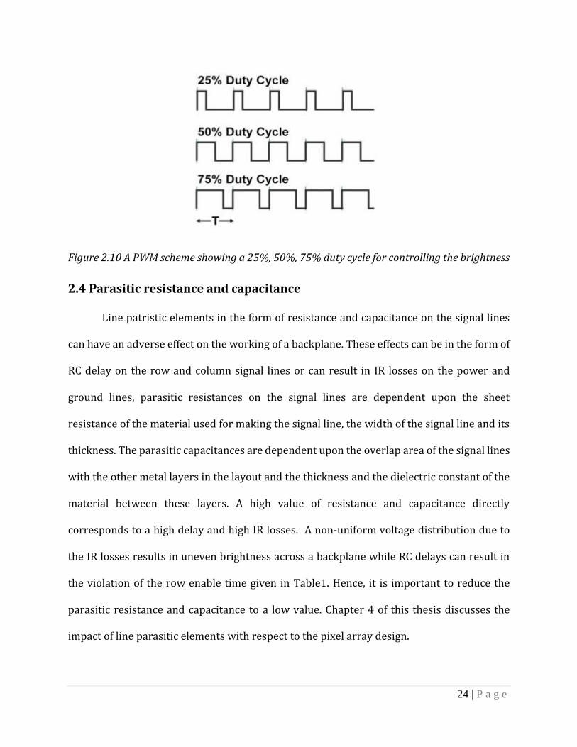
2.3.3 PWM for pixel brightness control
The brightness of a display can be controlled by using a PWM (Pulse Width Modulation)
scheme in which the duty cycle of the data is varied to realize different brightness levels. The
brightness requirements of the display are specified in terms of the number of bits(y), e.g.
3-bit or 4-bit, which means that there are 2y number of brightness levels. If the data being
sent to a pixel is high for all the 2y number of cycles then a 100% brightness is achieved,
while if the data signal is on for only one out of all the 2y number of cycles then the least
amount of brightness level is achieved. All the pixels in an array are needed to be addressed
2y number of times within an effective refresh cycle. For example in a 3bit/30Hz
brightness/refresh cycle, all the pixels are required to be addressed 8 times within
1
30=33.33ms. Hence, the brightness of a pixel is dependent upon the number of cycles the data
value is 1 on a pixel out of the total number of brightness cycles. Refer to Appendix C for an
example of PWM encoded data scheme. Timing relationships for various arrangements are
shown in Table 1. The scan frequency and number of brightness levels establish the
perceived refresh rate.
24 | P a g e
Figure 2.10 A PWM scheme showing a 25%, 50%, 75% duty cycle for controlling the brightness
2.4 Parasitic resistance and capacitance
Line patristic elements in the form of resistance and capacitance on the signal lines
can have an adverse effect on the working of a backplane. These effects can be in the form of
RC delay on the row and column signal lines or can result in IR losses on the power and
ground lines, parasitic resistances on the signal lines are dependent upon the sheet
resistance of the material used for making the signal line, the width of the signal line and its
thickness. The parasitic capacitances are dependent upon the overlap area of the signal lines
with the other metal layers in the layout and the thickness and the dielectric constant of the
material between these layers. A high value of resistance and capacitance directly
corresponds to a high delay and high IR losses. A non-uniform voltage distribution due to
the IR losses results in uneven brightness across a backplane while RC delays can result in
the violation of the row enable time given in Table1. Hence, it is important to reduce the
parasitic resistance and capacitance to a low value. Chapter 4 of this thesis discusses the
impact of line parasitic elements with respect to the pixel array design.
25 | P a g e
2.5 Summary
This chapter covers the major design considerations for the parts used in the
development of a uLED backplane. The TFT model was described and the characteristics of
a 4µm channel length TFT was shown, this TFT will be used in the pixel circuit as the pass
gate and the driver transistor. The mathematical model of the uLED was also given. The Tmax
and brightness values for different perceived refresh rates for different number of rows in a
pixel matrix were given, this Tmax serves as the matrix of comparison for the delay value
calculations done later in this work. The controlling circuitry was introduced which drives
the pixel circuit on glass, and the impact of line parasitic elements on the pixel circuit was
introduced. In the next chapter the design of a FPGA code for a 10x10 model board will be
shown and a relationship between the row latch and column latch will be given.

26 | P a g e
III. Design of the FPGA code for the model board
The last chapter discussed the various elements needed for the design of a uLED
backplane. This chapter will show the results of the implementation using those design
elements. A model board which mimics the actual 2T1C arrangement on glass for the
development of the FPGA code is shown. The FPGA code written for this model board and
the findings from this experiment will be given in this chapter.
3.1 Model Board
In order to develop the FPGA code, a model board with a 2T1C circuit was made. The
board shown in Fig. 3.0 has LEDs arranged in a 10x10, 2-D matrix each controlled by two
power transistors with a gate threshold voltage of 1V. The device input capacitance serves
as the storage capacitor. The row line data is controlled by the two the shift registers at the
bottom, while the column data line is controlled by the two shift registers on the right. The
shift registers used in the design are Texas Instrument’s 8 bit CD74HC595N, the working of
these shift registers is shown in Figure 3.1.
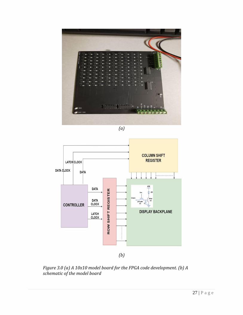
27 | P a g e
(a)
(b)
Figure 3.0 (a) A 10x10 model board for the FPGA code development. (b) A schematic of the model board
28 | P a g e
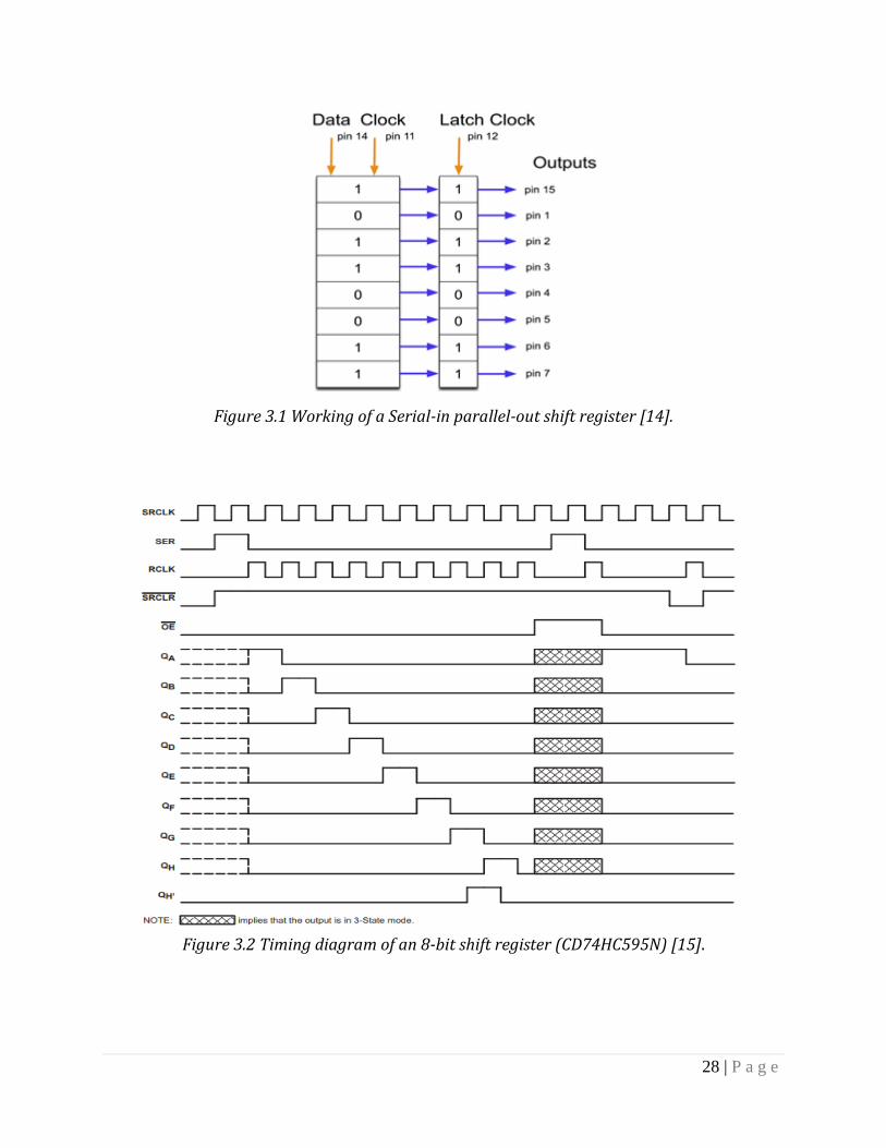
Figure 3.1 Working of a Serial-in parallel-out shift register [14].
Figure 3.2 Timing diagram of an 8-bit shift register (CD74HC595N) [15].

29 | P a g e
The serial-in parallel out behavior of the shift register shown in Fig.3.1, shows the data
being fed in serially on the rising edge of the data clock (SRCLK) to the shift register and
when the latch pin is enabled on the latch clock (RCLK), the data is transferred to the output
pins via a latch register. As the latch clock goes down the transfer of the data to the latch pin
seizes and the data is available on the output pins until the next latch clock is applied. The
CD74HC595 shift register gives 5V voltage at its output pins, which is greater than the
threshold voltage of the transistors connected in the model board hence is able to turn them
on. Two of these shift registers are used in cascaded manner for the row data and other two
cascaded for the column data, a total of 256 LEDs can be addressed using this scheme. Since
the board is populated with 100 LEDs, the last 6 bits of both the row and column cascaded
shift registers are unused. The timing diagram of a single 8-bit shift register is shown in
Fig.3.2. This arrangement will be used for the actual TFT backplane, as more shift registers
can be cascaded to address the 50x50 and 380x380 matrices.
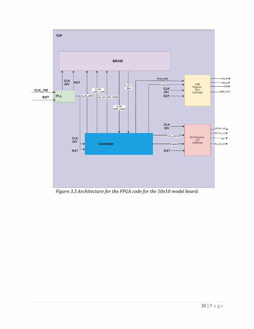
3.2 FPGA Code development
The model board serves as a test platform to develop the FPGA code to be used in the
final design. The final design will need the FPGA to interface with the shift registers to drive
the rows and column data, hence the code developed for the model board will be usable for
the final design. The development platform used for this design is a Digilent Nexus A7
development board having Xillinx Atrix A-7 FPGA.
The high level architecture of the code is shown in Fig. 3.3. The code consists of five main
blocks which are two shift register blocks that control the data transfer to the row and
column driver shift registers, a controller block that interfaces with a block ram (BRAM)
which is an on chip memory in the FPGA to fetch the data and send it to the respective shift
30 | P a g e
register. A Phase Locked Loop (PLL) block for deriving the required frequency of operation
for the controller. The description of each of the block is given in this section and the code is
attached in Appendix C section of this thesis.
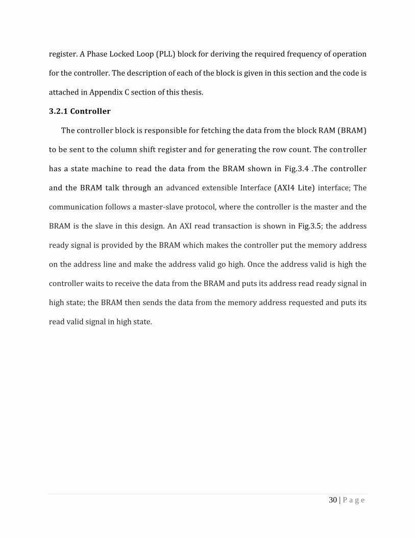
3.2.1 Controller
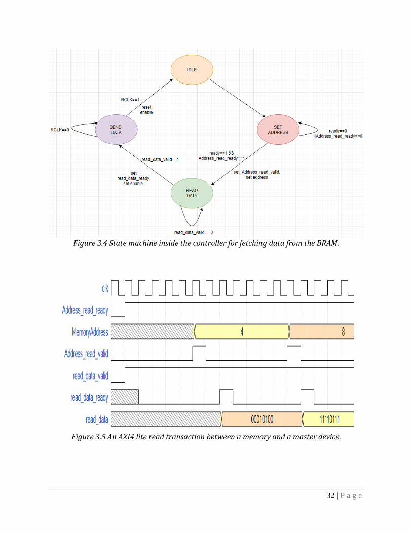
The controller block is responsible for fetching the data from the block RAM (BRAM)
to be sent to the column shift register and for generating the row count. The con troller
has a state machine to read the data from the BRAM shown in Fig.3.4 .The controller
and the BRAM talk through an advanced extensible Interface (AXI4 Lite) interface; The
communication follows a master-slave protocol, where the controller is the master and the
BRAM is the slave in this design. An AXI read transaction is shown in Fig.3.5; the address
ready signal is provided by the BRAM which makes the controller put the memory address
on the address line and make the address valid go high. Once the address valid is high the
controller waits to receive the data from the BRAM and puts its address read ready signal in
high state; the BRAM then sends the data from the memory address requested and puts its
read valid signal in high state.
31 | P a g e
Figure 3.3 Architecture for the FPGA code for the 10x10 model board.
32 | P a g e
Figure 3.4 State machine inside the controller for fetching data from the BRAM.
Figure 3.5 An AXI4 lite read transaction between a memory and a master device.

33 | P a g e
In addition to the address_read_ready and read_data_ready, the controller also uses the
feedback signals from the shift registers. When the shift registers are ready to accept the
data, the state machine of the controller is initiated. When the shift register is done sending
the data, the state machine goes back to the idle state.
3.2.2 Shift register row and column controller
The design makes use of two instances of the shift register, one for driving the row
and the other for driving the columns. The shift registers receive the derived clock and
reset from the PLL, and an enable signal from the controller to start the data t ransfer.
Both the row and the column instances take in 16-bit data from the controller to send
to the two 8-bit shift registers which are cascaded to control the rows and columns. The
row and column shift register instances each consist of two state machines, one for
generating a data clock and the other for generating the latch clock. As discussed in the
last chapter, the data is transferred through the shift registers on each rising edge of
the data clock, and then gets latched and available on the rising edge of the latch-clock.
The state machines for the generation of the data clock and the latch clock are shown
in Fig. 3.6 and Fig.3.7, respectively. The column data is fed from the BRAM, while the
row is generated as a one-hot counter (only 1 bit is high at a time in the entire data
packet) from the controller logic. The memory is initialized with data by using a
Memory Initialization File (.mif) that is generated using a python code, the brightness
control of the LEDs is done by a PWM scheme which is implemented in the data scheme
of the .mif which is attached in the Appendix C section of this thesis.
In this implementation there are two shift registers in cascade for both the row and
the columns, hence 16 data clock cycles are required to transfer the data to the shift
34 | P a g e
registers with each clock transferring 1 bit per clock cycle. After the completion of the
16 data clock cycles the latch clock is enabled which transfers the data to the output
pins of the shift register.
Figure 3.6 State machine for the generation of the data clock inside shift register instances.
For this implementation, the PLL is fed an input clock frequency of 100MHz which then
internally divides the input clock to provide the 5MHz system clock. The PLL also generates
a reset signal for the system.
35 | P a g e
Figure 3.7 State machine for the generation of the latch clock inside shift register instances.
The state machine controlling the data transfer logic to the shift register is shown in
Fig.3.8. The state machine is made of three states, where state#1 and state#2 have four
and three sub-states respectively. Upon getting an enable signal from the controller the
state machine is triggered and sets the ready signal to high; the ready signal indicates
that the shift register is ready to accept the data from the controller. The state machine
enters the state#1 where the data shift operation starts, which happens continuously
until all the 16 bits of data have been shifted which triggers the state machine to go into
state#2.
36 | P a g e
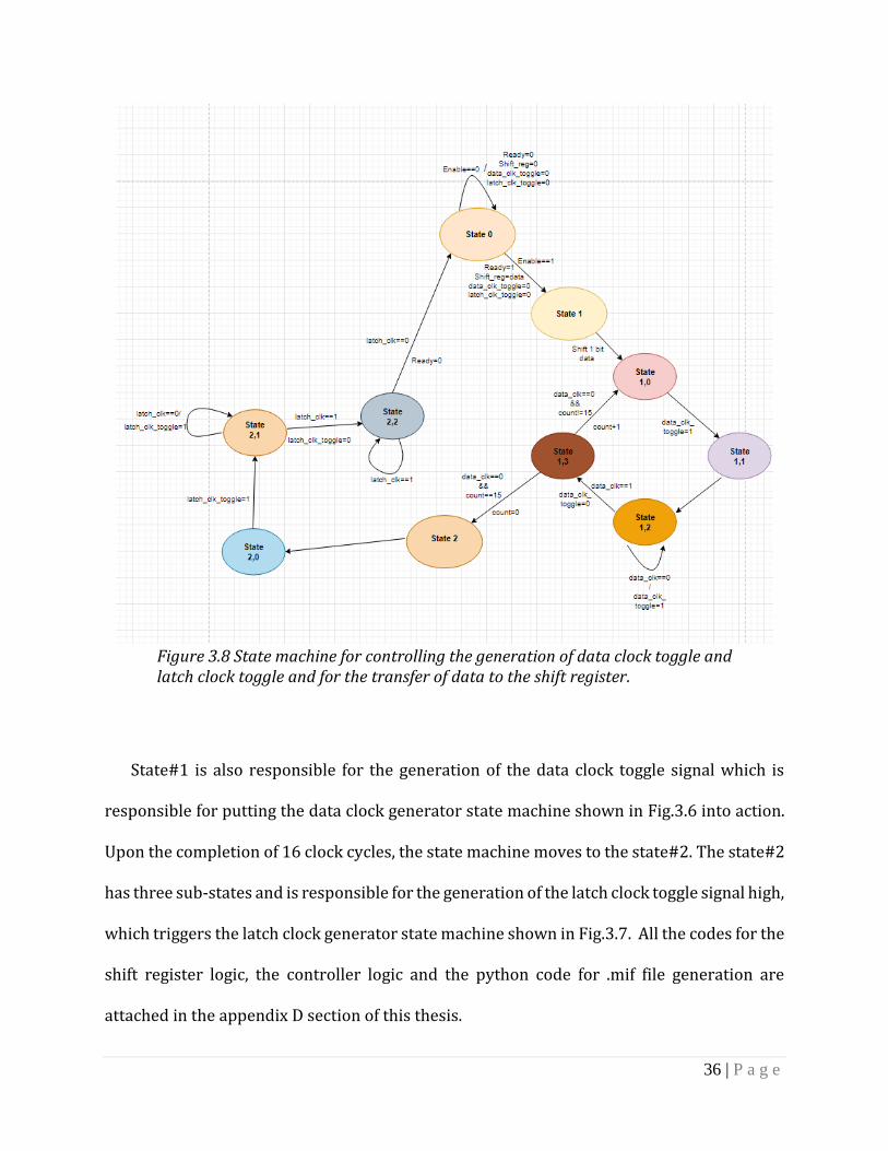
Figure 3.8 State machine for controlling the generation of data clock toggle and latch clock toggle and for the transfer of data to the shift register.
State#1 is also responsible for the generation of the data clock toggle signal which is
responsible for putting the data clock generator state machine shown in Fig.3.6 into action.
Upon the completion of 16 clock cycles, the state machine moves to the state#2. The state#2
has three sub-states and is responsible for the generation of the latch clock toggle signal high,
which triggers the latch clock generator state machine shown in Fig.3.7. All the codes for the
shift register logic, the controller logic and the python code for .mif file generation are
attached in the appendix D section of this thesis.

37 | P a g e
3.3 Row and Column timing
The row and column latching behavior is an important conclusion that was drawn by
using the model board. The column latching should always succeed the data latching as if the
row latch precedes the column latch a wrong data is latched on the preceding row. The
amount of skew between the column latch and the row latch is determined by the row line
RC delay which is the amount of it takes for the row signal to reach the last column in a
particular matrix specification . A relationship between the row and column latch signal is
shown in Fig.3.9. Time “X” represents the hold time, which must be greater than the worst-
case (last pixel) row-line RC delay to the pass gate. This is the “row head start” to ensure that
the present row latches correctly. Time “Y” is the setup time due to the column-line RC delay,
which represents the amount of time it takes for the column line signal to reach the pixel in
the last row. Time “Z” represents the delay of the pass-gate (R = channel resistance) passing
charge to the driver (C = storage capacitor + driver input capacitance). This is the time
needed to get storage capacitor up to the required voltage corresponding to a target current.
Together these three parameters form the minimum latch clock period (Tmin) which can be
quantified as below:
Minimum latch-clock period: Tmin = X+Y+Z
The minimum latch-clock period (Tmin) should be less than the row enable time (Tmax) given
in Table1 .

38 | P a g e
Figure 3.9. Timing diagram showing the relationship between row and column latch-clock signals.
3.4 Summary
The experiments and analysis shown in this chapter are a precursor to the final
integration of the uLED backplane. The FPGA code written for the model board is usable in
the final 10x10 matrix fabricated on glass as well as the design can be extended for the 50x50
and 380x380 resolution by changing the clock timings and using more number of shift
registers. A relation to estimate the skew in between the row and column latch signals and
the its governing parameters were introduced.
In the next chapter, circuit simulations will be done to determine the value of the storage
capacitor required for this project. The impact of parasitic elements in the form resistances
and capacitances will be analyzed as well and strategies to reduce their adverse impact will
be given. The values of X, Y, Z will also be evaluated for different configurations and the
impact of these timings due to the parasitic elements will be evaluated.
39 | P a g e
IV. Pixel Design Considerations
Parasitic elements in the form of resistance and capacitance in a pixel circuit have an
impact on the timing and power requirements of the uLED backplane system. The row signal
line, column signal line, the power rail of the circuit have inherent resistances and
capacitances. These elements must be taken into consideration to determine the values of
row-line RC delay and column-line RC delay.
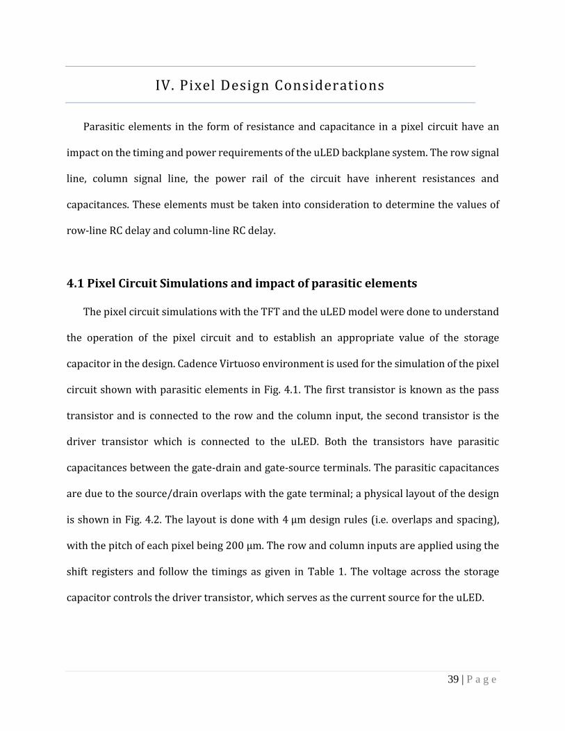
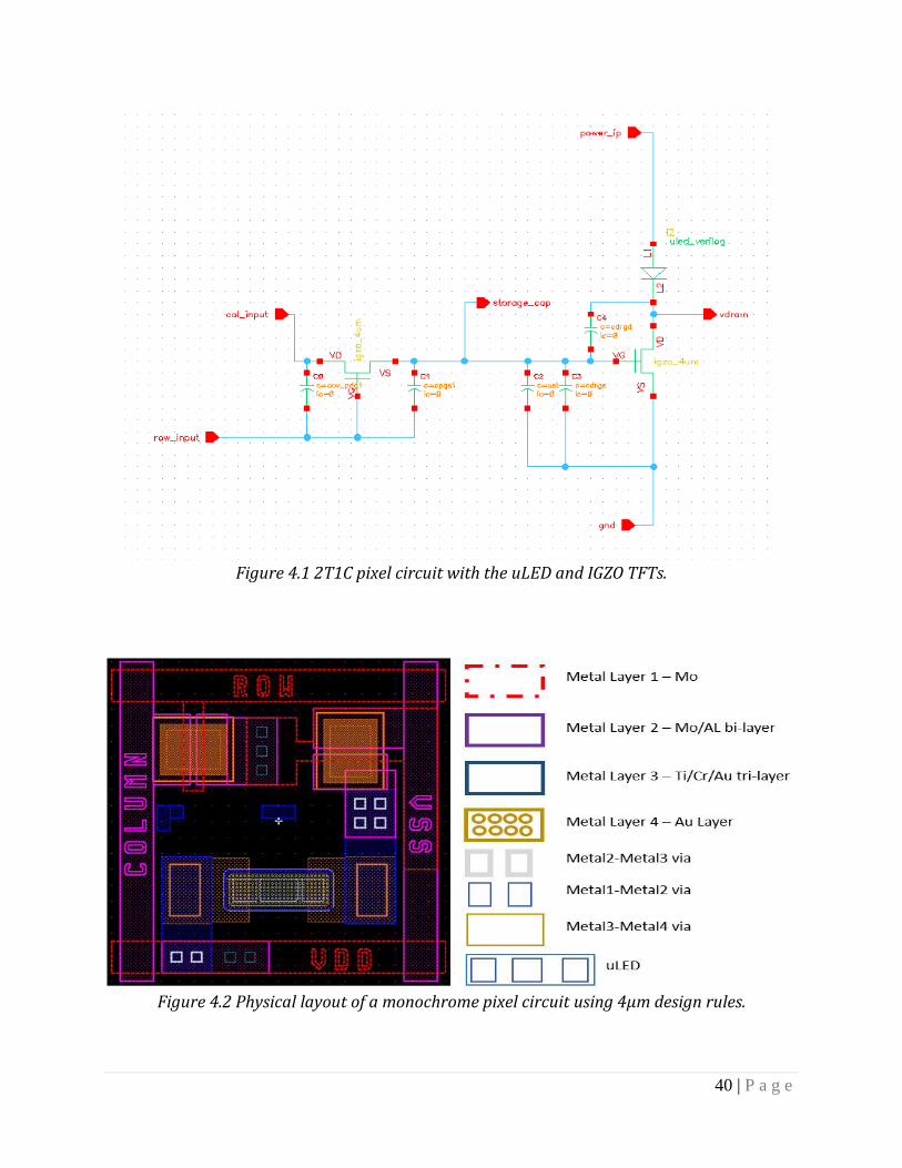
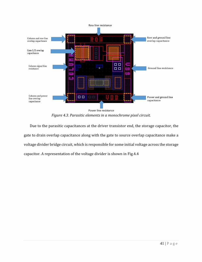
4.1 Pixel Circuit Simulations and impact of parasitic elements
The pixel circuit simulations with the TFT and the uLED model were done to understand
the operation of the pixel circuit and to establish an appropriate value of the storage
capacitor in the design. Cadence Virtuoso environment is used for the simulation of the pixel
circuit shown with parasitic elements in Fig. 4.1. The first transistor is known as the pass
transistor and is connected to the row and the column input, the second transistor is the
driver transistor which is connected to the uLED. Both the transistors have parasitic
capacitances between the gate-drain and gate-source terminals. The parasitic capacitances
are due to the source/drain overlaps with the gate terminal; a physical layout of the design
is shown in Fig. 4.2. The layout is done with 4 µm design rules (i.e. overlaps and spacing),
with the pitch of each pixel being 200 µm. The row and column inputs are applied using the
shift registers and follow the timings as given in Table 1. The voltage across the storage
capacitor controls the driver transistor, which serves as the current source for the uLED.
40 | P a g e
Figure 4.1 2T1C pixel circuit with the uLED and IGZO TFTs.
Figure 4.2 Physical layout of a monochrome pixel circuit using 4µm design rules.
41 | P a g e
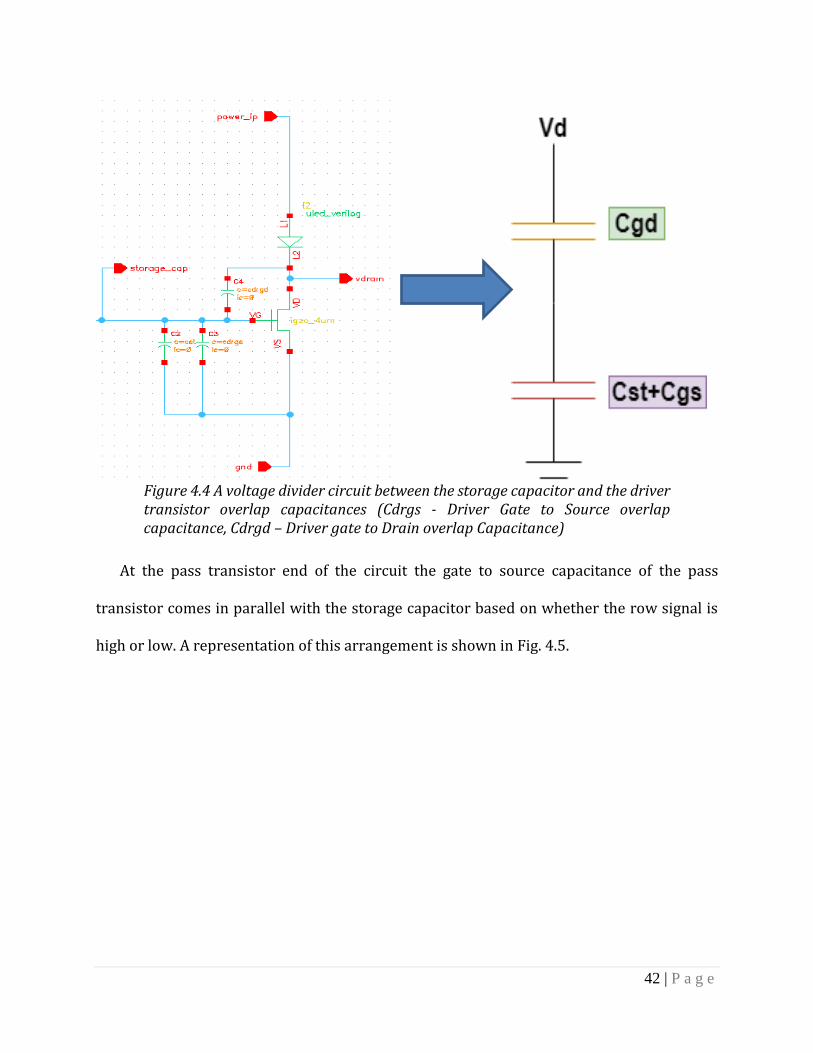
Figure 4.3. Parasitic elements in a monochrome pixel circuit.
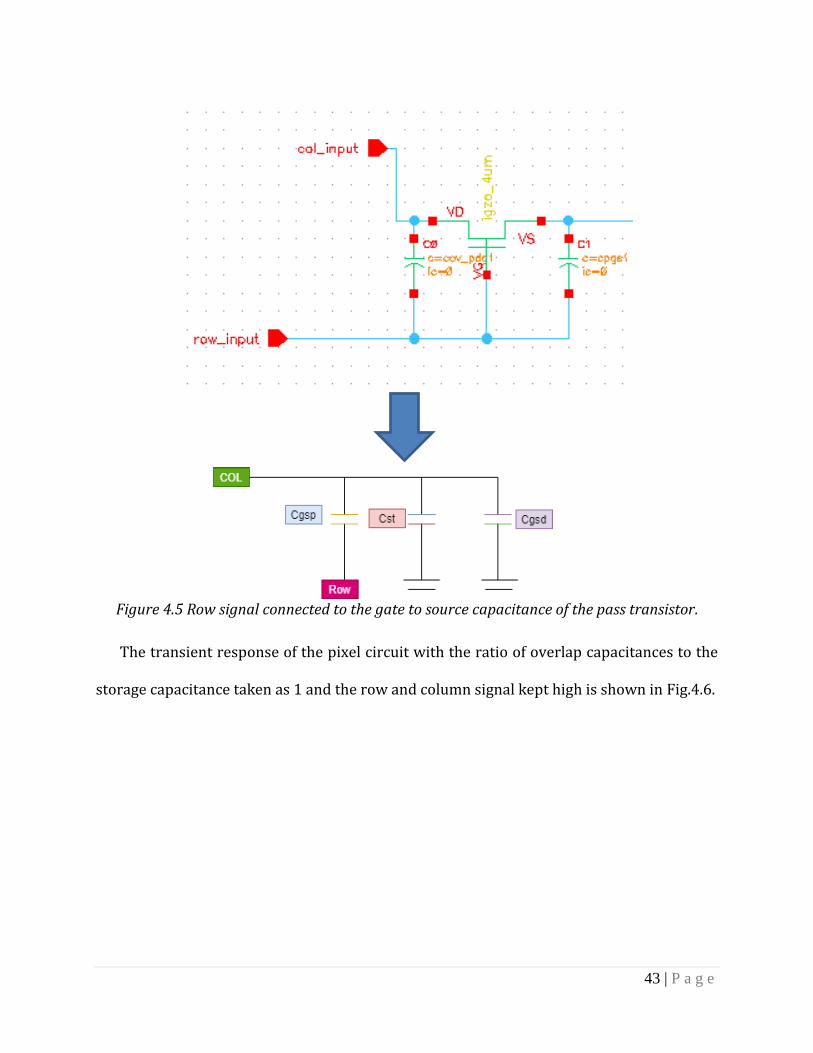
Due to the parasitic capacitances at the driver transistor end, the storage capacitor, the
gate to drain overlap capacitance along with the gate to source overlap capacitance make a
voltage divider bridge circuit, which is responsible for some initial voltage across the storage
capacitor. A representation of the voltage divider is shown in Fig.4.4
42 | P a g e
Figure 4.4 A voltage divider circuit between the storage capacitor and the driver transistor overlap capacitances (Cdrgs - Driver Gate to Source overlap capacitance, Cdrgd – Driver gate to Drain overlap Capacitance)
At the pass transistor end of the circuit the gate to source capacitance of the pass
transistor comes in parallel with the storage capacitor based on whether the row signal is
high or low. A representation of this arrangement is shown in Fig. 4.5.
43 | P a g e
Figure 4.5 Row signal connected to the gate to source capacitance of the pass transistor.
The transient response of the pixel circuit with the ratio of overlap capacitances to the
storage capacitance taken as 1 and the row and column signal kept high is shown in Fig.4.6.
44 | P a g e
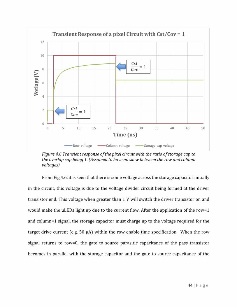
Figure 4.6 Transient response of the pixel circuit with the ratio of storage cap to the overlap cap being 1. (Assumed to have no skew between the row and column voltages)
From Fig.4.6, it is seen that there is some voltage across the storage capacitor initially
in the circuit, this voltage is due to the voltage divider circuit being formed at the driver
transistor end. This voltage when greater than 1 V will switch the driver transistor on and
would make the uLEDs light up due to the current flow. After the application of the row=1
and column=1 signal, the storage capacitor must charge up to the voltage required for the
target drive current (e.g. 50 µA) within the row enable time specification. When the row
signal returns to row=0, the gate to source parasitic capacitance of the pass transistor
becomes in parallel with the storage capacitor and the gate to source capacitance of the
0
2
4
6
8
10
12
0 5 10 15 20 25 30 35 40 45 50
Vo
tla
ge
(V)
Time (us)
Transient Response of a pixel Circuit with Cst/Cov = 1
Row_voltage Column_voltage Storage_cap_voltage
𝐶𝑠𝑡
𝐶𝑜𝑣= 1
𝐶𝑠𝑡
𝐶𝑜𝑣= 1

45 | P a g e
driver transistor. This charge sharing results in a loss of voltage at the storage capacitor; the
drop across the storage capacitor is more when the ratio of 𝐶𝑠𝑡
𝐶𝑜𝑣 is less.
The ratio of storage capacitor to the overlap capacitance is important in order to mitigate
both of these voltage offset issues described. A higher value of storage capacitance was used
in the simulation to get the ratio of 𝐶𝑠𝑡
𝐶𝑜𝑣 = 33, with the results shown in Fig.4.7. The initial
voltage across the storage capacitor is below 1V, and the voltage drop when the row signal
is removed is minimal. Note that for this ratio of 𝐶𝑠𝑡
𝐶𝑜𝑣 , the real estate consumption would be
prohibitive, and would result in a high transient response time (Z) which will cause the
column data latch to be delayed further.
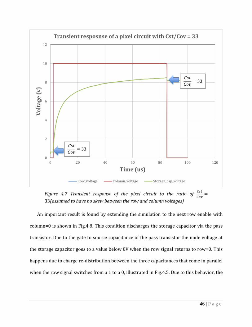
46 | P a g e
Figure 4.7 Transient response of the pixel circuit to the ratio of 𝐶𝑠𝑡
𝐶𝑜𝑣=
33(assumed to have no skew between the row and column voltages)
An important result is found by extending the simulation to the next row enable with
column=0 is shown in Fig.4.8. This condition discharges the storage capacitor via the pass
transistor. Due to the gate to source capacitance of the pass transistor the node voltage at
the storage capacitor goes to a value below 0V when the row signal returns to row=0. This
happens due to charge re-distribution between the three capacitances that come in parallel
when the row signal switches from a 1 to a 0, illustrated in Fig.4.5. Due to this behavior, the
0
2
4
6
8
10
12
0 20 40 60 80 100 120
Vo
lta
ge
(v
)
Time (us)
Transient resposnse of a pixel circuit with Cst/Cov = 33
Row_voltage Column_voltage Storage_cap_voltage
𝐶𝑠𝑡
𝐶𝑜𝑣= 33
𝐶𝑠𝑡
𝐶𝑜𝑣= 33
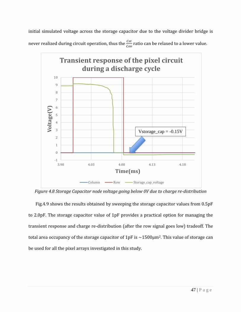
47 | P a g e
initial simulated voltage across the storage capacitor due to the voltage divider bridge is
never realized during circuit operation, thus the 𝐶𝑠𝑡
𝐶𝑜𝑣 ratio can be relaxed to a lower value.
Figure 4.8 Storage Capacitor node voltage going below 0V due to charge re-distribution
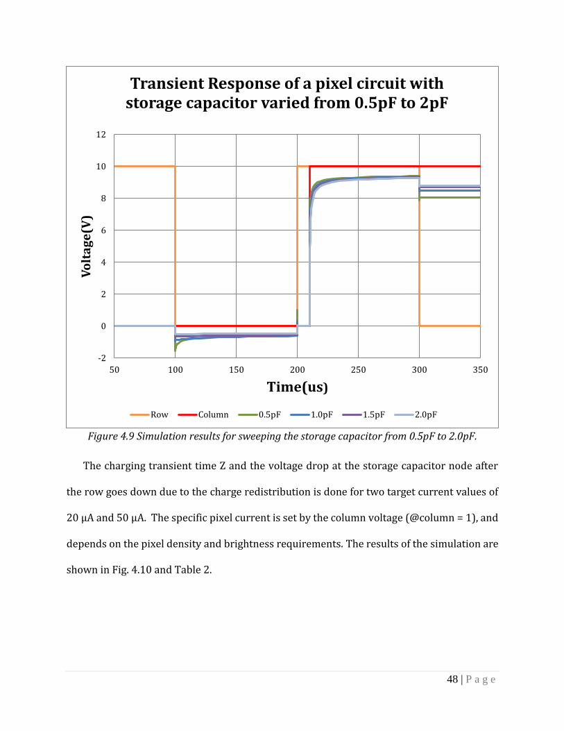
Fig.4.9 shows the results obtained by sweeping the storage capacitor values from 0.5pF
to 2.0pF. The storage capacitor value of 1pF provides a practical option for managing the
transient response and charge re-distribution (after the row signal goes low) tradeoff. The
total area occupancy of the storage capacitor of 1pF is ~1500µm2. This value of storage can
be used for all the pixel arrays investigated in this study.
-1
0
1
2
3
4
5
6
7
8
9
10
3.98 4.03 4.08 4.13 4.18
Vo
lta
ge
(V)
Time(ms)
Transient response of the pixel circuit during a discharge cycle
Column Row Storage_cap_voltage
Vstorage_cap = -0.15V
48 | P a g e
Figure 4.9 Simulation results for sweeping the storage capacitor from 0.5pF to 2.0pF.
The charging transient time Z and the voltage drop at the storage capacitor node after
the row goes down due to the charge redistribution is done for two target current values of
20 µA and 50 µA. The specific pixel current is set by the column voltage (@column = 1), and
depends on the pixel density and brightness requirements. The results of the simulation are
shown in Fig. 4.10 and Table 2.
-2
0
2
4
6
8
10
12
50 100 150 200 250 300 350
Vo
lta
ge
(V)
Time(us)
Transient Response of a pixel circuit with storage capacitor varied from 0.5pF to 2pF
Row Column 0.5pF 1.0pF 1.5pF 2.0pF
49 | P a g e
Figure 4.10 Simulation results for storage capacitor value of 1pF for a target current value of 50 and 20µA
-2
0
2
4
6
8
10
12
0 50 100 150 200 250 300 350 400 450
Vo
lta
ge
(V)
Time(us)
Transient Reposne for Cs=1pF with 10V & 8V column
Row Column_voltage_10V Column_voltage_8V
Storage_cap_value_10V Storage_cap_value_8V
V
V

50 | P a g e
Cs Z
I@50µA ΔV
I@50µA Z
I@20µA
0.5pF 5.2µs 1.25V 0.92µs
1.0pF 8.2µs 0.8V 2µs
1.5pF 11.3µs 0.61V 2µs
2.0pF 14.2µs 0.51V 2.5µs
Table 2. The 95% pixel charging time (Z) and the voltage drop at the storage node due to charge re-distribution (V) for different values of storage capacitor at I=50 µA. The pixel charging time at I=20 µA is also shown for comparison.
4.2 Pixel Circuit Simulations for Row-line and Column-line RC delay
estimations
The physical layout with parasitic elements labelled in a monochrome pixel circuit is
shown in Fig.4.3. The monochrome pixel design is made with four metal layers, the row and
power signals are in the 1st metal layer which is made of 150nm thick molybdenum, the
column and the ground signals are on the 2nd layer which is a bilayer of Molybdenum and
Aluminum and has a total thickness of 150nm (50nm of Mo + 100nm of Al), the uLED is
connected to the 4th layer which is of Gold (0.5µm) and the 3rd layer facilitates the connection
between the metal 2 and metal 4. The material choice for these layers is the main
contributing factor for the resistance offered by the signal lines, while the overlap regions
between the layers is the main contributing factor for the capacitances on the signal lines.
The impact of these parasitic elements on the row and column signal lines is the RC delay
offered by them whose values becomes big as the row or column signal propagate in the pixel
array. Since the thickness of the di-electric between the metal 2 and metal 3 and between
metal 3 and metal 4 is high relative to the thickness of the dielectric between the metal 1 and

51 | P a g e
metal 2 , so only the overlap capacitance between the metal 1 and metal 2 is taken . Sheet
resistances for the 150 nm Molybdenum and 150nm Moly-Al bilayer was obtained to be 1 Ω
per square and 0.37 Ω per square respectively. The width of all the signals in the layout is
20µm and the entire pitch of the pixel is 200µm hence a total of 10 squares are present per
pixel. For the row signal the capacitance is contributed by the gate source/drain overlap
capacitance, the column and row overlap capacitance and the capacitance offered by the
transistor channel. The thickness of the interlayer dielectric (SiO2) between the metal 1 and
metal 2 is 50nm and the constant of relative permittivity is 3.9. For the column signal the
overlap capacitance between the column signal line and the row signal on one end and the
column signal and the power signal on the other end is taken.
Signal name Resistance (Sheet Resistance x No
of squares) Overlap Capacitance
Row 10 Ω/px 0.8pF/px
Column 3.7 Ω/px 0.5pF/px
Power (Vdd) 10 Ω/px 0.5pF/px
Ground (Vss) 3.7 Ω/px 0.5pF/px
Table 3. Resistance and Capacitance values for the row, column, power and ground signals per pixel in a monochrome pixel design.
The values for the row and column resistance and capacitance shown in the Table 3 can
now be used for the circuit simulations to estimate the RC delay. A representation of the RC
network offered by the row signal for a 10x10 arrangement is shown in Fig.4.11, this
schematic is instantiated for the scaled up matrices of 50x50, 380x380. The row signal must
reach the last column within the row enable time for each array arrangement. Fig.4.12 and
Fig.4.13 shows the simulation results for the row-line RC delay and column-line RC delay
values for all the configurations. The row-line RC delay (X) is dependent upon the row line
52 | P a g e
resistance offered due to the relatively higher sheet resistance of the Moly metal layer.
Similarly the column-line RC delay (Y) was found for a line resistance value of 3.7Ω/px and
an overlap capacitance of 0.5pF/px. Table 4 summarizes the results obtained for the X, Y and Z
values for different matrices in this design and gives the Tmin and compares it with the Tmax
calculated for different brightness and refresh rate combinations.
Figure 4.11. A ladder network of resistances and capacitances on a row line for a 10x10 pixel array.
53 | P a g e
Figure 4.12. Results of the row-line RC delay(X) simulations for all the matrices with a row line resistance of 10Ω/px and an overlap capacitance of 0.8pF/px.
0
2
4
6
8
10
12
0 10 20 30 40 50
Vo
lta
ge
(V)
Time(us)
Row RC delay with Rrow=10Ω/px andCov =0.8pF/px
Row 10x10_RC_delay
50x50_RC_delay 380x380_RC_delay
54 | P a g e
Figure 4.13. Results of the column-line RC delay(Y) simulations for all the matrices with a row line resistance of 3.7Ω/px and an overlap capacitance of 0.5pF/px.
0
2
4
6
8
10
12
0 10 20 30 40 50
Vo
lta
ge
(v)
Time (us)
Column RC delay with Rcol=3.7Ω/px and Cov=0.5pF/px
Column 10x10_RC_delay
50x50_RC_delay 380x380_RC_delay
55 | P a g e
Table 4. Timing Specifications for two target current values for 50x50 and 380x380 matrices with the row line resistance and capacitance of 10Ω and an 0.8pF and column line resistance and capacitance of 3.7Ω/px and 0.5pF/px. TmaxA, TmaxB, and TmaxC are maximum row enable times at scan rates of 240 Hz, 480 Hz, and 960 Hz, respectively (see Table 1).
4.3 Pixel Circuit Simulation to estimate IR loss effects
In addition to the timing impact, the parasitic resistance is also responsible for voltage
losses in a uLED backplane system. Since the uLEDs are current operated devices, the
brightness of the ULED is dependent upon the amount of current that flows through it. This
current when accumulated over an entire row of pixels can cause power loss in the power
rail, which can result in uneven brightness one moves down the uLED pixel matrix.
The impact of the IR losses on an individual pixel can be assessed by varying the supply
voltage between a range of voltage values and looking at its impact on the current flowing
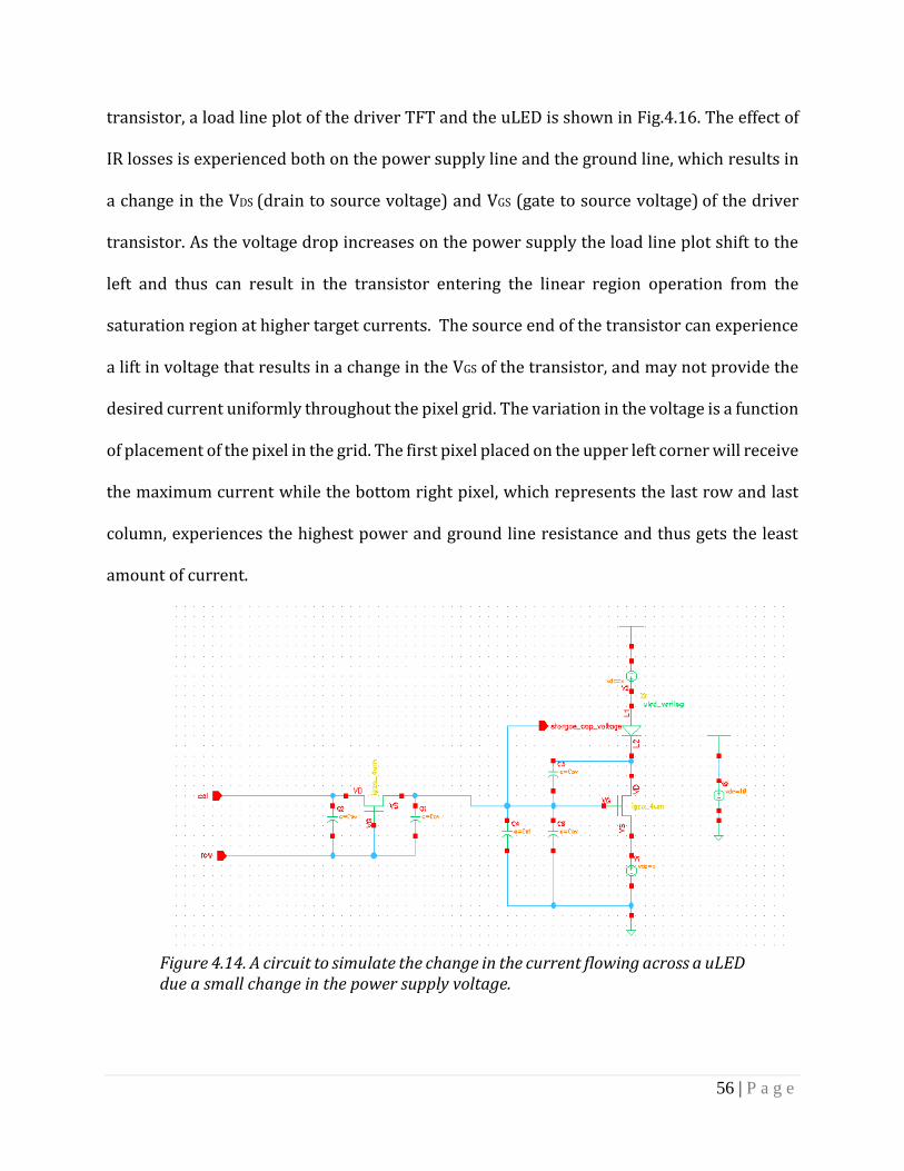
through the uLED. A simulation environment analyze this was setup as shown in Fig.4.14.
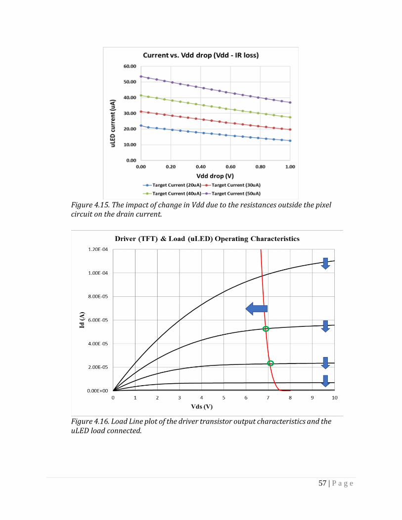
The power supply voltage and ground voltage was varied from 0 to 1V which represented
the change in the potential due to IR losses on the power and ground signal lines. The results
of the simulation are shown in Fig.4.15, which clearly show that as the voltage losses increase
the current flowing through the uLED decreases. This observation can be explained from a
load line characteristic of the driver TFT where the uLED is the load connected on the driver
56 | P a g e
transistor, a load line plot of the driver TFT and the uLED is shown in Fig.4.16. The effect of
IR losses is experienced both on the power supply line and the ground line, which results in
a change in the VDS (drain to source voltage) and VGS (gate to source voltage) of the driver
transistor. As the voltage drop increases on the power supply the load line plot shift to the
left and thus can result in the transistor entering the linear region operation from the
saturation region at higher target currents. The source end of the transistor can experience
a lift in voltage that results in a change in the VGS of the transistor, and may not provide the
desired current uniformly throughout the pixel grid. The variation in the voltage is a function
of placement of the pixel in the grid. The first pixel placed on the upper left corner will receive
the maximum current while the bottom right pixel, which represents the last row and last
column, experiences the highest power and ground line resistance and thus gets the least
amount of current.
Figure 4.14. A circuit to simulate the change in the current flowing across a uLED due a small change in the power supply voltage.
57 | P a g e
Figure 4.15. The impact of change in Vdd due to the resistances outside the pixel circuit on the drain current.
Figure 4.16. Load Line plot of the driver transistor output characteristics and the uLED load connected.
58 | P a g e
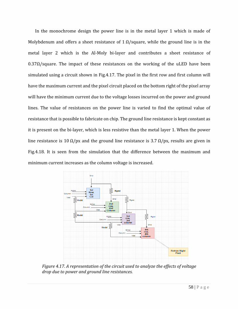
In the monochrome design the power line is in the metal layer 1 which is made of
Molybdenum and offers a sheet resistance of 1 Ω/square, while the ground line is in the
metal layer 2 which is the Al-Moly bi-layer and contributes a sheet resistance of
0.37Ω/square. The impact of these resistances on the working of the uLED have been
simulated using a circuit shown in Fig.4.17. The pixel in the first row and first column will
have the maximum current and the pixel circuit placed on the bottom right of the pixel array
will have the minimum current due to the voltage losses incurred on the power and ground
lines. The value of resistances on the power line is varied to find the optimal value of
resistance that is possible to fabricate on chip. The ground line resistance is kept constant as
it is present on the bi-layer, which is less resistive than the metal layer 1. When the power
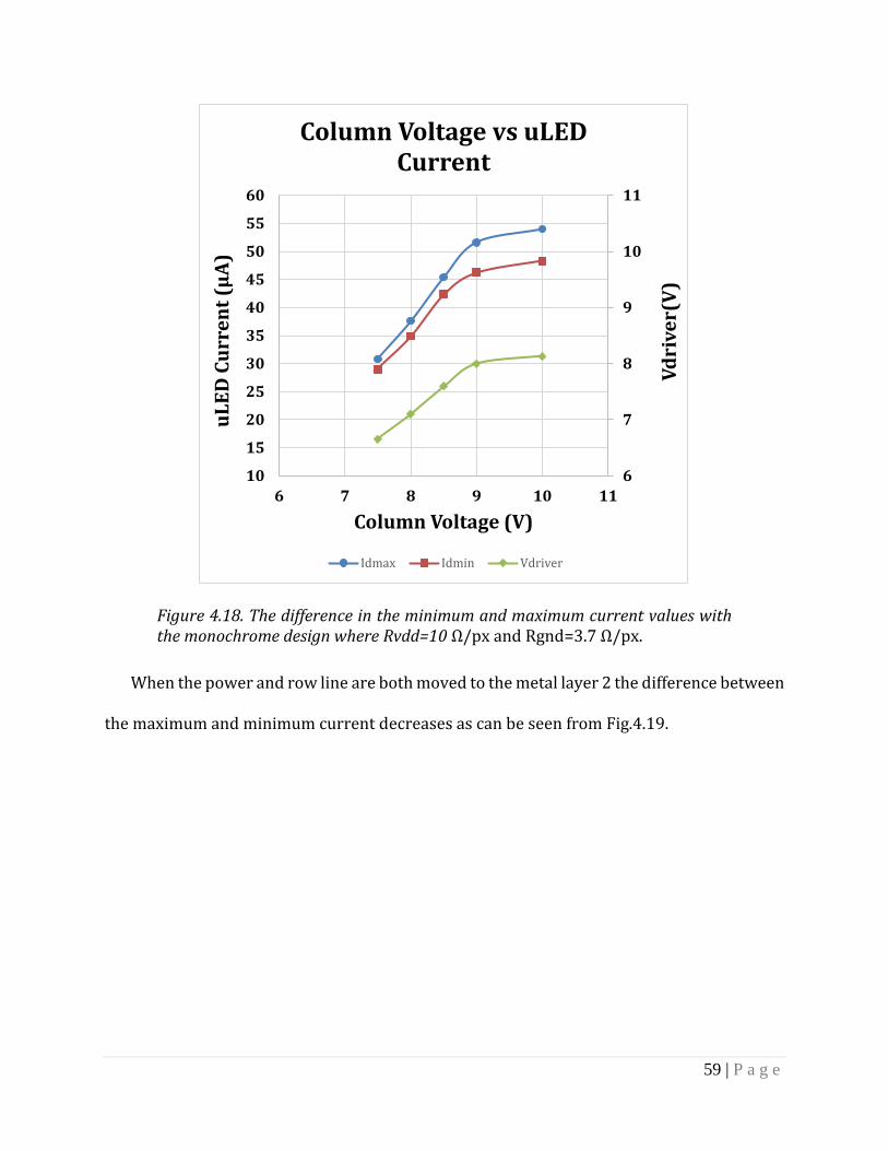
line resistance is 10 Ω/px and the ground line resistance is 3.7 Ω/px, results are given in
Fig.4.18. It is seen from the simulation that the difference between the maximum and
minimum current increases as the column voltage is increased.
Figure 4.17. A representation of the circuit used to analyze the effects of voltage drop due to power and ground line resistances.
59 | P a g e
Figure 4.18. The difference in the minimum and maximum current values with the monochrome design where Rvdd=10 Ω/px and Rgnd=3.7 Ω/px.
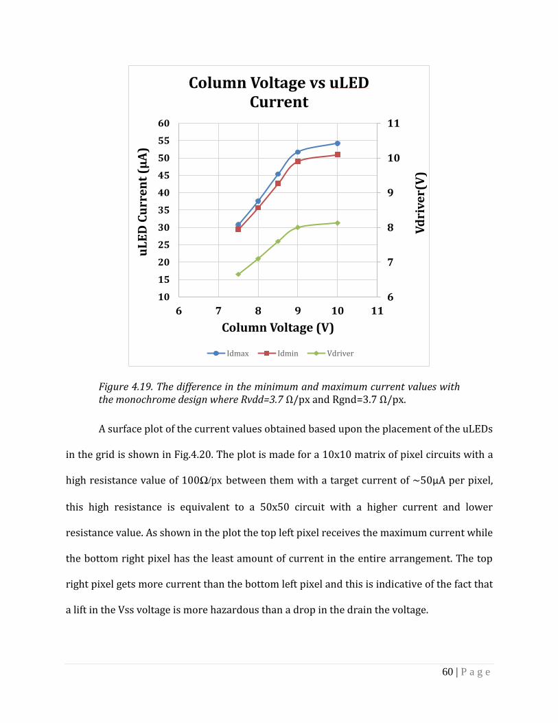
When the power and row line are both moved to the metal layer 2 the difference between
the maximum and minimum current decreases as can be seen from Fig.4.19.
6
7
8
9
10
11
10
15
20
25
30
35
40
45
50
55
60
6 7 8 9 10 11
Vd
riv
er(
V)
uL
ED
Cu
rre
nt
(µA
)
Column Voltage (V)
Column Voltage vs uLED Current
Idmax Idmin Vdriver
60 | P a g e
Figure 4.19. The difference in the minimum and maximum current values with the monochrome design where Rvdd=3.7 Ω/px and Rgnd=3.7 Ω/px.
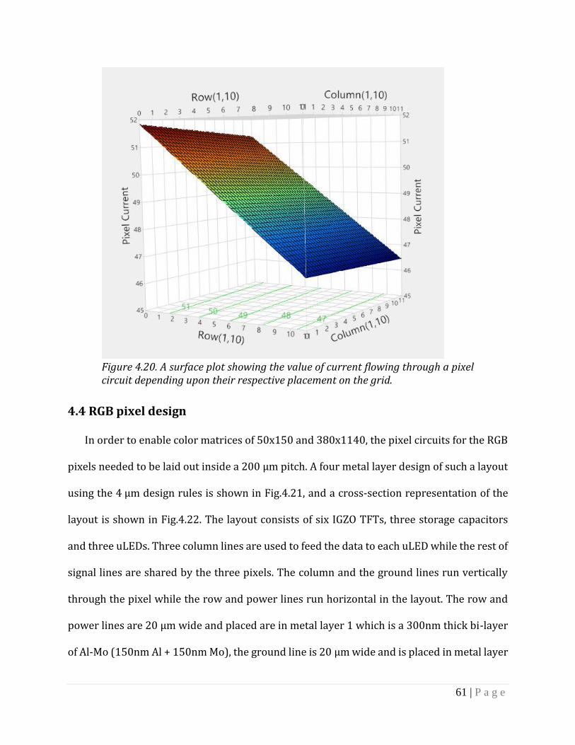
A surface plot of the current values obtained based upon the placement of the uLEDs
in the grid is shown in Fig.4.20. The plot is made for a 10x10 matrix of pixel circuits with a
high resistance value of 100Ω/px between them with a target current of ~50µA per pixel,
this high resistance is equivalent to a 50x50 circuit with a higher current and lower
resistance value. As shown in the plot the top left pixel receives the maximum current while
the bottom right pixel has the least amount of current in the entire arrangement. The top
right pixel gets more current than the bottom left pixel and this is indicative of the fact that
a lift in the Vss voltage is more hazardous than a drop in the drain the voltage.
6
7
8
9
10
11
10
15
20
25
30
35
40
45
50
55
60
6 7 8 9 10 11
Vd
riv
er(
V)
uL
ED
Cu
rre
nt
(µA
)
Column Voltage (V)
Column Voltage vs uLEDCurrent
Idmax Idmin Vdriver
61 | P a g e
Figure 4.20. A surface plot showing the value of current flowing through a pixel circuit depending upon their respective placement on the grid.
4.4 RGB pixel design
In order to enable color matrices of 50x150 and 380x1140, the pixel circuits for the RGB
pixels needed to be laid out inside a 200 µm pitch. A four metal layer design of such a layout
using the 4 µm design rules is shown in Fig.4.21, and a cross-section representation of the
layout is shown in Fig.4.22. The layout consists of six IGZO TFTs, three storage capacitors
and three uLEDs. Three column lines are used to feed the data to each uLED while the rest of
signal lines are shared by the three pixels. The column and the ground lines run vertically
through the pixel while the row and power lines run horizontal in the layout. The row and
power lines are 20 µm wide and placed are in metal layer 1 which is a 300nm thick bi-layer
of Al-Mo (150nm Al + 150nm Mo), the ground line is 20 µm wide and is placed in metal layer
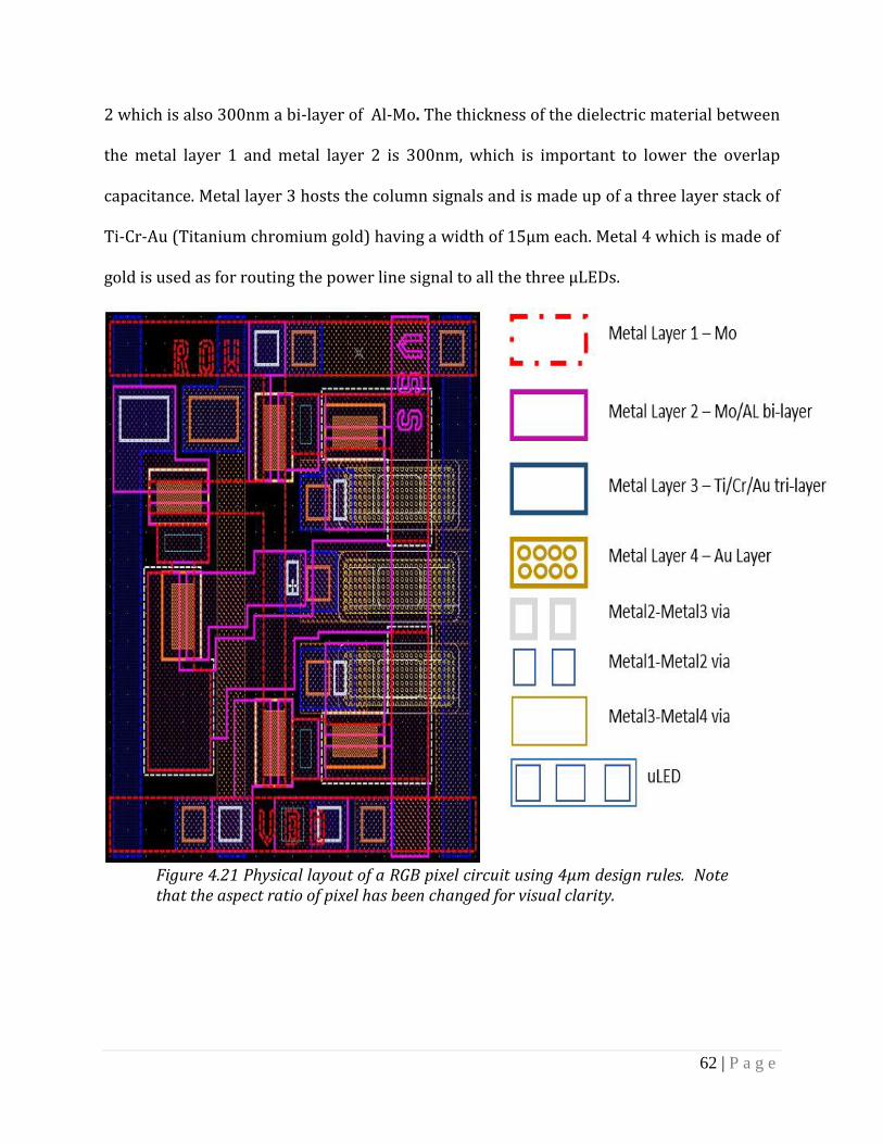
62 | P a g e
2 which is also 300nm a bi-layer of Al-Mo. The thickness of the dielectric material between
the metal layer 1 and metal layer 2 is 300nm, which is important to lower the overlap
capacitance. Metal layer 3 hosts the column signals and is made up of a three layer stack of
Ti-Cr-Au (Titanium chromium gold) having a width of 15µm each. Metal 4 which is made of
gold is used as for routing the power line signal to all the three µLEDs.
Figure 4.21 Physical layout of a RGB pixel circuit using 4µm design rules. Note that the aspect ratio of pixel has been changed for visual clarity.
63 | P a g e
Figure 4.22 A cross-section representation of a driver TFT in a RGB pixel physical layout.
A storage capacitor of 1pF for each pixel circuit is made by overlapping the source of the
driver transistor with the ground line. The parasitic resistance and capacitance on the signal
lines are shown in Fig.4.23 and their values are provided in Table 5.
Figure 4.23 Parasitic elements in a RGB pixel circuit.

64 | P a g e
Signal name Line Resistance Input Capacitance
Row 2.2 Ω/px 1.08pF/px
Column 2.6 Ω/px 0.13pF/px
Power (Vdd) 2.2 Ω/px 0.09pF/px
Ground (Vss) 2.2 Ω/px 0.09pF/px
Table 5. Resistance and Capacitance values for the row, column, power and ground signals per pixel in a RGB pixel design.
The Al-Mo 300nm that makes up the second metal layer has a sheet resistance of
0.22Ω/sq. Each of these signal lines are of 20µm width and thus cover 10 squares in a 200µm
pitch and thus the total resistance of these lines is 2.2Ω/px. The column signal lines are of
15µm each and the sheet resistance of the metal layer 3 is 0.20 Ω/sq, hence the total
resistance of one column line is 2.6 Ω/px over the entire 200 µm length of the layout. The
overlap capacitance on the row line is mainly due to the source/drain overlap capacitance
for each of the three pass gate transistor and the overlap of the row line with the metal layer
2. The thickness of the di-electric layer between the metal layer1 and metal layer2 is 300nm,
thus the total overlap capacitance on the row line is 3x Gate S/D overlap capacitance due to
the three pass gate transistors and the regions of overlap resulting in 1.08 pF/px. There are
three column carrying data in a RGB pixel design, the slowest column will be taken for the
calculation of Y, since all the columns are of the same width and are present on the same
metal layer thus have the same line resistance. The differentiating factor between the three
columns is in the overlap capacitance values which determines the slowest column. From
the layout it was determined that the middle column had the maximum area of overlap
(1140µm2) amongst all the three columns. The power and ground lines have an overlap
capacitance of 0.09pF/px each. The resistance on all the signal lines is 2.2 Ω/px as they are
65 | P a g e
all made with the bi-layer material, Table 6 gives the timing specification with these new
values and compares it with Tmax values at different scan rates.
Table 6. Timing Specifications for two target current values for 50x50 and 380x380 matrices with the row line resistance and capacitance of 10Ω/px and an 0.8pF/px and column line resistance and capacitance of 3.7Ω/px and 0.5pF/px. TmaxA, TmaxB, and TmaxC are maximum row enable times at scan rates of 240 Hz, 480 Hz, and 960 Hz, respectively.
4.5 Summary
This chapter covered the impact of parasitic resistance and capacitance on the
performance of a pixel matrix. The effects of these parasitic elements were analyzed for the
monochrome pixel design and the conclusions from the analysis served as the considerations
for the RGB pixel design. A comparison between the X,Y and Z values with the Tmax for a
monochrome pixel circuit was shown. The use of Al-Mo bilayer material for the row and
power line signal and the increase in the di-electric thickness to 300nm between the metal
layer 1 and metal layer 2 was proven to be beneficial in reducing the timing delay and IR
losses. A new RGB pixel design was made using the 4µm design rules. Finally, a comparison
between the new timing values of X, Y, Z obtained with the new pixel design was done with
the Tmax . The next chapter will cover the bonding techniques that can be used to bond the
glass substrate with the PCB.
66 | P a g e
V. Electrical bonding between glass and PCB
5.1 Bonding Techniques
The pixel array on glass and the controller circuit on the PCB need to be electrically
connected for the complete backplane design. Bonding between the PCB and glass falls in the
realms of electronics packaging, there are various ways of making electrical connection
between two substrates ranging from wire bonding to anisotropic conductive film bonding
(ACF). This section will give an introduction to the two commonly used bonding techniques,
the flip chip bonding and adhesive film bonding.
5.1.1 Flip Chip Bonding
Flip chip bonding is a technique of connecting the chip ‘face down’ onto a
substrate. Metal bumps are formed on the pads present on the top of the wafer which
are reflowed and then the chip is flipped and placed on top of a substrate that has
matching pads. This assembly is then under filled with an epoxy resin, a representation
of a flip chip bonding process is shown in Fig.5.1. This technology has the advantage of
shorter leads, offers lower inductance and provides higher density for making
connections, lead and tin based solders are the most commonly used solder bump
materials. This method of bonding with tin based solder materials has limitations when
used for temperature sensitive applications like the LCD bonding or for applications
involving organic transistors as the reflow temperatures for these solder materials is
high. The use of curing adhesives for making interconnection is a popular alternative to
the flip chip boding technique as a low temperature process.
67 | P a g e
Figure 5.1 A conventional Flip Chip bonding process [12].
5.1.2 Anisotropic Conductive Film Bonding (ACF)
The use of curing adhesives provide for a low temperature bonding process. The
bonding takes place by making a mechanical contact between the bumps present on the
chip and the corresponding bumps on the substrate after curing the adhesive. These
adhesives are of two types: Anisotropic Conductive Film (ACF) and Non-conductive
adhesive (NCA). ACF has conductive particles in its adhesive film while the NCA does
not have conductive particles in the adhesive film. In ACF bonding the conductive film
is cut out in the shape of the chip and applied on it, a mechanical compressive force is
applied in the vertical direction between the chip and the substrate which forces the
conductive particles in the ACF to align themselves between the chip and the substrate
pads in the z direction. Heat energy is then applied for the conductive film to cure and
maintain a mechanical connection. A conventional ACF process is shown in Fig.5.2. The
IGZO-TFTs used for this design are sensitive to a thermal stress greater than 200OC [7].
The sensitivity to the thermal stress was shown to go down at lower channel length
devices as can be seen from Fig.5.3, hence 200OC is considered as the safe limit of
operation for the 4µm channel length devices used in this project. As can be seen from
Fig.5.4, even at a temperature of 170oC ACF bonding can withstand a load greater than
25N for both chip on glass (COG) and chip on flex (COF) techniques.
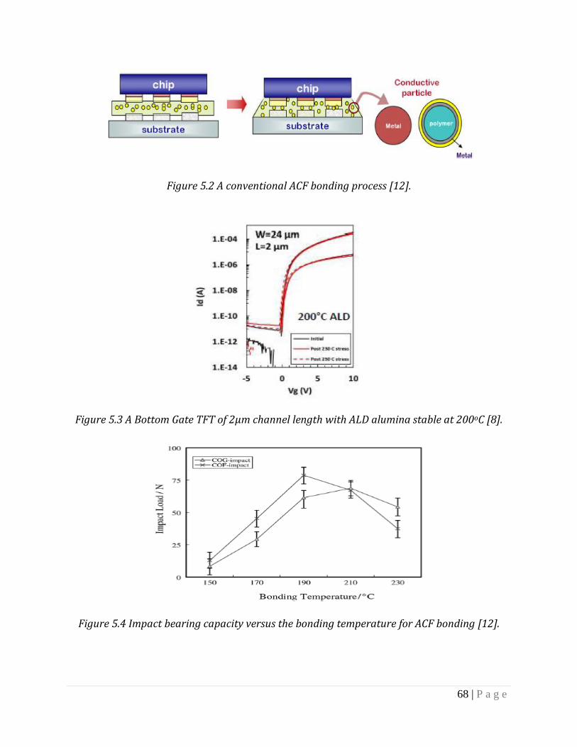
68 | P a g e
Figure 5.2 A conventional ACF bonding process [12].
Figure 5.3 A Bottom Gate TFT of 2µm channel length with ALD alumina stable at 200oC [8].
Figure 5.4 Impact bearing capacity versus the bonding temperature for ACF bonding [12].
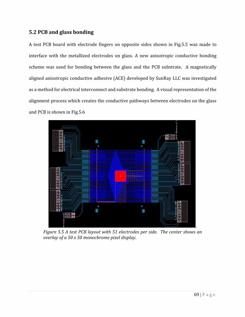
69 | P a g e
5.2 PCB and glass bonding
A test PCB board with electrode fingers on opposite sides shown in Fig.5.5 was made to
interface with the metallized electrodes on glass. A new anisotropic conductive bonding
scheme was used for bonding between the glass and the PCB substrate. A magnetically
aligned anisotropic conductive adhesive (ACE) developed by SunRay LLC was investigated
as a method for electrical interconnect and substrate bonding. A visual representation of the
alignment process which creates the conductive pathways between electrodes on the glass
and PCB is shown in Fig.5.6
. Figure 5.5 A test PCB layout with 51 electrodes per side. The center shows an overlay of a 50 x 50 monochrome pixel display.
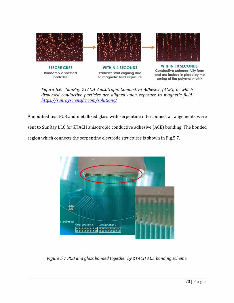
70 | P a g e
Figure 5.6. SunRay ZTACH Anisotropic Conductive Adhesive (ACE), in which dispersed conductive particles are aligned upon exposure to magnetic field. https://sunrayscientific.com/solutions/
A modified test PCB and metallized glass with serpentine interconnect arrangements were
sent to SunRay LLC for ZTACH anisotropic conductive adhesive (ACE) bonding. The bonded
region which connects the serpentine electrode structures is shown in Fig.5.7.
Figure 5.7 PCB and glass bonded together by ZTACH ACE bonding scheme.
71 | P a g e
Each finger electrode has a metal contact pad of 450µm diameter that contributes to ~0.3Ω
of resistance. The graph of resistance vs. number of contacts is shown in Fig.5.8
Figure 5.8 Resistance vs number of vias on the test PCB.
The contact resistance was calculated (i.e. resistance × area) to be 0.05Ω-mm2. This
experiment verified that the ZTACH ACE bonding technique can be used for this interconnect
bonding process, and will serve as the preferred technique for all pixel matrix displays.
5.3 Wrap-around Electrodes
The uLED backplane technology is aimed to make large displays through a modular
approach. Small size uLED backplane can be placed right next to each other in a tiled fashion
to make up a big display. A representation of such an arrangement is shown in Fig. 5.9, each
module in this arrangement receives the signals from a PCB electrically bonded to it on the
back of the glass and then those signals are routed using electrodes to the front of the glass
which has the TFT backplane. These electrodes are known as wrap-around electrodes; the
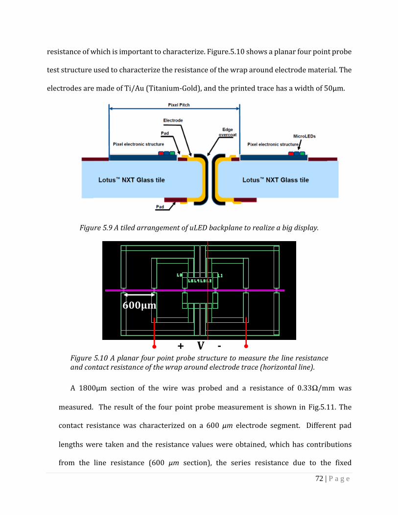
72 | P a g e
resistance of which is important to characterize. Figure.5.10 shows a planar four point probe
test structure used to characterize the resistance of the wrap around electrode material. The
electrodes are made of Ti/Au (Titanium-Gold), and the printed trace has a width of 50µm.
Figure 5.9 A tiled arrangement of uLED backplane to realize a big display.
Figure 5.10 A planar four point probe structure to measure the line resistance and contact resistance of the wrap around electrode trace (horizontal line).
A 1800µm section of the wire was probed and a resistance of 0.33Ω/mm was
measured. The result of the four point probe measurement is shown in Fig.5.11. The
contact resistance was characterized on a 600 µm electrode segment. Different pad
lengths were taken and the resistance values were obtained, which has contributions
from the line resistance (600 µm section), the series resistance due to the fixed
600µm
+ V -
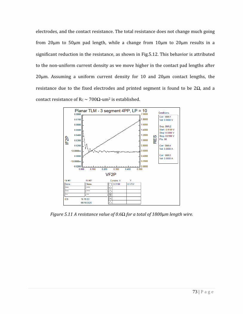
73 | P a g e
electrodes, and the contact resistance. The total resistance does not change much going
from 20µm to 50µm pad length, while a change from 10µm to 20µm results in a
significant reduction in the resistance, as shown in Fig.5.12. This behavior is attributed
to the non-uniform current density as we move higher in the contact pad lengths after
20µm. Assuming a uniform current density for 10 and 20µm contact lengths, the
resistance due to the fixed electrodes and printed segment is found to be 2Ω, and a
contact resistance of RC ~ 700Ω-um2 is established.
Figure 5.11 A resistance value of 0.6Ω for a total of 1800µm length wire.
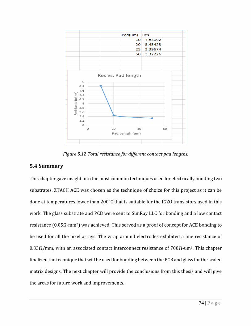
74 | P a g e
Figure 5.12 Total resistance for different contact pad lengths.
5.4 Summary
This chapter gave insight into the most common techniques used for electrically bonding two
substrates. ZTACH ACE was chosen as the technique of choice for this project as it can be
done at temperatures lower than 200oC that is suitable for the IGZO transistors used in this
work. The glass substrate and PCB were sent to SunRay LLC for bonding and a low contact
resistance (0.05Ω-mm2) was achieved. This served as a proof of concept for ACE bonding to
be used for all the pixel arrays. The wrap around electrodes exhibited a line resistance of
0.33Ω/mm, with an associated contact interconnect resistance of 700Ω-um2. This chapter
finalized the technique that will be used for bonding between the PCB and glass for the scaled
matrix designs. The next chapter will provide the conclusions from this thesis and will give
the areas for future work and improvements.
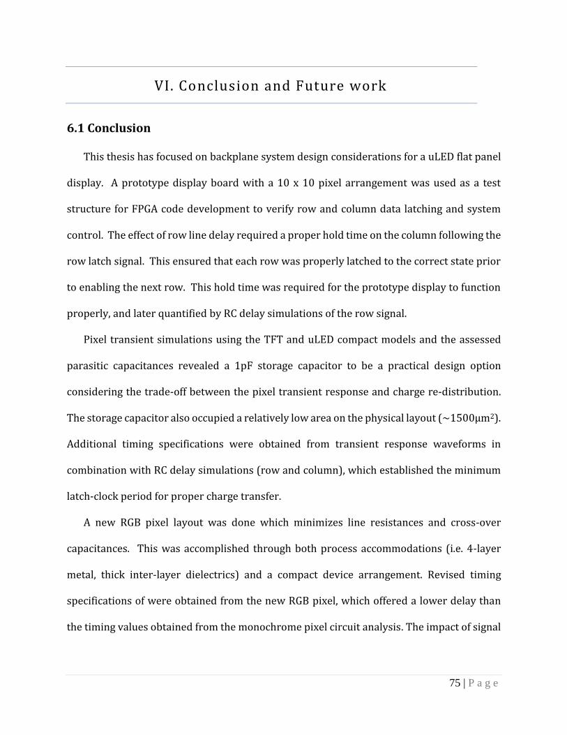
75 | P a g e
VI. Conclusion and Future work
6.1 Conclusion
This thesis has focused on backplane system design considerations for a uLED flat panel
display. A prototype display board with a 10 x 10 pixel arrangement was used as a test
structure for FPGA code development to verify row and column data latching and system
control. The effect of row line delay required a proper hold time on the column following the
row latch signal. This ensured that each row was properly latched to the correct state prior
to enabling the next row. This hold time was required for the prototype display to function
properly, and later quantified by RC delay simulations of the row signal.
Pixel transient simulations using the TFT and uLED compact models and the assessed
parasitic capacitances revealed a 1pF storage capacitor to be a practical design option
considering the trade-off between the pixel transient response and charge re-distribution.
The storage capacitor also occupied a relatively low area on the physical layout (~1500µm2).
Additional timing specifications were obtained from transient response waveforms in
combination with RC delay simulations (row and column), which established the minimum
latch-clock period for proper charge transfer.
A new RGB pixel layout was done which minimizes line resistances and cross-over
capacitances. This was accomplished through both process accommodations (i.e. 4-layer
metal, thick inter-layer dielectrics) and a compact device arrangement. Revised timing
specifications of were obtained from the new RGB pixel, which offered a lower delay than
the timing values obtained from the monochrome pixel circuit analysis. The impact of signal
76 | P a g e
line resistance IR losses was analyzed and an assessment of the associated variation in the
uLED current over a representative array was performed.
A novel magnetically aligned anisotropic conductive adhesive was investigated and
verified to be an ideal option for the electrode interconnection between the PCB and glass
substrate. SunRay ZTACH (ACE) demonstrated ohmic contact behavior and a low contact
resistance of 0.05Ω-mm2, translating to an added electrode resistance of less than 3 Ω. The
wrap around electrodes traces were also shown to have very low contact resistance of
700Ω-um2 and a line resistance of 0.33Ω/mm, translating to an added electrode resistance
of much less than 1 Ω. These resistance values ensure a negligible influence on both RC delay
and IR loss assessments.
6.2 Future Work
This thesis has focused on the design and simulation aspects of a uLED system; system
design validation on TFT pixel arrays remains to be done. The FPGA code written for the
model board needs to be demonstrated on the actual 10x10 pixel arrays, since the transistors
used in the model board are power transistors and not IGZO based transistors as used for
this project; code modifications may be required. System verification must then be extended
to the 50 x 50 pixel array and ultimately the 380 x 380 RGB pixel array.
Operation of the pixel circuit and the impact of line parasitic elements on the
performance of the actual TFT array need to be quantified and compared to simulated values.
The final layout for the 380 x 380 pixel array which adheres to edge space requirements to
ensure seamless tiling must still be designed. Finally, the ZTACH ACE interconnect must be
verified to facilitate actual PCB-display signal control.
77 | P a g e
REFERENCES
[1] Shuichi Uchikoga,Future Trend of Flat Panel Displays and Comparison of its
Driving Methods, Proceedings of the 18th International Symposium on Power
Semiconductor Devices & IC's , June 4-8, 2006 Naples, Italy
[2] Mary Tamar Tan ,Rodger Ricgy, LCD Fundamentals and the LCD Driver Module
of 8-bit PIC Microcontroller, Microchip Technology inc.
[3] Shahin Jafarabadiashtiani , Pixel Circuits and Driving Schemes for Active-Matrix
Organic Light-Emitting Diode Displays , Thesis, University of Waterloo ,Waterloo,
Ontario, Canada, 2007.
[4] H. Hosono, “Ionic amorphous oxide semiconductors: Material design, carrier
transport, and device application,” Journal of Non-Crystalline Solids, vol. 352,no. 9,
pp. 851–858, Jun. 2006.
[5] Prashant Ganesh,Investigation of Thermal Stress Degradation in Indium-
GalliumZinc-Oxide TFTs, Theses,RIT Scholar Works, December 23, 2017.
[6] Hong Jae Shin , Soo Hong Choi ,Jai ye Choi, "A high image quality organic light
emititng diode display with motion blur for ultra high resolution and premium TVs",
Journal of the society for information display,21 June 2020, Wiley online library.
[7] Arokia Nathan, G. Reza Chaji,Driving Schemes for a-Si and LTPS AMOLED
Displays,JOURNAL OF DISPLAY TECHNOLOGY, VOL. 1, NO. 2, DECEMBER 2005
78 | P a g e
[8] M. S. Kabir, R. R. Chowdhury, R. G. Manley, and K. D. Hirschman, "Device Structure
and Passivation Options for the Integration of Scaled IGZO TFTs" , ECS Transactions,
92 (4) 143-151 (2019)
[9] K. D. Hirschman, T. Mudgal, E. Powell and R. G. Manley, "A 2D empirical model for
on-state operation of scaled IGZO TFTs exemplifying the physical response of TCAD
simulation," ECS Transactions, vol. 86, no. 11, pp. 153-166, 2018.
[10] Hector Alejandro Rubio Rivera,"A Semi-Empirical Compact Model for IGZO TFT
to Assess the Impact of Parasitic Elements in Active Matrix Pixel Designs", Theses,
RIT Scholar Works,August 2020
[11] D.J.R. Cristaldi et al., Chapter 6, Drivers for Active-Matrix LCDs ,Liquid Crystal
Display Drivers , Springer Science+Business Media B.V. 2009.
[12] Sun-Chul Kim,Young-Ho Kim,Review paper: Flip chip bonding with anisotropic
conductive film (ACF) and nonconductive adhesive (NCA), Current Applied
Physics,Volume 13, Supplement 2, 20 July 2013, Pages S14-S25
[13] Prashant Ganesh,Investigation of Thermal Stress Degradation in Indium-
GalliumZinc-Oxide TFTs, Theses, RIT Scholar Works, December 23, 2017
[14] Simon Monk,The 74HC595 Shift Register, Arduino Lesson 4. Eight LEDs and a Shift
Register, Adafruit
79 | P a g e
[15] Datasheet CD74HC595N ,Texas Instruments.
[16] Nexys A7 reference manual ,Digilent 2020
[17] G. W. Lee, H. Kim, J. Park, J. Shim and D. Shin, "Investigation of Luminance
Degradation in Organic Light-Emitting Diodes by Impedance Spectroscopy," IEEE
Photonics Technology Letters, vol. 30, no. 13, pp. 1183-1185, 2018.
[18] A. Suresh and J. F. Muth ,Bias stress stability of indium gallium zinc oxide channel
based transparent thin film transistors, Appl. Phys. Lett. 92, 033502 (2008).
[19] Fangwang Gou ,En-Lin ,Guanjun Tan , Yi-Fen Lan, Cheng-Yeh Tsai, Shin-Tson Wu,
High Performance color-converted micro-LED displays, Journal of the society for
information display, 27, March 2019.
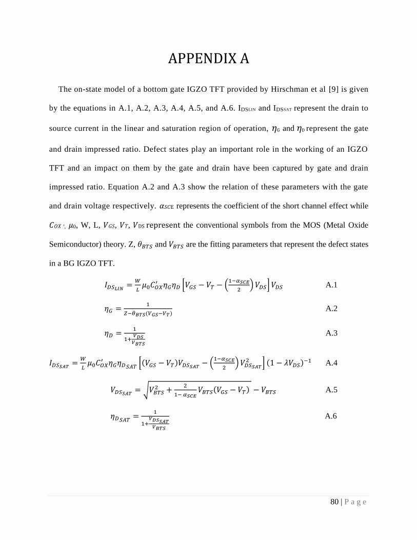
80 | P a g e
APPENDIX A
The on-state model of a bottom gate IGZO TFT provided by Hirschman et al [9] is given
by the equations in A.1, A.2, A.3, A.4, A.5, and A.6. IDSLIN and IDSSAT represent the drain to
source current in the linear and saturation region of operation, 𝜂G and 𝜂D represent the gate
and drain impressed ratio. Defect states play an important role in the working of an IGZO
TFT and an impact on them by the gate and drain have been captured by gate and drain
impressed ratio. Equation A.2 and A.3 show the relation of these parameters with the gate
and drain voltage respectively. 𝛼𝑆𝐶E represents the coefficient of the short channel effect while
𝐶𝑂𝑋 ′, 𝜇0, W, L, 𝑉𝐺𝑆, 𝑉𝑇, 𝑉DS represent the conventional symbols from the MOS (Metal Oxide
Semiconductor) theory. Z, 𝜃𝐵𝑇𝑆 and 𝑉𝐵𝑇𝑆 are the fitting parameters that represent the defect states
in a BG IGZO TFT.
𝐼𝐷𝑆𝐿𝐼𝑁=
𝑊
𝐿𝜇0𝐶𝑂𝑋
′ 𝜂𝐺𝜂𝐷 [𝑉𝐺𝑆 − 𝑉𝑇 − (1−𝛼𝑆𝐶𝐸
2) 𝑉𝐷𝑆] 𝑉𝐷𝑆 A.1
𝜂𝐺 =1
𝑍−𝜃𝐵𝑇𝑆(𝑉𝐺𝑆−𝑉𝑇) A.2
𝜂𝐷 =1
1+𝑉𝐷𝑆
𝑉𝐵𝑇𝑆
A.3
𝐼𝐷𝑆𝑆𝐴𝑇=
𝑊
𝐿𝜇0𝐶𝑂𝑋
′ 𝜂𝐺𝜂𝐷𝑆𝐴𝑇[(𝑉𝐺𝑆 − 𝑉𝑇)𝑉𝐷𝑆𝑆𝐴𝑇
− (1−𝛼𝑆𝐶𝐸
2) 𝑉𝐷𝑆𝑆𝐴𝑇
2 ] (1 − 𝜆𝑉𝐷𝑆)−1 A.4
𝑉𝐷𝑆𝑆𝐴𝑇= √𝑉𝐵𝑇𝑆
2 +2
1− 𝛼𝑆𝐶𝐸𝑉𝐵𝑇𝑆(𝑉𝐺𝑆 − 𝑉𝑇) − 𝑉𝐵𝑇𝑆 A.5
𝜂𝐷𝑆𝐴𝑇=
1
1+𝑉𝐷𝑆𝑆𝐴𝑇
𝑉𝐵𝑇𝑆
A.6
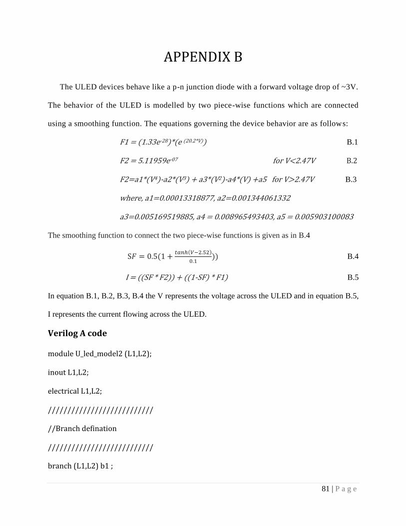
81 | P a g e
APPENDIX B
The ULED devices behave like a p-n junction diode with a forward voltage drop of ~3V.
The behavior of the ULED is modelled by two piece-wise functions which are connected
using a smoothing function. The equations governing the device behavior are as follows:
F1 = (1.33e-28)*(e (20.2*V)) B.1
F2 = 5.11959e-07 for V<2.47V B.2
F2=a1*(V4)-a2*(V3) + a3*(V2)-a4*(V) +a5 for V>2.47V B.3
where, a1=0.00013318877, a2=0.001344061332
a3=0.005169519885, a4 = 0.008965493403, a5 = 0.005903100083
The smoothing function to connect the two piece-wise functions is given as in B.4
S𝐹 = 0.5(1 +𝑡𝑎𝑛ℎ(𝑉−2.52)
0.1)) B.4
I = ((SF * F2)) + ((1-SF) * F1) B.5
In equation B.1, B.2, B.3, B.4 the V represents the voltage across the ULED and in equation B.5,
I represents the current flowing across the ULED.
Verilog A code
module U_led_model2 (L1,L2);
inout L1,L2;
electrical L1,L2;
///////////////////////////
//Branch defination
///////////////////////////
branch (L1,L2) b1 ;
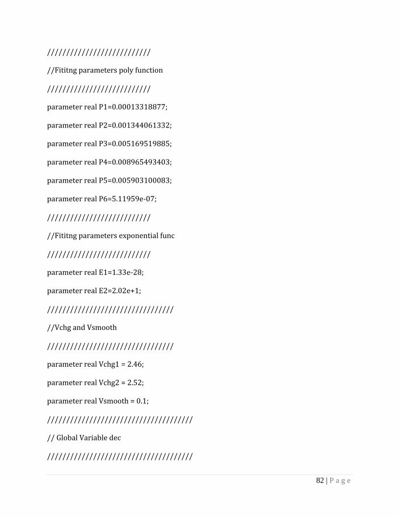
82 | P a g e
///////////////////////////
//Fititng parameters poly function
///////////////////////////
parameter real P1=0.00013318877;
parameter real P2=0.001344061332;
parameter real P3=0.005169519885;
parameter real P4=0.008965493403;
parameter real P5=0.005903100083;
parameter real P6=5.11959e-07;
///////////////////////////
//Fititng parameters exponential func
///////////////////////////
parameter real E1=1.33e-28;
parameter real E2=2.02e+1;
/////////////////////////////////
//Vchg and Vsmooth
/////////////////////////////////
parameter real Vchg1 = 2.46;
parameter real Vchg2 = 2.52;
parameter real Vsmooth = 0.1;
//////////////////////////////////////
// Global Variable dec
//////////////////////////////////////

83 | P a g e
real Vin;
real Iout1;
real Iout2;
//////////////////////////
//Smoothing function
///////////////////////////
analog function real smooth_func;
input Vchg,Vsmooth,Vin;
real Vchg,Vsmooth,Vin;
begin
smooth_func = 0.5 * (1+tanh((Vin - Vchg)/Vsmooth));
end
endfunction
//////////////////////////
//Polynomial function
///////////////////////////
analog function real poly_func;
input P1,P2,P3,P4,P5,P6,Vin;
real P1,P2,P3,P4,P5,P6,Vin;
begin
if(Vin<Vchg1)
begin
poly_func = P6 ;
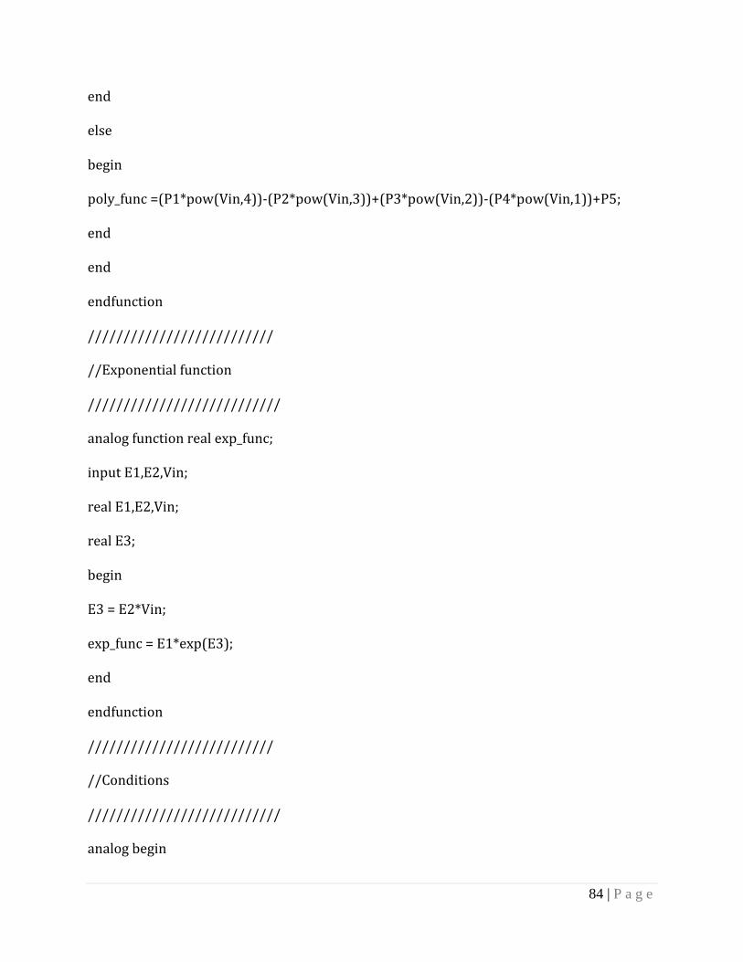
84 | P a g e
end
else
begin
poly_func =(P1*pow(Vin,4))-(P2*pow(Vin,3))+(P3*pow(Vin,2))-(P4*pow(Vin,1))+P5;
end
end
endfunction
//////////////////////////
//Exponential function
///////////////////////////
analog function real exp_func;
input E1,E2,Vin;
real E1,E2,Vin;
real E3;
begin
E3 = E2*Vin;
exp_func = E1*exp(E3);
end
endfunction
//////////////////////////
//Conditions
///////////////////////////
analog begin

85 | P a g e
Vin = V(b1);
Iout1=exp_func(E1,E2,V(b1));
Iout2=(poly_func(P1,P2,P3,P4,P5,P6,V(b1)) * smooth_func(Vchg2,Vsmooth,V(b1))) + ((1-
smooth_func(Vchg2,Vsmooth,V(b1)))*exp_func(E1,E2,V(b1)));
// I=I(b1);
// Iout1=I(b1);
I(b1) <+ Iout2;end
endmodule
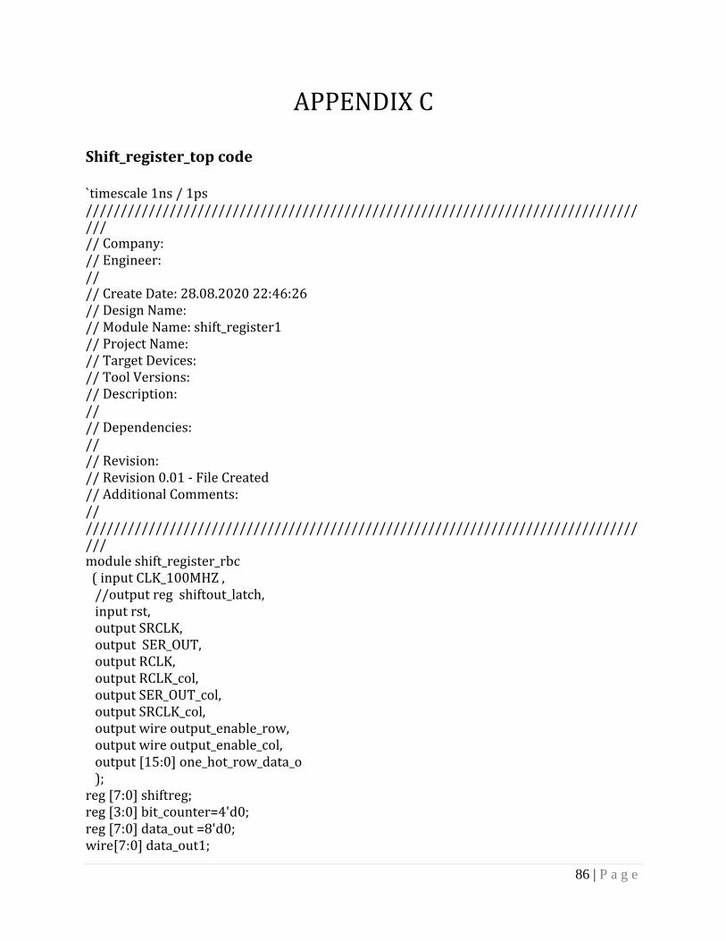
86 | P a g e
APPENDIX C
Shift_register_top code
`timescale 1ns / 1ps ////////////////////////////////////////////////////////////////////////////////// // Company: // Engineer: // // Create Date: 28.08.2020 22:46:26 // Design Name: // Module Name: shift_register1 // Project Name: // Target Devices: // Tool Versions: // Description: // // Dependencies: // // Revision: // Revision 0.01 - File Created // Additional Comments: // ////////////////////////////////////////////////////////////////////////////////// module shift_register_rbc ( input CLK_100MHZ , //output reg shiftout_latch, input rst, output SRCLK, output SER_OUT, output RCLK, output RCLK_col, output SER_OUT_col, output SRCLK_col, output wire output_enable_row, output wire output_enable_col, output [15:0] one_hot_row_data_o ); reg [7:0] shiftreg; reg [3:0] bit_counter=4'd0; reg [7:0] data_out =8'd0; wire[7:0] data_out1;

87 | P a g e
reg [15:0] row_count; wire [15:0] row_data; wire clk_div; reg [2:0] divider; reg [31:0]s_axi_araddr=0; reg s_axi_arvalid; wire s_axi_arready; wire s_axi_awready; wire s_axi_wready; wire [31:0]s_axi_rdata; reg s_axi_rready=0; wire s_axi_rvalid; wire ready; wire rclk; reg rclk_row1; reg rclk_col1; reg rclk_col2; reg rclk_col3; reg rclk_col4; reg rclk_col5; reg rclk_col6; reg rclk_col7; reg rclk_col8; reg oe1; reg oe2; reg oe3; reg oe4; reg oe5; wire rclk_col; wire srclk_col; wire ser_out_col; wire test; reg [15:0] one_hot_row_data; wire[15:0] byte_in; reg enable_sig; reg enable; wire test_reg; reg [4:0] srclk_count; assign RCLK_col=rclk_col1; assign one_hot_row_data_o=one_hot_row_data; blk_mem_gen_0 memory_axi ( .rsta_busy(), // output wire rsta_busy .rstb_busy(), // output wire rstb_busy .s_aclk(clk_div), // input wire s_aclk .s_aresetn(~rst), // input wire s_aresetn .s_axi_awaddr(32'd0), // input wire [31 : 0] s_axi_awaddr
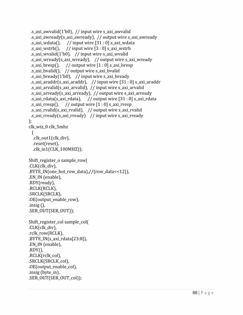
88 | P a g e
.s_axi_awvalid(1'b0), // input wire s_axi_awvalid .s_axi_awready(s_axi_awready), // output wire s_axi_awready .s_axi_wdata(), // input wire [31 : 0] s_axi_wdata .s_axi_wstrb(), // input wire [3 : 0] s_axi_wstrb .s_axi_wvalid(1'b0), // input wire s_axi_wvalid .s_axi_wready(s_axi_wready), // output wire s_axi_wready .s_axi_bresp(), // output wire [1 : 0] s_axi_bresp .s_axi_bvalid(), // output wire s_axi_bvalid .s_axi_bready(1'b0), // input wire s_axi_bready .s_axi_araddr(s_axi_araddr), // input wire [31 : 0] s_axi_araddr .s_axi_arvalid(s_axi_arvalid), // input wire s_axi_arvalid .s_axi_arready(s_axi_arready), // output wire s_axi_arready .s_axi_rdata(s_axi_rdata), // output wire [31 : 0] s_axi_rdata .s_axi_rresp(), // output wire [1 : 0] s_axi_rresp .s_axi_rvalid(s_axi_rvalid), // output wire s_axi_rvalid .s_axi_rready(s_axi_rready) // input wire s_axi_rready ); clk_wiz_0 clk_5mhz ( .clk_out1(clk_div), .reset(reset), .clk_in1(CLK_100MHZ)); Shift_register_o sample_row( .CLK(clk_div), .BYTE_IN(one_hot_row_data),//row_data<<12), .EN_IN (enable), .RDY(ready), .RCLK(RCLK), .SRCLK(SRCLK), .OE(output_enable_row), .insig (), .SER_OUT(SER_OUT)); Shift_register_col sample_col( .CLK(clk_div), .rclk_row(RCLK), .BYTE_IN(s_axi_rdata[23:8]), .EN_IN (enable), .RDY(), .RCLK(rclk_col), .SRCLK(SRCLK_col), .OE(output_enable_col), .insig (byte_in), .SER_OUT(SER_OUT_col));

89 | P a g e
reg [3:0] state=0; always@(posedge clk_div or posedge rst) begin if (rst==1'b1) begin state <= 0; enable<= 0; s_axi_arvalid<=0; s_axi_araddr <=32'd0; s_axi_rready <= 0; end else begin case (state) 0:begin enable<=0; if(ready == 1'b1 && s_axi_arready==1'b1)begin s_axi_arvalid <=1'b1; if (s_axi_araddr == 32'd4096)begin s_axi_araddr<=32'd4; end else begin s_axi_araddr <= s_axi_araddr+32'd4; end state <=1; end else begin s_axi_arvalid <= 1'b0; s_axi_araddr <= s_axi_araddr; state <= 0; end end 1:begin s_axi_arvalid<=1'b0; s_axi_araddr <=s_axi_araddr; if(s_axi_rvalid ==1'b1)begin s_axi_rready <= 1'b1; state <= 2; enable<= 1; end else begin s_axi_rready <= 1'b0; state <= 1; enable<= 0; end end 2:begin

90 | P a g e
s_axi_arvalid<=1'b0; s_axi_araddr <=s_axi_araddr; s_axi_rready <= 1'b0; if(RCLK == 1'b1)begin enable <=0; state <=0; end else begin enable <= 1; state <= 2; end end default: begin s_axi_arvalid<=1'b0; s_axi_araddr <=s_axi_araddr; s_axi_rready <= 1'b0; enable <= 0; state <=0; end endcase end end always@(posedge clk_div or posedge rst) begin if (rst==1'b1)begin rclk_col1 <= 1'b0; rclk_col2 <= 1'b0; rclk_col3 <= 1'b0; rclk_col4 <= 1'b0; rclk_col5 <= 1'b0; rclk_col6 <= 1'b0; rclk_col7 <= 1'b0; rclk_col8 <= 1'b0; end else begin rclk_col1 <= rclk_col; rclk_col2 <= rclk_col1; rclk_col3 <= rclk_col2; rclk_col4 <= rclk_col3; rclk_col5 <= rclk_col4; rclk_col6 <= rclk_col5; rclk_col7 <= rclk_col6; rclk_col8 <= rclk_col7; end end
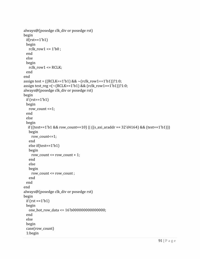
91 | P a g e
always@(posedge clk_div or posedge rst) begin if(rst==1'b1) begin rclk_row1 <= 1'b0 ; end else begin rclk_row1 <= RCLK; end end assign test = ((RCLK==1'b1) && ~(rclk_row1==1'b1))?1:0; assign test_reg =(~(RCLK==1'b1) && (rclk_row1==1'b1))?1:0; always@(posedge clk_div or posedge rst) begin if (rst==1'b1) begin row_count <=1; end else begin if ((test==1'b1 && row_count==10) || ((s_axi_araddr == 32'd4164) && (test==1'b1))) begin row_count<=1; end else if(test==1'b1) begin row_count <= row_count + 1; end else begin row_count <= row_count ; end end end always@(posedge clk_div or posedge rst) begin if (rst ==1'b1) begin one_hot_row_data <= 16'b000000000000000; end else begin case(row_count) 1:begin
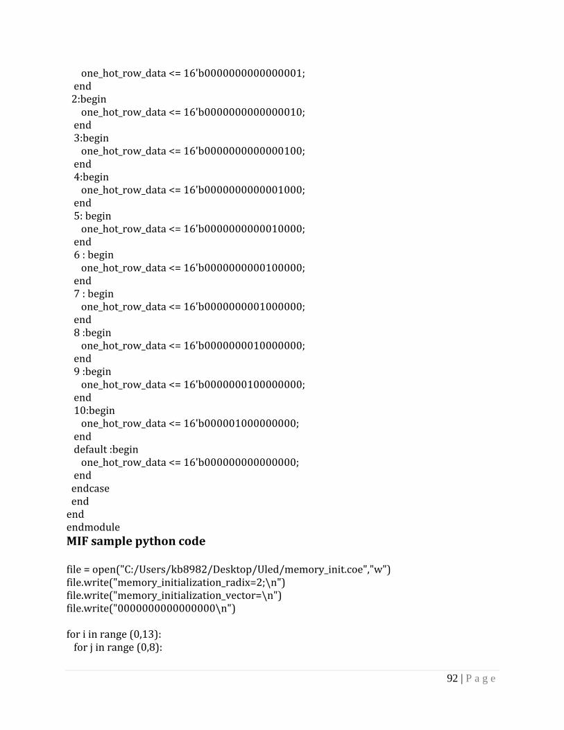
92 | P a g e
one_hot_row_data <= 16'b0000000000000001; end 2:begin one_hot_row_data <= 16'b0000000000000010; end 3:begin one_hot_row_data <= 16'b0000000000000100; end 4:begin one_hot_row_data <= 16'b0000000000001000; end 5: begin one_hot_row_data <= 16'b0000000000010000; end 6 : begin one_hot_row_data <= 16'b0000000000100000; end 7 : begin one_hot_row_data <= 16'b0000000001000000; end 8 :begin one_hot_row_data <= 16'b0000000010000000; end 9 :begin one_hot_row_data <= 16'b0000000100000000; end 10:begin one_hot_row_data <= 16'b000001000000000; end default :begin one_hot_row_data <= 16'b000000000000000; end endcase end end endmodule
MIF sample python code
file = open("C:/Users/kb8982/Desktop/Uled/memory_init.coe","w") file.write("memory_initialization_radix=2;\n") file.write("memory_initialization_vector=\n") file.write("0000000000000000\n") for i in range (0,13): for j in range (0,8):
93 | P a g e
if (j<1): for k in range (0,10): bits=bin(1023)[2:].zfill(16) file.write(bits[::-1] +"\n") else: for l in range (0,10): if(i==12 and j==7 and l==9): bits=bin(0)[2:].zfill(16) file.write(bits[::-1]+";"+"\n") else: bits=bin(0)[2:].zfill(16) file.write(bits[::-1] +"\n") file.close() XDC
# ==== Clock input ==== set_property PACKAGE_PIN E3 [get_ports CLK_100MHZ] set_property IOSTANDARD LVCMOS33 [get_ports CLK_100MHZ] #create_clock -period 125.000 -name sys_clk_pin -waveform 0.000 5.000 -add [get_ports clk] create_clock -period 10.000 -name sys_clk_pin -waveform 0.000 5.000 -add [get_ports CLK_100MHZ] ## ==== Push Button ==== set_property PACKAGE_PIN J15 [get_ports rst] set_property IOSTANDARD LVCMOS33 [get_ports rst] ## ==== Outputs ==== set_property -dict PACKAGE_PIN C17 IOSTANDARD LVCMOS33 [get_ports SRCLK ]; #IO_L20N_T3_A19_15 Sch=ja[1] set_property -dict PACKAGE_PIN D18 IOSTANDARD LVCMOS33 [get_ports SER_OUT ];# IO_L21N_T3_DQS_A18_15 Sch=ja[2] set_property -dict PACKAGE_PIN E18 IOSTANDARD LVCMOS33 [get_ports RCLK ];# IO_L21P_T3_DQS_15 Sch=ja[3] set_property -dict PACKAGE_PIN G17 IOSTANDARD LVCMOS33 [get_ports output_enable_row ]; set_property -dict PACKAGE_PIN D14 IOSTANDARD LVCMOS33 [get_ports SRCLK_col ];# IO_L21P_T3_DQS_15 Sch=jb[1] set_property -dict PACKAGE_PIN F16 IOSTANDARD LVCMOS33 [get_ports SER_OUT_col ];# IO_L21P_T3_DQS_15 Sch=jb[2] set_property -dict PACKAGE_PIN G16 IOSTANDARD LVCMOS33 [get_ports RCLK_col ];# IO_L21P_T3_DQS_15 Sch=jb[3] set_property -dict PACKAGE_PIN H14 IOSTANDARD LVCMOS33 [get_ports output_enable_col ]; ==== LEDs ==== set_property PACKAGE_PIN H17 [get_ports one_hot_row_data_o[0]] set_property IOSTANDARD LVCMOS33 [get_ports one_hot_row_data_o[0]]
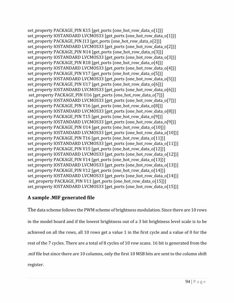
94 | P a g e
set_property PACKAGE_PIN K15 [get_ports one_hot_row_data_o[1]] set_property IOSTANDARD LVCMOS33 [get_ports one_hot_row_data_o[1]] set_property PACKAGE_PIN J13 [get_ports one_hot_row_data_o[2]] set_property IOSTANDARD LVCMOS33 [get_ports one_hot_row_data_o[2]] set_property PACKAGE_PIN N14 [get_ports one_hot_row_data_o[3]] set_property IOSTANDARD LVCMOS33 [get_ports one_hot_row_data_o[3]] set_property PACKAGE_PIN R18 [get_ports one_hot_row_data_o[4]] set_property IOSTANDARD LVCMOS33 [get_ports one_hot_row_data_o[4]] set_property PACKAGE_PIN V17 [get_ports one_hot_row_data_o[5]] set_property IOSTANDARD LVCMOS33 [get_ports one_hot_row_data_o[5]] set_property PACKAGE_PIN U17 [get_ports one_hot_row_data_o[6]] set_property IOSTANDARD LVCMOS33 [get_ports one_hot_row_data_o[6]] set_property PACKAGE_PIN U16 [get_ports one_hot_row_data_o[7]] set_property IOSTANDARD LVCMOS33 [get_ports one_hot_row_data_o[7]] set_property PACKAGE_PIN V16 [get_ports one_hot_row_data_o[8]] set_property IOSTANDARD LVCMOS33 [get_ports one_hot_row_data_o[8]] set_property PACKAGE_PIN T15 [get_ports one_hot_row_data_o[9]] set_property IOSTANDARD LVCMOS33 [get_ports one_hot_row_data_o[9]] set_property PACKAGE_PIN U14 [get_ports one_hot_row_data_o[10]] set_property IOSTANDARD LVCMOS33 [get_ports one_hot_row_data_o[10]] set_property PACKAGE_PIN T16 [get_ports one_hot_row_data_o[11]] set_property IOSTANDARD LVCMOS33 [get_ports one_hot_row_data_o[11]] set_property PACKAGE_PIN V15 [get_ports one_hot_row_data_o[12]] set_property IOSTANDARD LVCMOS33 [get_ports one_hot_row_data_o[12]] set_property PACKAGE_PIN V14 [get_ports one_hot_row_data_o[13]] set_property IOSTANDARD LVCMOS33 [get_ports one_hot_row_data_o[13]] set_property PACKAGE_PIN V12 [get_ports one_hot_row_data_o[14]] set_property IOSTANDARD LVCMOS33 [get_ports one_hot_row_data_o[14]] set_property PACKAGE_PIN V11 [get_ports one_hot_row_data_o[15]] set_property IOSTANDARD LVCMOS33 [get_ports one_hot_row_data_o[15]]
A sample .MIF generated file
The data scheme follows the PWM scheme of brightness modulation. Since there are 10 rows
in the model board and if the lowest brightness out of a 3 bit brightness level scale is to be
achieved on all the rows, all 10 rows get a value 1 in the first cycle and a value of 0 for the
rest of the 7 cycles. There are a total of 8 cycles of 10 row scans. 16 bit is generated from the
.mif file but since there are 10 columns, only the first 10 MSB bits are sent to the column shift
register.
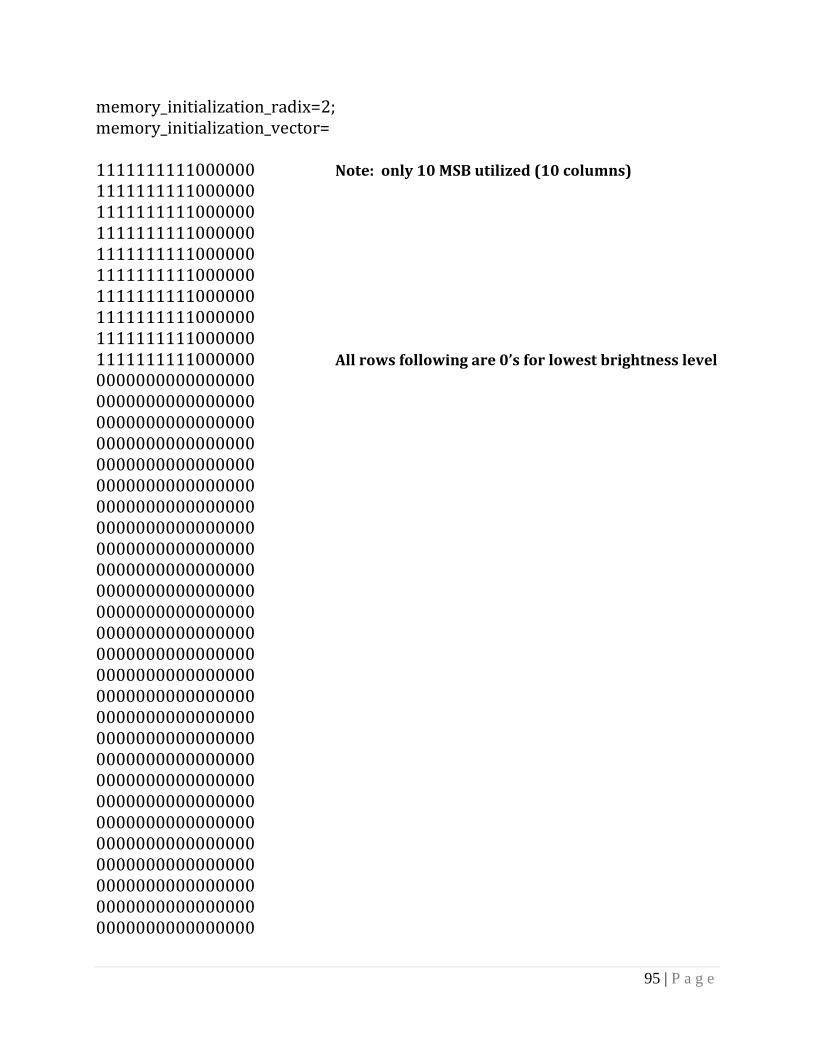
95 | P a g e
memory_initialization_radix=2; memory_initialization_vector=
1111111111000000 Note: only 10 MSB utilized (10 columns)
1111111111000000 1111111111000000 1111111111000000 1111111111000000 1111111111000000 1111111111000000 1111111111000000 1111111111000000 1111111111000000 All rows following are 0’s for lowest brightness level
0000000000000000 0000000000000000 0000000000000000 0000000000000000 0000000000000000 0000000000000000 0000000000000000 0000000000000000 0000000000000000 0000000000000000 0000000000000000 0000000000000000 0000000000000000 0000000000000000 0000000000000000 0000000000000000 0000000000000000 0000000000000000 0000000000000000 0000000000000000 0000000000000000 0000000000000000 0000000000000000 0000000000000000 0000000000000000 0000000000000000 0000000000000000

96 | P a g e
0000000000000000 0000000000000000 0000000000000000 0000000000000000 0000000000000000 0000000000000000 0000000000000000 0000000000000000 0000000000000000 0000000000000000 0000000000000000 0000000000000000 0000000000000000 0000000000000000 0000000000000000 0000000000000000 0000000000000000 0000000000000000 0000000000000000 0000000000000000 0000000000000000 0000000000000000 0000000000000000 0000000000000000 0000000000000000 0000000000000000 0000000000000000 0000000000000000 0000000000000000 0000000000000000 0000000000000000 0000000000000000 0000000000000000 0000000000000000 0000000000000000 0000000000000000 0000000000000000 0000000000000000 0000000000000000 0000000000000000

97 | P a g e
0000000000000000 0000000000000000 0000000000000000;

98 | P a g e

99 | P a g e