Embed Size (px)
Citation preview
BFF1303: ELECTRICAL /
ELECTRONICS ENGINEERING
Analog Electronics:
BJT Biasing Circuits
Ismail Mohd Khairuddin , Zulkifil Md Yusof
Faculty of Manufacturing Engineering Universiti Malaysia Pahang

2
I Mohd-Khairuddin , Z Md-Yusof
BFF1303 Electrical/Electronic Engineering 2
Faculty of Manufacturing Universiti Malaysia Pahang
Kampus Pekan, Pahang Darul Makmur Tel: +609-424 5800 Fax: +609-4245888
http://fkp.ump.edu.my/
Bipolar Junction
Transistor-DC Biasing
BFF1303 ELECTRICAL/ELECTRONICS ENGINEERING
Contents:
Outcomes
Operating Point
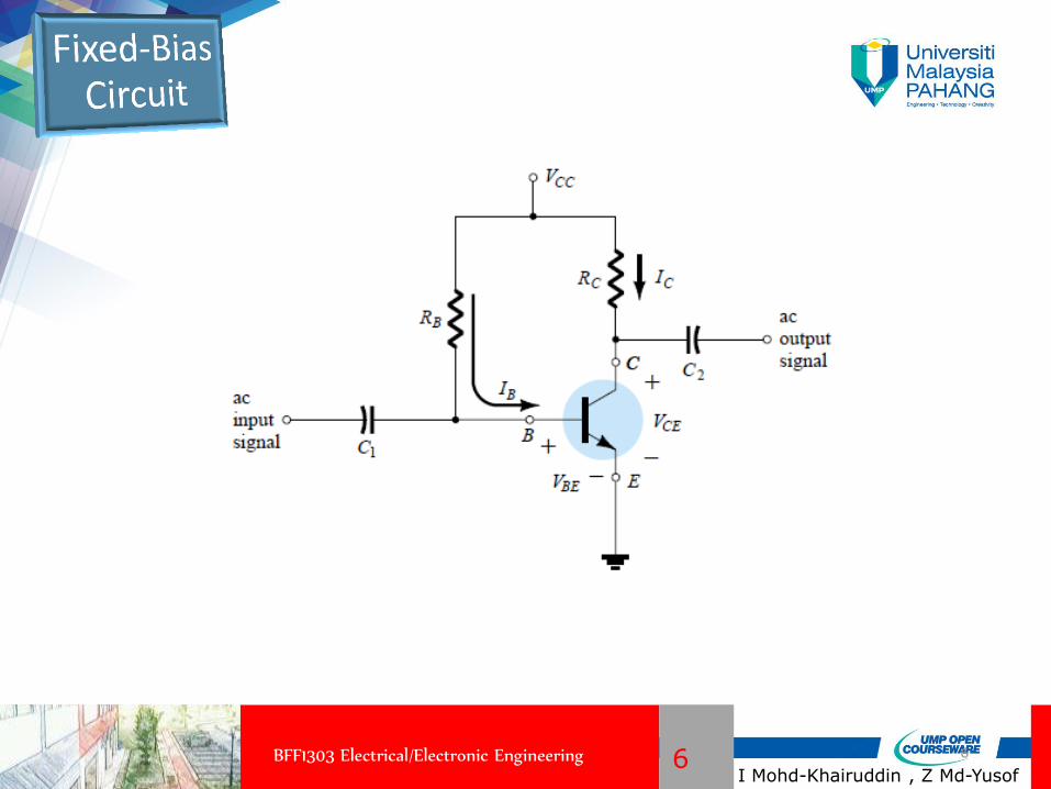
Fixed-Bias Circuit
Emitter Bias
Voltage-Divider Bias
DC Bias with Voltage Feedback
Design Operations
Transistor Switching Network
PNP Transistor

3
I Mohd-Khairuddin , Z Md-Yusof
BFF1303 Electrical/Electronic Engineering 3
Understand the physical operation of bipolar
transistor
Select the operating point of a bipolar transistor circuit
Compute performance of several important
amplifier configurations.
Select an amplifier configuration appropriate
for a given application.

4
I Mohd-Khairuddin , Z Md-Yusof
BFF1303 Electrical/Electronic Engineering 4
Biasing: The DC voltages applied to a transistor in order to turn it on so that it can amplify the AC signal.
The DC input establishes an operating or quiescent point called the Q-point.

5
I Mohd-Khairuddin , Z Md-Yusof
BFF1303 Electrical/Electronic Engineering 5
Active or Linear Region Operation Base–Emitter junction is forward biased Base–Collector junction is reverse biased
Cutoff Region Operation
Base–Emitter junction is reverse biased
Saturation Region Operation
Base–Emitter junction is forward biased Base–Collector junction is forward biased
6
I Mohd-Khairuddin , Z Md-Yusof
BFF1303 Electrical/Electronic Engineering 6

7
I Mohd-Khairuddin , Z Md-Yusof
BFF1303 Electrical/Electronic Engineering 7
Base-Emitter Loop
From Kirchhoff’s voltage law:
Solving for base current:
+VCC – IBRB – VBE = 0
CC BEB
B
V VI
R
8
I Mohd-Khairuddin , Z Md-Yusof
BFF1303 Electrical/Electronic Engineering 8
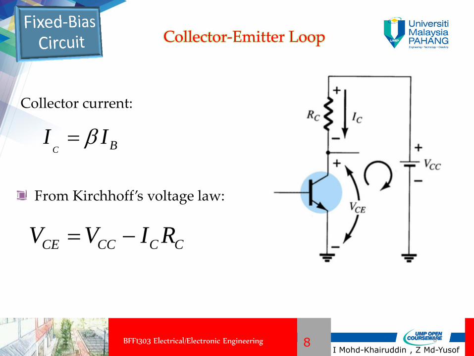
Collector-Emitter Loop
Collector current:
From Kirchhoff’s voltage law:
C BI I
CE CC C CV V I R

9
I Mohd-Khairuddin , Z Md-Yusof
BFF1303 Electrical/Electronic Engineering 9
240k
2.2k
12V
10 F
10 F
50
Determine the following for the fixed-bias configuration of figure shown
, , , , ,B C CE B C BCI I V V V V

10
I Mohd-Khairuddin , Z Md-Yusof
BFF1303 Electrical/Electronic Engineering 10
Solution
Apply KVL to Base-Emitter loop,
0CC B B BEV R I V
Then CC BEB
B
V VI
R
12 0.747.08 A
240kBI
Collector current:
2.35mAC BI I
Apply KVL to Collector-Emitter loop,
6.83V
CE CC C C
CE
V V I R
V
0.7 V
6.83V
B BE
C CE
V V
V V
6.13V
BC B C
BC
V V V
V
11
I Mohd-Khairuddin , Z Md-Yusof
BFF1303 Electrical/Electronic Engineering 11
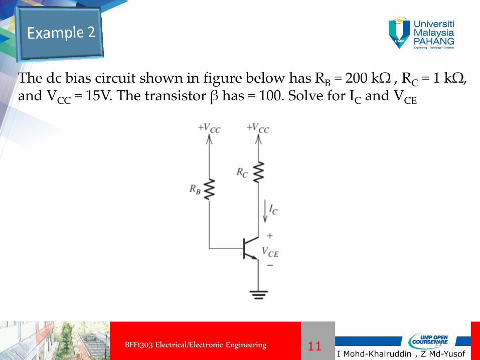
The dc bias circuit shown in figure below has RB = 200 kΩ , RC = 1 kΩ, and VCC = 15V. The transistor β has = 100. Solve for IC and VCE

12
I Mohd-Khairuddin , Z Md-Yusof
BFF1303 Electrical/Electronic Engineering 12
Solution
Apply KVL to Base-Emitter loop,
0CC B B BEV R I V
CC BEB
B
V VI
R
15 0.771.5 A
200kBI
Collector current:
100 71.5
7.15mA
C B
C
C
I I
I
I
Apply KVL to Collector-Emitter loop,
15 7.15 1k 7.85V
CE CC C C
CE
V V I R
V
13
I Mohd-Khairuddin , Z Md-Yusof
BFF1303 Electrical/Electronic Engineering 13
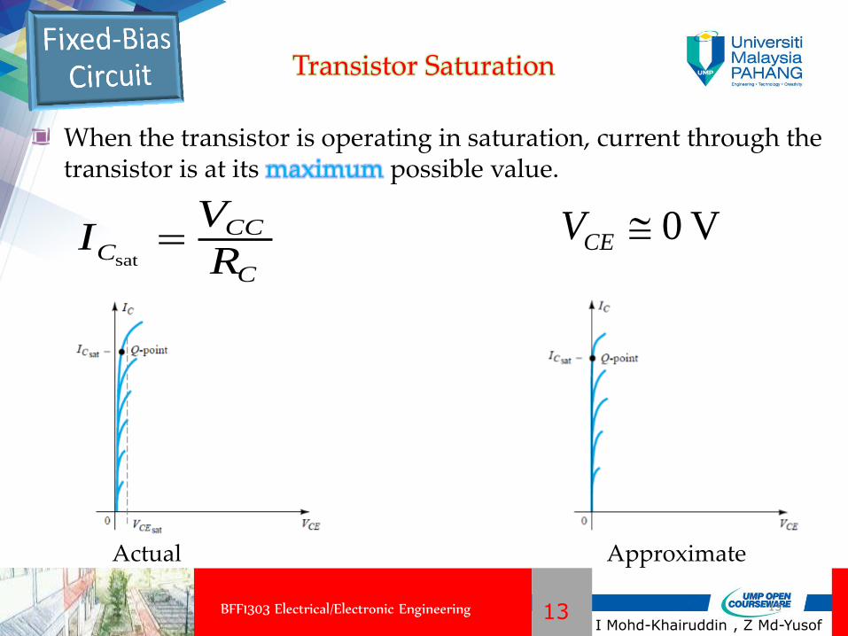
Transistor Saturation
When the transistor is operating in saturation, current through the transistor is at its maximum possible value.
sat
CCC
C
VI
R 0 VCEV
Actual Approximate

14
I Mohd-Khairuddin , Z Md-Yusof
BFF1303 Electrical/Electronic Engineering 14
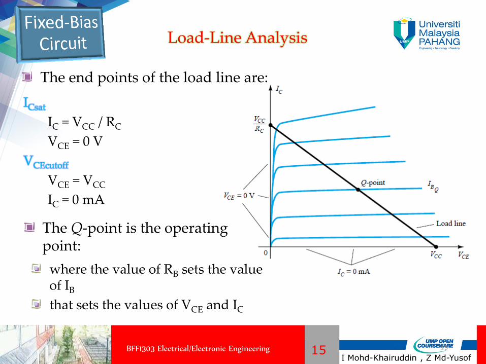
Load-Line Analysis
15
I Mohd-Khairuddin , Z Md-Yusof
BFF1303 Electrical/Electronic Engineering 15
Load-Line Analysis
ICsat
IC = VCC / RC
VCE = 0 V
VCEcutoff
VCE = VCC
IC = 0 mA
where the value of RB sets the value of IB
that sets the values of VCE and IC
The Q-point is the operating point:
The end points of the load line are:
16
I Mohd-Khairuddin , Z Md-Yusof
BFF1303 Electrical/Electronic Engineering 16
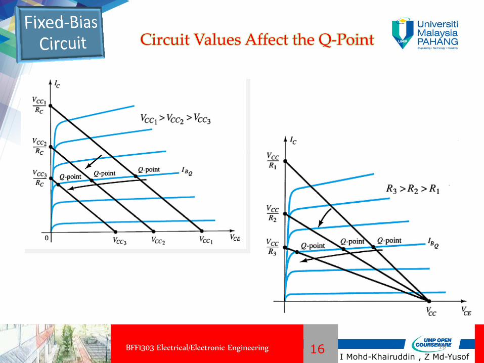
Circuit Values Affect the Q-Point

17
I Mohd-Khairuddin , Z Md-Yusof
BFF1303 Electrical/Electronic Engineering 17
Circuit Values Affect the Q-Point

18
I Mohd-Khairuddin , Z Md-Yusof
BFF1303 Electrical/Electronic Engineering 18
Adding a resistor (RE) to the emitter circuit stabilizes the bias circuit.

19
I Mohd-Khairuddin , Z Md-Yusof
BFF1303 Electrical/Electronic Engineering 19
Base-Emitter Loop
From Kirchhoff’s voltage law:
( 1) 0CC B B B EV I R I R
0CC B B BE E EV I R V I R
( 1)
CC BEB
B E
V VI
R R
Since IE = (β + 1)IB:
Solving for IB:

20
I Mohd-Khairuddin , Z Md-Yusof
BFF1303 Electrical/Electronic Engineering 20
Collector-Emitter Loop
From Kirchhoff’s voltage law:
CE CC C C EV V I R R
0E E CE C C CCI R V I R V
E E E
C CE E CC C C
B CC R B BE E
V I R
V V V V I R
V V I R V V
Since IE IC :
Also:

21
I Mohd-Khairuddin , Z Md-Yusof
BFF1303 Electrical/Electronic Engineering 21
Improved Biased Stability
Stability refers to a circuit condition in which the currents and voltages will remain fairly constant over a wide range of temperatures and transistor Beta (β) values.
Adding RE to the emitter improves the stability of a transistor.
Saturation Level
The endpoints can be determined from the load line.
VCEcutoff : ICsat:
0 mA
CE CC
C
V V
I
0 VCE
CCC
C E
V
VI
R R

22
I Mohd-Khairuddin , Z Md-Yusof
BFF1303 Electrical/Electronic Engineering 22
This is a very stable bias circuit.
The currents and voltages are nearly independent of any variations in β.

23
I Mohd-Khairuddin , Z Md-Yusof
BFF1303 Electrical/Electronic Engineering 23
Approximate Analysis
Where IB << I1 and I1 I2 :
Where βRE > 10R2:
From Kirchhoff’s voltage law:
2
1 2
CCB
R VV
R R
EE
E
E B BE
VI
R
V V V
CE CC C C E EV V I R I R ( )
E C
CE CC C C E
I I
V V I R R

24
I Mohd-Khairuddin , Z Md-Yusof
BFF1303 Electrical/Electronic Engineering 24
Another way to improve the stability of a bias circuit is to add a feedback path from collector to base.
In this bias circuit the Q-point is only slightly dependent on the transistor beta, β.

25
I Mohd-Khairuddin , Z Md-Yusof
BFF1303 Electrical/Electronic Engineering 25
Base-Emitter Loop
( )
CC BEB
B C E
V VI
R R R
From Kirchhoff’s voltage law:
' – – – – 0CC C C B B BE E EV I R I R V I R
Where IB << IC:
'
C C B CI I I I
Knowing IC = IB and IE IC, the loop equation becomes:
– 0CC B C B B BE B EV I R I R V I R
Solving for IB:

26
I Mohd-Khairuddin , Z Md-Yusof
BFF1303 Electrical/Electronic Engineering 26
Base-Emitter Bias Analysis
Transistor Saturation Level
EC
CCCmaxCsat
RR
VII
Load Line Analysis
Cutoff: Saturation:
mA 0I
VV
C
CCCE
V 0VCE
ER
CR
CCV
CI

27
I Mohd-Khairuddin , Z Md-Yusof
BFF1303 Electrical/Electronic Engineering 27
The analysis for pnp transistor biasing circuits is the same as that for npn transistor circuits. The only difference is that the currents are flowing in the opposite direction.