Embed Size (px)
Citation preview

Bipolar Junction Transistor (BJT) - Introduction
It was found in 1948 at the Bell Telephone Laboratories.
It is a three terminal device and has three semiconductorregions.
It can be used in signal amplification and digital logic circuitsas well.
Its current conduction process is due to both holes andelectrons. That is why the name bipolar.
S. Sivasubramani EE101 - BJT 1/ 60

NPN Transistor
E C
B
n type p type n type
Emitter region Base region Collector region
EB Junction CB Junction
B
C
E
Figure: Symbol
S. Sivasubramani EE101 - BJT 2/ 60

PNP Transistor
E C
B
p type n type p type
Emitter region Base region Collector region
EB Junction CB Junction
B
C
E
Figure: Symbol
S. Sivasubramani EE101 - BJT 3/ 60

BJT - Modes of Operation
Mode EB Junction CB Junction
Active Forward Reverse
Saturation Forward Forward
Cutoff Reverse Reverse
Active mode - Amplification
Saturation and Cutoff - Digital logic circuits
S. Sivasubramani EE101 - BJT 4/ 60

Active Mode - NPN Transistor
E IE C
IC
B
IB
N P N
Emitter Base Collector
VBE VCB
iC = IS exp(vBEVt
)
iB =iCβ
where β is common-emitter current gain.Its typical value is in the range of 50 to 200.
S. Sivasubramani EE101 - BJT 5/ 60

Active Mode
By KCLiE = iC + iB
iE = iCβ + 1
β
iC = αiE
where α is a constant.
α =β
β + 1
iE =ISαexp(
vBEVt
)
If β = 100, then α ≈ 0.99. α is called as common-base currentgain.
S. Sivasubramani EE101 - BJT 6/ 60

i − v Characteristics - CE
VBE
IB
VCE
IC
IE
vBE (V)
iB
0.5 0.7
S. Sivasubramani EE101 - BJT 7/ 60

i − v Characteristics - CE
vCE
iC
vBE = · · ·
vBE = · · ·
vBE = · · ·
vBE = · · ·
Active Region
Saturation Region
Cutoff Region
As long as vCE > vCE sat , BJT is in active region. vCE sat = 0.2 V.If vCE falls below vCE sat , BJT will enter into saturation region.
S. Sivasubramani EE101 - BJT 8/ 60

BJT Model - Active Mode
BiB
+
−
vBE
iE
E
CiC
βiB
This model is nonlinear. (large signal)As E is common to both input and output, it is called as commonemitter configuration.
S. Sivasubramani EE101 - BJT 9/ 60

i − v Characteristics - Practical BJT
Date/Time run: 09/16/14 17:20:34* C:\IITP\Academic_Work\Subjects_Taken\2014\EE101\PSPICE\BJT_Characteristics.sch
Temperature: 27.0
Date: September 16, 2014 Page 1 Time: 17:22:04
(A) BJT_Characteristics (active)
V_V2
0V 5V 10VIC(Q1)
0A
0.5A
1.0A
S. Sivasubramani EE101 - BJT 10/ 60

Early Voltage
As Practical BJTs have finite slope in the iC Vs vCE characteristicswhile acting in active mode.This is accounted for by the following relation.
iC = IS exp(vBEVt
)(1 +vCEVA
)
where VA is the Early voltage whose value is in the range of 10 Vto 100 V.The nonzero slope indicates the output resistance is finite.
S. Sivasubramani EE101 - BJT 11/ 60

Large Signal Model Including Early Voltage
BiB
+
−
vBE
iE
E
CiC
βiB ro
It is the large signal model of common emitter NPN transistor inactive region. As there is no restriction in the signal range, it iscalled as a large signal model.
S. Sivasubramani EE101 - BJT 12/ 60

Summary - Active Mode
iC = IS exp(vBEVt
)
iB =iCβ
=ISβ
exp(vBEVt
)
iE =iCα
=ISα
exp(vBEVt
)
iC = βiB ; iC = αiE
α =β
β + 1
β =α
α− 1
S. Sivasubramani EE101 - BJT 13/ 60

BJT - Various Modes of Operation
IB
IC
+
−VBE
+
−VBC +
−
VCE
VBE = VBC + VCE
VBC = VBE − VCE
1 Active mode : VBE = 0.7V , VCE > 0.2V .
2 Saturation mode : VBE = 0.7V , VCE ≤ 0.2V .
3 Cutoff mode: VBE < 0.5V , VBC < 0.5V .
S. Sivasubramani EE101 - BJT 14/ 60

BJT Models - Active Mode
B
E
CiC
βiB
IB > 0
+
−
VBE =0.7 V
+
−
VCE >0.2 V
EBJ : Forward biasedCBJ: Reverse biased
S. Sivasubramani EE101 - BJT 15/ 60

BJT Models - Saturation Mode
B
E
CiC
IB > 0
+
−
VBE =0.7 V
+
−
VCE =0.2 V
EBJ : Forward biasedCBJ: Forward biased
S. Sivasubramani EE101 - BJT 16/ 60

BJT Models - Cutoff Mode
B
E
CIB = 0 IC = 0
+
−
VBE< 0.5 V
EBJ : Reverse biasedCBJ: Reverse biased
S. Sivasubramani EE101 - BJT 17/ 60

BJT - DC Analysis
Whenever we want to analyze BJT circuits only with DC voltages,use the following steps.
1 Assume that the transistor is operating in active mode.
2 Determine IC , IB , VCE and VBE using the active mode model.
3 Check for consistency of results with active-mode operationsuch as VCE > VCE sat .
4 If it is satisfied, analysis is over.
5 If not, assume saturation mode and repeat the analysis likeactive mode.
This analysis is mainly used to identify the operating point.
S. Sivasubramani EE101 - BJT 18/ 60

Check yourself
Which mode is transistor operating? β=100 and VBE = 0.7 V.
4 V
4.7 k Ω
10 V
3.3 kΩ
By KVL in Base Emitter loop,
4 = VBE + 3.3IE
IE = 1 mA
IB =IE
β + 1=
1
101= 9.9µA
IC = IE − IB = 0.99 mA
By KVL in CE loop,
VCE = 10−4.7× IC −3.3× IE = 2.047 V
Since VCE > VCE sat , it is operating inactive mode.
S. Sivasubramani EE101 - BJT 19/ 60

Amplifier - An Introduction
io
RL
+
−
vO(t)
iI
vI (t)
vI (t)vO(t)
S. Sivasubramani EE101 - BJT 20/ 60

Amplifier - An Introduction
vO(t) = AvI (t)
As vO and vI are linearly related, it is called as a linear amplifier.
vI
vO
← Slope= A
S. Sivasubramani EE101 - BJT 21/ 60

Amplifier - An Introduction
io
RL
+
−
vO(t)
iI
vI (t)
An amplifier takes power from battery to amplify the signal givenat its input. This is how it amplifies the input signal.
S. Sivasubramani EE101 - BJT 22/ 60

BJT- Amplifier
+−vBE
RC
iC
VCC
+
−
vCE
vBE is the input voltage.RC is the load resistance.The output vCE is taken betweenthe collector and ground.
vCE = VCC − iCRC
vCE = VCC − IS exp(vBEVt
)RC
S. Sivasubramani EE101 - BJT 23/ 60

BJT - Voltage Transfer Characteristics (VTC)
vBE
vCE
0.5 V
0.2 V
Cutoff SaturationActive
S. Sivasubramani EE101 - BJT 24/ 60

BJT - Voltage Transfer Characteristics
Date/Time run: 09/20/14 10:49:03* C:\IITP\Academic_Work\Subjects_Taken\2014\EE101\PSPICE\BJT_Characteristics.sch
Temperature: 27.0
Date: September 20, 2014 Page 1 Time: 10:50:58
(A) BJT_Characteristics (active)
V_V1
0V 0.5V 1.0V 1.5VV(Q1:c)
0V
2.5V
5.0V
S. Sivasubramani EE101 - BJT 25/ 60

BJT - Biasing
VBE
RC
IC
VCC
+
−
VCE vBE
vCE
VCE Q ← Quiescent
VBE
point
VCE = VCC − IS exp(VBE
Vt)RC
S. Sivasubramani EE101 - BJT 26/ 60

BJT- Amplifier
VBE
vbe +
−
vBE
RC
iC
VCC
+
−
vCE
S. Sivasubramani EE101 - BJT 27/ 60

BJT-Amplifier
vBE
vCE
Y
0.5 V
Z0.2 V
Cutoff SaturationActive
VCE Q
VBE
S. Sivasubramani EE101 - BJT 28/ 60

Small Signal Voltage Gain
If the input signal vbe is very small, the output signal vce will be
vce = Avvbe
where Av is the voltage gain that is determined by evaluating theslope of VTC at Q point.
Av =dvcedvbe
∣∣∣VBE
Av =d(VCC − IS exp(
vBEVt
)RC )
dvbe
∣∣∣VBE
=−IS exp(
VBE
Vt)RC
Vt
Av =−ICRC
Vt
S. Sivasubramani EE101 - BJT 29/ 60

Graphical Analysis - To determine Bias point
+−vBE
RC
iC
VCC
+
−
vCE
vCE
iC
vBE = · · ·
vBE = · · ·
vBE = · · ·
vBE = · · ·
VCC
RC
VCC
←i C
=
V CC−v C
E
R C
Z
Q
Y
VCE
IC
S. Sivasubramani EE101 - BJT 30/ 60

How to choose a bias point
There are mainly two factors that determine the location of Q orbias or Operating point.
1 Gain
2 Swing limit at the output
It is clear from graphical analysis, there are three operating points(Z, Q & Y).
If we choose Z, gain will be more but distorted negativeportion of signal.
If we choose Y, reduction in gain and distortion in positiveportion of signal.
If Q is chosen, gain as well as swing in the output signal areachieved.
Choose an operating point that should give gain andmaximum swing
S. Sivasubramani EE101 - BJT 31/ 60

Check yourself
Find the operating point. Assume VBE = 0.7 V.
+
−
vi
500 Ω
VCC = 5V
+
−
vo
215 kΩ
VCE (V)
IC (mA)
IB = 50µA
IB = 40µA
IB = 30µA
IB = 20µA
IB = 10µA2
4
6
8
10
1 2 3 4 5
S. Sivasubramani EE101 - BJT 32/ 60

Solution
5 V
215 kΩ
500 Ω
5 V
By KVL in BE loop,
5 = IB215× 103 + VBE
IB =5− 0.7
215× 103= 20µA
KVL in CE loop, (Load line)
5 = IC500 + VCE
IC =5− VCE
500
S. Sivasubramani EE101 - BJT 33/ 60

Solution - contd...
VCE (V)
IC (mA)
IB = 50µA
IB = 40µA
IB = 30µA
IB = 20µA
IB = 10µA2
4
6
8
10
1 2 3 4 5
QICQ
VCEQ
S. Sivasubramani EE101 - BJT 34/ 60

Transistor Biasing
Biasing means establishing a constant current in the collectorof BJT.
The Q point or bias or Operating point should not besensitive to temperature variations and variations in β.
The location of DC bias point should allow for maximumoutput signal swing.
Transistor is operated in active region by biasing. To calculate ICand VCE corresponding to DC bias, DC analysis should be carriedout.
(Instead of using two different batteries, one DC battery VCC canbe used for both EB and CB junctions.)
S. Sivasubramani EE101 - BJT 35/ 60

Two Basic Schemes - Not to be used
IB
RB2
RB1
VCC
RC
IC
VCC
VCE
+
−VBE
(a)
IB
RB
VCC
RC
IC
VCC
VCE
+
−VBE
(b)
Figure: Bad SchemesS. Sivasubramani EE101 - BJT 36/ 60

Bad Schemes
1 First scheme (Figure a)
It applies constant VBE through voltage divider action.For a small change in VBE due to temperature variation, IBchanges drastically because of exponential relationship betweenthem.It will change IC as IC = βIB .Hence, It is not a good approach.
2 Second scheme (Figure b)
Figure b applies constant IB .If there is a change in β, IC will change.Hence, It is also not a good approach
As these two schemes are sensitive to variation in temperature andvariation in β, they should not be used for biasing a transistor.
S. Sivasubramani EE101 - BJT 37/ 60

Classical Biasing Scheme
IB
R2
R1
VCC
RC
IC
VCC
VCE
RE
+
−VBE
In order to make biasingscheme insensitive totemperature and βvariations, RE is included inemitter circuit.
S. Sivasubramani EE101 - BJT 38/ 60

Classical Bias Scheme - Thevenin Equivalent
IB
VBB = VCCR2
R1 + R2
RC
IC
VCC
VCE
RE
+
−VBE
RB = R1||R2
S. Sivasubramani EE101 - BJT 39/ 60

Classical Bias Scheme
The current IE can be determined by writing KVL in base-emitterloop.
VBB = IBRB + VBE + IERE
Substituting IB =IE
β + 1
VBB = IERB
β + 1+ VBE + IERE
IE =VBB − VBE
RE + RB/(β + 1)
As IC = αIE and α =β
β + 1
IC =β(VBB − VBE )
RE (β + 1) + RB
S. Sivasubramani EE101 - BJT 40/ 60

Contd...
If we choose RE (β + 1) >> RB ,
IC ≈β(VBB − VBE )
RE (β + 1)
Normally β lies in the range of 10 to 100.
β + 1 ≈ β
IC can be written as
IC ≈(VBB − VBE )
RE
Now IC is independent of β. As VBB >> VBE , change in VBE willalso not affect IC much. In this bias scheme, Q point is insensitiveto variation in β and variation in temperature.
S. Sivasubramani EE101 - BJT 41/ 60

Transistor - Small Signal Analysis
To perform small signal analysis, small signal equivalent circuitshould be drawn.
1 Calculate the operating point using DC analysis Click here to refer .
2 Draw the small signal equivalent circuit at this operatingpoint.
3 As small signal circuit is linear, calculating the voltage,current would be easy.
Small signal analysis is also called as ac analysis.
S. Sivasubramani EE101 - BJT 42/ 60

Circuit with small signal
Let us consider this circuit to draw small signal equivalent andanalyze.
VBE
vbe
+
−
vBE
RC
iC
+
−
vCE
VCC
S. Sivasubramani EE101 - BJT 43/ 60

Circuit with small signal - DC Analysis
To find the operating point by DC analysis, ac signal should beremoved.
IB
VBE
RC
IC
IE
+
−
VCE
VCC
Calculate IC , VCE as follows.
IC = IS exp(VBE
Vt)
VCE = VCC − ICRC
Mostly IC is determined as
IC = βIB
where IB is found using KVL inbase emitter loop.
S. Sivasubramani EE101 - BJT 44/ 60

Small signal model - BJT
(refer lecture notes on two port network)Let us consider BJT as a two port network with emitter as acommon terminal.
E−
+
vBE
B iB
−
+
vCE
C
iC
iC = IS exp(vBEVt
)
iB =iCβ
S. Sivasubramani EE101 - BJT 45/ 60

The small signal voltages and currents are related by linearequations.
ib = ybbvbe + ybcvce
ic = ycbvbe + yccvce
As iB and iC are only function of vBE , ybc and ycc will be zero.
ybb =∂iB∂vBE
∣∣∣VBE
=ISβVt
exp(VBE
Vt) =
ICβVt
ycb =∂iC∂vBE
∣∣∣VBE
=ICVt
S. Sivasubramani EE101 - BJT 46/ 60

Bib
rπ
EE
Cic
gmvbe
+
−
vce
+
−
vbe
where rπ =1
ybb=βVt
ICis the resistance between base and emitter
and gm = ycb =ICVt
is the transconductance .
S. Sivasubramani EE101 - BJT 47/ 60

Small signal model - circuit
VBE
vbe
+
−
vBE
RC
iC
+
−
vCE
VCC
Bib
rπ
EE
Cgmvbe
RC
+
−
vce
+
−
vbe
S. Sivasubramani EE101 - BJT 48/ 60

Transistor Small Signal Analysis - Steps to be followed
1 Eliminate the signal source and determine the DC operatingpoint in particular IC and VCE .
2 Calculate the value of small signal model parameters rπ andgm at the operating point.
3 Draw the small signal equivalent circuit by short circuiting theDC sources and open circuiting the DC current sources.
4 Analyze this circuit to determine voltage gain, input resistanceand output resistance.
S. Sivasubramani EE101 - BJT 49/ 60

Example - Small signal analysis
Calculate small signal gainvovi
. Assume β = 100.
100 kΩ
3 V
vi
3 kΩ
VO + vo
10 V
S. Sivasubramani EE101 - BJT 50/ 60

Example - Solution
DC Analysis:
100 kΩ
3 V
3 kΩ
10 V
Assume VBE =0.7 V.
IB =3− 0.7
100× 103
IB = 0.023 mA
IC = βIB = 2.3 mA
VCE = VCC − ICRC = 3.1 V
S. Sivasubramani EE101 - BJT 51/ 60

Solution - Contd
Small signal analysis (AC analysis):
vi
B
100 kΩ
rπ
+
−
vbe
EE
C
gmvbe 3 kΩ
+
−
vo
gm =ICVt
=2.3
25= 0.092f
rπ =β
gm=
100
0.092= 1086.96 Ω
vbe = virπ
100kΩ + rπ= 0.0108vi
vo = −gmvbe × 3000 = −2.96vivovi
= −2.96
S. Sivasubramani EE101 - BJT 52/ 60

AC Coupling
It is used to add input signal to the amplifier and outputsignal to the load without affecting bias point.
It is done with the help of large capacitance.
Large capacitance will become an open circuit in DC analysis.
Large capacitance will behave like a short circuit at signalfrequency in ac analysis.
In addition to two capacitances, one more capacitance is connectedacross RE . It is called as a bypass capacitor which will act as ashort circuit and ground emitter without RE in ac analysis.
S. Sivasubramani EE101 - BJT 53/ 60

CE Amplifier - Example
R2
R1RC
VCC
C2
RL
+
−
vo
RE CE
vi
RSC1
S. Sivasubramani EE101 - BJT 54/ 60

CE Amplifier - DC Analysis
To find the operating point, the circuit is redrawn like this.
R2
R1
RC
IC
VCC
C
REE
+
−
VCE
S. Sivasubramani EE101 - BJT 55/ 60
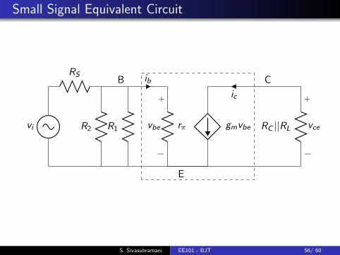
Small Signal Equivalent Circuit
B ib
rπ
+
−
vbe
E
C
ic
gmvbe RC ||RL
+
−
vcevi
RS
R2 R1
S. Sivasubramani EE101 - BJT 56/ 60

BJT - Digital Logic
1 Saturation : When EB junction and CB junction are forwardbiased, BJT will act as a closed switch between collector andemitter.
2 Cutoff : When EB junction and CB junction are reversebiased, BJT will act as an open circuit between collector andemitter.
The above two modes can be used to implement logic functions.
S. Sivasubramani EE101 - BJT 57/ 60

BJT - NOT Gate
RB
Vin
RC
VCC=5 V
Vout
When Vin < 0.7 V (Low), EBand CB junctions are reversebiased. IB = 0, IC = 0.
Vout = VCC = 5V (High)
When Vin = 5 V (High), EB andCB Junctions are forward biased.
Vout = VCEsat = 0.2V (Low)
S. Sivasubramani EE101 - BJT 58/ 60

Check yourself
RB
A
RC
VCC=5 V
C
RB
B
Positive Logic :0 V - Low ”0”5 V - High ”1”
A B C
0 0 10 1 11 0 11 1 0
NAND Gate
S. Sivasubramani EE101 - BJT 59/ 60

Check yourself
RB
A
RE
VCC=5 V
C
RB
B
Positive Logic :0 V - Low ”0”5 V - High ”1”
A B C
0 0 00 1 01 0 01 1 1
AND Gate
S. Sivasubramani EE101 - BJT 60/ 60