Embed Size (px)
Citation preview
7/27/2019 Bjt Basics 1
http://slidepdf.com/reader/full/bjt-basics-1 1/69
Dr. D G Borse
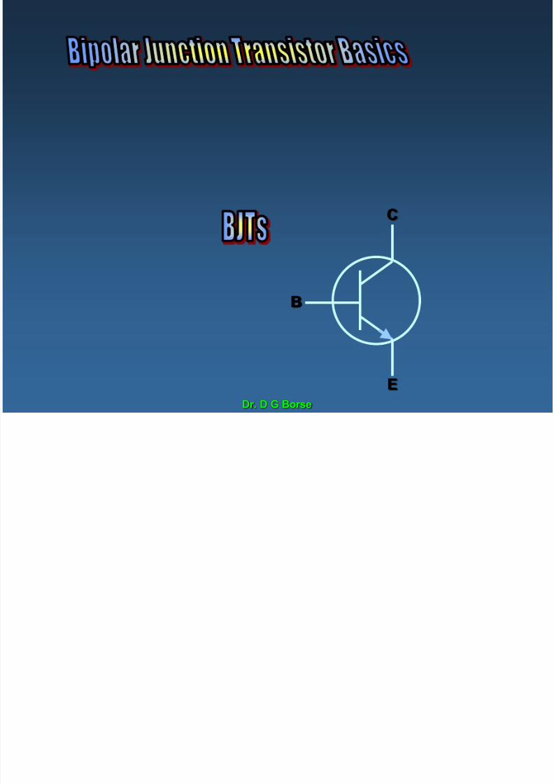
B
C
E
7/27/2019 Bjt Basics 1
http://slidepdf.com/reader/full/bjt-basics-1 2/69
Dr. D G Borse
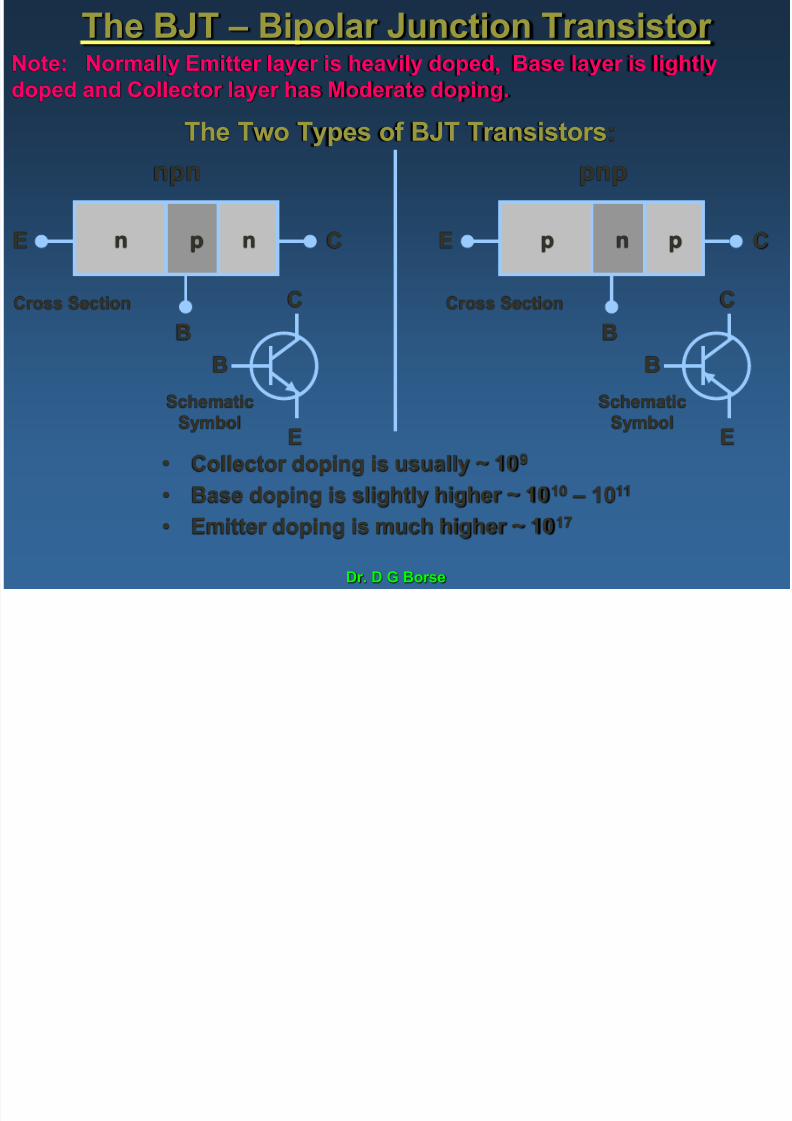
The BJT – Bipolar Junction Transistor
Note: Normally Emitter layer is heavily doped, Base layer is lightly
doped and Collector layer has Moderate doping.
The Two Types of BJT Transistors:npn pnp
n p nE
B
C p n pE
B
C
Cross Section Cross Section
B
C
E
Schematic
Symbol
B
C
E
Schematic
Symbol
•
Collector doping is usually ~ 109
• Base doping is slightly higher ~ 1010 – 1011
• Emitter doping is much higher ~ 1017
7/27/2019 Bjt Basics 1
http://slidepdf.com/reader/full/bjt-basics-1 3/69
Dr. D G Borse
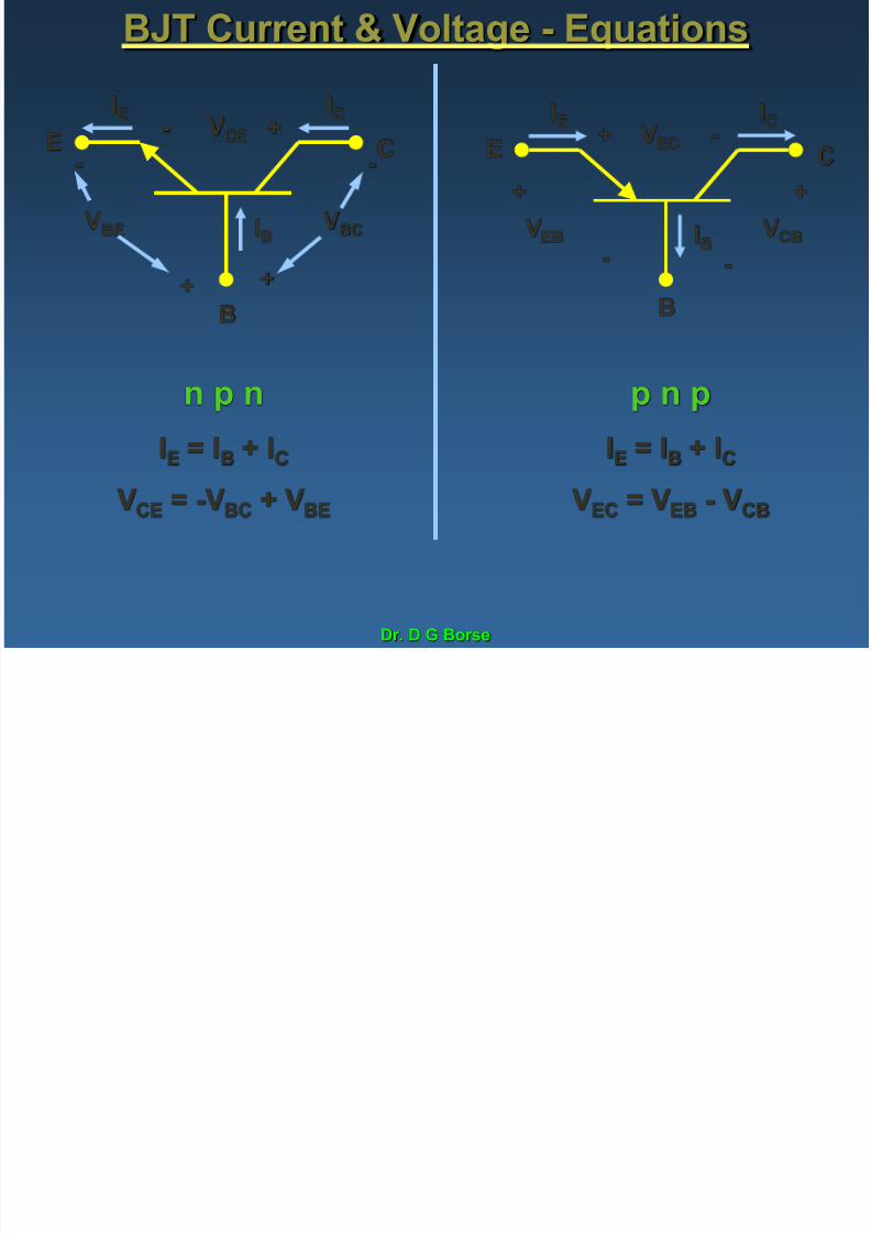
BJT Current & Voltage - Equations
B
CE
IE IC
IB
-
+
VBE VBC
+
-
+- VCE
B
CE
IE IC
IB-
+
VEB VCB
+
-
+ -VEC
n p n
IE = IB + IC
VCE = -VBC + VBE
p n p
IE = IB + IC
VEC = VEB - VCB

7/27/2019 Bjt Basics 1
http://slidepdf.com/reader/full/bjt-basics-1 4/69
Dr. D G Borse
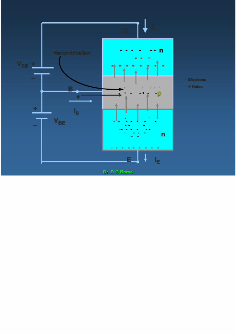
Figure : Current flow (components) for an n-p-n BJT in the active region.
NOTE: Most of the current is due to electrons moving from the emitter through base to the
collector. Base current consists of holes crossing from the base into the emitter and of holes
that recombine with electrons in the base.
- Electrons
+ Holes
VBE
VCB
+
-
+
-
n+
n
p-
IneIpe
-I co
Bulk-recombination
Current
Inc
7/27/2019 Bjt Basics 1
http://slidepdf.com/reader/full/bjt-basics-1 5/69
Dr. D G Borse
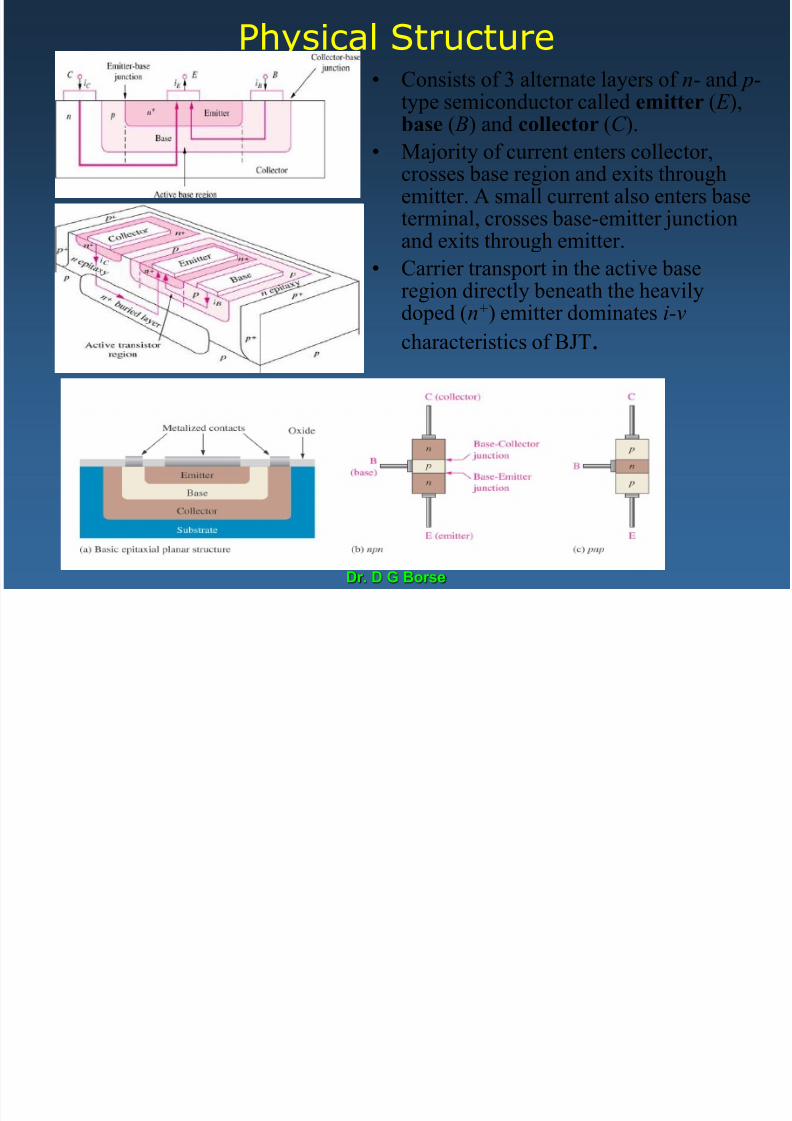
Physical Structure• Consists of 3 alternate layers of n- and p-
type semiconductor called emitter ( E ),base ( B) and collector (C ).
• Majority of current enters collector,crosses base region and exits throughemitter. A small current also enters baseterminal, crosses base-emitter junctionand exits through emitter.
• Carrier transport in the active baseregion directly beneath the heavilydoped (n+) emitter dominates i-v
characteristics of BJT.
7/27/2019 Bjt Basics 1
http://slidepdf.com/reader/full/bjt-basics-1 6/69
Dr. D G Borse
- - - - - -
- - -
- - - - - - - -
- - - - - - -- - --- - - - - -
- - - -- -
- - - - - - - - -
- -
- - - - -
- + - - + - -
Recombination
- Electrons
+ Holes
+
_
+
_
C
B
E
n
p
n
+
IB
Ic
IE
VBE
VCB
7/27/2019 Bjt Basics 1
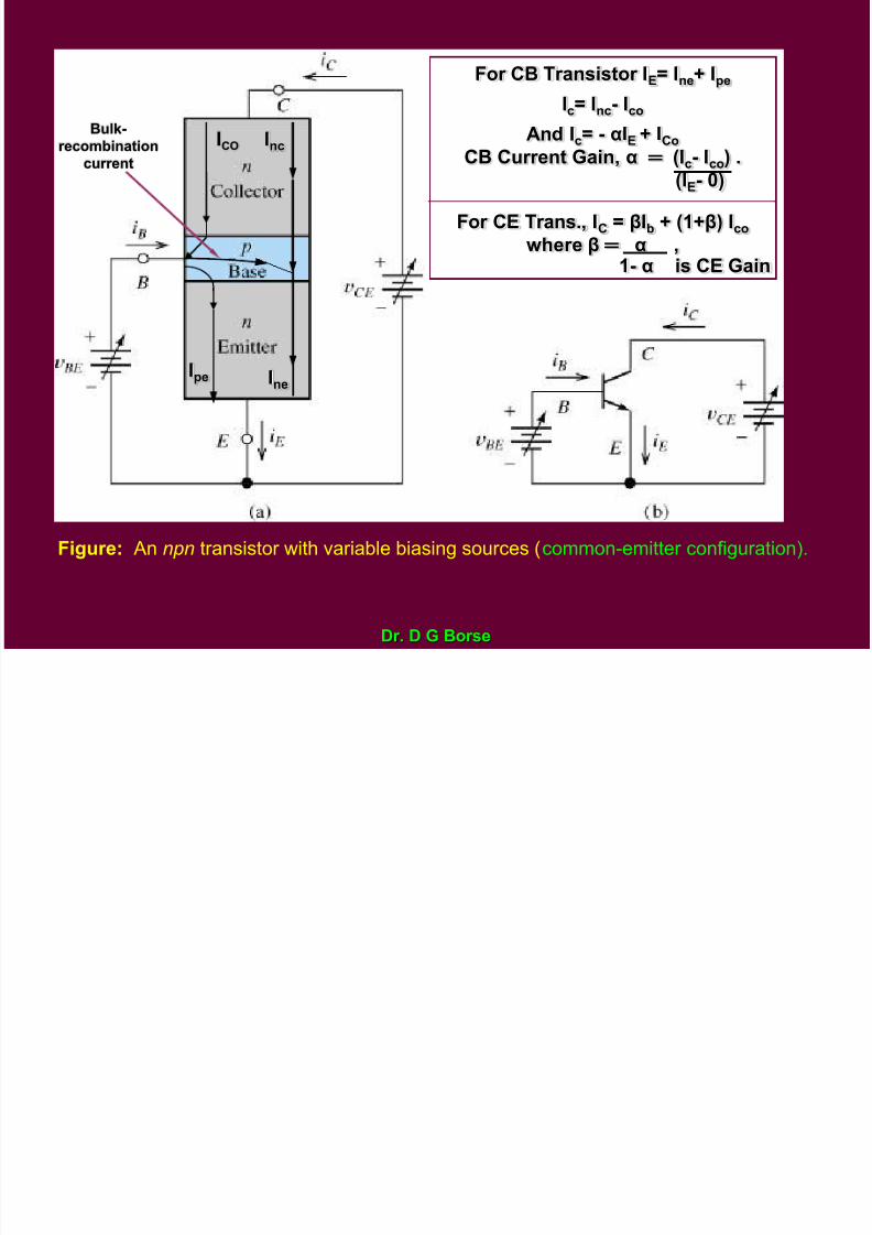
http://slidepdf.com/reader/full/bjt-basics-1 7/69Dr. D G Borse
Figure: An npn transistor with variable biasing sources (common-emitter configuration).
Inc
IneIpe
For CB Transistor IE= Ine+ Ipe
Ic= Inc- Ico
And Ic= - αIE + ICo
CB Current Gain, α ═ (Ic- Ico) .(IE- 0)
For CE Trans., IC = βIb + (1+β) Ico
where β ═ α ,1- α is CE Gain
ICO
Bulk-
recombinationcurrent

7/27/2019 Bjt Basics 1
http://slidepdf.com/reader/full/bjt-basics-1 8/69Dr. D G Borse
Common-Emitter Circuit Diagram
+ _ VC
C
ICVCE
IB
Collector-Current Curves
VCE
IC
Active
Region
IB
Saturation Region
Cutoff Region
IB = 0
Region of
Operation
Description
Active Small base current
controls a large
collector current
Saturation VCE(sat) ~ 0.2V, VCE increases with IC
Cutoff Achieved by reducing IB
to 0, Ideally, IC will also
be equal to 0.

7/27/2019 Bjt Basics 1
http://slidepdf.com/reader/full/bjt-basics-1 9/69Dr. D G Borse
BJT’s have three regions of operation:
1) Active - BJT acts like an amplifier (most common use)
2) Saturation - BJT acts like a short circuit
3) Cutoff - BJT acts like an open circuitBJT is used as a switch by switching
between these two regions.
r sat
Vo
_ +
C
B
E
Saturation Region Model
Vo
_ +
C
B
E
Active Region Model #1
bdc IB
IB
R o
Vo
_ +
C
B
E
Active Region Model #2
bdc IB ICEO
R BB
VCE (V)
IC(mA)
IB = 50 mA
IB = 0
30
5 10 15 200
0
IB = 100 mA
IB = 150 mA
IB = 200 mA
22.5
15
7.5
Saturation Region
Active Region
Cutoff Region
C
E
B
When analyzing a DC
BJT circuit, the BJT
is replaced by one of
the DC circuit models
shown below.
DC Models for a BJT:
7/27/2019 Bjt Basics 1
http://slidepdf.com/reader/full/bjt-basics-1 10/69Dr. D G Borse
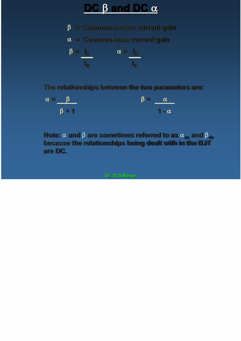
DC b and DC
b = Common-emitter current gain
= Common-base current gainb = IC = IC
IB IE
The relationships between the two parameters are:
= b b =
b + 1 1 -
Note: and b are sometimes referred to as dc and bdc
because the relationships being dealt with in the BJT
are DC.

7/27/2019 Bjt Basics 1
http://slidepdf.com/reader/full/bjt-basics-1 11/69Dr. D G Borse
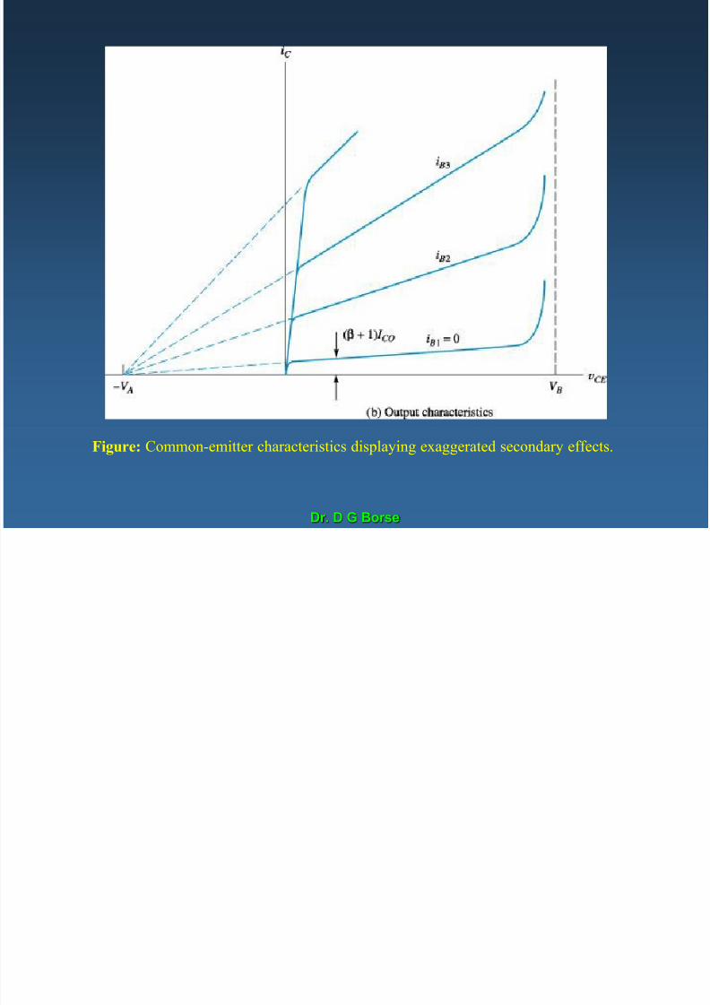
Output characteristics: npn BJT (typical)
VCE (V)
IC(mA)
IB = 50 mA
IB = 0
30
5 10 15 200
0
IB = 100 mA
IB = 150 mA
IB = 200 mA
22.5
15
7.5
Cdc FE
B
I= = h
I b
Note: Two key specifications for the BJT are
Bdc and Vo (or assume Vo is about 0.7 V)
Note: The PE review text
sometimes uses dc instead of bdc.
They are related as follows:
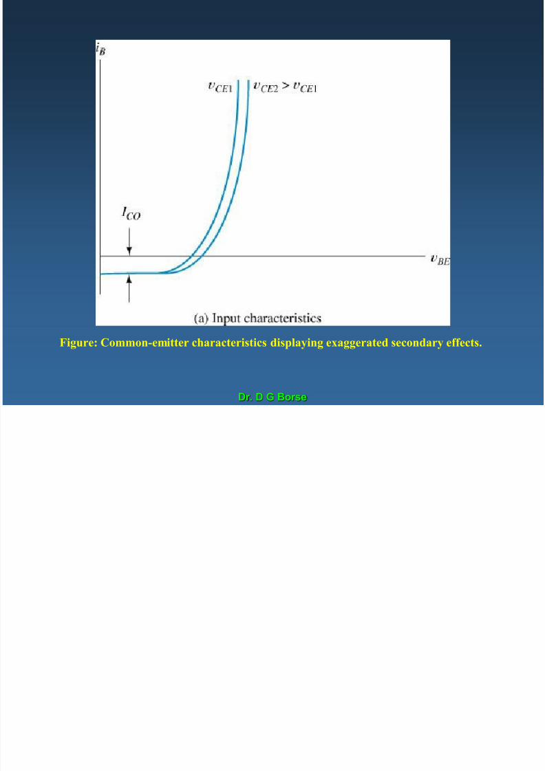
Input characteristics: npn BJT (typical)
VBE (V)
IB(mA)
200
0.5 1.00
0
VCE = 0
150
100
50
VCE = 0.5 V
VCE
> 1 V
The input characteristics look like the characteristics of a
forward-biased diode. Note that VBE varies only slightly,
so we often ignore these characteristics and assume:Common approximation: VBE = Vo = 0.65 to 0.7V
dcdc
dc
=+ 1
b
b
• Find the approximate values
of bdc and dc from the graph.
dc
dc
-1
b dc
7/27/2019 Bjt Basics 1
http://slidepdf.com/reader/full/bjt-basics-1 12/69Dr. D G Borse
Figure: Common-emitter characteristics displaying exaggerated secondary effects.
7/27/2019 Bjt Basics 1
http://slidepdf.com/reader/full/bjt-basics-1 13/69Dr. D G Borse
Figure: Common-emitter characteristics displaying exaggerated secondary effects.
7/27/2019 Bjt Basics 1
http://slidepdf.com/reader/full/bjt-basics-1 14/69Dr. D G Borse
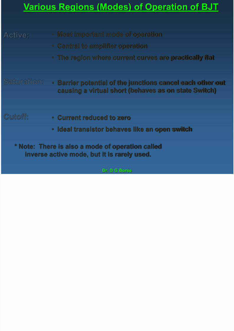
Various Regions (Modes) of Operation of BJT
• Most important mode of operation
• Central to amplifier operation
• The region where current curves are practically flat
Active:
Saturation: • Barrier potential of the junctions cancel each other outcausing a virtual short (behaves as on state Switch)
Cutoff: • Current reduced to zero
• Ideal transistor behaves like an open switch
* Note: There is also a mode of operation called
inverse active mode, but it is rarely used.

7/27/2019 Bjt Basics 1
http://slidepdf.com/reader/full/bjt-basics-1 15/69Dr. D G Borse
BJT Trans-conductance CurveFor Typical NPN Transistor 1
VBE
IC
2 mA
4 mA
6 mA
8 mA
0.7 V
Collector Current:
IC = IES eVBE /VT
Transconductance:
(slope of the curve)
gm = IC / VBE
IES = The reverse saturation current
of the B-E Junction.
VT
= kT/q = 26 mV (@ T=300oK)
= the emission coefficient and is
usually ~1
7/27/2019 Bjt Basics 1
http://slidepdf.com/reader/full/bjt-basics-1 16/69Dr. D G Borse
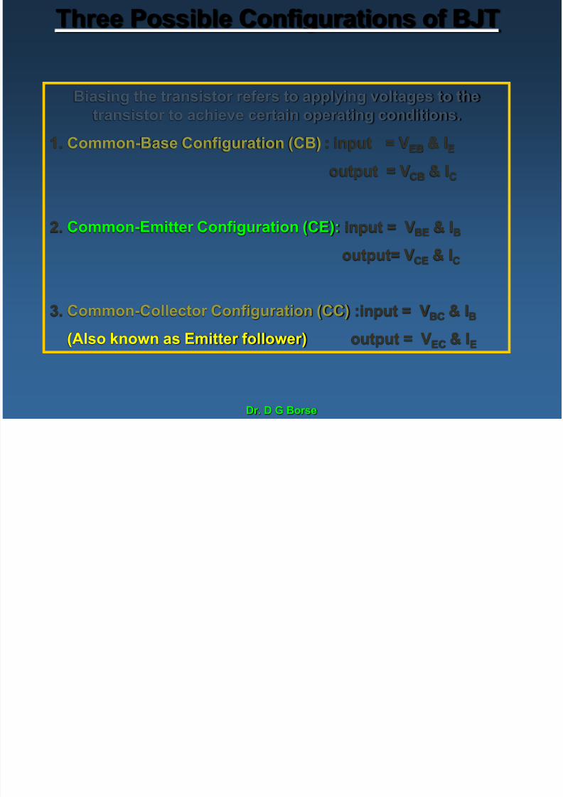
Three Possible Configurations of BJT
Biasing the transistor refers to applying voltages to thetransistor to achieve certain operating conditions.
1. Common-Base Configuration (CB) : input = VEB & IE
output = VCB & IC
2. Common-Emitter Configuration (CE): input = VBE & IB
output= VCE & IC
3. Common-Collector Configuration (CC) :input = VBC & IB
(Also known as Emitter follower) output = VEC & IE

7/27/2019 Bjt Basics 1
http://slidepdf.com/reader/full/bjt-basics-1 17/69Dr. D G Borse
Common-Base BJT Configuration
Circuit Diagram: NPN Transistor
+_ +_
IC IE
IB
VCB VBE
E C
B
VCE
VBEVCB
Region of
OperationIC VCE VBE VCB
C-B
Bias
E-B
Bias
Active bIB
=VBE
+VCE
~0.7V 0V Rev. Fwd.
Saturation Max ~0V ~0.7V -0.7V<VCE<0 Fwd. Fwd.
Cutoff ~0 =VBE+VCE 0V 0V Rev.None
/Rev.
The Table Below lists assumptions
that can be made for the attributes
of the common-base BJT circuit in
the different regions of operation.
Given for a Silicon NPN transistor .
7/27/2019 Bjt Basics 1
http://slidepdf.com/reader/full/bjt-basics-1 18/69Dr. D G Borse
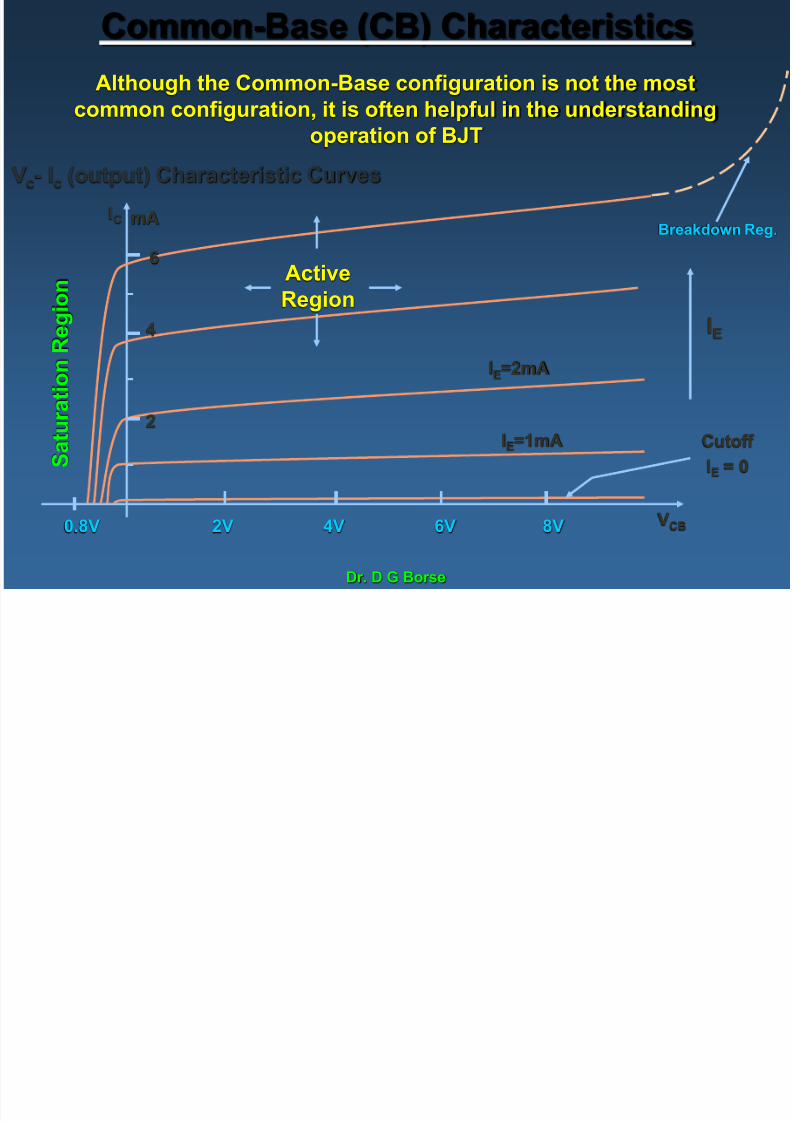
Common-Base (CB) Characteristics
Although the Common-Base configuration is not the most
common configuration, it is often helpful in the understanding
operation of BJTVc- Ic (output) Characteristic Curves
S a t u r
a t i o n R e g i o n
IE
IC
VCB
ActiveRegion
Cutoff
IE = 0
0.8V 2V 4V 6V 8V
mA
2
4
6
IE=1mA
IE=2mA
Breakdown Reg.
C C ll BJT Ch i i
7/27/2019 Bjt Basics 1
http://slidepdf.com/reader/full/bjt-basics-1 19/69Dr. D G Borse
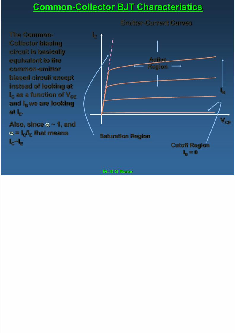
Common-Collector BJT Characteristics
Emitter-Current Curves
VCE
IE
Active
Region
IB
Saturation Region
Cutoff Region
IB = 0
The Common-
Collector biasingcircuit is basically
equivalent to the
common-emitter
biased circuit except
instead of looking at
IC as a function of VCE
and IB we are looking
at IE.
Also, since ~ 1, and = IC /IE that means
IC~IE

7/27/2019 Bjt Basics 1
http://slidepdf.com/reader/full/bjt-basics-1 20/69Dr. D G Borse
n p n Transistor: Forward Active Mode Currents
Forward Collector current is
I co is reverse saturation current
1exp T V BE V
co I C I
A910A1810 co I
V T = kT/q =25 mV at room temperature
Base current is given by
1expco
T V BE V
F F
C I
B I I
b b
50020 F
b
Emitter current is given by
1exp
T V BE V
F
co I
B I
C I
E I
0.1
1
95.0
F
F
F b
b
is forward common-emitter
current gain
is forward common-
base current gain
In this forward active operation region,
F B I
C I
b F
E I
C I
VBE
IE=
IC=
IB=

7/27/2019 Bjt Basics 1
http://slidepdf.com/reader/full/bjt-basics-1 21/69Dr. D G Borse
Various Biasing Circuits used for BJT
• Fixed Bias Circuit
• Collector to Base Bias Circuit
• Potential Divider Bias Circuit

7/27/2019 Bjt Basics 1
http://slidepdf.com/reader/full/bjt-basics-1 22/69
Dr. D G Borse
The Thermal Stability of Operating Point SIco
The Thermal Stability Factor : SIco
SIco = ∂Ic
∂Ico
This equation signifies that Ic Changes SIco times as fast as Ico
Differentiating the equation of Collector Current IC & rearrangingthe terms we can write
SIco ═ 1+β
1- β (∂Ib /∂IC)
It may be noted that Lower is the value of SIco better is the stability
Vbe, β
7/27/2019 Bjt Basics 1
http://slidepdf.com/reader/full/bjt-basics-1 23/69
Dr. D G Borse
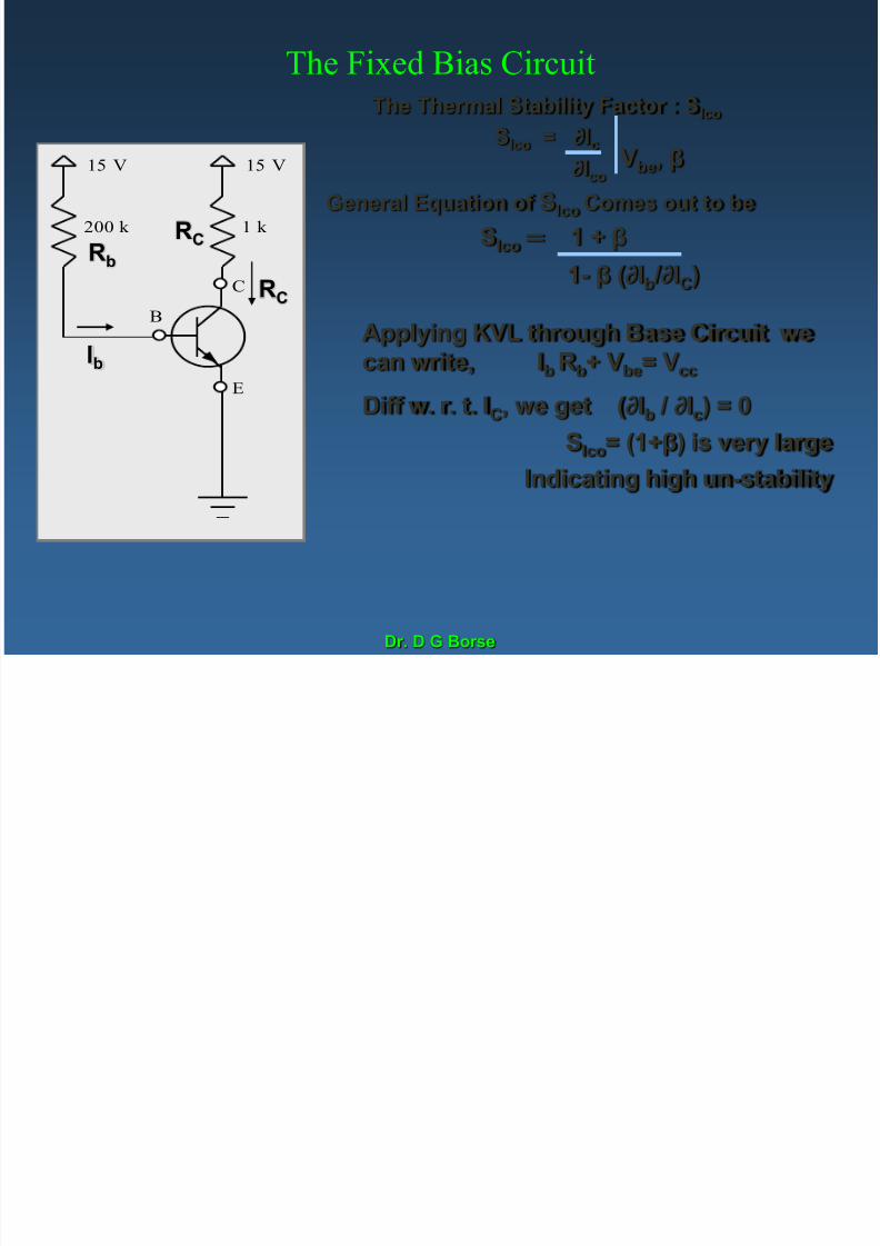
The Fixed Bias Circuit
15 V
C
E
B
15 V
200 k 1 k
The Thermal Stability Factor : SIco
SIco = ∂Ic
∂Ico
General Equation of SIco Comes out to be
SIco ═ 1 + β
1- β (∂Ib /∂IC)
Vbe, β
Applying KVL through Base Circuit we
can write, Ib Rb+ Vbe= Vcc
Diff w. r. t. IC, we get (∂Ib / ∂Ic) = 0
SIco= (1+β) is very large
Indicating high un-stability
Ib
Rb
RC
RC
7/27/2019 Bjt Basics 1
http://slidepdf.com/reader/full/bjt-basics-1 24/69
Dr. D G Borse
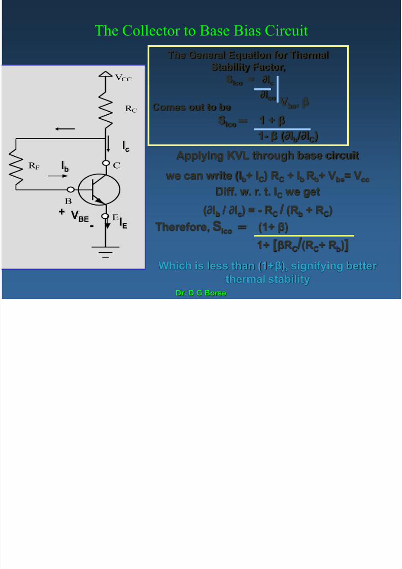
The Collector to Base Bias Circuit
The General Equation for Thermal
Stability Factor,SIco = ∂Ic
∂Ico
Comes out to be
SIco ═ 1 + β
1- β (∂Ib /∂I
C)
Vbe, β
Applying KVL through base circuit
we can write (Ib+ IC) RC + Ib Rb+ Vbe= Vcc
Diff. w. r. t. IC we get
(∂Ib / ∂Ic) = - RC / (Rb + RC)Therefore, SIco ═ (1+ β)
1+ [βRC /(RC+ Rb)]
Which is less than (1+β), signifying better
thermal stability
VCC
R C
C
E
B
R F
Ic
Ib
VBE+- IE
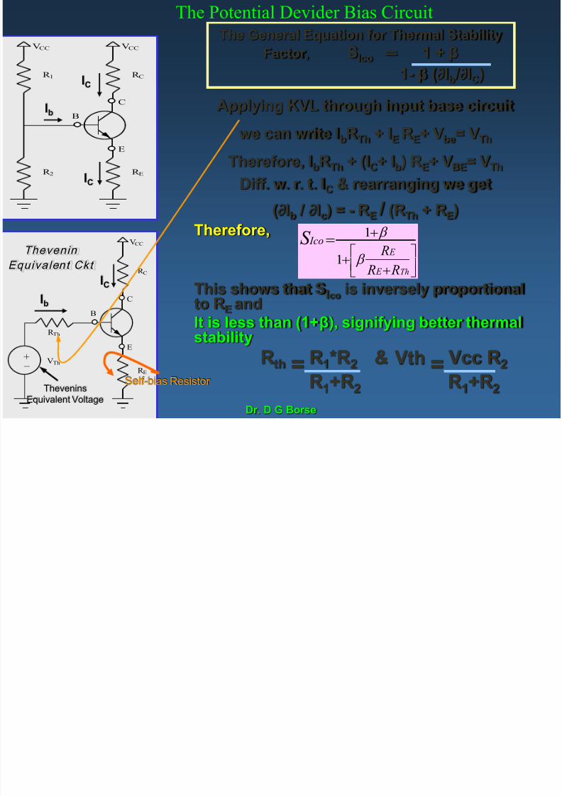
The Potential Devider Bias Circuit
7/27/2019 Bjt Basics 1
http://slidepdf.com/reader/full/bjt-basics-1 25/69
Dr. D G Borse
The Potential Devider Bias Circuit
VCC
R C
C
E
B
VCC
R 1
R ER 2
The General Equation for Thermal Stability
Factor, SIco ═ 1 + β
1- β (∂Ib /∂IC)
Applying KVL through input base circuit
we can write IbRTh + IE RE+ Vbe= VTh
Therefore, IbRTh + (IC+ Ib) RE+ VBE= VTh
Diff. w. r. t. IC & rearranging we get
(∂Ib / ∂Ic) = - RE / (RTh + RE)
Therefore,
This shows that SIco is inversely proportionalto RE and
It is less than (1+β), signifying better thermalstability
VCC
R C
C
E
B
R E
R Th
VTh _ +
Thevenin
Equivalent Ckt
IC
Ib
IC
Ib
IC
Thevenins
Equivalent Voltage
Self-bias Resistor
Rth = R1*R2 & Vth = Vcc R2
R1
+R2
R1
+R2
Th R R
R
E
E
IcoS b
b
1
1
7/27/2019 Bjt Basics 1
http://slidepdf.com/reader/full/bjt-basics-1 26/69
Dr. D G Borse
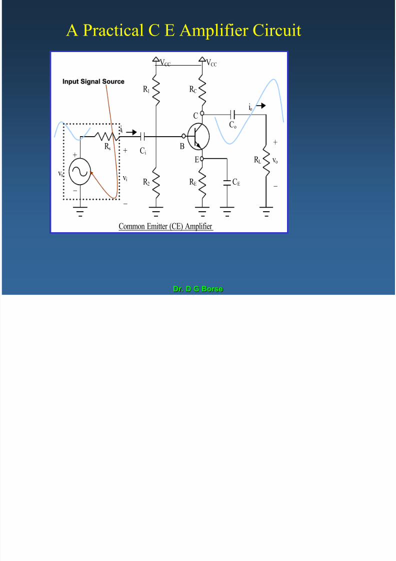
A Practical C E Amplifier Circuit
VCC
R C
C
E
B
VCC
R 1
R ER 2
R s Ci
R L
Co
CEvi
vo
+
+
vs
+
_ _
_
io
ii
Common Emitter (CE) Amplifier
Input Signal Source
7/27/2019 Bjt Basics 1
http://slidepdf.com/reader/full/bjt-basics-1 27/69
Dr. D G Borse
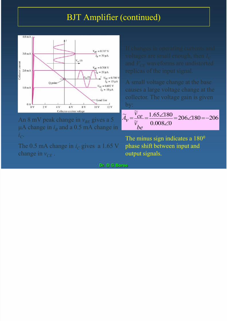
BJT Amplifier (continued)
An 8 mV peak change in v BE gives a 5mA change in i B and a 0.5 mA change in
iC .
The 0.5 mA change in iC gives a 1.65 V
change in vCE .
If changes in operating currents and
voltages are small enough, then I C
and V CE waveforms are undistorted
replicas of the input signal.
A small voltage change at the basecauses a large voltage change at the
collector. The voltage gain is given
by:
The minus sign indicates a 1800
phase shift between input and
output signals.
2061802060008.0
18065.1
~
~~
be
v
cev
v A

7/27/2019 Bjt Basics 1
http://slidepdf.com/reader/full/bjt-basics-1 28/69
Dr. D G Borse
A Practical BJT Amplifier using Coupling and Bypass
Capacitors
• AC coupling through capacitors is used to inject an ac input signal
and extract the ac output signal without disturbing the DC Q-point
• Capacitors provide negligible impedance at frequencies of interest
and provide open circuits at dc.
In a practical amplifier design, C 1 and C 3 are
large coupling capacitors or dc blockingcapacitors, their reactance (XC = |ZC| = 1/wC ) at
signal frequency is negligible. They are effective
open circuits for the circuit when DC bias isconsidered.
C 2 is a bypass capacitor. It provides a low
impedance path for ac current from emitter to
ground. It effectively removes RE (required for good Q-point stability) from the circuit when ac
signals are considered.

7/27/2019 Bjt Basics 1
http://slidepdf.com/reader/full/bjt-basics-1 29/69
Dr. D G Borse
D C Equivalent for the BJT Amplifier (Step1)
• All capacitors in the original amplifier circuit are replaced by opencircuits, disconnecting v I , R I , and R3 from the circuit and leaving R E
intact. The the transistor Q will be replaced by its DC model.
DC Equivalent Circuit
7/27/2019 Bjt Basics 1
http://slidepdf.com/reader/full/bjt-basics-1 30/69
Dr. D G Borse
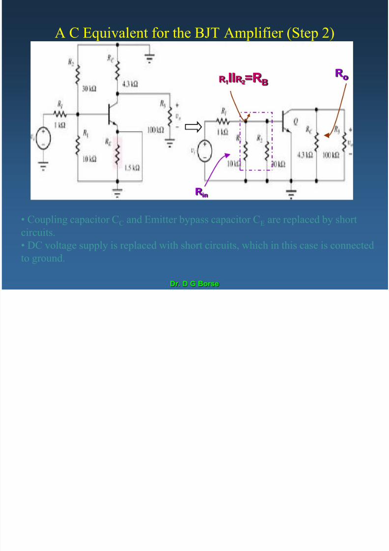
A C Equivalent for the BJT Amplifier (Step 2)
• Coupling capacitor CC and Emitter bypass capacitor CE are replaced by short
circuits.
• DC voltage supply is replaced with short circuits, which in this case is connected
to ground.
R1IIR2=RB
Rin
Ro

7/27/2019 Bjt Basics 1
http://slidepdf.com/reader/full/bjt-basics-1 31/69
Dr. D G Borse
A C Equivalent for the BJT Amplifier(continued)
100k Ω4.3k Ω3R CR R
30k Ω10k Ω2
R 1
R B
R
• By combining parallel resistors into equivalent R B and R, the equivalent AC
circuit above is constructed. Here, the transistor will be replaced by itsequivalent small-signal AC model (to be developed).
All externally connected capacitors are assumedas short circuited elements for ac signal
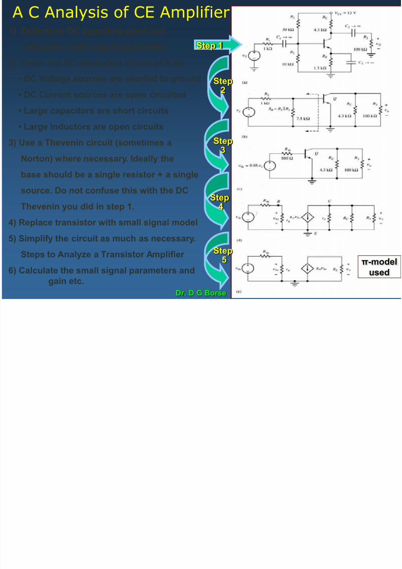
A C Analysis of CE Amplifier
7/27/2019 Bjt Basics 1
http://slidepdf.com/reader/full/bjt-basics-1 32/69
Dr. D G Borse
A C Analysis of CE Amplifier1) Determine DC operating point and
calculate small signal parameters
2) Draw the AC equivalent circuit of Amp.
• DC Voltage sources are shorted to ground
• DC Current sources are open circuited
• Large capacitors are short circuits
• Large inductors are open circuits
3) Use a Thevenin circuit (sometimes a
Norton) where necessary. Ideally the
base should be a single resistor + a single
source. Do not confuse this with the DC
Thevenin you did in step 1.
4) Replace transistor with small signal model
5) Simplify the circuit as much as necessary.
Steps to Analyze a Transistor Amplifier
6) Calculate the small signal parameters and
gain etc.
Step 1
Step2
Step3
Step4
Step5 π-model
used
7/27/2019 Bjt Basics 1
http://slidepdf.com/reader/full/bjt-basics-1 33/69
Dr. D G Borse
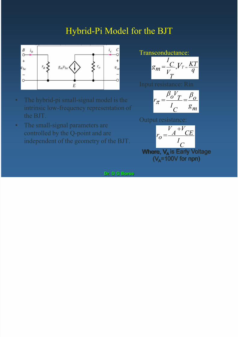
Hybrid-Pi Model for the BJT
• The hybrid-pi small-signal model is the
intrinsic low-frequency representation of
the BJT.
• The small-signal parameters arecontrolled by the Q-point and are
independent of the geometry of the BJT.
Transconductance:
q KT
T V
C I
m g T V ,
Input resistance: Rin
m g
o
C I
T V o
r b b
Output resistance:
C I
CE V
AV
or
Where, V A is Early Voltage
(V A=100V for npn)

7/27/2019 Bjt Basics 1
http://slidepdf.com/reader/full/bjt-basics-1 34/69
Dr. D G Borse
Hybrid Parameter Model
hi
hr V
oh
oh
f I
iV
i
I i
2
2'
I o
V o
1
1'
11 12
21 22
i i o i i r o
o i o f i o o
V h I h V h I h V
I h I h V h I h V
Linear Twoport DeviceVi
Ii Io
Vo

7/27/2019 Bjt Basics 1
http://slidepdf.com/reader/full/bjt-basics-1 35/69
Dr. D G Borse
11 12
21 22
0 0
0 0
i i
o ii o
o o
o ii o
V V h hV I I V
I I
h hV I I V
h -Parameters
h11 = hi = Input Resistance
h12 = hr = Reverse Transfer Voltage Ratioh21 = h f = Forward Transfer Current Ratioh22 = ho = Output Admittance
Th S ll i l M d l f CE T i t
7/27/2019 Bjt Basics 1
http://slidepdf.com/reader/full/bjt-basics-1 36/69
Dr. D G Borse
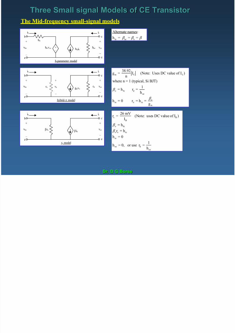
The Mid-frequency small-signal models
b
e
hoe
hie
hrevce hfei b v be
i b ic
vce
c
e
+ _
+ +
_ _
h-parameter model
b
e
r dgmv v be
i b ic
vce
c
e
+ +
_ _
hybrid- model
r v
+
_
b
e
bi b v be
i b ic
vce
c
e
+ +
_ _
r e model
br e
fe ac o
Alternate names:
h = = = b b b
m C C
o fe d
oe
ore ie
m
38.92g = I (Note: Uses DC value of I )
n
where n = 1 (typical, Si BJT)
1= h r =
h
h = 0 r = h =g
b
b
e B
B
o fe
o e ie
re
oe d
oe
26 mVr = (Note: uses DC value of I )
I
= h
r = h
h = 0
1h = 0, or use r =
h
b b
Three Small signal Models of CE Transistor
BJT Mid f A l i i th h b id d l

7/27/2019 Bjt Basics 1
http://slidepdf.com/reader/full/bjt-basics-1 37/69
Dr. D G Borse
BJT Mid-frequency Analysis using the hybrid- model:
b
e
r dgmv vi
ii
io
vo
c
e
+ +
_ _
mid-frequency CE amplifier circuit
r v
+
_
R C R LR Thvs
+
_
is
R S
A common emitter (CE) amplifier VCC
R C
C
E
B
VCC
R 1
R ER 2
R s Ci
R L
Co
CEvi
vo
+
+
vs
+
_ _
_
io
ii
The mid-frequency circuit is drawn as follows:
• the coupling capacitors (Ci and Co) and thebypass capacitor (CE) are short circuits
• short the DC supply voltage (superposition)
• replace the BJT with the hybrid- model
The resulting mid-frequency circuit is shown belo
si
iv
s
i
i
o
s
o
svC Lo L Lmi
ov R Z
Z A
v
v
v
v
v
v A R Rr R R g
v
v A where, , ,''
Rwhere,21
R Rr R I
v Z
ThTh
i
i
i ,
C o
ovo
o
o Rr
i
v
Z
i
i
o
i i
i A
An a c Equivalent Circuitr o
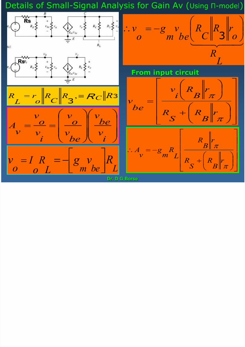
Details of Small-Signal Analysis for Gain Av (Using Π-model)
7/27/2019 Bjt Basics 1
http://slidepdf.com/reader/full/bjt-basics-1 38/69
Dr. D G Borse
Details of Small Signal Analysis for Gain Av (Using Π model)
3
3 RC R
C R
or
L R R ,
iv
bev
bev
ov
iv
ov
v A
Lbem
Rv g v
L
R
o
I
o
Rs
Rs
L R
or R
C R
bev
m g
ov
3
r B
RS
R
r B
R
L R
m g
v A
r B
RS
R
r B
Riv
bev
From input circuit

7/27/2019 Bjt Basics 1
http://slidepdf.com/reader/full/bjt-basics-1 39/69
Dr. D G Borse
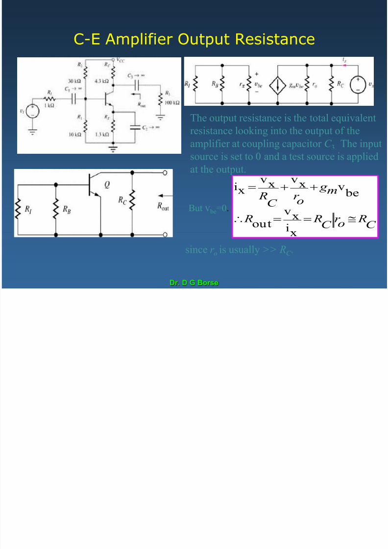
C-E Amplifier Input Resistance
• The input resistance, the total resistance
looking into the amplifier at couplingcapacitor C 1, represents the total
resistance presented to the AC source.
r R Rr B
R R
r
B
R
21xixv
in
)(xixv
7/27/2019 Bjt Basics 1
http://slidepdf.com/reader/full/bjt-basics-1 40/69

7/27/2019 Bjt Basics 1
http://slidepdf.com/reader/full/bjt-basics-1 41/69
Dr. D G Borse
High-Frequency Response – BJT Amplifiers
Capacitances that will affect the high-frequency response:
• Cbe, Cbc, Cce – internal capacitances
• Cwi, Cwo – wiring capacitances
• CS, CC – coupling capacitors
• CE – bypass capacitor
Frequency Response of Amplifiers

7/27/2019 Bjt Basics 1
http://slidepdf.com/reader/full/bjt-basics-1 42/69
Dr. D G Borse
Frequency Response of Amplifiers
The voltage gain of an amplifier is typically flat over the mid-frequency
range, but drops drastically for low or high frequencies. A typical
frequency response is shown below.
LM(Avi) = 20log(vo/vi) [in dB]
BW
3dB
20log(Avi(mid))
f f LOW f HIGH
LM Response for a General Amplifier
For a CE BJT: (shown on lower right)• low-frequency drop-off is due to CE, Ci and Co • high-frequency drop-off is due to device capacitances Cp and Cm
(combined to form Ctotal)• Each capacitor forms a break point (simple pole or zero) with a break
frequency of the form f=1/(2pR EqC), where R Eq is the resistance seen bythe capacitor
• CE usually yields the highest low-frequency breakwhich establishes f Low.

7/27/2019 Bjt Basics 1
http://slidepdf.com/reader/full/bjt-basics-1 43/69
Dr. D G Borse
Amplifier Power Dissipation
• Static power dissipation in amplifiers is determined from their DCequivalent circuits.
P D
V CE
I C
V BE
I B
Total power dissipated in C-B
and E-B junctions is:
where
Total power supplied is:
B I I I I
C I
CC V
S P
12 where ,
2
BE V CBV CE V
E R
F EQ R
BE V
EQV
B I
R R
CC V
I
1
and
211
b
The difference is the power dissipated by the bias resistors.
7/27/2019 Bjt Basics 1
http://slidepdf.com/reader/full/bjt-basics-1 44/69
Dr. D G Borse
7/27/2019 Bjt Basics 1
http://slidepdf.com/reader/full/bjt-basics-1 45/69
Dr. D G Borse
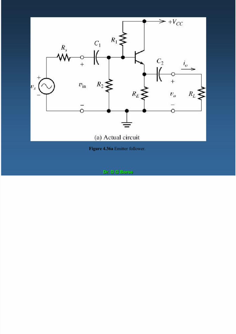
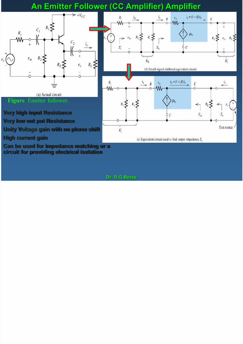
Figure 4.36a Emitter follower.
An Emitter Follower (CC Amplifier) Amplifier
7/27/2019 Bjt Basics 1
http://slidepdf.com/reader/full/bjt-basics-1 46/69
Dr. D G Borse
Figure Emitter follower.
Very high input Resistance
Very low out put Resistance
Unity Voltage gain with no phase shiftHigh current gain
Can be used for impedance matching or acircuit for providing electrical isolation
( p ) p

7/27/2019 Bjt Basics 1
http://slidepdf.com/reader/full/bjt-basics-1 47/69
Dr. D G Borse
Figure 4.36b Emitter follower.

7/27/2019 Bjt Basics 1
http://slidepdf.com/reader/full/bjt-basics-1 48/69
7/27/2019 Bjt Basics 1
http://slidepdf.com/reader/full/bjt-basics-1 49/69
Dr. D G Borse
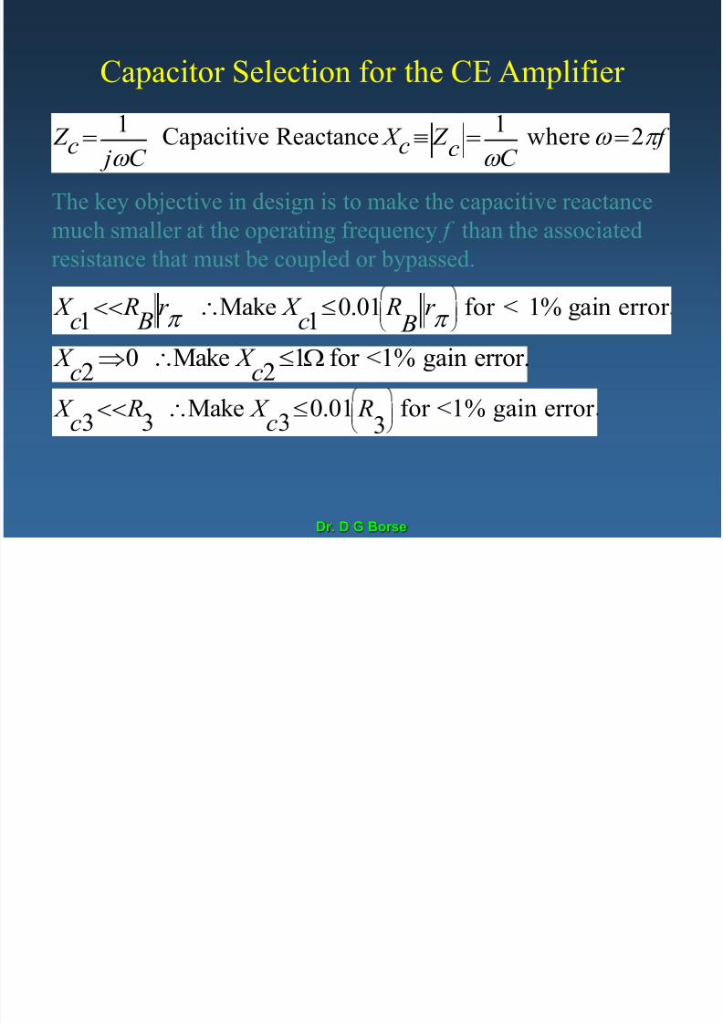
Capacitor Selection for the CE Amplifier
Z c 1 jw C
Capacitive Reactance X c Z c 1w C
where w 2 f
X c1
R Br
Make X c1
0.01 R B
r
for < 1% gain error
X
c2
0 Make X
c2
1 for <1% gain error.
X c3
R3 Make X
c30.01 R
3
for <1% gain error
The key objective in design is to make the capacitive reactance
much smaller at the operating frequency f than the associated
resistance that must be coupled or bypassed.
7/27/2019 Bjt Basics 1
http://slidepdf.com/reader/full/bjt-basics-1 50/69
Dr. D G Borse
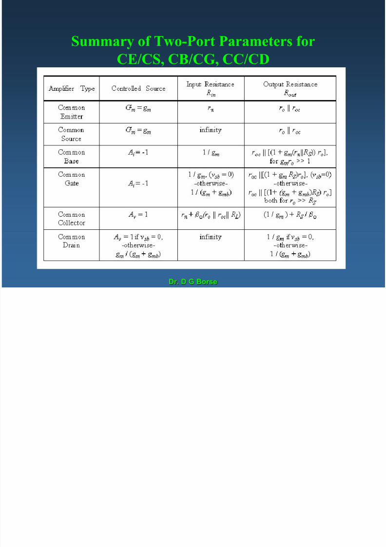
Summary of Two-Port Parameters for
CE/CS, CB/CG, CC/CD
7/27/2019 Bjt Basics 1
http://slidepdf.com/reader/full/bjt-basics-1 51/69
Dr. D G Borse
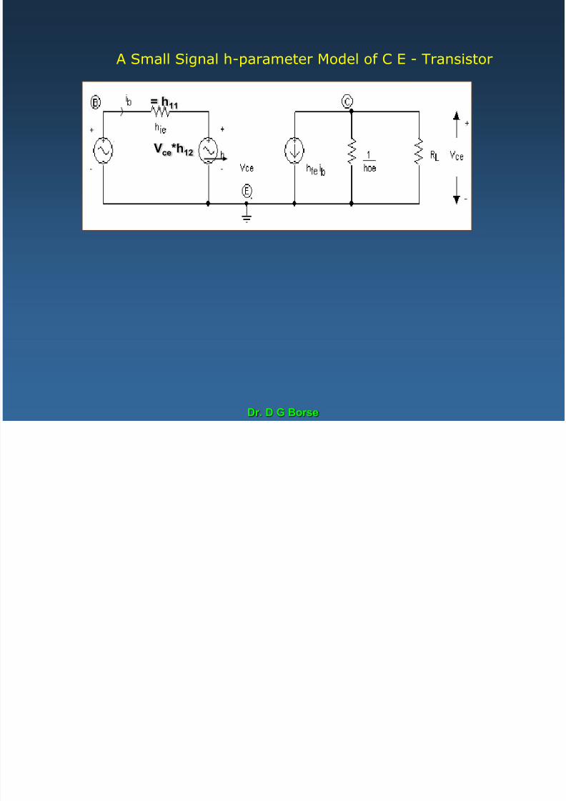
A Small Signal h-parameter Model of C E - Transistor
= h11
Vce*h12

7/27/2019 Bjt Basics 1
http://slidepdf.com/reader/full/bjt-basics-1 52/69
Dr. D G Borse
A Simple MOSFET Amplifier
The MOSFET is biased in the saturation region by dc voltage sources V GS and
V DS = 10 V. The DC Q-point is set at (V DS , I DS ) = (4.8 V, 1.56 mA) with V GS =
3.5 V.
Total gate-source voltage is: gsvGS
V GS
v
A 1 V p-p change in vGS gives a 1.25 mA p-p change in i DS and a 4 V p-p change
in v DS . Notice the characteristic non-linear I/O relationship compared to the BJT.
Eber-Moll BJT Model

7/27/2019 Bjt Basics 1
http://slidepdf.com/reader/full/bjt-basics-1 53/69
Dr. D G Borse
Eber Moll BJT Model
The Eber-Moll Model for BJTs is fairly complex, but it is
valid in all regions of BJT operation. The circuit diagram
below shows all the components of the Eber-Moll Model:
E C
B
IRIF
IE IC
IB
RIERIC
Eber-Moll BJT Model

7/27/2019 Bjt Basics 1
http://slidepdf.com/reader/full/bjt-basics-1 54/69
Dr. D G Borse
be o J ode
R = Common-base current gain (in forward active mode)
F = Common-base current gain (in inverse active mode)IES = Reverse-Saturation Current of B-E Junction
ICS = Reverse-Saturation Current of B-C Junction
IC = FIF – IR IB = IE - IC
IE = IF - RIR
IF = IES [exp(qVBE /kT) – 1] IR = IC [exp (qVBC /kT) – 1]
If IES & ICS are not given, they can be determined using various
BJT parameters.
Small Signal BJT Equivalent Circuit
7/27/2019 Bjt Basics 1
http://slidepdf.com/reader/full/bjt-basics-1 55/69
Dr. D G Borse
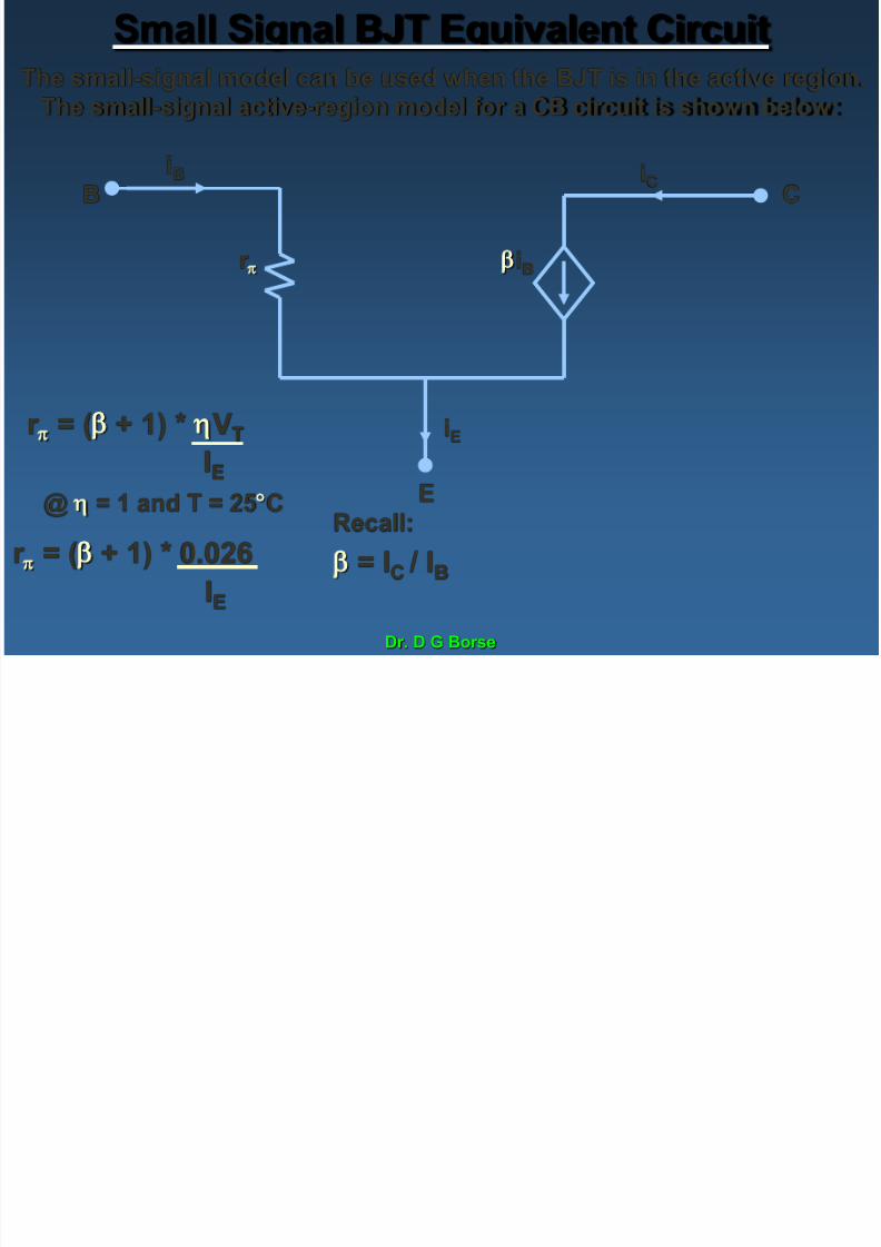
g qThe small-signal model can be used when the BJT is in the active region.
The small-signal active-region model for a CB circuit is shown below:
biBr
iE
iCiBB C
E
r = (b + 1) * VT
IE@ = 1 and T = 25C
r = (b + 1) * 0.026
IE
Recall:
b = IC / IB
The Early Effect (Early Voltage)
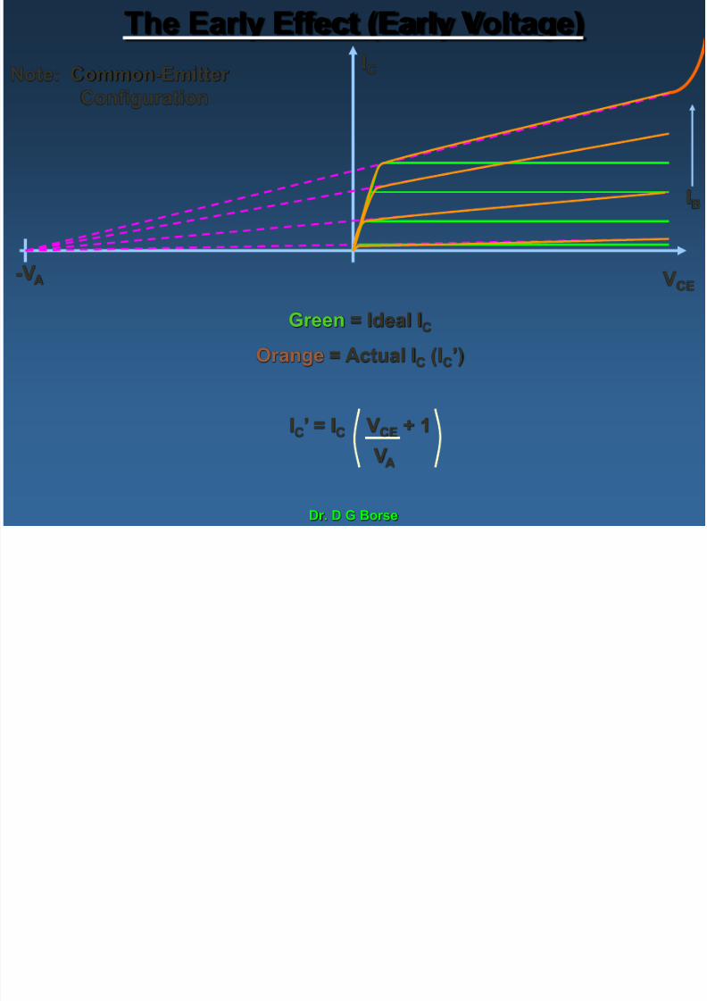
7/27/2019 Bjt Basics 1
http://slidepdf.com/reader/full/bjt-basics-1 56/69
Dr. D G Borse
y ( y g )
VCE
ICNote: Common-Emitter
Configuration
-VA
IB
Green = Ideal IC
Orange = Actual IC (IC’)
IC’ = IC VCE + 1
VA
Early Effect Example

7/27/2019 Bjt Basics 1
http://slidepdf.com/reader/full/bjt-basics-1 57/69
Dr. D G Borse
y p
Given: The common-emitter circuit below with IB = 25mA,
VCC = 15V, b = 100 and VA = 80.
Find: a) The ideal collector current
b) The actual collector current
Circuit Diagram
+ _ VCC
ICVCE
IB
b = 100 = IC /I
B
a)
IC = 100 * IB = 100 * (25x10-6 A)
IC = 2.5 mA
b) IC’ = IC VCE + 1 = 2.5x10⁻³ 15 + 1 = 2.96 mA
VA 80
IC’ = 2.96 mA
Breakdown Voltage
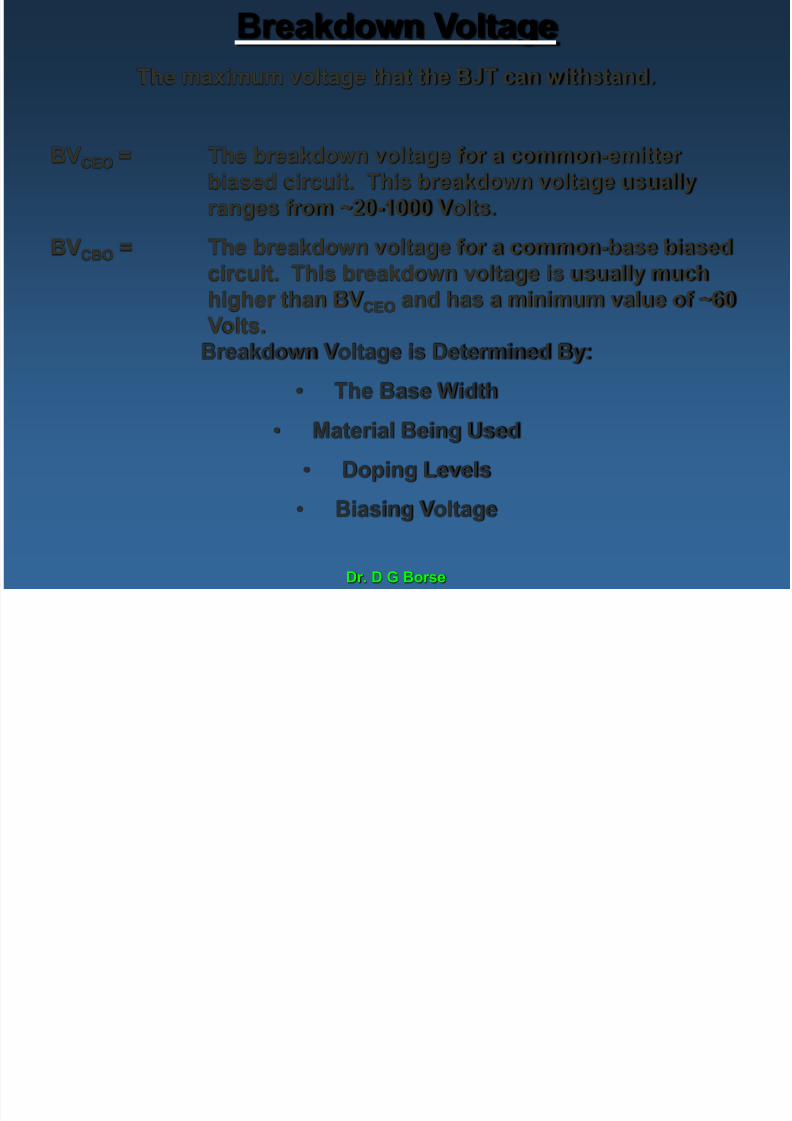
7/27/2019 Bjt Basics 1
http://slidepdf.com/reader/full/bjt-basics-1 58/69
Dr. D G Borse
g
The maximum voltage that the BJT can withstand.
BVCEO = The breakdown voltage for a common-emitter biased circuit. This breakdown voltage usually
ranges from ~20-1000 Volts.
BVCBO = The breakdown voltage for a common-base biased
circuit. This breakdown voltage is usually much
higher than BVCEO and has a minimum value of ~60
Volts.
Breakdown Voltage is Determined By:
• The Base Width
• Material Being Used
• Doping Levels
• Biasing Voltage
7/27/2019 Bjt Basics 1
http://slidepdf.com/reader/full/bjt-basics-1 59/69
Dr. D G Borse
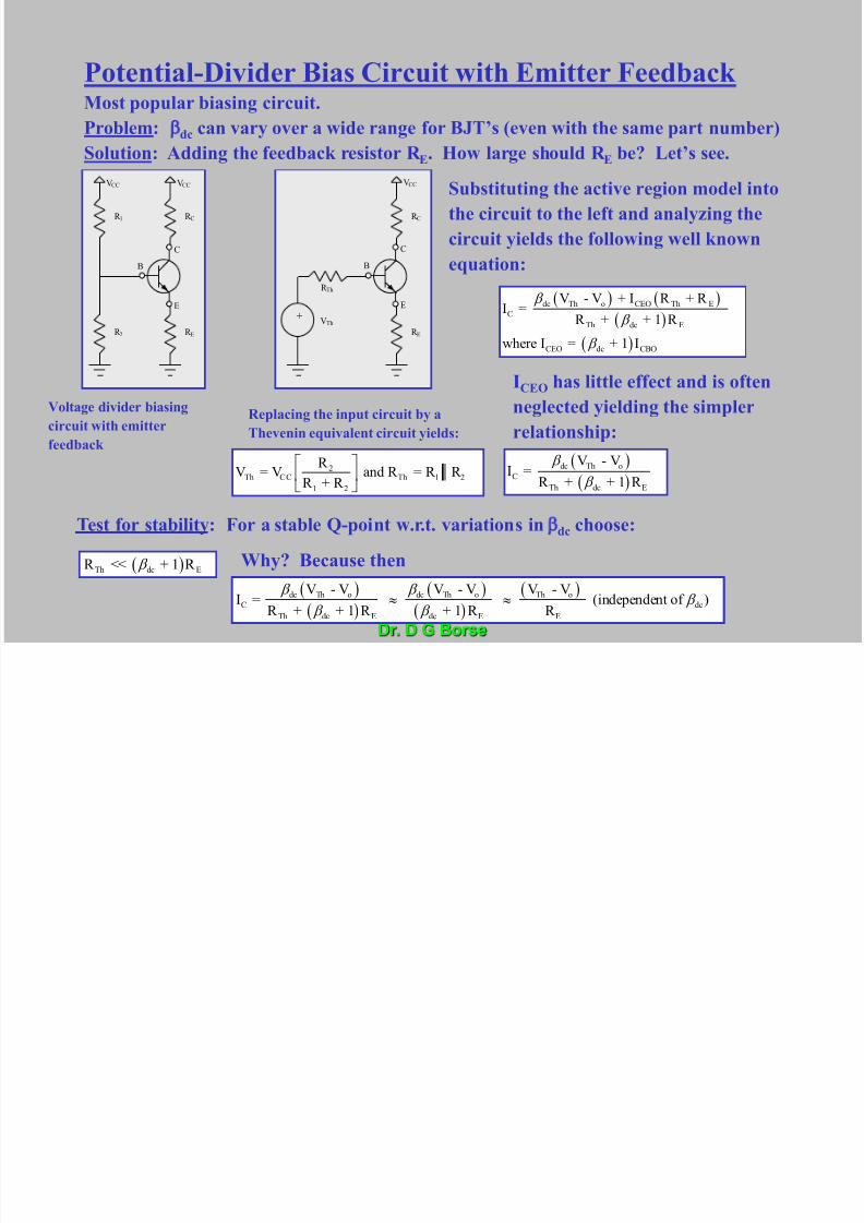
Potential-Divider Bias Circuit with Emitter Feedback Most popular biasing circuit.
Problem: bdc can vary over a wide range for BJT’s (even with the same part number)
Solution: Adding the feedback resistor R E. How large should R E be? Let’s see. Substituting the active region model into
the circuit to the left and analyzing the
circuit yields the following well known
equation:
VCC
R C
C
E
B
VCC
R 1
R ER 2
VCC
R C
C
E
B
R E
R Th
VTh _ +
2Th CC Th 1 2
1 2
R V = V and R = R R R + R
dc Th o CEO Th E
C
Th dc E
CEO dc CBO
V - V + I R + R
I = R + + 1 R
where I = + 1 I
b
b
b
ICEO has little effect and is often
neglected yielding the simpler
relationship:
dc Th o
C
Th dc E
V - VI =R + + 1 R
b b
Test for stability: For a stable Q-point w.r.t. variations in bdc choose:
Th dc ER << + 1 R b Why? Because then
dc Th o dc Th o Th o
C dc
Th dc E dc E E
V - V V - V V - VI = (independent of )
R + + 1 R + 1 R R
b b b
b b
Voltage divider biasing
circuit with emitter
feedback
Replacing the input circuit by a
Thevenin equivalent circuit yields:
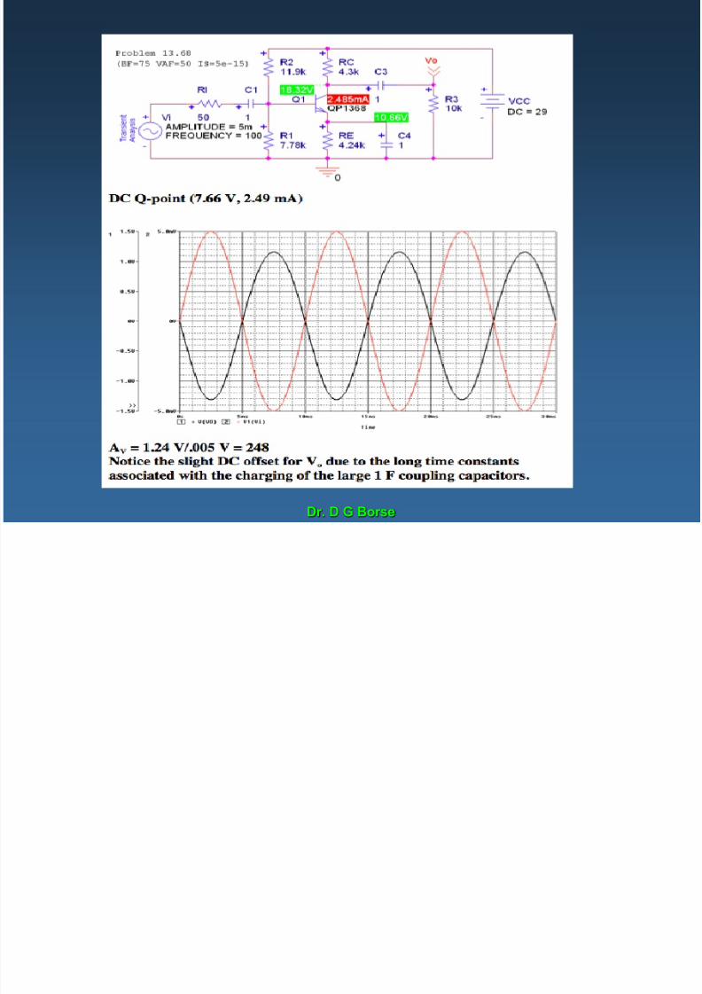
PE-Electrical Review Course - Class 4 (Transistors)
7/27/2019 Bjt Basics 1
http://slidepdf.com/reader/full/bjt-basics-1 60/69
Dr. D G Borse
( )
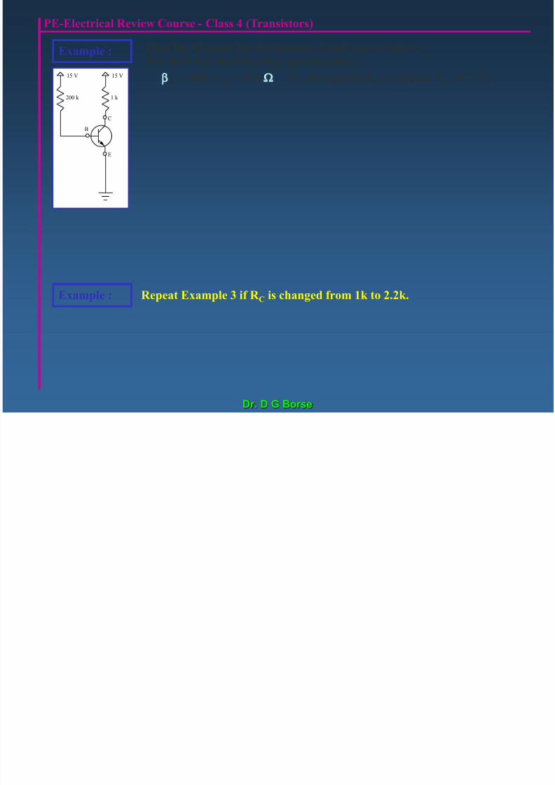
Example : Find the Q-point for the biasing circuit shown below.
The BJT has the following specifications:
bdc = 100, rsat = 100 (Vo not specified, so assume Vo = 0.7 V)15 V
C
E
B
15 V
200 k 1 k
Example : Repeat Example 3 if R C is changed from 1k to 2.2k.
PE-Electrical Review Course - Class 4 (Transistors)

7/27/2019 Bjt Basics 1
http://slidepdf.com/reader/full/bjt-basics-1 61/69
Dr. D G Borse
Example Determine the Q-point for the biasing circuit shown.
The BJT has the following specifications:
bdc varies from 50 to 400, Vo = 0.7 V, ICBO = 10 nA
Solution:
Case 1: bdc = 50C
E
B
18 V
30 k
15 k
10 k
8 k
18 V
Case 2: bdc = 400 Similar to Case 1 above. Results are: IC = 0.659 mA, VCE =
6.14 V Summary:
bdc IC VCE50
400
PE-Electrical Review Course - Class 4 (Transistors)
7/27/2019 Bjt Basics 1
http://slidepdf.com/reader/full/bjt-basics-1 62/69
Dr. D G Borse
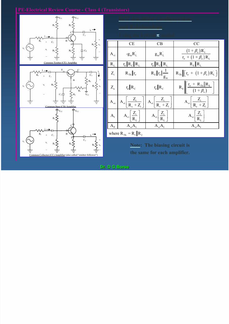
BJT Amplifier Configurations
and Relationships:
Using the hybrid- model.
VCC
R C
C
E
B
VCC
R 1
R ER 2
R sCi
R L
Co
CEvi
vo+
+
vs
+
_ _
_
io
ii
Common Emitter (CE) Amplifier
'
o L' '
vi m L m L '
o L
'
L d C L d C L E L
'
i Th E Th o L
m
Th S
o d C d C E
o
i i ivs vi vi vi
s i s i s i
CE CB CC
1 + R A -g R g R
r + 1 + R
R r R R r R R R R
1Z R r R r R r + 1 + R
g
r + R R Z r R r R R
1 +
Z Z ZA A A A
R + Z R + Z R + Z
b
b
b
b
i i iI vi vi vi
L L L
P vi I vi I vi I
Th 1 2
Z Z ZA A A A
R R R
A A A A A A A
where R = R R
VCC
R C
E
R 2
R E
R s Ci
R L
Co
C2
vi vo
+
+
vs
+
_ _ _
ioii
Common Base (CB) Amplifier
R 1
C
B
VCC
C
E
B
VCC
R 1
R ER 2
R s Ci
vi
+
vs
+
_
_
R L
Co
vo
+
_
io
ii
Common Collector (CC) Amplifier (also called “emitter -follower”)
Note: The biasing circuit is
the same for each amplifier.
7/27/2019 Bjt Basics 1
http://slidepdf.com/reader/full/bjt-basics-1 63/69
Dr. D G Borse
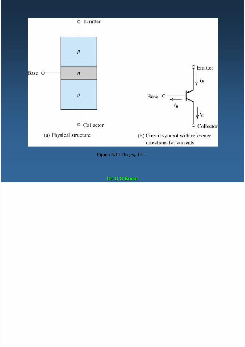
Figure 4.16 The pnp BJT.

7/27/2019 Bjt Basics 1
http://slidepdf.com/reader/full/bjt-basics-1 64/69
Dr. D G Borse
Figure 4.17 Common-emitter characteristics for a pnp BJT.
7/27/2019 Bjt Basics 1
http://slidepdf.com/reader/full/bjt-basics-1 65/69
Dr. D G Borse
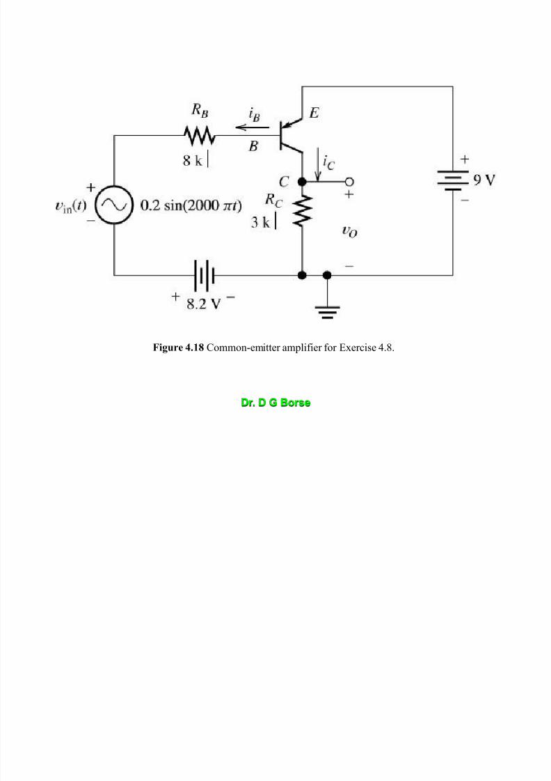
Figure 4.18 Common-emitter amplifier for Exercise 4.8.

7/27/2019 Bjt Basics 1
http://slidepdf.com/reader/full/bjt-basics-1 66/69
Dr. D G Borse
Figure 4.19a BJT large-signal models. ( Note: Values shown are appropriate for typical small-signal silicon devices at
a temperature of 300K.
7/27/2019 Bjt Basics 1
http://slidepdf.com/reader/full/bjt-basics-1 67/69
Dr. D G Borse
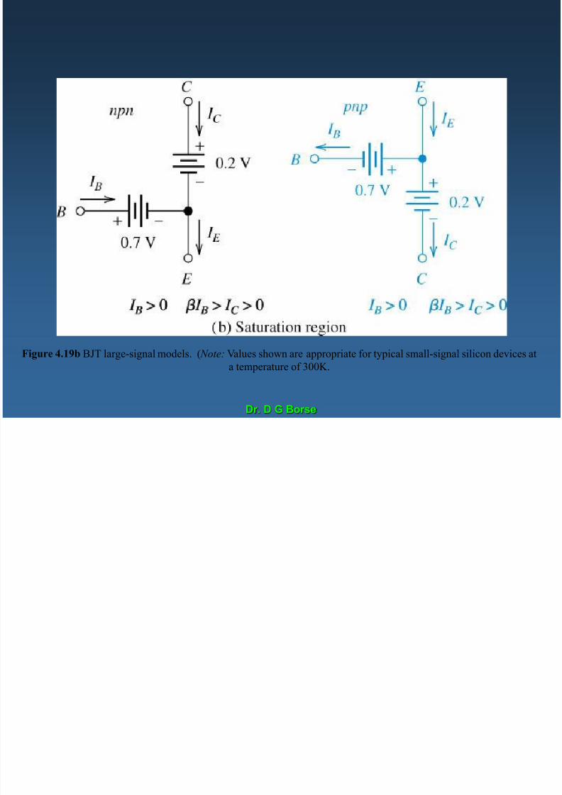
Figure 4.19b BJT large-signal models. ( Note: Values shown are appropriate for typical small-signal silicon devices at
a temperature of 300K.
7/27/2019 Bjt Basics 1
http://slidepdf.com/reader/full/bjt-basics-1 68/69
Dr. D G Borse
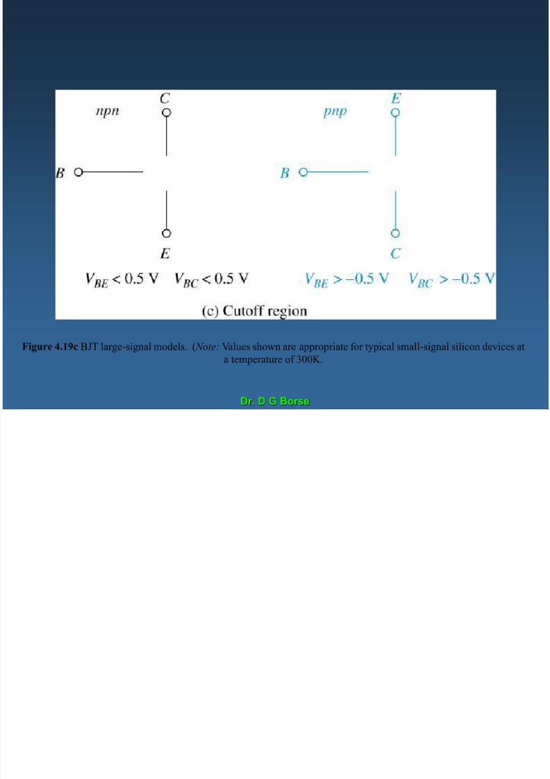
Figure 4.19c BJT large-signal models. ( Note: Values shown are appropriate for typical small-signal silicon devices at
a temperature of 300K.

7/27/2019 Bjt Basics 1
http://slidepdf.com/reader/full/bjt-basics-1 69/69


![Chp1 1 bjt [read only]](https://img.pdfslide.net/doc/110x75/5561fb4ad8b42ae04e8b4eba/chp1-1-bjt-read-only.jpg)