Embed Size (px)
Citation preview

© September 12, 2016 Dr. Lynn Fuller
BJT Characterization Laboratory
Page 1
Rochester Institute of Technology
Microelectronic Engineering
ROCHESTER INSTITUTE OF TECHNOLOGYMICROELECTRONIC ENGINEERING
BJT Characterization Laboratory
Dr. Lynn FullerElectrical and Microelectronic Engineering
Rochester Institute of Technology82 Lomb Memorial DriveRochester, NY 14623-5604
Tel (585) 475-2035Email: [email protected]
Dr. Fuller’s Webpage: http://people.rit.edu/lffeeeMicroE Webpage: http://www.rit.edu/kgcoe/microelectronic/
9-12-2016 Lab_BJT_Characterization.ppt
© September 12, 2016 Dr. Lynn Fuller
BJT Characterization Laboratory
Page 2
Rochester Institute of Technology
Microelectronic Engineering
OUTLINE
2N3904
BE Junction
BC Junction
IC-VCE Family of Curves
Beta at low, medium, high currents
SPICE Models
Temperature Effects

© September 12, 2016 Dr. Lynn Fuller
BJT Characterization Laboratory
Page 3
Rochester Institute of Technology
Microelectronic Engineering
DEFINITIONS
Bipolar Junction Transistor - (BJT) Both holes and electrons participate in the conduction of current, hence the name bipolar.
Minority carrier - In a p-type semiconductor electrons are the minority carrier type, in an n-type semiconductor holes are the minority carrier type.
Emitter - Emits minority carriers into the base region of a BJT. For example, in an NPN BJT the n-type emitter, emits electrons into the p-type base. The emitter usually has the highest doping levels of the three regions of a BJT.
Base - Thin region which is used to control the flow of minority carriers from the emitter to the collector
Collector -Collects the minority carriers that make it through the base from the emitter. The collector usually has the lightest doping concentrations of the three regions.
DC Beta ( bdc ) - The ratio of the collector current to the base current. bdc = IC / IBAC Beta ( bac ) - The ratio of the change in the collector current to the change in the base current. bac = D IC / D IB

© September 12, 2016 Dr. Lynn Fuller
BJT Characterization Laboratory
Page 4
Rochester Institute of Technology
Microelectronic Engineering
BJT - BIPOLAR JUNCTION TRANSISTOR
Flat
1
2
2N
3904
3
Label
1 = Emitter
2 = Base
3 = Collector

© September 12, 2016 Dr. Lynn Fuller
BJT Characterization Laboratory
Page 5
Rochester Institute of Technology
Microelectronic Engineering
SCHEMATIC SYMBOLS
npn
Emitter
Collector
Basen
p
n
Emitter
Collector
Base
pnp
Emitter
Collector
Basep
n
p
Emitter
Collector
Base
The arrow on the emitter is in the direction that
current will flow in the Base Emitter pn junction

© September 12, 2016 Dr. Lynn Fuller
BJT Characterization Laboratory
Page 6
Rochester Institute of Technology
Microelectronic Engineering
IDEALIZED STRUCTURE
n-type
p-type
n-type
Collector
Base
Emitter
SCSC
NN P

© September 12, 2016 Dr. Lynn Fuller
BJT Characterization Laboratory
Page 7
Rochester Institute of Technology
Microelectronic Engineering
ELECTRON CONCENTRATIONS IN AN NPN BJT
x
Base CollectorEmitter
n~Nden~Ndc
BE
Space Charge Layer
E
BC
n~very small but not zero
~ni2/Nab
With the B-E junction forward biased, and B-C junction reverse biased. There is a concentration gradient in the base that forces electrons to flow toward the collector.

© September 12, 2016 Dr. Lynn Fuller
BJT Characterization Laboratory
Page 8
Rochester Institute of Technology
Microelectronic Engineering
COMMENTS
1. The concentration of electrons in n-type silicon is ~ doping concentration in that region.2. In p-type silicon the number of electrons is almost zero3. A forward biased pn junction means more carriers of both types can cross the potential barrier. So a forward biased base-emitter junction (in an npn BJT) means more electrons on the base side than in equilibrium (no bias).4. A reverse biased pn junction means less carriers of both types can cross the potential barrier. So a reverse biased base-collector junction (in an npn BJT) means less electrons on the base side than in equilibrium (no bias). Even closer to zero electrons in p-type base at the edge of the B-C space charge layer.5. The base is so narrow that few electrons are lost as they diffuse across the base width. Diffusion is driven by a concentration gradient. So electrons move towards the collector and current flows in the opposite direction.

© September 12, 2016 Dr. Lynn Fuller
BJT Characterization Laboratory
Page 9
Rochester Institute of Technology
Microelectronic Engineering
2N3904
Flat
1
2
2N
3904
3
Label
Test Fixture

© September 12, 2016 Dr. Lynn Fuller
BJT Characterization Laboratory
Page 10
Rochester Institute of Technology
Microelectronic Engineering
HP4145B SEMICONDUCTOR PARAMETER ANALYZER

© September 12, 2016 Dr. Lynn Fuller
BJT Characterization Laboratory
Page 11
Rochester Institute of Technology
Microelectronic Engineering
TEST EQUIPMENT
Switch Matrix
Ultracision
Semi-Automatic
Wafer Prober
HP4145
Semiconductor Paramater
Analyzer
Computer
ICS (metrics)
Osprey
(video capture)
Microsoft Office
Test Fixture
and
Manual Probe Station
IEEE
488

© September 12, 2016 Dr. Lynn Fuller
BJT Characterization Laboratory
Page 12
Rochester Institute of Technology
Microelectronic Engineering
TEST STATION
HP4145 tester
Switch Matrix
PC Interface
Light Source
Semi-Auto
Probe Station
CCD Camera
Microscope

© September 12, 2016 Dr. Lynn Fuller
BJT Characterization Laboratory
Page 13
Rochester Institute of Technology
Microelectronic Engineering
OPERATION OF HP4145 AND SWITCH MATRIX
Turn on the HP4145, Switch Matrix, and PC
Select ICS icon on the desktop (close and message window)
Click on GPIB icon on the top of the screen select NI-32Thunk
Click on Instrument icon and select HP4145
Click on device icon and select PN Diode or BJT
Click on SMU1 then click on terminal (n-side of diode)
set SMU1 to zero volts ground
Click on SMU2 then click on terminal (p-side of diode)
set SMU2 to sweep from -10 to 10 Volts, measure
I and V
Click on done
Click on measure button
Wait for data to graph then add cursors, lines, titles, source conditions

© September 12, 2016 Dr. Lynn Fuller
BJT Characterization Laboratory
Page 14
Rochester Institute of Technology
Microelectronic Engineering
2N3904 DATA SHEET
Note: see page 12-15 of this document for more information on BJT SPICE parameters

© September 12, 2016 Dr. Lynn Fuller
BJT Characterization Laboratory
Page 15
Rochester Institute of Technology
Microelectronic Engineering
THEORETICAL BE JUNCTION, BC JUNCTION, CE
I
V
I
V
I
V0.7
-8
0.7
-8
0.7
-8
Emitter
BaseI
V
+
-
Collector
BaseI
V+
-
Emitter
I
V+
-
Collector
© September 12, 2016 Dr. Lynn Fuller
BJT Characterization Laboratory
Page 16
Rochester Institute of Technology
Microelectronic Engineering
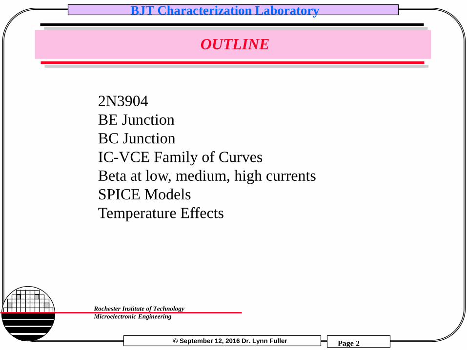
BE AND BC DIODE CHARACTERISTICS
Identify BE junction, measure ISE and VBE. Identify BC junction
and measure IS. Identify Base, Emitter,
Collector leads and label on sketch.
2N
39
04

© September 12, 2016 Dr. Lynn Fuller
BJT Characterization Laboratory
Page 17
Rochester Institute of Technology
Microelectronic Engineering
BETA MEASURED FROM FAMILY OF CURVES
Early Voltage is measured to be 116 for IC ~ 15 mA
Beta = 180 @ ~5mA
and Vce=5
Beta = 160 @
~15mA and Vce=5
Beta = 121 @
~40mA and Vce=5
Beta = 116 @
~0.02mA and Vce=5
Beta = 44 @ ~90mA
and Vce=5

© September 12, 2016 Dr. Lynn Fuller
BJT Characterization Laboratory
Page 18
Rochester Institute of Technology
Microelectronic Engineering
BETA VS IC – 2N3904
1ma 10ma 100ma
100
200
Measured
SPICE SIMULATED
BE
TA
Ic0.1ma .01ma
© September 12, 2016 Dr. Lynn Fuller
BJT Characterization Laboratory
Page 19
Rochester Institute of Technology
Microelectronic Engineering
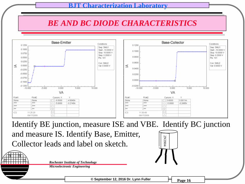
SPICE SIMULATED
BE
TA
Ic
SPICE ModelSPICE Simulatin of
Beta vs Ic
100
150
50
200
0 1mA 10mA 100mA100uA

© September 12, 2016 Dr. Lynn Fuller
BJT Characterization Laboratory
Page 20
Rochester Institute of Technology
Microelectronic Engineering
2N3904 SPICE MODEL
From the datasheet above
Why does the SPICE model have Bf of 416 when the maximum Bf=300
Answer: It is a model parameter and when combined with other model
parameters give correct results. See next page.

© September 12, 2016 Dr. Lynn Fuller
BJT Characterization Laboratory
Page 21
Rochester Institute of Technology
Microelectronic Engineering
BJT SPICE PARAMETERS EFFECT ON BETA
QRITNPN
NPN
BF 416
QRITNPN
NPN
BF 416
IKF .06678
QRITNPN
NPN
BF 416
IKF .06678
IS 6.734000E-15
ISE 6.734000E-15
NE 1.259
Ic
Ic
Ic
BE
TA
BE
TA
BE
TA
When BF=419 is used by
itself it gives incorrect
results200
200
200
Adding IS, ISE and NE
makes the model give
correct results for all IC
Adding IKF to the model
helps reduce BF at high IC

© September 12, 2016 Dr. Lynn Fuller
BJT Characterization Laboratory
Page 22
Rochester Institute of Technology
Microelectronic Engineering
IC=VCD FAMILY OF CURVES
QRITNPN
NPN
IS 6.734000E-15
BF 416
IKF .06678
ISE 6.734000E-15
NE 1.259
RB 10
RC 1
VA 109
SPICE SIMULATION
SPICE MODEL
IC
Vce

© September 12, 2016 Dr. Lynn Fuller
BJT Characterization Laboratory
Page 23
Rochester Institute of Technology
Microelectronic Engineering
2N3904 FORWARD ACTIVE
What is Beta?
What is VA?

© September 12, 2016 Dr. Lynn Fuller
BJT Characterization Laboratory
Page 24
Rochester Institute of Technology
Microelectronic Engineering
TEMPERATURE EFFECT ON FAMILY OF CURVES

© September 12, 2016 Dr. Lynn Fuller
BJT Characterization Laboratory
Page 25
Rochester Institute of Technology
Microelectronic Engineering
2N3904 INVERSE MODE
What is Beta?

© September 12, 2016 Dr. Lynn Fuller
BJT Characterization Laboratory
Page 26
Rochester Institute of Technology
Microelectronic Engineering
2N3904 VBE STEPS
What is gm?

© September 12, 2016 Dr. Lynn Fuller
BJT Characterization Laboratory
Page 27
Rochester Institute of Technology
Microelectronic Engineering
PNP FORWARD ACTIVE

© September 12, 2016 Dr. Lynn Fuller
BJT Characterization Laboratory
Page 28
Rochester Institute of Technology
Microelectronic Engineering
REFERENCES
1. MOSFET Modeling with SPICE, Daniel Foty, 1997, Prentice Hall, ISBN-0-13-227935-5
2. Operation and Modeling of the MOS Transistor, 2nd Edition, Yannis Tsividis, 1999, McGraw-Hill, ISBN-0-07-065523-5
3. UTMOST III Modeling Manual-Vol.1. Ch. 5. From Silvaco International.4. ATHENA USERS Manual, From Silvaco International.5. ATLAS USERS Manual, From Silvaco International.6. Device Electronics for Integrated Circuits, Richard Muller and Theodore
Kamins, with Mansun Chan, 3rd Edition, John Wiley, 2003, ISBN 0-471-59398-27. ICCAP Manual, Hewlet Packard8. PSpice Users Guide.
© September 12, 2016 Dr. Lynn Fuller
BJT Characterization Laboratory
Page 29
Rochester Institute of Technology
Microelectronic Engineering
LAB WORK USING HP4145
Obtain I-V plot for BE junctionObtain I-V plot for BC junctionObtain I-V plot for C-EObtain Ic-Vce family of curves for 2n3904 (for different Ib’s)Extract VA Early VoltageExtract Beta at 5 different IC values (0.1mA to 100mA)Obtain Ic-Vce family of curves at elevated temperatureObtain Ic-Vce family of curves for inverse operationExtract Beta InverseObtain Ic-Vce curves for different Vbe
Repeat some or all of above for 2N3906

© September 12, 2016 Dr. Lynn Fuller
BJT Characterization Laboratory
Page 30
Rochester Institute of Technology
Microelectronic Engineering
LABWORK – BJT CHARACTERIZATION
Use SPICE to obtain the following during lab:
1. Ic-Vce family of curves for 2N3904 (use Q2N3904 in BIPOLAR library).
2. Extract VA Early Voltage from family of curves.3. Extract Beta at 5 different IC values (0.1mA to 100mA)4. Obtain Ic-Vce family of curves at elevated temperature5. Obtain Ic-Vce family of curves for inverse operation6. Extract Beta Inverse from family of curves.7. Obtain Ic-Vce curves for different Vbe8. Obtain Ic-Vce family of curves for 2N3906 (PNP) transistor.
No Lab Report