Embed Size (px)
Citation preview

BME-328 Lab-7 1
----------------------------------------------------------------------------------------------------------
BME328 LAB7
Implementation of Simple Processor
40 Marks (3 weeks) Due Date: Week 13
-----------------------------------------------------------------------------------------------------------
Objective:
• Design and implementation of simple 8-bit microprocessor • The processor consists of ALU, Registers to store data, Control unit to execute
instructions pointed to by program counter (PC)
Summary of System Operation:
An abstract view of system is illustrated in Fig.1.
1. 8-bit input data is entered in the simulation phase through the Quartus II
waveform editor, and stored in register R1 when instruction LD-R1 is executed 2. 8-bit ALU perform operation on input A and input B based on OP code of
executed instruction 3. ALU input A is connected to R1, input B is connected to Accumulator AC. 4. Results of each operation is displayed on two 7 Seg display unit connected to
output of AC 5. RC register stores 8-bit input data when LD-RC instruction is executed and RC
output is used as a conditional register for control flow 6. PC is a counter that is used to point to next instruction to be executed and starts
from Instruction 0 to Instruction N. Each clock cycle it increments PC to point
to next instruction 7. Combinational circuit stores the Instructions starting from address 0 to address
N. Each instruction has its op code to be used by ALU.

BME-328 Lab-7 2
Fig.1 SIMPLE PROCESSOR Organization
Lab Procedure:
This processor consists of different components that functions in specific sequence to
generate the desired output according to the instruction being executed. A processor is
usually divided to 4 distinct sub-units Memory Unit, Control Unit, Data storage and ALU
core unit. The Memory Unit performs the fetching of instructions. Data storage unit
stores data from input switches and results of ALU unit to registers R1, RC and Acc. The
ALU Core performs the arithmetic and logical operations on desired inputs and produces
the required outputs. The Control unit decode the instruction and activates the control
signals to execute it. In this project, we will be implementing distinct tasks by varying
logic of control unit.
BME-328 Lab-7 3
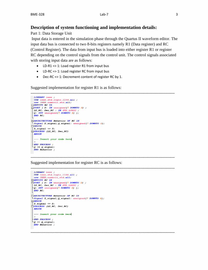
Description of system functioning and implementation details:
Part 1: Data Storage Unit
Input data is entered in the simulation phase through the Quartus II waveform editor. The
input data bus is connected to two 8-bits registers namely R1 (Data register) and RC
(Control Register). The data from input bus is loaded into either register R1 or register
RC depending on the control signals from the control unit. The control signals associated
with storing input data are as follows:
• LD-R1 => 1: Load register R1 from input bus
• LD-RC => 1: Load register RC from input bus
• Dec-RC => 1: Decrement content of register RC by 1.
Suggested implementation for register R1 is as follows:
----------------------------------------------------------------------------------------------------------
----------------------------------------------------------------------------------------------------------
Suggested implementation for register RC is as follows:
----------------------------------------------------------------------------------------------------------
----------------------------------------------------------------------------------------------------------

BME-328 Lab-7 4
Part 2: Arithmetic Logic Unit Core
The heart of every processor unit is the ALU core where all arithmetic and logical
operations are to be implemented and applied as required. In this part students are
required to implement all functionalities and operations using VHDL syntax compatible
with Altera FPGA boards. ALU core consists of two components ALU and accumulator
(ACC). ACC is a register in which intermediate arithmetic and logic results are stored
and fed back to the ALU.
The ALU will take two 8-bit inputs (A and B) and a 4-bit opcode from Control unit. The
opcode input from controller unit is the operation-selector signal, deciding the operation
that is to be applied on the inputs A and B based on the instruction being executed.

BME-328 Lab-7 5
Suggested implementation for ALU is as follows:
----------------------------------------------------------------------------------------------------------
----------------------------------------------------------------------------------------------------------
Suggested implementation for ACC is as follows:
----------------------------------------------------------------------------------------------------------
----------------------------------------------------------------------------------------------------------

BME-328 Lab-7 6
Part 3: Control Unit
The Control unit decides the microcode that is to be delivered to the ALU core and will act as the
operations-selector for the ALU core. The Control Unit produces an output OP, which is passed
to ALU core as the operations selector. This component consists of program counter (PC) and
combinational circuit. The control unit uses Finite State Machine (FSM) to implement PC and
combinational circuit is an instruction memory. The details of instruction set to be implemented
by control unit are given in following table.
Instruction Set
Mnemonics Description Opcode
Register Transfer
LDR1 Load R1 from input; R1=INPUT 0
LDRC Load RC from input; RC= INPUT 1
Arithmetic Operations:
ADDA Add R1 to Acc; Acc= Acc + R1 2
SUBA Sub R1 from Acc; Acc= ACC-R1 3
INCA Increment Acc; Acc=Acc + 1 4
DECA Dec Acc; Acc= Acc -1 5
DEC-RC Dec RC; RC= RC-1 6
Logic Operations
ANDA And Acc with R1; Acc=Acc&R1 7
ORA Or Acc with R1; Acc = Acc | R1 8
XORA XOR Acc with R1; Acc =Acc XOR R1 9
NAND Invert Acc; Acc = Acc NAND R1 A
SLA Shift Left Acc; Acc=Acc*2 B
SRA Shift Right Acc; Acc = Acc/2 C
Control flow
BNEQZ branch to start if RC !=0; goto state D

BME-328 Lab-7 7
Task-1: Calculate average of 4 numbers entered from input x1, x2, x3, x4
Instruction Sequence to execute the task-1
Sequence
No.
Instruction Result from execution of the instruction
1 LDR1 0 R1 =0;
2 ANDA Acc=0
3 LDR1 X1 R1=X1
4 ADD Acc=X1
5 LDR1 X2 R1=X2
6 ADD Acc= X1+X2
7 LDR1 X3 R1=X3
8 ADD Acc=X1+X2+X3
9 LDR1 X4 R1=X4
10 ADD ACC=X1+X2+X3+X4
11 SR Acc= (X1+X2+X3+X4)/2
12 SR
Acc= (X1+X2+X3+X4)/4
FSM implementation of PC for task-1

BME-328 Lab-7 8
Suggested implementation of PC and instruction memory for task-1 is as follows: Please
note that next two figures are part of a single vhdl code file. Please focus on bottom of
first figure and top of second figure to find continuation between them.
----------------------------------------------------------------------------------------------------------

BME-328 Lab-7 9
----------------------------------------------------------------------------------------------------------
Task- 2:
Executing a Loop for number of times. For example
𝑓𝑜𝑟 (𝑖 = 5 ; 𝑖 ≥ 0 ; 𝑖 − −) {𝑟𝑒𝑠𝑢𝑙𝑡 = 𝑟𝑒𝑠𝑢𝑙𝑡 + 𝑥}
Instruction Sequence to execute the task-2
Sequence
No.
Instruction Result from execution of the instruction
1 LDRC 5 RC =5;
2 LDR1 0 R1=0
3 ANDA ACC=ACC and 0; ACC = 0;
4 LDR1 X R1= X
5 LOOP: ADD ACC = ACC+R1
6 DECRC RC = RC-1;
7 BNEQZ LOOP PC = address of “LOOP”

BME-328 Lab-7 10
FSM implementation of PC for task-2
Suggested implementation of PC and instruction memory for task-2 is as follows: Please
note that next two figures are part of a single vhdl code file. Please focus on bottom of
first figure and top of second figure to find continuation between them.
----------------------------------------------------------------------------------------------------------

BME-328 Lab-7 11
----------------------------------------------------------------------------------------------------------
Displaying Output
The final result of the task which corresponds to the content of ACC during final state of
task sequence should be clearly displayed in the simulation waveforms. Please refer to
the final schematic on the following page.

BME-328 Lab-7 12

BME-328 Lab-7 13
Assigned Tasks: -
Logic Operations: -
1-Enter X1, X2, X3, X4 from switches then perform the following: -
Result= (X1 AND X2) OR X3; Sum of products function
2-Enter X1, X2, X3, X4 from switches then perform the following: -
Result= (X1 OR X2) AND X3; Product of sums function
3-Enter X, Y from switches then perform the following: -
Result= (X XNOR Y); A comparator if(X=Y) Result=1;
Arithmetic Operations: -
1-Enter X1, X2, X3, X4 from switches then perform the following: -
Result= 2*(X1+X2+X3+X4); ADD then SHL
2-Enter X1, X2, Y1, Y2 from switches then perform the following: -
Result= (X1-Y1) + (X2-Y2); Difference between two sets of numbers
3-Enter X1, X2, X3, X4 from switches then perform the following: -
Result= (X1+1) + (X2+1) + (X3+1) + (X4+1); Inc each number and find total
4-Enter X1, Y1, X2, Y2 from switches then perform the following: -
Result= 2*(X1-Y1) +2*(X2-Y2); Calculate double the difference between two sets