Embed Size (px)
Citation preview

Bonding
Primary bonding
• ionic
• covalent
• polar covalent
• metallic
10 THE STRUCTURE OF MATERIALS
The excess binding energy, in turn, is related to a measurable quantity, namely thebond dissociation energy between two atoms, DE ij :
!A−B = DE AB − [(DE AA)(DE BB)]1/2 (1.7)
The bond dissociation energy is the energy required to separate two bonded atoms(see Appendix 1 for typical values). The greater the electronegativity difference, thegreater the excess binding energy. These quantities give us a method of characterizingbond types. More importantly, they relate to important physical properties, such asmelting point (see Table 1.5). First, let us review the bond types and characteristics,then describe each in more detail.
1.0.3.1 Primary Bonds. Primary bonds, also known as “strong bonds,” are createdwhen there is direct interaction of electrons between two or more atoms, either throughtransfer or as a result of sharing. The more electrons per atom that take place in this pro-cess, the higher the bond “order” (e.g., single, double, or triple bond) and the strongerthe connection between atoms. There are four general categories of primary bonds:ionic, covalent, polar covalent, and metallic. An ionic bond, also called a heteropolar
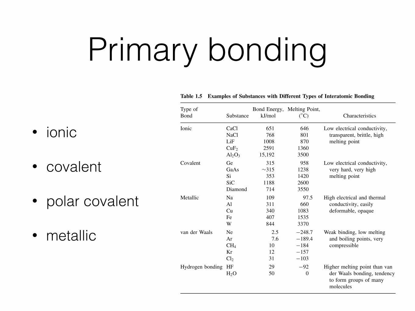
Table 1.5 Examples of Substances with Different Types of Interatomic Bonding
Type ofBond Substance
Bond Energy,kJ/mol
Melting Point,(◦C) Characteristics
Ionic CaCl 651 646 Low electrical conductivity,NaCl 768 801 transparent, brittle, highLiF 1008 870 melting pointCuF2 2591 1360Al2O3 15,192 3500
Covalent Ge 315 958 Low electrical conductivity,GaAs ∼315 1238 very hard, very highSi 353 1420 melting pointSiC 1188 2600Diamond 714 3550
Metallic Na 109 97.5 High electrical and thermalAl 311 660 conductivity, easilyCu 340 1083 deformable, opaqueFe 407 1535W 844 3370
van der Waals Ne 2.5 −248.7 Weak binding, low meltingAr 7.6 −189.4 and boiling points, veryCH4 10 −184 compressibleKr 12 −157Cl2 31 −103
Hydrogen bonding HF 29 −92 Higher melting point than vanH2O 50 0 der Waals bonding, tendency
to form groups of manymolecules
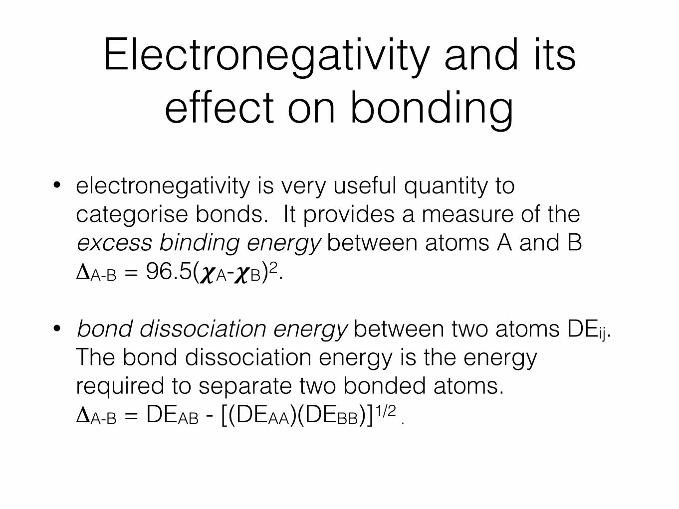
Electronegativity and its effect on bonding
• electronegativity is very useful quantity to categorise bonds. It provides a measure of the excess binding energy between atoms A and B ΔA-B = 96.5(𝝌A-𝝌B)2.
• bond dissociation energy between two atoms DEij. The bond dissociation energy is the energy required to separate two bonded atoms. ΔA-B = DEAB - [(DEAA)(DEBB)]1/2 .
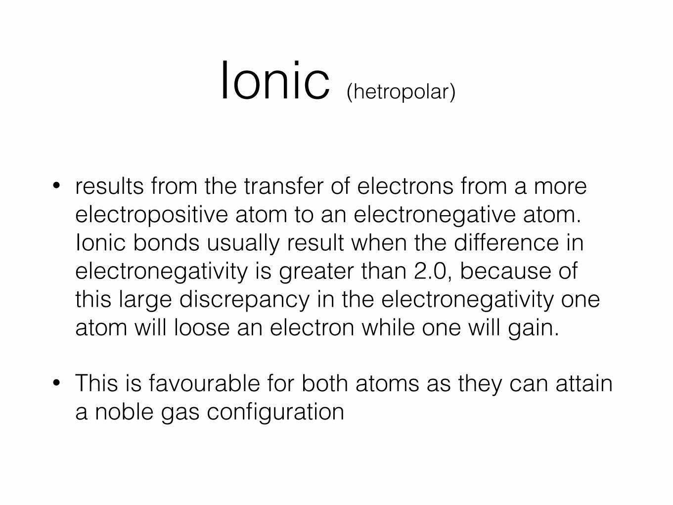
Ionic (hetropolar)
• results from the transfer of electrons from a more electropositive atom to an electronegative atom. Ionic bonds usually result when the difference in electronegativity is greater than 2.0, because of this large discrepancy in the electronegativity one atom will loose an electron while one will gain.
• This is favourable for both atoms as they can attain a noble gas configuration
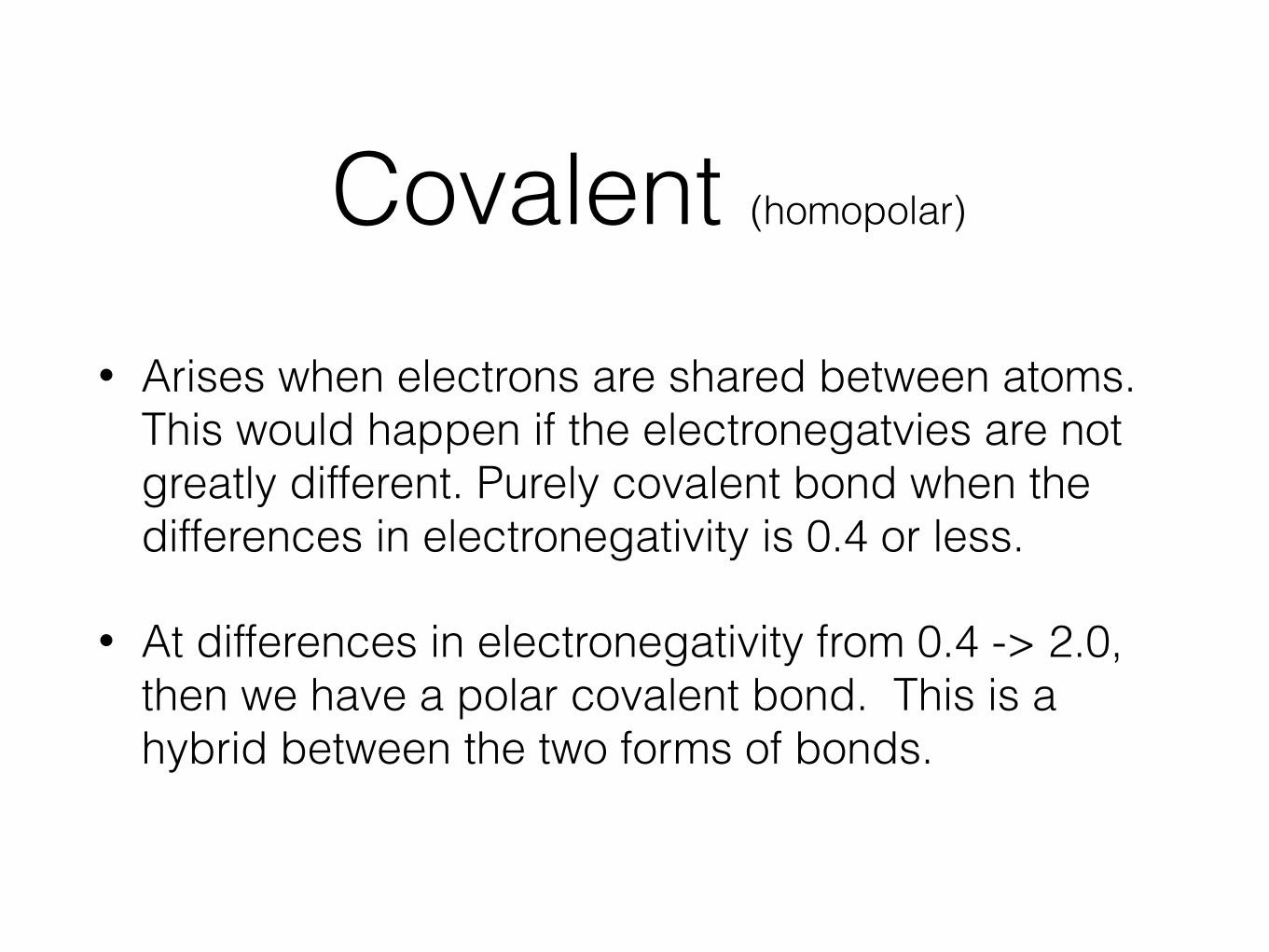
Covalent (homopolar)
• Arises when electrons are shared between atoms. This would happen if the electronegatvies are not greatly different. Purely covalent bond when the differences in electronegativity is 0.4 or less.
• At differences in electronegativity from 0.4 -> 2.0, then we have a polar covalent bond. This is a hybrid between the two forms of bonds.
Ionisation energy
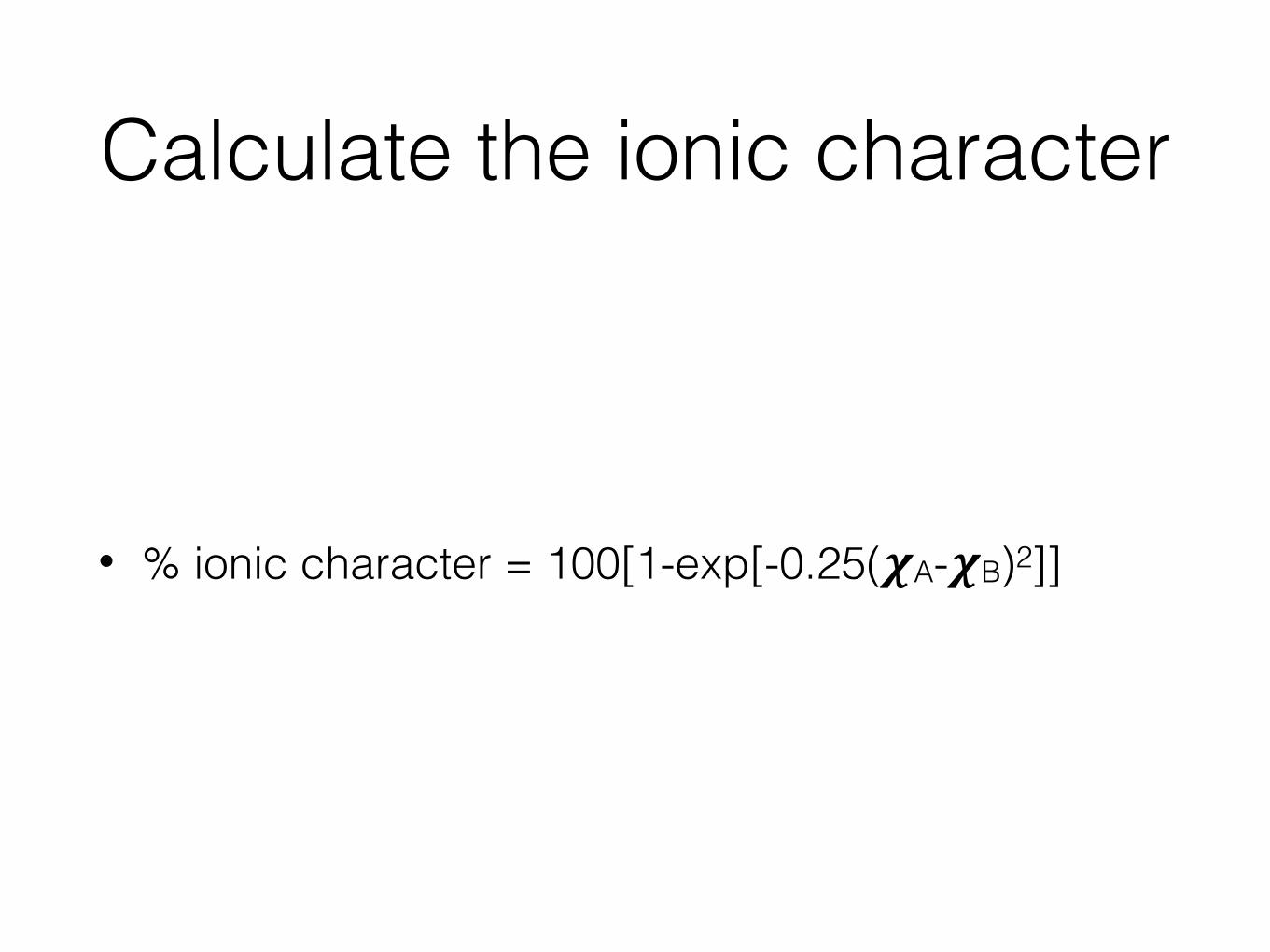
Calculate the ionic character
• % ionic character = 100[1-exp[-0.25(𝝌A-𝝌B)2]]
Question
• What is the percent ionic character of H-F?
55%
Metallic bond
• Bonding electrons become delocalised. Formed by atoms of low electronegativity. Model first proposed by Lorentz, uses a sea of electrons known as an ‘electron gas’
as its bulk density ror bulk dielectric constant 3. Such “mediumeffects” or “solvent effects”necessarily involve the simultaneous interactions of many molecules, both solvent andsolute, and they become particularly severe when dealing with short-range interactions
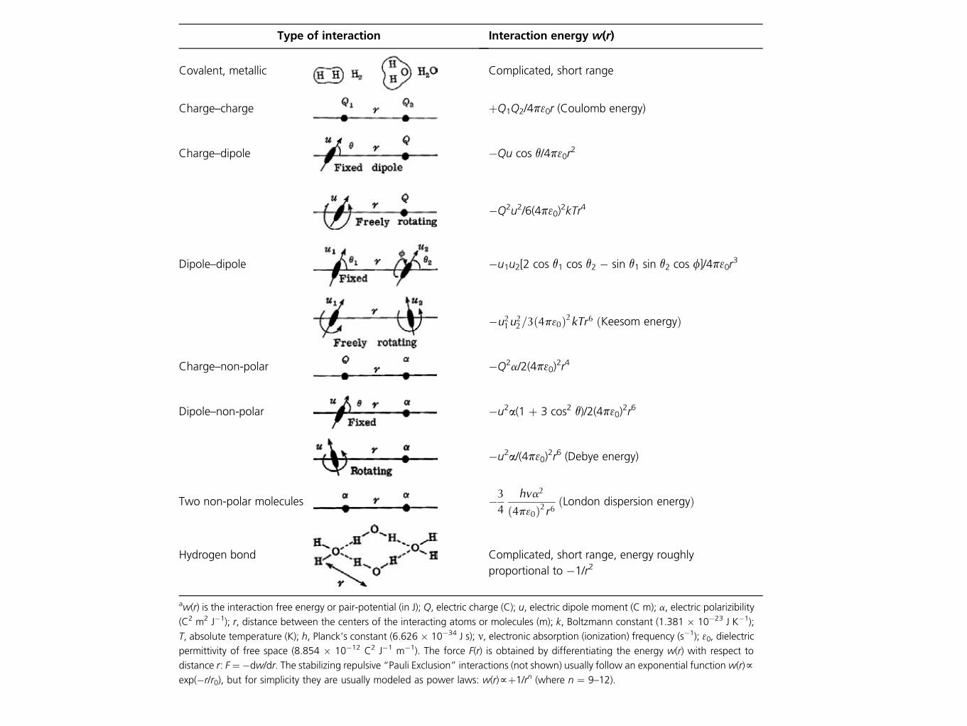
Table 2.2 Common Types of Interactions and their Pair-Potentials w(r) between TwoAtoms, Ions, or Small Molecules in a Vacuum (3 ¼ 1)a
Type of interaction Interaction energy w(r)
Covalent, metallic Complicated, short range
Charge–charge þQ1Q2/4p30r (Coulomb energy)
Charge–dipole #Qu cos q/4p30r2
#Q2u2/6(4p30)2kTr4
Dipole–dipole #u1u2[2 cos q1 cos q2 # sin q1 sin q2 cos f]/4p30r3
#u21u
22=3ð4p30Þ
2kTr6 ðKeesom energyÞ
Charge–non-polar #Q2a/2(4p30)2r4
Dipole–non-polar #u2a(1 þ 3 cos2 q)/2(4p30)2r6
#u2a/(4p30)2r6 (Debye energy)
Two non-polar molecules #3
4
hva2
ð4p30Þ2r6ðLondon dispersion energyÞ
Hydrogen bond Complicated, short range, energy roughlyproportional to #1/r2
aw(r) is the interaction free energy or pair-potential (in J); Q, electric charge (C); u, electric dipole moment (C m); a, electric polarizibility(C2 m2 J#1); r, distance between the centers of the interacting atoms or molecules (m); k, Boltzmann constant (1.381 & 10#23 J K#1);T, absolute temperature (K); h, Planck’s constant (6.626 & 10#34 J s); n, electronic absorption (ionization) frequency (s#1); 30, dielectricpermittivity of free space (8.854 & 10#12 C2 J#1 m#1). The force F(r) is obtained by differentiating the energy w(r) with respect todistance r: F¼#dw/dr. The stabilizing repulsive “Pauli Exclusion” interactions (not shown) usually follow an exponential function w(r)fexp(#r/r0), but for simplicity they are usually modeled as power laws: w(r)fþ1/rn (where n ¼ 9–12).
36 INTERMOLECULAR AND SURFACE FORCES

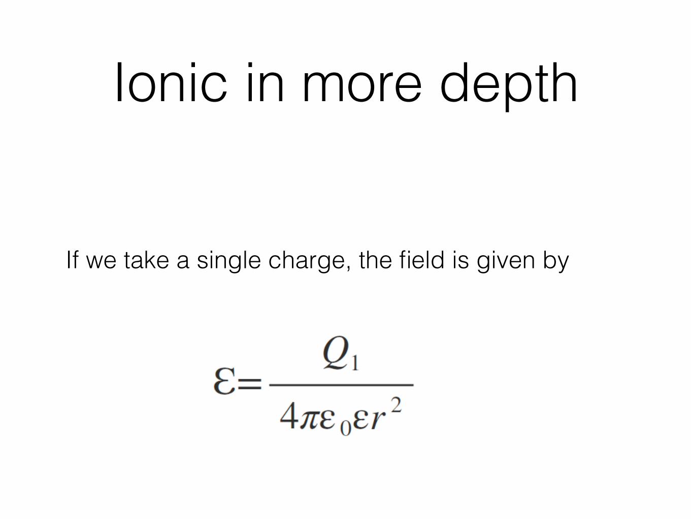
Ionic in more depth
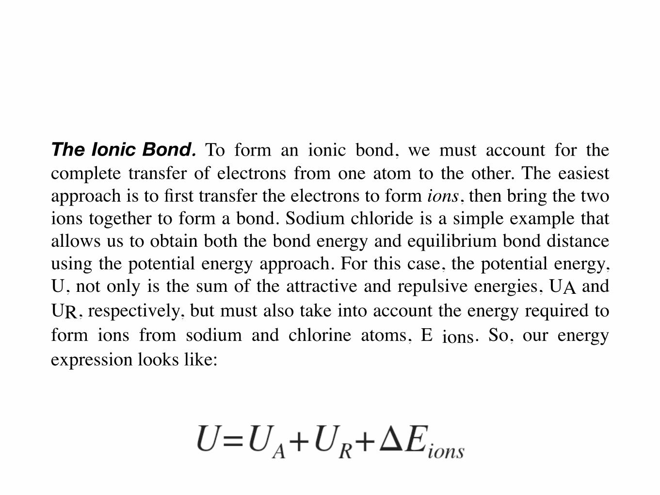
The Ionic Bond. To form an ionic bond, we must account for the complete transfer of electrons from one atom to the other. The easiest approach is to first transfer the electrons to form ions, then bring the two ions together to form a bond. Sodium chloride is a simple example that allows us to obtain both the bond energy and equilibrium bond distance using the potential energy approach. For this case, the potential energy, U, not only is the sum of the attractive and repulsive energies, UA and UR, respectively, but must also take into account the energy required to form ions from sodium and chlorine atoms, E ions. So, our energy expression looks like:
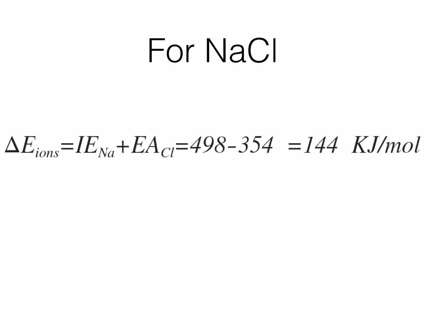
For NaCl
Ionic in more depth
If we take a single charge, the field is given by
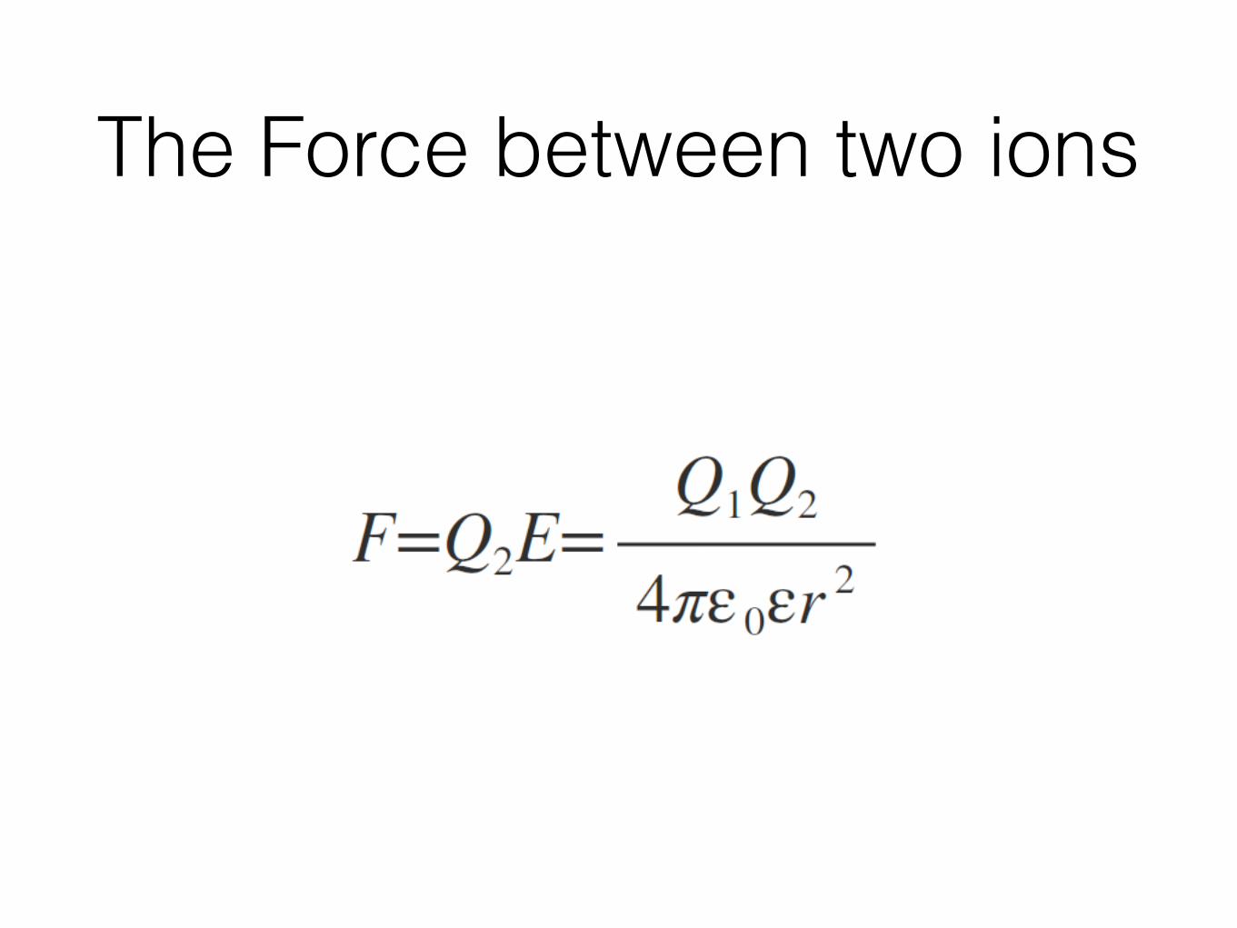
The Force between two ions
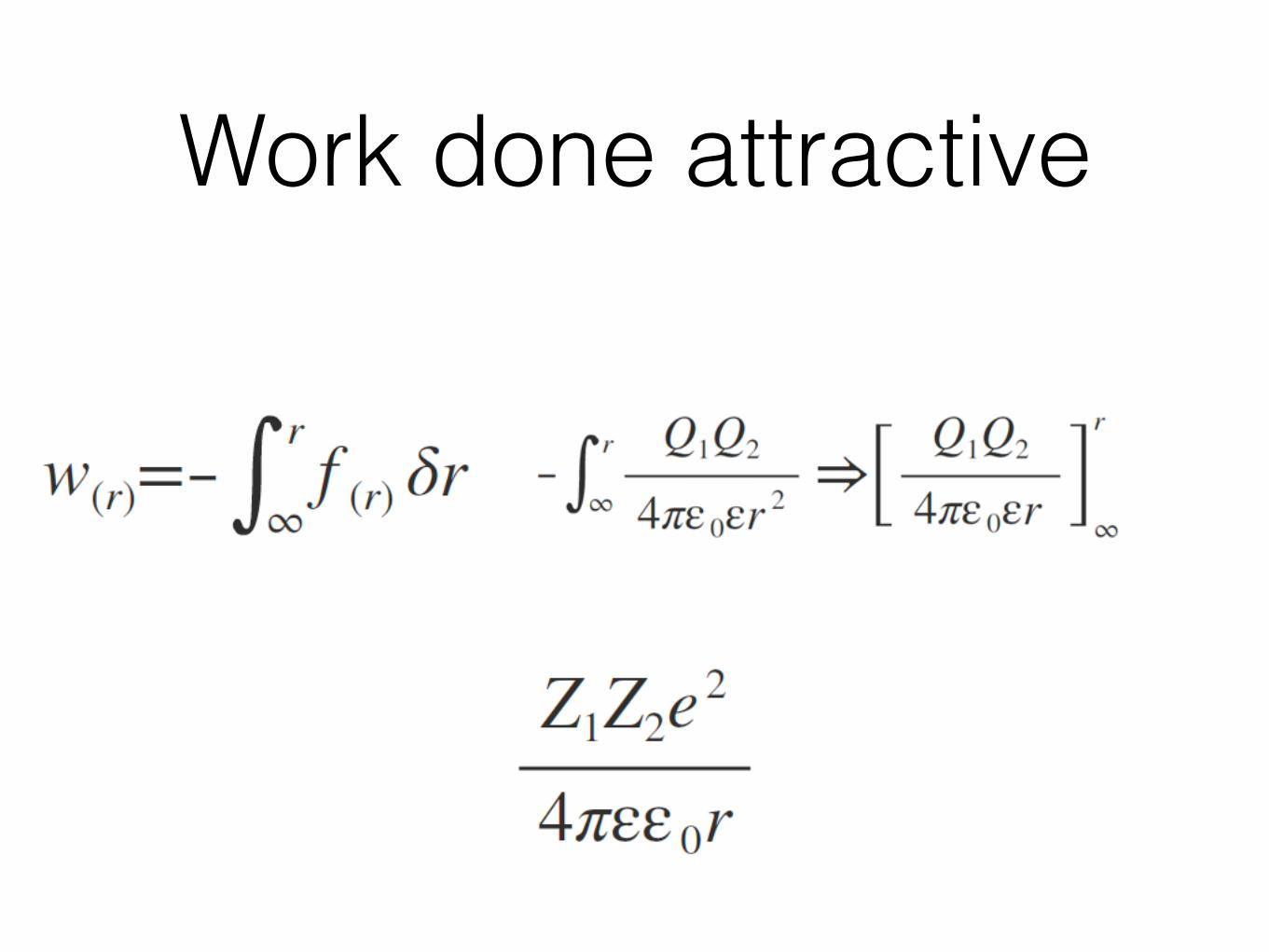
Work done attractive
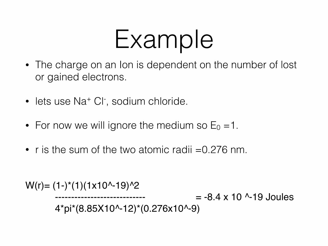
Example• The charge on an Ion is dependent on the number of lost
or gained electrons.
• lets use Na+ Cl-, sodium chloride.
• For now we will ignore the medium so E0 =1.
• r is the sum of the two atomic radii =0.276 nm.
W(r)= (1-)*(1)(1x10^-19)^2 ---------------------------- = -8.4 x 10 ^-19 Joules 4*pi*(8.85X10^-12)*(0.276x10^-9)
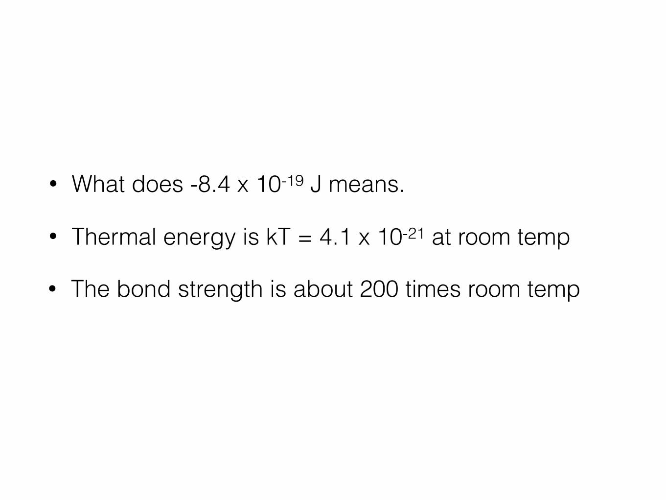
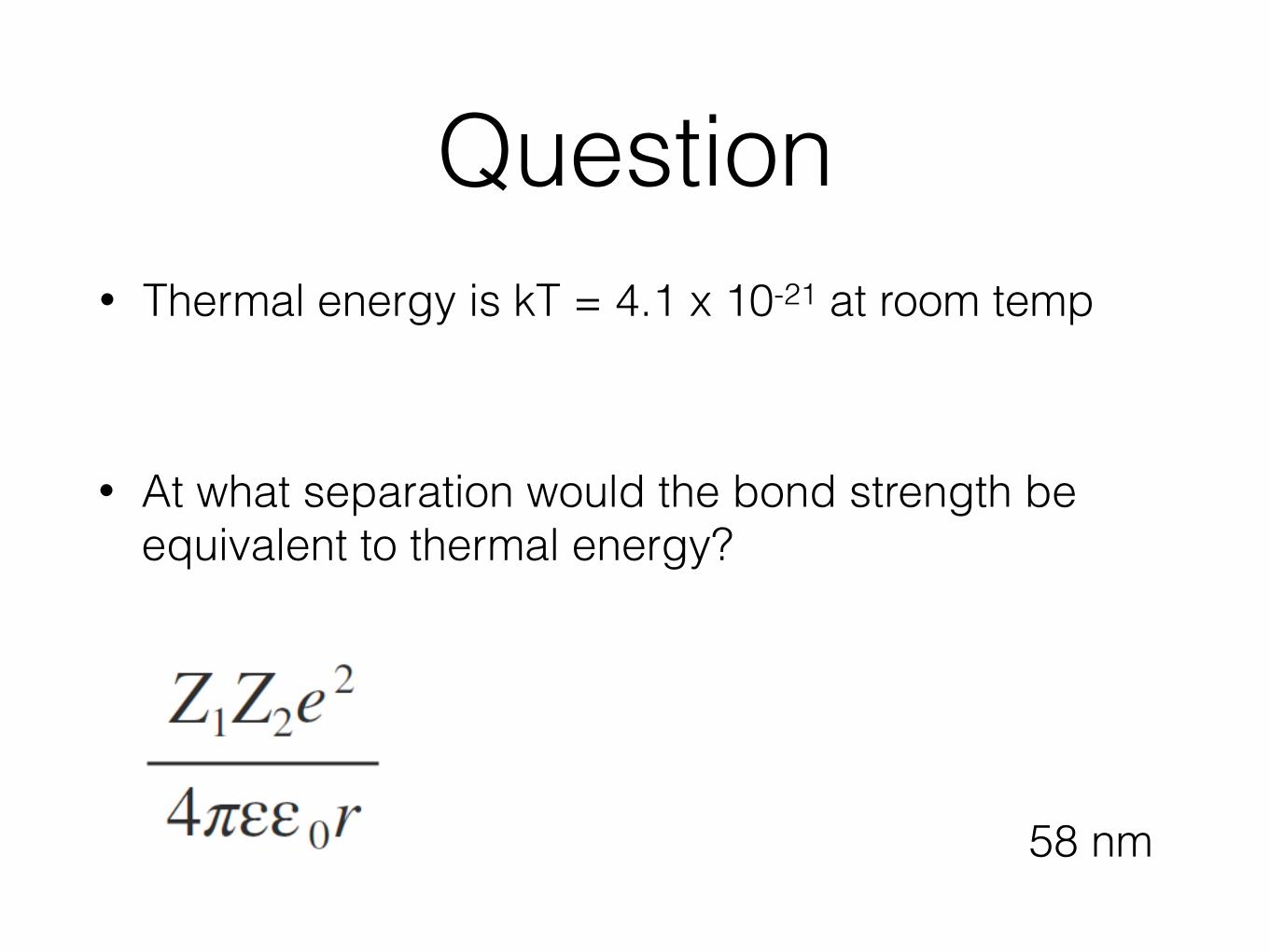
• Thermal energy is kT = 4.1 x 10⁻²¹ at room temp
• What does -8.4 x 10⁻¹⁹ J means.
• The bond strength is about 200 times room temp
Question
• At what separation would the bond strength be equivalent to thermal energy?
58 nm
• Thermal energy is kT = 4.1 x 10⁻²¹ at room temp
Question
• What is the force required to break an ionic bond?
What do we know now?
• Ionic bonds much stronger than thermal energy
• Non-Directional (why is this important)
• Quite long range (again why is this important)
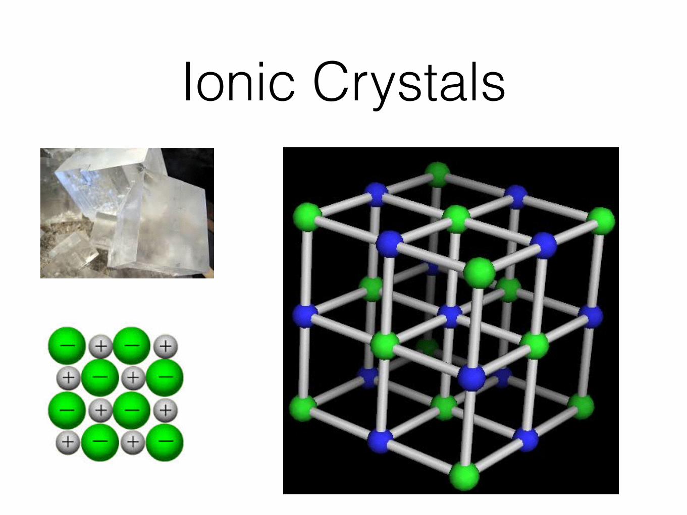
Ionic Crystals
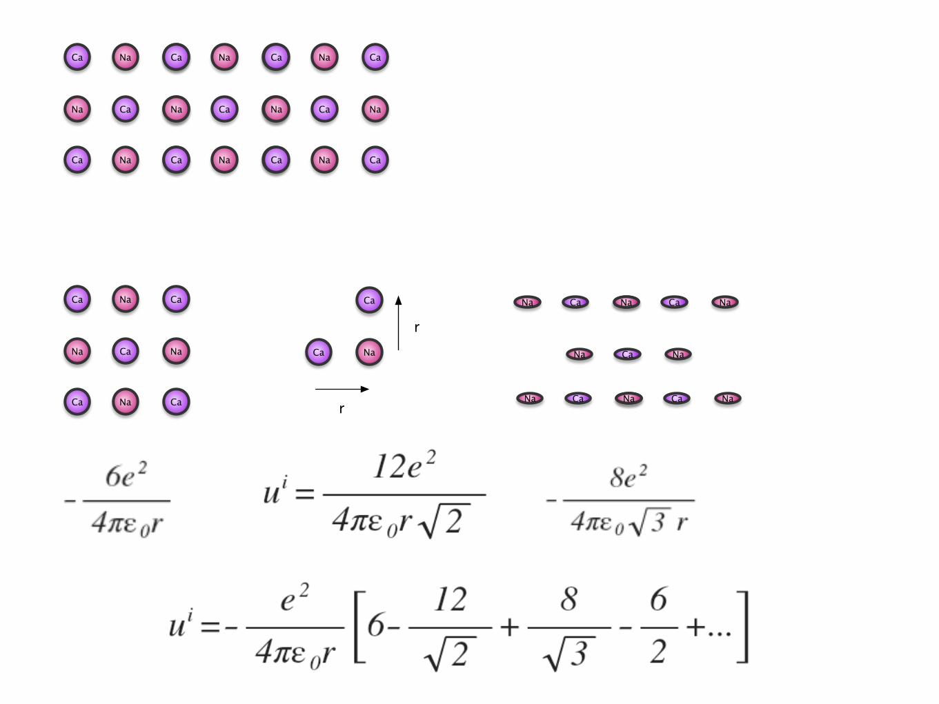
Na Ca
Na
Na
Na
Ca
Ca
Ca
Ca
Na Ca
Na
Na
Na
Ca
Ca
Ca
Ca
Na Ca
Na
Na
Na
Ca
Ca
Ca
Ca
Ca Na
Ca
r
r
Na Ca
Na
Na
Na
Ca
Ca
Ca
Ca
Na Ca Na
Na Ca Na
Na Ca Na
Na Ca Na
Na Ca Na
Madelung Constant
• Different for differing crystal structures.
• Varies from 1.638 -> 1.763
• Very difficult to calculate.
• crystals are more stable
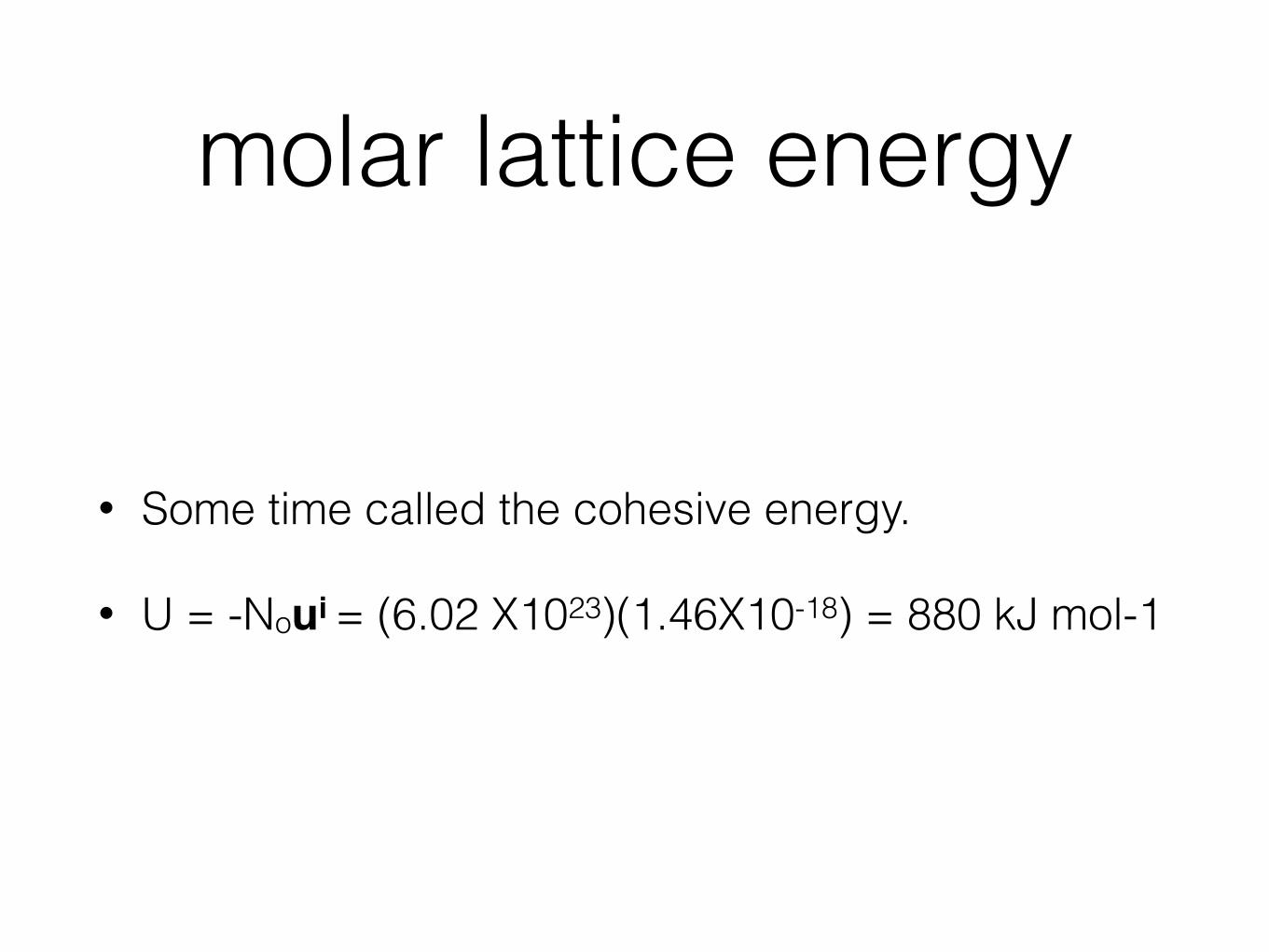
molar lattice energy
• Some time called the cohesive energy.
• U = -Noui = (6.02 X10²³)(1.46X10⁻¹⁸) = 880 kJ mol-1
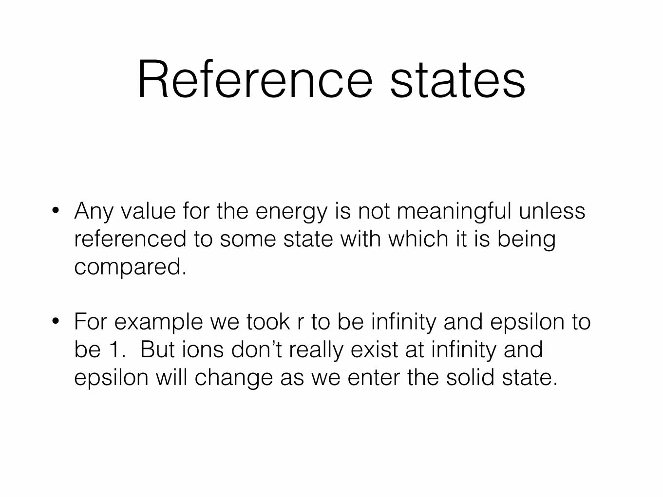
Reference states
• Any value for the energy is not meaningful unless referenced to some state with which it is being compared.
• For example we took r to be infinity and epsilon to be 1. But ions don’t really exist at infinity and epsilon will change as we enter the solid state.
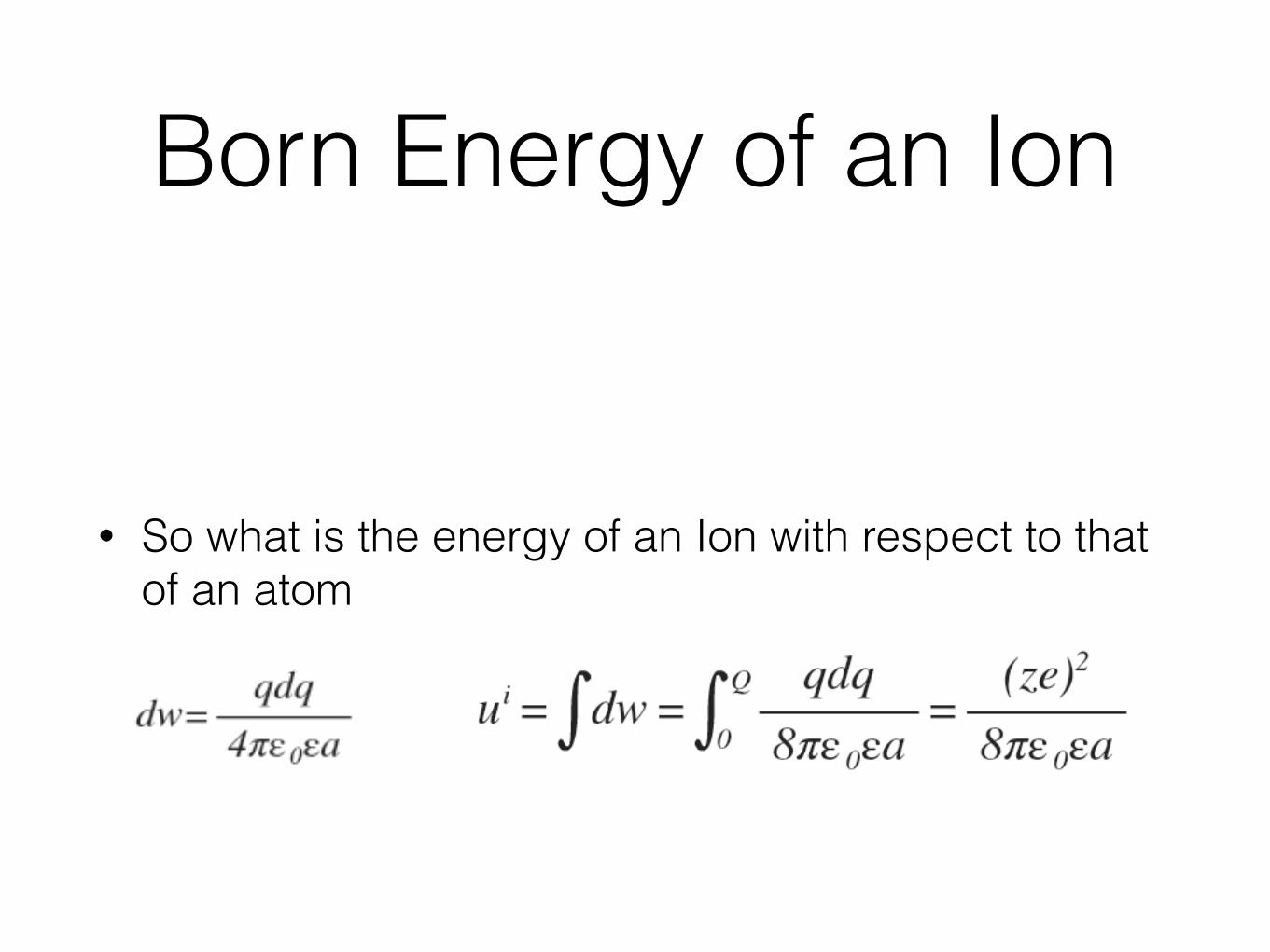
Born Energy of an Ion
• So what is the energy of an Ion with respect to that of an atom
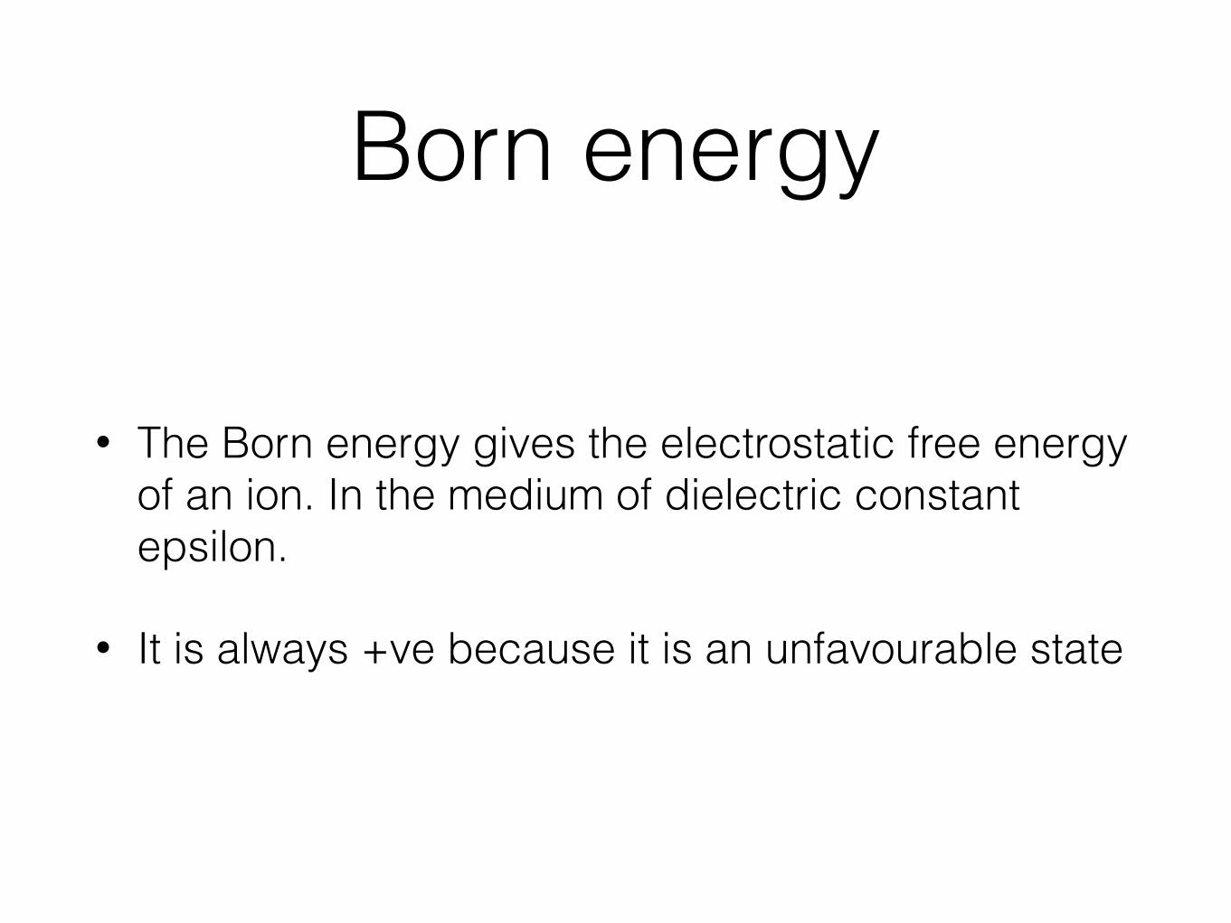
Born energy
• The Born energy gives the electrostatic free energy of an ion. In the medium of dielectric constant epsilon.
• It is always +ve because it is an unfavourable state
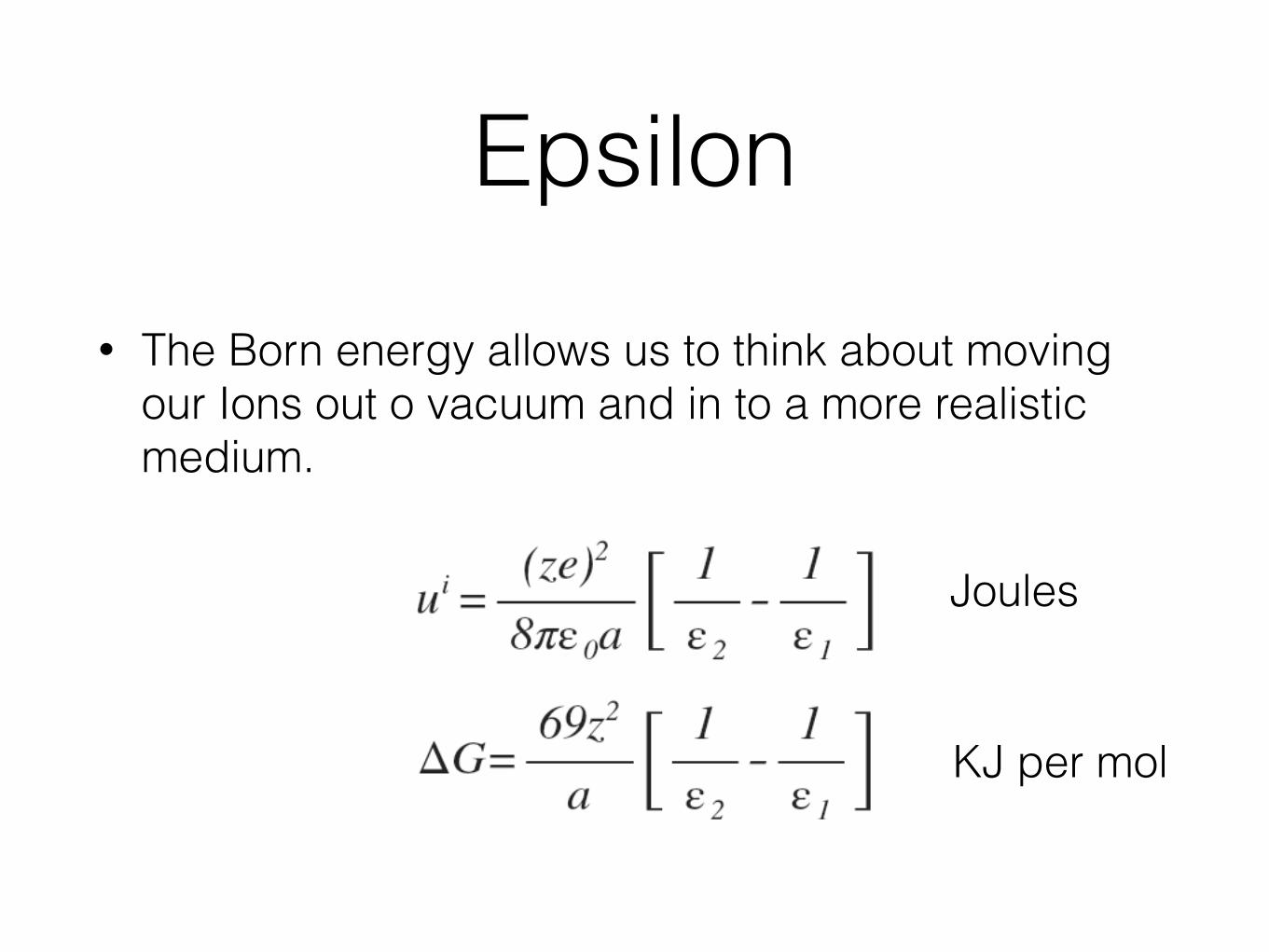
Epsilon• The Born energy allows us to think about moving
our Ions out o vacuum and in to a more realistic medium.
Joules
KJ per mol
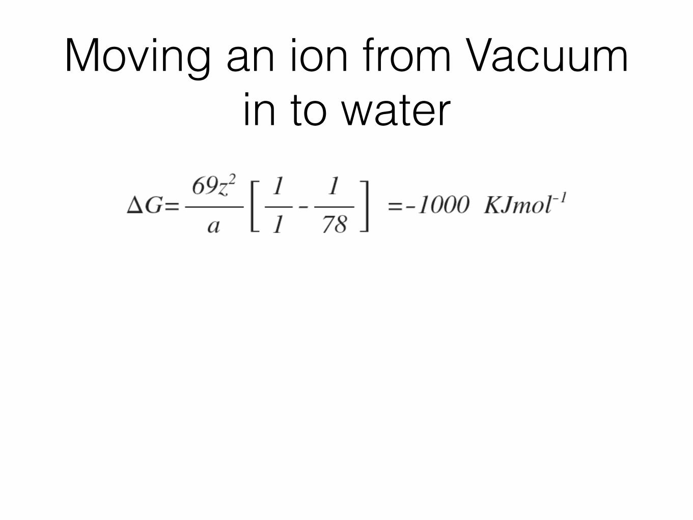
Moving an ion from Vacuum in to water
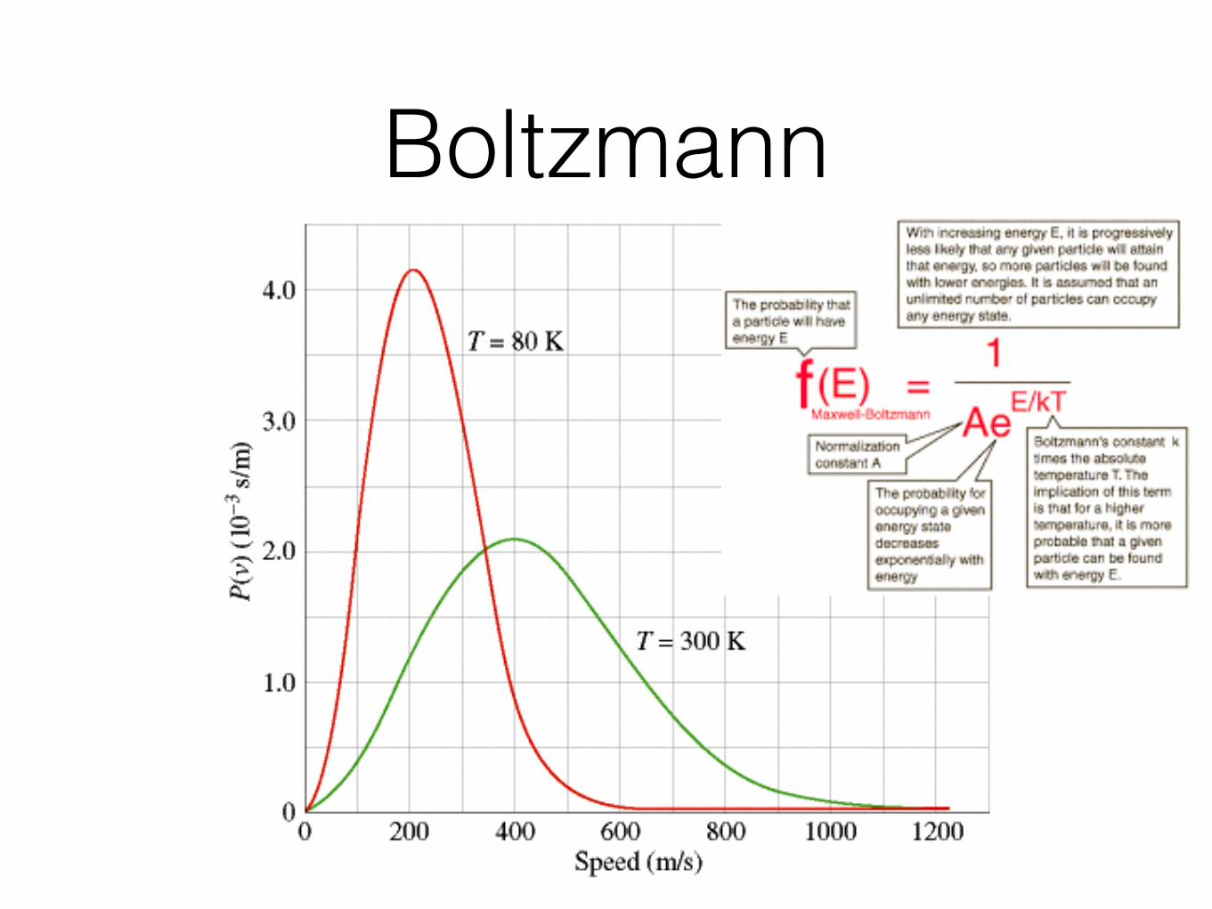
Boltzmann
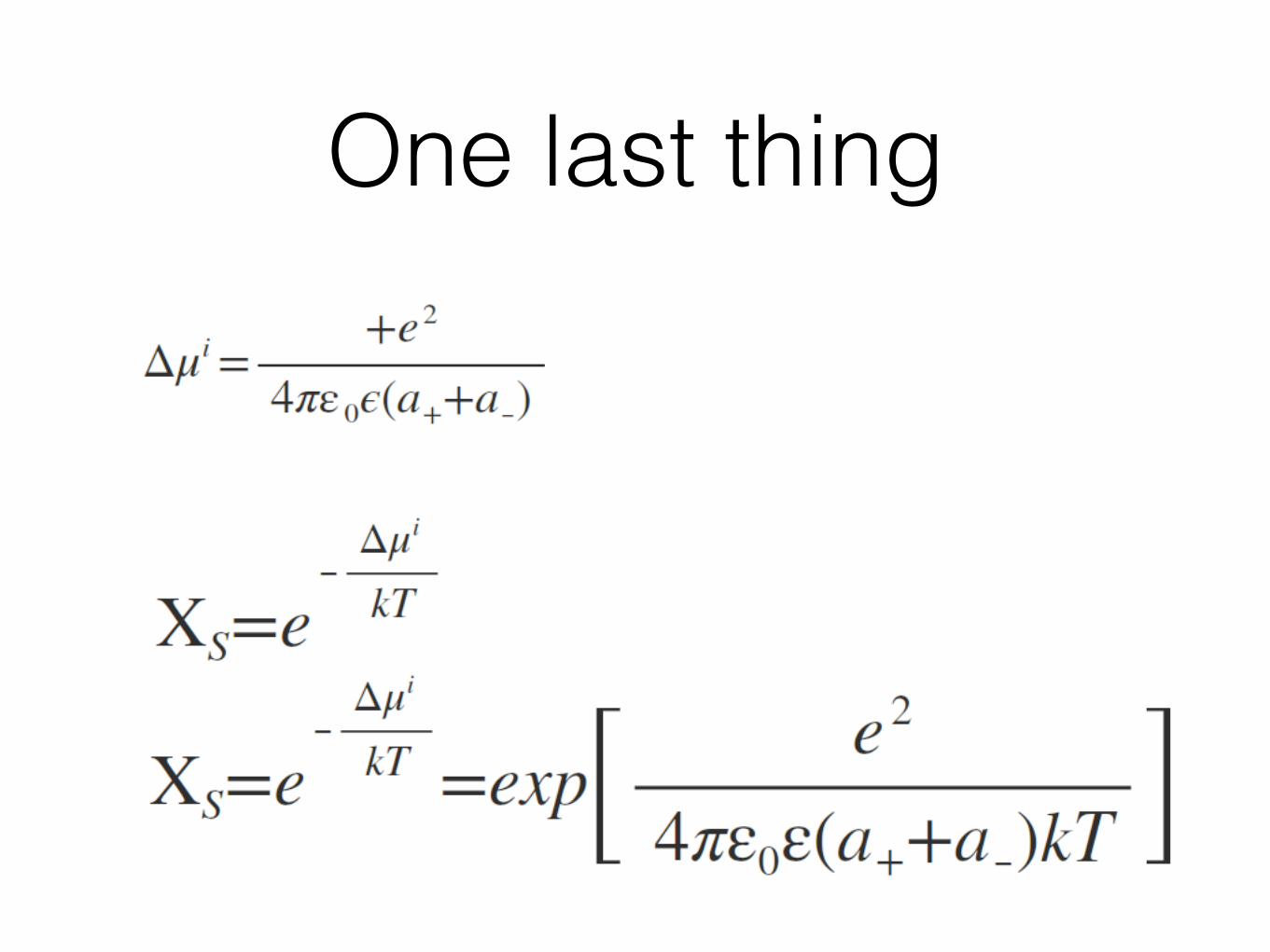
One last thing
problem in a way that takes the lattice energy into account: by splitting up the dissoci-ation process into two well-defined stages. The first is the dissociation of the solid intoisolated gaseous ions, and the second is the transfer of these ions into the solvent. In thisapproach (see, e.g., Dasent, 1970; Pass, 1973) the energy associated with the first stage issimply the positive lattice energy, while the second stage reduces this by the negativeBorn energies of transferring the ions from the gas phase (3 ¼ 1) into the solvent mediumof dielectric constant 3. However, for water, the theoretical Born energies turn out to bemuch too large, even larger than the lattice energies [compare Eq. (3.9) with Eq. (3.16)],
Methylformamide
WaterEthyleneglycol
Ethanolamine
Methanol
NaClGlycine
Methanol
0
Solu
bilit
y X
s (m
ole
fract
ion)
10–5
10–4
10–3
10–2
10–1
1200 100 40 30 20 1550
0.01 0.02 0.03 0.04 0.05 0.06 0.07
1/
Dielectric constant
Ethanol
EthanolButanol
Pentanol
Propanol
Butanol
Formamide
Formamide
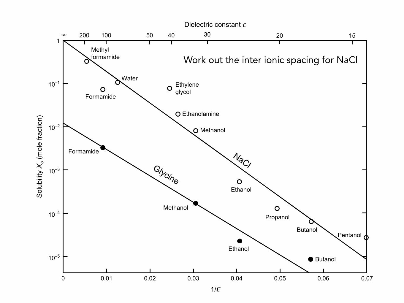
FIGURE 3.3 Solubilities of sodium chloride (NaCl $ NaþþCI#) and glycine (NH2CH2COOH $ NH3þCH2COO#) insolvents of different static dielectric constants 3 at 25$C. Solubility (in mole fraction units) is plotted as log Xs asa function of 1/3. For NaCl, the line passes through Xs¼ 1 at#3¼N, which from Eq. (3.18) suggests that the interactionof Naþþ CI#with these solvents is purely Coulombic. For glycine, the line tends to a finite value (Xs < 1) as 3 tends toinfinity, indicative of some additional type of solute-solute attraction # the van der Waals interaction (Chapter 6).Note that all the solvents are hydrogen-bonding liquids (Chapter 8). Non-hydrogen-bonding liquids are less effectiveas solvents for ionic species; for example, the solubility of NaCl in acetone (3 ¼ 20.7) is Xs ¼ 4 % 10#7 while that ofglycine in acetone is Xs ¼ 2% 10#6. Solubility data were taken from GMELINS Handbuch, Series 21, Vol. 7 for NaCl, andfrom the CRC Handbook of Chemistry and Physics for glycine.
64 INTERMOLECULAR AND SURFACE FORCES
Work out the inter ionic spacing for NaCl
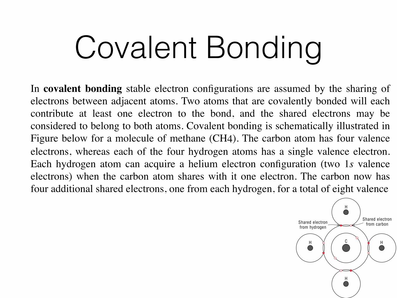
Covalent BondingIn covalent bonding stable electron configurations are assumed by the sharing of electrons between adjacent atoms. Two atoms that are covalently bonded will each contribute at least one electron to the bond, and the shared electrons may be considered to belong to both atoms. Covalent bonding is schematically illustrated in Figure below for a molecule of methane (CH4). The carbon atom has four valence electrons, whereas each of the four hydrogen atoms has a single valence electron. Each hydrogen atom can acquire a helium electron configuration (two 1s valence electrons) when the carbon atom shares with it one electron. The carbon now has four additional shared electrons, one from each hydrogen, for a total of eight valence
22 ● Chapter 2 / Atomic Structure and Interatomic Bonding
2.3 contains bonding energies and melting temperatures for several ionic materials.Ionic materials are characteristically hard and brittle and, furthermore, electricallyand thermally insulative. As discussed in subsequent chapters, these properties area direct consequence of electron configurations and/or the nature of the ionic bond.
COVALENT BONDINGIn covalent bonding stable electron configurations are assumed by the sharing ofelectrons between adjacent atoms. Two atoms that are covalently bonded will eachcontribute at least one electron to the bond, and the shared electrons may beconsidered to belong to both atoms. Covalent bonding is schematically illustratedin Figure 2.10 for a molecule of methane (CH4). The carbon atom has four valenceelectrons, whereas each of the four hydrogen atoms has a single valence electron.Each hydrogen atom can acquire a helium electron configuration (two 1s valenceelectrons) when the carbon atom shares with it one electron. The carbon now hasfour additional shared electrons, one from each hydrogen, for a total of eight valence
Table 2.3 Bonding Energies and Melting Temperatures forVarious Substances
Bonding Energy MeltingkJ/mol eV/Atom, Temperature
Bonding Type Substance (kcal/mol) Ion, Molecule (!C )
IonicNaCl 640 (153) 3.3 801MgO 1000 (239) 5.2 2800
CovalentSi 450 (108) 4.7 1410C (diamond) 713 (170) 7.4 !3550
Hg 68 (16) 0.7 "39
MetallicAl 324 (77) 3.4 660Fe 406 (97) 4.2 1538W 849 (203) 8.8 3410
van der WaalsAr 7.7 (1.8) 0.08 "189Cl2 31 (7.4) 0.32 "101
HydrogenNH3 35 (8.4) 0.36 "78H2O 51 (12.2) 0.52 0
Shared electronfrom hydrogen
Shared electronfrom carbon
HH C
H
H
FIGURE 2.10 Schematic representation ofcovalent bonding in a molecule of methane(CH4).
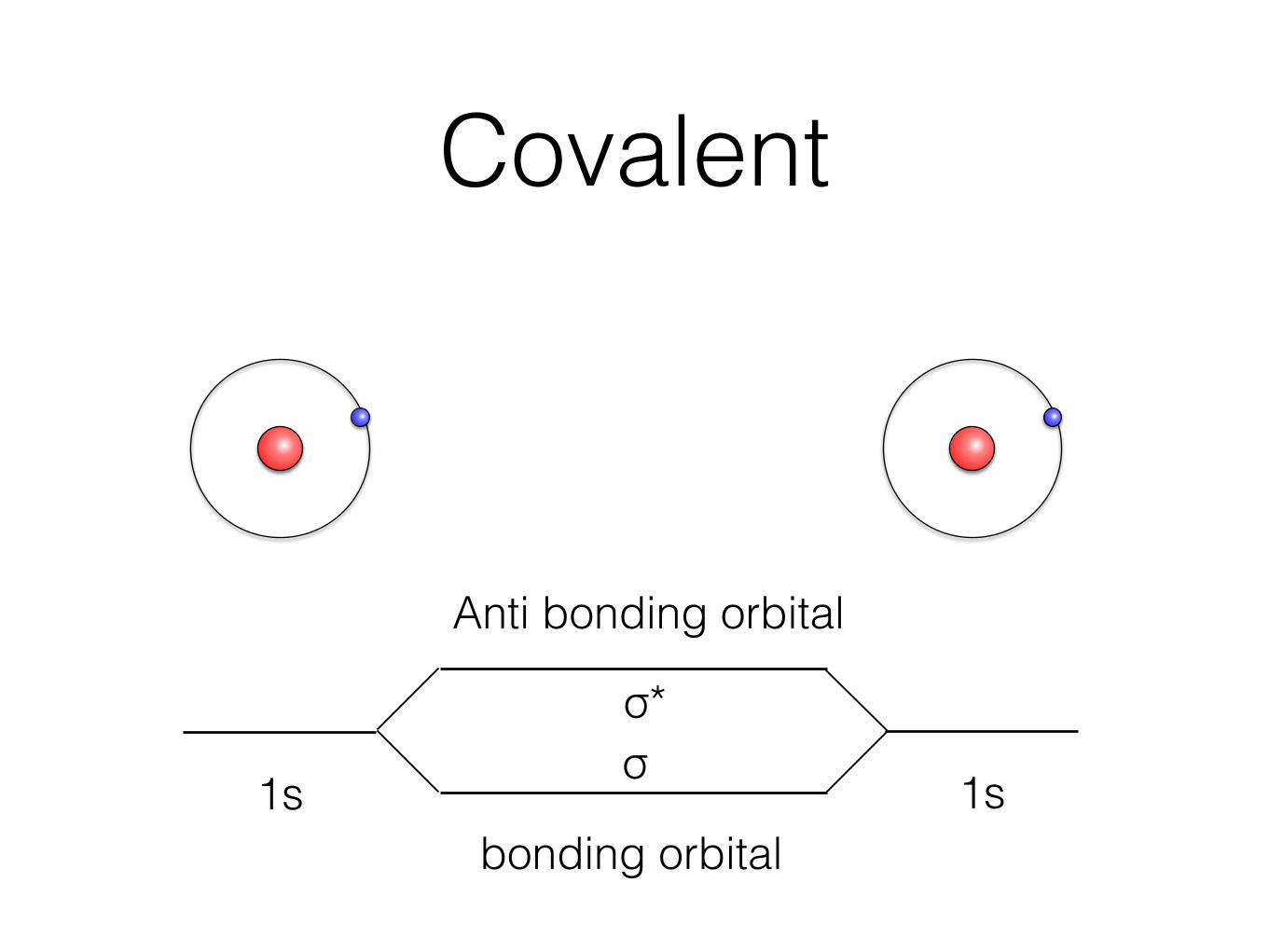
Covalent
1s 1s
Anti bonding orbital
bonding orbital
σσ*
Hydrogen
20 THE STRUCTURE OF MATERIALS
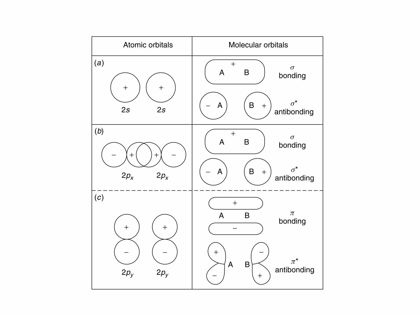
2s
2px 2px
2py 2py
+
2s
Atomic orbitals Molecular orbitals
+
− A
A B
B +
+
−
+ +
− −
−+ +
sbonding
A B+ s
bonding
pbonding
s*antibonding
− A
A B
B +
+
−
s*antibonding
p*antibonding
+
−
−
+A B
(a)
(b)
(c)
Figure 1.5 The shape of selected molecular orbitals formed from the overlap of two atomicorbitals. From K. M. Ralls, T. H. Courtney, and J. Wulff, Introduction to Materials Science andEngineering. Copyright © 1976 by John Wiley & Sons, Inc. This material is used by permissionof John Wiley & Sons, Inc.
Antibonding molecular orbital
Bonding molecular orbital
Molecule
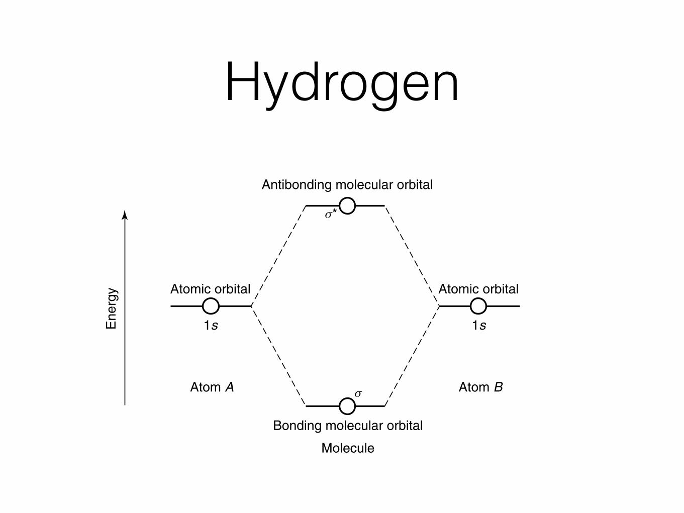
Atom A Atom B
1s 1s
Atomic orbital Atomic orbital
s*
s
Ene
rgy
Figure 1.6 Molecular orbital diagram for the hydrogen molecule, H2. Reprinted, by permission,from R. E. Dickerson, H. B. Gray, and G. P. Haight, Jr., Chemical Principles, 3rd ed., p. 446.Copyright © 1979 by Pearson Education, Inc.
20 THE STRUCTURE OF MATERIALS
2s
2px 2px
2py 2py
+
2s
Atomic orbitals Molecular orbitals
+
− A
A B
B +
+
−
+ +
− −
−+ +
sbonding
A B+ s
bonding
pbonding
s*antibonding
− A
A B
B +
+
−
s*antibonding
p*antibonding
+
−
−
+A B
(a)
(b)
(c)
Figure 1.5 The shape of selected molecular orbitals formed from the overlap of two atomicorbitals. From K. M. Ralls, T. H. Courtney, and J. Wulff, Introduction to Materials Science andEngineering. Copyright © 1976 by John Wiley & Sons, Inc. This material is used by permissionof John Wiley & Sons, Inc.
Antibonding molecular orbital
Bonding molecular orbital
Molecule
Atom A Atom B
1s 1s
Atomic orbital Atomic orbital
s*
s
Ene
rgy
Figure 1.6 Molecular orbital diagram for the hydrogen molecule, H2. Reprinted, by permission,from R. E. Dickerson, H. B. Gray, and G. P. Haight, Jr., Chemical Principles, 3rd ed., p. 446.Copyright © 1979 by Pearson Education, Inc.
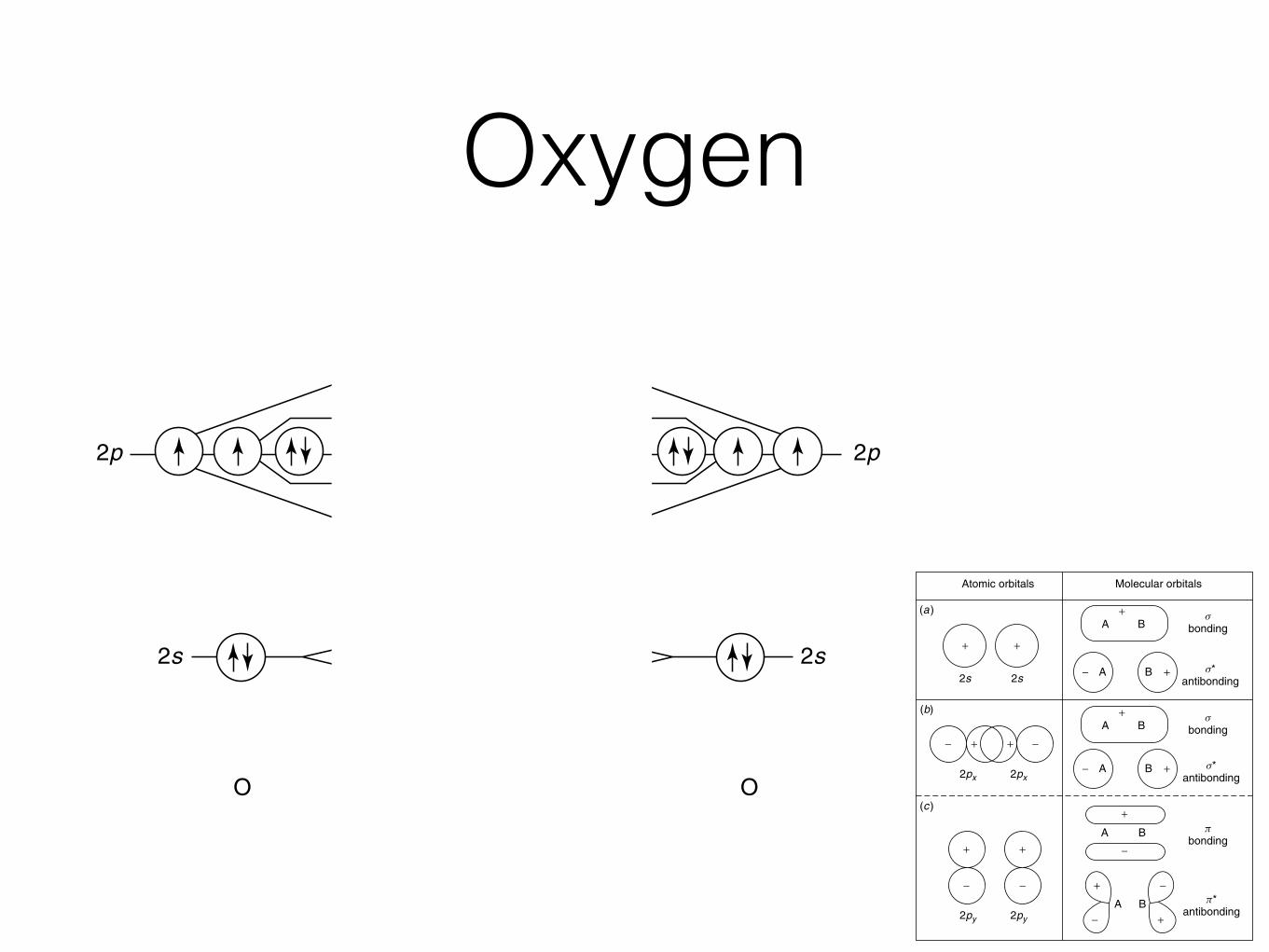
OxygenINTRODUCTION AND OBJECTIVES 21
2p 2p
2s
O O2 O
2s
p*2p
s*2p
s*2s
s2s
s2p
p2p
Figure 1.7 Molecular orbital diagram for molecular oxygen, O2. From K. M. Ralls, T. H.Courtney, and J. Wulff, Introduction to Materials Science and Engineering. Copyright © 1976by John Wiley & Sons, Inc. This material is used by permission of John Wiley & Sons, Inc.
Let us use molecular oxygen, O2, as an example. As shown in Figure 1.7, eachoxygen atom brings six outer-core electrons to the molecular orbitals. (Note that the1s orbitals are not involved in bonding, and are thus not shown. They could be shownon the diagram, but would be at a very low relative energy at the bottom of thediagram.) The 12 total electrons in the molecule are placed in the MOs from bottom totop; according to Hund’s rule, the last two electrons must be placed in separate π∗2porbitals before they can be paired.
The pairing of electrons in the MOs can manifest itself in certain physical prop-erties of the molecule. Paramagnetism results when there are unpaired electrons inthe molecular orbitals. Paramagnetic molecules magnetize in magnetic fields due tothe alignment of unpaired electrons. Diamagnetism occurs when there are all pairedelectrons in the MOs. We will revisit these properties in Chapter 6.
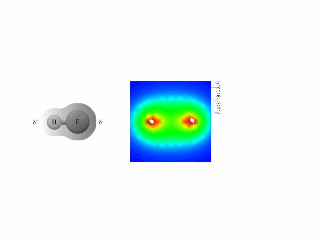
We can use molecular orbital theory to explain simple heteronuclear diatomicmolecules, as well. A molecule such as hydrogen fluoride, HF, has molecular orbitals,but we must remember that the atomic orbitals of the isolated atoms have much dif-ferent energies from each other to begin with. How do we know where these energiesare relative to one another? Look back at the ionization energies in Table 1.4, and yousee that the first ionization energy for hydrogen is 1310 kJ/mol, whereas for fluorine itis 1682 kJ/mol. This means that the outer-shell electrons have energies of −1310 (1selectron) and −1682 kJ/mol (2p electron), respectively. So, the electrons in fluorineare more stable (as we would expect for an atom with a much larger nucleus rela-tive to hydrogen), and we can construct a relative molecular energy diagram for HF(see Figure 1.8) This is a case where the electronegativity of the atoms is useful. Itqualitatively describes the relative energies of the atomic orbitals and the shape of theresulting MOs. The molecular energy level diagram for the general case of moleculeAB where B is more electronegative than A is shown in Figure 1.9, and the corre-sponding molecular orbitals are shown in Figure 1.10. In Figure 1.9, note how the Batomic orbitals are lower in energy than those of atom A. In Figure 1.10, note how thenumber of nodes increases from bonding to antibonding orbitals, and also note howthe electron probability is greatest around the more electronegative atom.
20 THE STRUCTURE OF MATERIALS
2s
2px 2px
2py 2py
+
2s
Atomic orbitals Molecular orbitals
+
− A
A B
B +
+
−
+ +
− −
−+ +
sbonding
A B+ s
bonding
pbonding
s*antibonding
− A
A B
B +
+
−
s*antibonding
p*antibonding
+
−
−
+A B
(a)
(b)
(c)
Figure 1.5 The shape of selected molecular orbitals formed from the overlap of two atomicorbitals. From K. M. Ralls, T. H. Courtney, and J. Wulff, Introduction to Materials Science andEngineering. Copyright © 1976 by John Wiley & Sons, Inc. This material is used by permissionof John Wiley & Sons, Inc.
Antibonding molecular orbital
Bonding molecular orbital
Molecule
Atom A Atom B
1s 1s
Atomic orbital Atomic orbital
s*
s
Ene
rgy
Figure 1.6 Molecular orbital diagram for the hydrogen molecule, H2. Reprinted, by permission,from R. E. Dickerson, H. B. Gray, and G. P. Haight, Jr., Chemical Principles, 3rd ed., p. 446.Copyright © 1979 by Pearson Education, Inc.
Question
• Can you do the same for nitrogen

Take Home
• Ionic strong, non direction
• Covalent can be strong but are directional

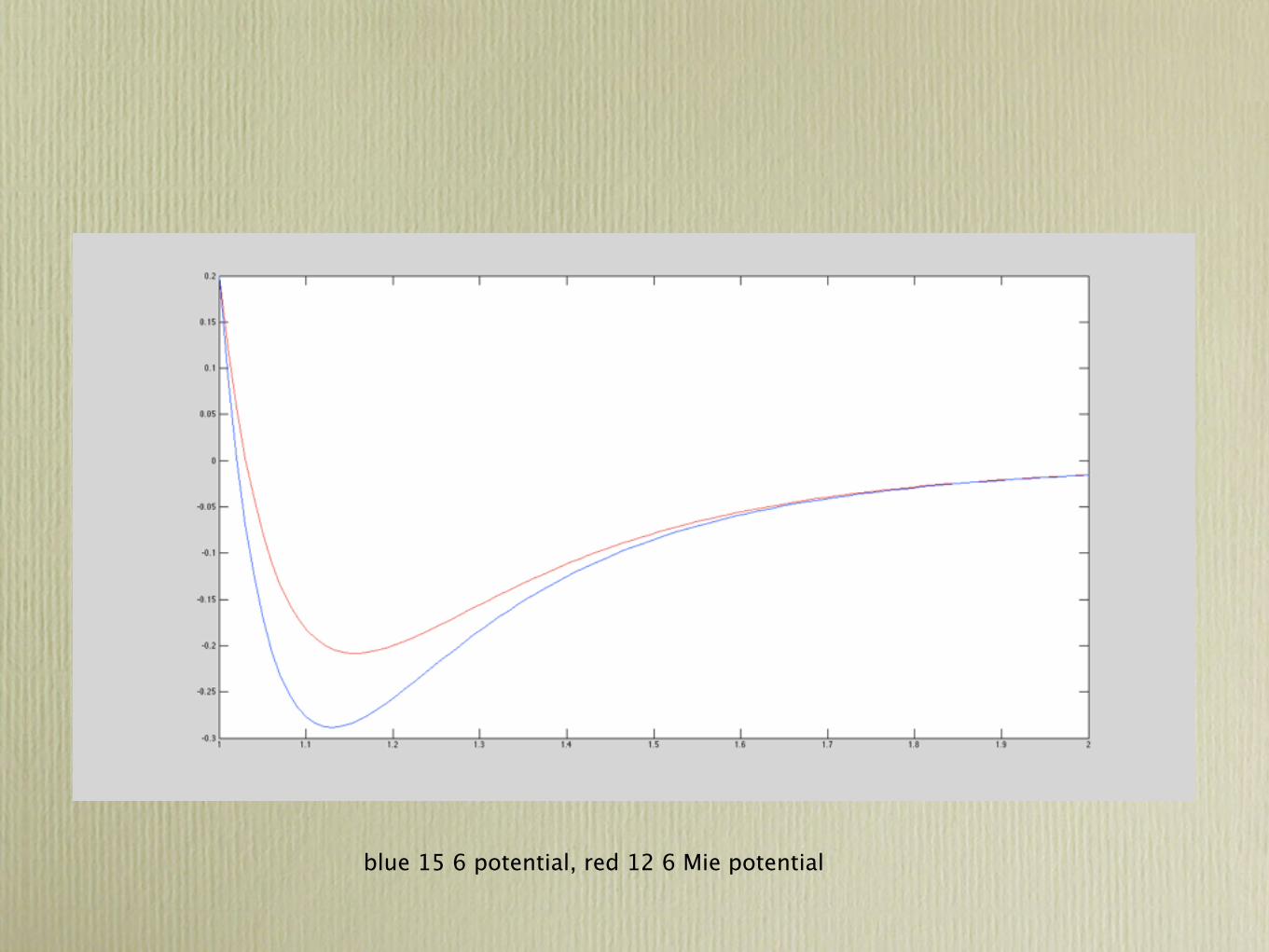
Mie Potential
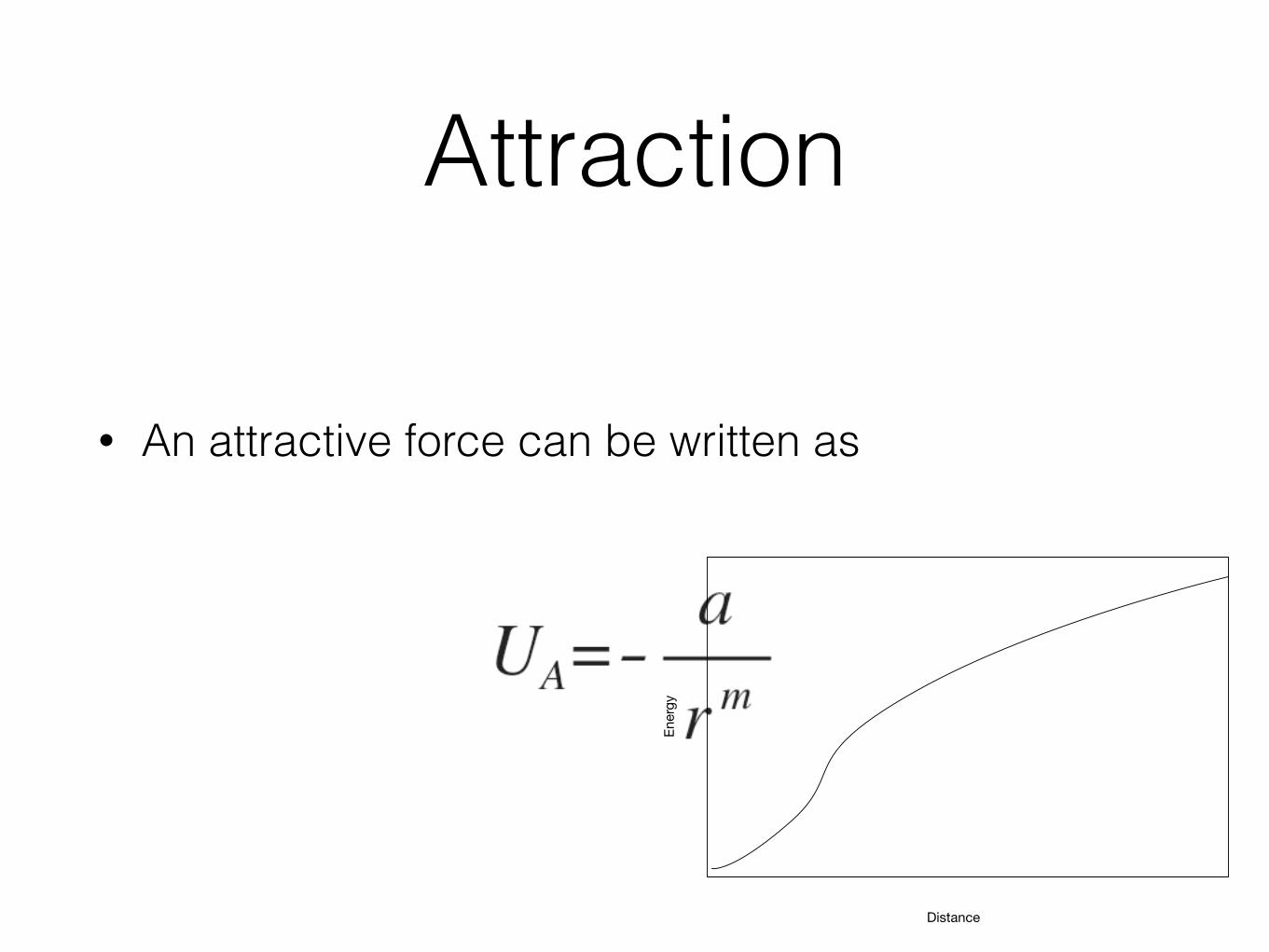
Attraction
• An attractive force can be written as
Distance
Energy
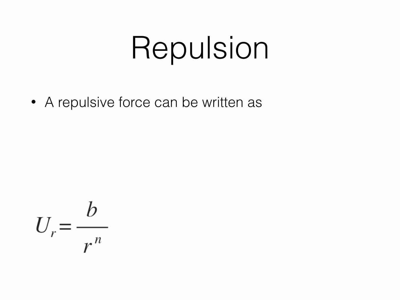
Repulsion• A repulsive force can be written as
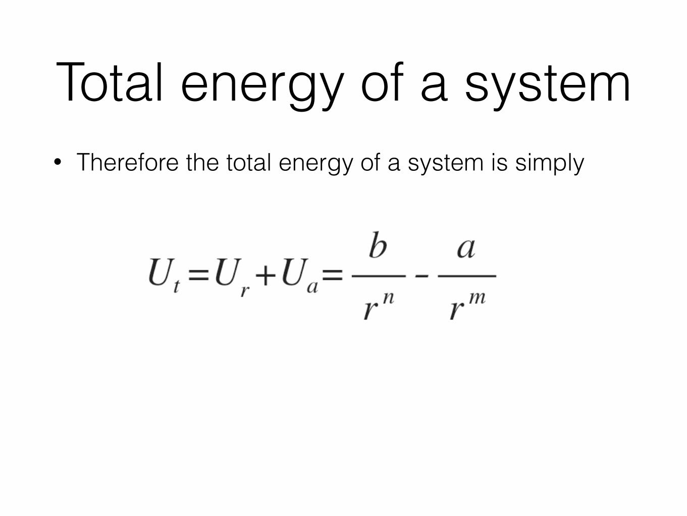
Total energy of a system• Therefore the total energy of a system is simply
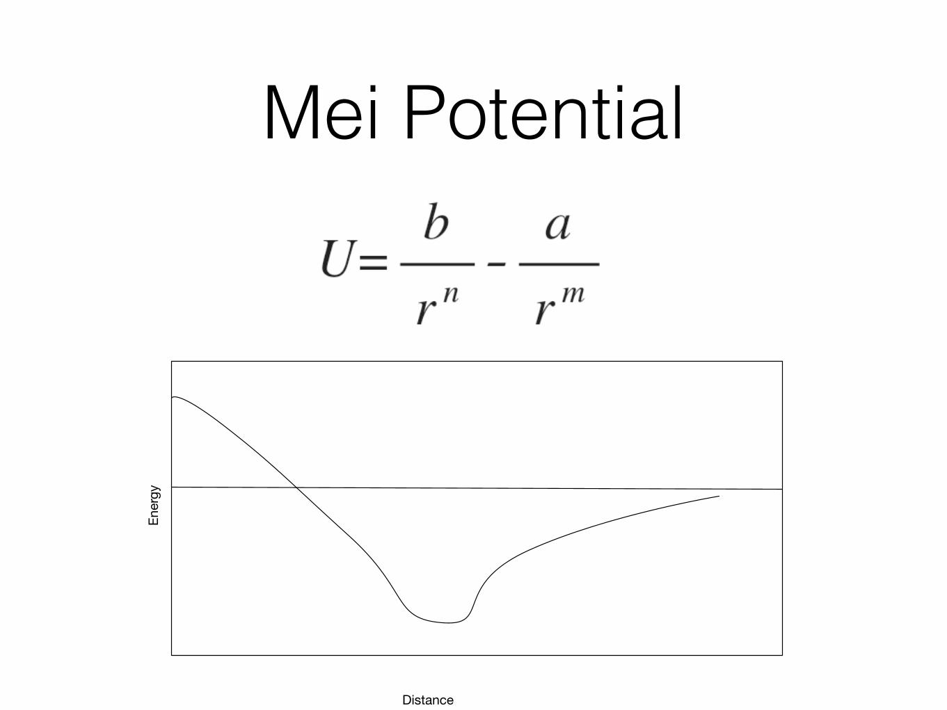
Mei Potential
Distance
Energy
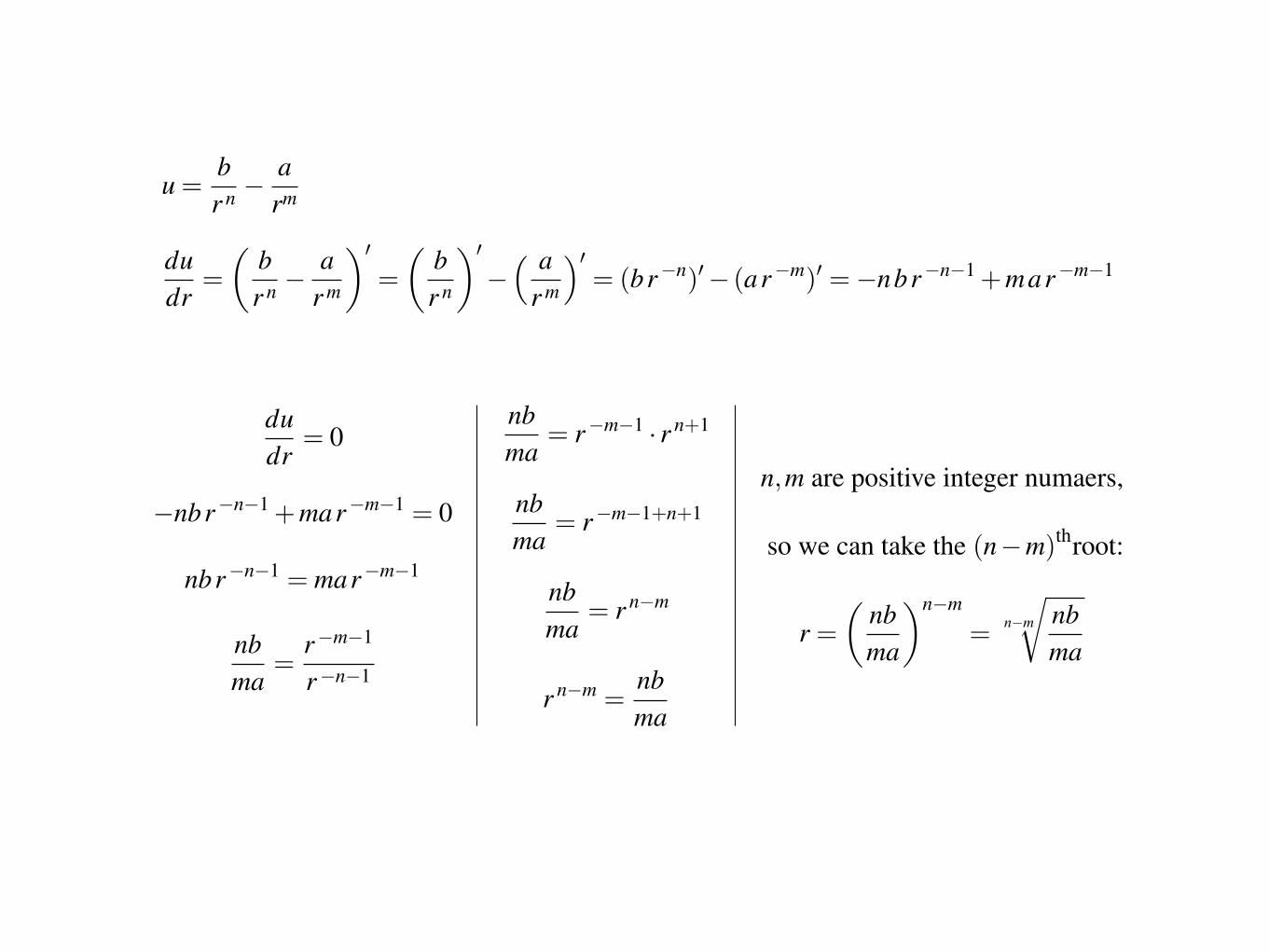
u =br n �
arm
dudr
=
✓br n �
ar m
◆0=
✓br n
◆0�⇣ a
r m
⌘0= (br�n)0 � (ar�m)0 =�nbr�n�1 +mar�m�1
dudr
= 0
�nbr�n�1 +mar�m�1 = 0
nbr�n�1 = mar�m�1
nbma
=r�m�1
r�n�1
nbma
= r�m�1 · r n+1
nbma
= r�m�1+n+1
nbma
= r n�m
r n�m =nbma
n,m are positive integer numaers,
so we can take the (n�m)th
root:
r =✓
nbma
◆n�m
=n�m
rnbma
1
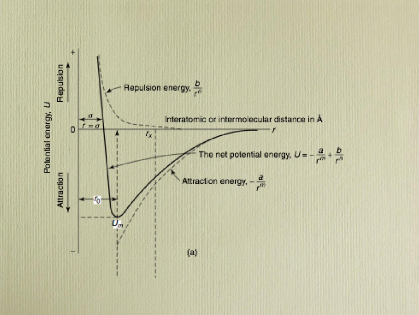
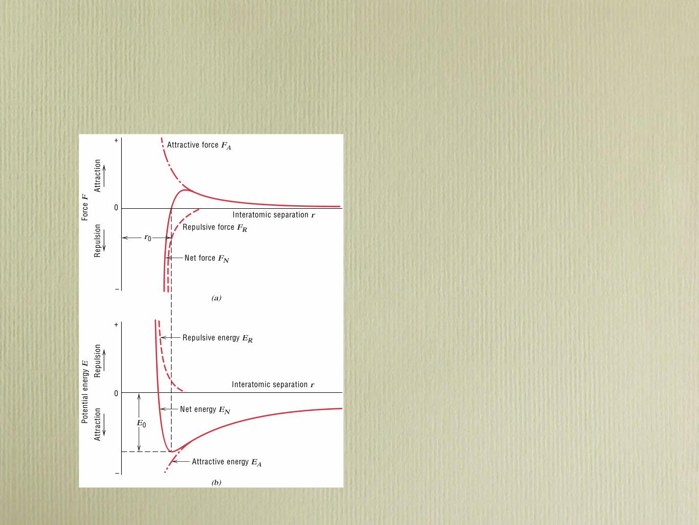
2.5 Bonding Forces and Energies ● 19
which is also a function of the interatomic separation, as also plotted in Figure2.8a. When FA and FR balance, or become equal, there is no net force; that is,
FA ! FR " 0 (2.3)
Then a state of equilibriumexists.The centers of the two atoms will remain separatedby the equilibrium spacing r0 , as indicated in Figure 2.8a. For many atoms, r0 isapproximately 0.3 nm (3 A). Once in this position, the two atoms will counteractany attempt to separate them by an attractive force, or to push them together bya repulsive action.
Sometimes it is more convenient to work with the potential energies betweentwo atoms instead of forces.Mathematically, energy (E) and force (F) are related as
E " ! F dr (2.4)
Or, for atomic systems,
EN " !r
!FN dr (2.5)
" !r
!FA dr ! !r
!FR dr (2.6)
" EA ! ER (2.7)
in which EN , EA , and ER are respectively the net, attractive, and repulsive energiesfor two isolated and adjacent atoms.
+
(a)
(b)
Interatomic separation r
Interatomic separation r
Repulsive force FR
Attractive force FA
Net force FN
Attr
actio
nR
epul
sion
Forc
e F
Repulsive energy ER
Attractive energy EA
Net energy EN
+
0
0
Attr
actio
nR
epul
sion
Pote
ntia
l ene
rgy E
r0
E0
FIGURE 2.8 (a) Thedependence of repulsive,attractive, and net forces oninteratomic separation fortwo isolated atoms. (b) Thedependence of repulsive,attractive, and net potentialenergies on interatomicseparation for two isolatedatoms.
blue 15 6 potential, red 12 6 Mie potential
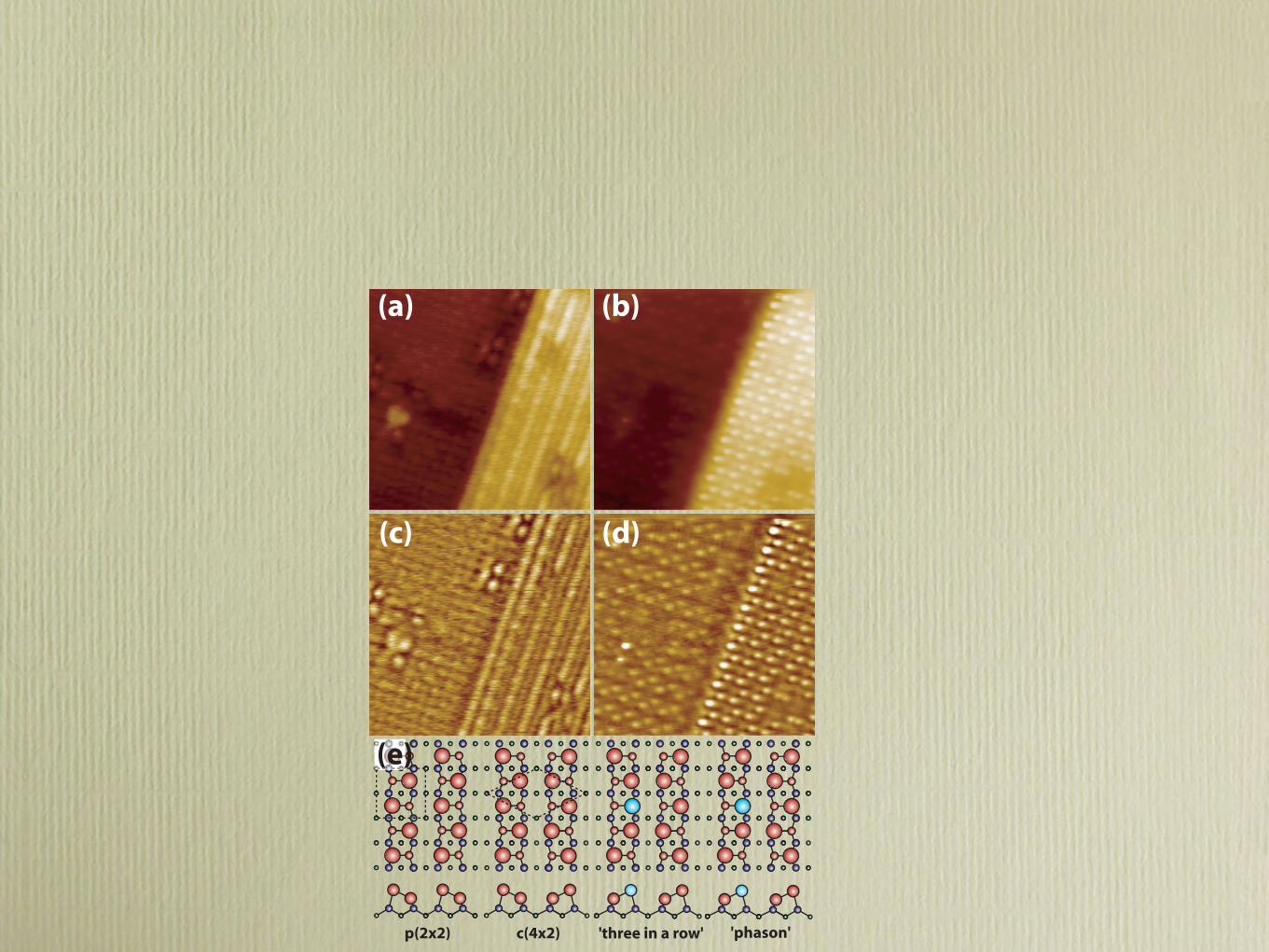
A. SWEETMAN et al. PHYSICAL REVIEW B 84, 085426 (2011)
p(2x2) 'phason'c(4x2) 'three in a row'
(c) (d)
(b)(a)
(e)
FIG. 1. (Color online) (a) Constant ⟨It ⟩ dSTM image of step edgeon Si(100) at 5 K. Vgap = +2 V; ⟨It ⟩ = 100 pA; A0 = 250 pm.(b) Constant !f FM-AFM image of the same region!f = −17.6 Hz; A0 = 250 pm; Vgap = 0 V. (c) and(d) High pass filtered images of (a) and (b) respec-tively. The dSTM image shows significant nonlocal contri-butions (see main text). Zero-bias FM-AFM imaging showsthe buckled c(4 × 2)/p(2 × 2) reconstructions on both terraces.(e) Schematics showing the p(2 × 2) and c(4 × 2) reconstructions. Asingle dimer flip from the c(4 × 2) would result in a “three-in-a-row”structure (never observed experimentally). A phason (phase defect)results in a switch between in-phase [c(4 × 2)] and out-of-phase[p(2 × 2)] buckling.
operating in ultrahigh vacuum (UHV) (base pressure 5 ×10⁻¹¹ mbar or better), in a LHe/LN2 bath cryostat (sampletemperature approximately 5 K for cooling with LHe, 77 Kwith LN2). We used boron-doped (1 m"cm) Si(100) surfaceswhich were prepared in UHV by standard methods (flashheating to ∼1200 ◦C; rapid cooling to ∼900 ◦C; slow coolingto room temperature) before transfer into the low-temperaturecryostat. After preparation, we checked the Si(100) surfacereconstruction by conventional STM using a qPlus sensorbefore beginning FM-AFM experiments. We used commercialqPlus sensors (Omicron) with an electrochemically etchedtungsten wire attached to one tine of the tuning fork. Thesewere introduced into the scan head without further preparation(e.g., e-beam heating or argon sputtering). Calibration of the
quality factor and stiffness are described in detail elsewhere.28
Briefly, we recorded Q factors of between 1000 and 50 000at 5 K with resonance frequencies of between 22 and 25 kHz,and tuning fork stiffness of k = 2600 N/m (±400 N/m).28
The sensors were prepared using standard STM techniques(e.g., voltage pulsing, controlled tip crashes) until atomicresolution was obtained. We then performed dynamic STM(dSTM) (i.e., tunnel-current-based feedback with an oscil-lating tip) and transferred to constant !f (i.e., FM-AFM)feedback and subsequently reduced the tip bias to 0 V. Wewould then increase the frequency shift set point until we beganto observe atomic resolution. In some cases we immediatelyobtained atomic resolution after transferring from dSTM;in other cases it was necessary to perform small controlledcontacts with the surface to alter the tip state. As a consequenceof our tip preparation techniques (and evidence from scanningelectron microscope measurements on similarly prepared STMtips28) we expect the apex of the tip to be silicon rather thantungsten terminated. The reduction of the tip bias to 0 V isessential both in order to remove the possibility of electroniccrosstalk from the It channel30 and, critically, to also eliminatethe effect of tunneling electrons. As a consequence, we donot null out any contact potential difference (CPD) betweentip and surface, and as such a large electrostatic backgroundmay be present. Nonetheless, we routinely observed atomicresolution even with relatively blunt tips (e.g., tips thatexperienced surface indentations in excess of 1000 nm couldstill produce atomic resolution), most likely because operatingwith small oscillation amplitudes increases our sensitivity tothe short-range chemical force.31–33
B. Simulations
We simulated the interaction between the silicon surfaceand a silicon tip cluster by ab initio density functionaltheory (DFT) as implemented in the SIESTA code.35 Two tipclusters were used, a standard Si(111)-type tip and a largerdimer-terminated cluster, as described elsewhere.28 We used adouble-zeta polarized basis set giving 13 orbitals to describethe valence electrons on every silicon atom. Calculationswere performed with the generalized gradient approximation(GGA) Perdew-Burke-Ernzerhof (PBE) density functional andnorm-conserving pseudopotentials. Typically, atomic relax-ation was considered complete when forces on atoms werenot larger than 0.01 eV/A.
In all simulations a 6-layer slab model was used with16 surface dimers arranged as 2 rows, each 8 dimers in length.Hydrogen atoms were used to terminate the Si bonds on thelower side of the slab and were kept fixed, along with thebottom two layers of silicon, to simulate the missing bulk.We used a large slab size to provide reasonable isolation of thetarget atoms in order to reduce finite-size effects due to periodicboundary conditions. Atoms are only manipulated within asingle row, such that there is always a single unaffected dimerrow between the manipulated row and its periodically repeatedcounterparts. In addition, the length of each row was chosen toreduce any effect due to long-range surface relaxations alongthe rows. For example, when modeling a phason pair (twoadjacent phasons, four dimers in length), four other dimers,in a standard c(4 × 2) buckling configuration, separate the
085426-2
MANIPULATING Si(100) AT 5 K USING qPlus . . . PHYSICAL REVIEW B 84, 085426 (2011)
-140
-120
-100
-80
-60
-40
-20
∆f(H
z)
Flip type i App. Flip type i Ret. up atom App. up atom Ret.
(a)
-140
-120
-100
-80
-60
-40
-20
∆f(H
z)
Fail flip type i App. Fail flip type i Ret. up atom App. up atom Ret.
(b)
-140
-120
-100
-80
-60
-40
-20
-2.5 -2.0 -1.5 -1.0 -0.5 0.00 0.5Z (Å)
∆f(H
z)
Fail flip type ii App. Fail flip type ii Ret. up atom App. up atom Ret.
(c)
-2.0 -1.5 -1.0 -0.5 0.0-65
-60
-55
-50
-45
-40
-35
-30
∆f(H
z)
Z (Å)
Flip type ii App. Flip type ii Ret. up atom App. up atom Ret.
(d)
-2.5 -2.0 -1.5 -1.0 -0.5 0.00 0.5Z (Å)
-2.5 -2.0 -1.5 -1.0 -0.5 0.00 0.5Z (Å)
α
β
γ
α α
α
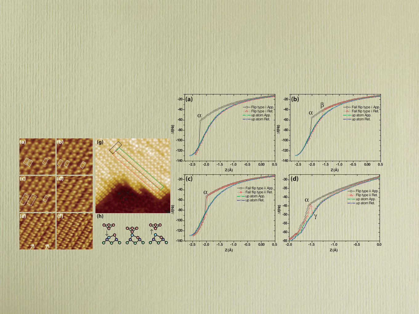
FIG. 8. (Color online) Representative examples of !f (z) “signatures.” (a) to (c) were acquired using the same tip apex (A0 = 50 pm). (d)was acquired using a different tip apex and different parameters (A0 = 250 pm) as this type of event was comparatively rare. On each graph a!f (z) curve taken over an “up” atom with the same tip is plotted to aid comparison with the retract !f (z) curves. (a) Successful flip type (i),showing a smooth increase followed by a sudden discontinuity (α) and subsequent retract along a different path. The retract curve exhibits astrong similarity to the !f (z) curve taken over an “up” atom. (b) Unsuccessful flip type (i). Similar behavior as shown in (a) except that onthe retract a sudden jump back onto the approach curve is detected (β), indicating that the atom under the tip has dropped back into a “down”state. (c) Unsuccessful flip type (ii). In this instance the jump on retract is in almost the same position as the initial jump, resulting in very littlehysteresis in the !f (z) curve. (d) Successful flip type (ii) taken from a different data set with a different long-range !f (z) behavior. Here itappears that the flip has failed as the retract follows the same path as approach, but then suddenly jumps down onto the “up” atom curve (γ ).
the same z position) such that the !f curve on the retractfollows the same path as the approach. In these cases there isonly a very small amount of hysteresis between the two paths.A simple interpretation of these events is that the down atom ispulled up, but is not stable without the presence of the tip, andas the tip leaves the surface the dimer simply drops back intoits original configuration. This suggests that small variations inthe potential energy surface may sometimes enable the systemto go back from the three-in-a-row configuration to c(4 × 2)even with the tip relatively close to the surface. In this instancethe results closely resemble a simulated failed flip using alaterally displaced Si(111)-type tip [Fig. 7(a)].
4. Successful flip type (ii)
Very rarely we would observe a jump on the approach andretract [as for a failed type (ii)], but subsequently during theretract we then see a further jump to a higher !f value andsubsequent different path during the rest of the retract. In theseevents it appears that the dimer flips, then drops back into itsoriginal configuration as the tip retracts, but then flips againand stays in the up position as the tip retracts. The tip-surfacedynamics in these cases present a particular challenge as the
dimer appears to be flipping after the peak force has beenreached and the tip is already retracting, suggestive of complexrelaxations at the tip-surface interface.
C. Long-range relaxations during phason manipulation
Although we have demonstrated that the motion andpositioning of phasons can be controlled with atomic precisionby FM-AFM spectroscopy, we nonetheless also observeexamples of unexpected long-range relaxations that hint atfurther complex intra-row coupling. We regularly observedtwo or more dimers flipping when we attempted to form “three(or more) in a row” structures, which, while not predicted inour simulations, may be expected if the surface is attemptingto release a large quantity of locally induced strain. In addition,however, we also see long-range relaxations in locations wherewe would expect a single dimer flip to occur. What is strikingin these examples is that the expected “target” structuresare not only stable, but have been successfully formed inother regions during FM-AFM manipulation experiments.Consequently, it appears that variations in surface stabilitymay affect not only our ability to create phason pairs, but alsorestrict our ability to maintain atomically precise control of
085426-7
MANIPULATING Si(100) AT 5 K USING qPlus . . . PHYSICAL REVIEW B 84, 085426 (2011)
structure from the repeat of the phason unit. Because of thecell sizes used, only the ! point was employed in sampling theBrillouin zone in all of our simulations.
To estimate the energy barriers between different configu-rations we performed nudged elastic band (NEB) calculations,using SIESTA to calculate the total energies. In our NEBcalculations we modeled the evolution of the energy bandcorresponding to the minimum energy path between thec(4 × 2) and phason pair structures in the presence of asilicon tip cluster. The NEB method allowed us to calculatethe dimer atom positions and energy barriers associated withthe minimum energy pathway between two states. Initially, thestart and end points on the band were relaxed and the atomicpositions along the band were obtained by a linear interpolationwith 17 images in each band. For the data presented in thispaper the band was then relaxed until the energies of the imagesvaried by less than 0.01 eV and the force less than 0.1 eV/A.
III. RESULTS
Our results are divided into two broad categories. First,we discuss imaging of the Si(100) surface and variation in thesurface stability observed during scanning, comparing the datato simulated variations in surface stability. Second, we investi-gate the variations in tip-surface dynamics during site-specificatomic switching events induced by "f (z) spectroscopy andattempt to elucidate the dynamics by comparison to simulatedforce spectroscopy.
A. Local variation in surface stability during scanning
During our dSTM experiments we observed a stronginfluence of tip bias and tunnel current set point on the imagingprocess, as previously reported. The observed surface structurecan change as a result of tunnel current injection, tunnelinginto nonlocalized surface and bulk states and charging atdefects.20–22,24,36,37 However, once we transition to zero-biasFM-AFM we always observe buckled dimers in the p(2 ×2)/c(4 × 2) configuration on both terraces (Fig. 1 shows atypical transition). In this instance we note the dSTM imageshows significant influence from the tip state as the upper andlower terraces show different contrast [p(2 × 1) on the lowerterrace and rows on the upper terrace]. Given the relativelyhigh bias applied during the dSTM imaging (+2 V), there arelikely to be significant contributions from the bulk-like statesof the surface and tip, and elucidating the origin of this contrastis beyond the scope of this paper. Importantly, this influence isnot apparent in the FM-AFM image, highlighting the differentorigin of the contrast in each imaging mode.
It is well known that the buckling of the silicon dimerscan be “pinned,” even at room temperature, by features suchas defects, adsorbed molecules, or step edges due to theireffect on the local strain along the surface. Consequently, thebarrier for dimer flipping exhibits strong local variation.29,38,39
Similarly, we found local variations in the propensity fordimers to flip under the influence of the tip at low temperatures.This is clearly demonstrated in Fig. 2 (see also movie S130),which shows the transition from the buckled structure to theapparent symmetric p(2 × 1) periodicity as the "f set pointis increased.23 In particular in Fig. 2(f) the apparent p(2 × 1)
(a) (b)
(d)
(e) (f)
(c)
(g)
(h)
FIG. 2. (Color online) Scan-induced phason manipulation andc(4 × 2)-to-p(2 × 1) transition. (a) FM-AFM image showing anunperturbed buckled surface structure and three “native” phasondefects (highlighted). "f = −26 Hz; A0 = 100 pm; Vgap = 0 V.(b) "f = −27 Hz. At higher set points we observe scan-inducedphason motion, as previously reported (Ref. 28). (c) "f = −28 Hz.At still higher set points the position of some of the phasons becomesdifficult to identify (larger highlighted regions). (d) "f = −29 Hz.“Intermittent” imaging. It is now likely that dimers are being flippedfrom the buckled state in addition to scan-induced phason motion.Clear “slicing” is evident in a number of rows. (e) "f = −31 Hz.At high set points some rows now show the apparent p(2 × 1)phase while some remain buckled (indicated by white arrows). (f)"f = −34 Hz. The highest set point at which we could reliablyimage with this tip—see main text for details. (g) Scan taken with adifferent tip at 77 K and a small bias voltage illustrating long-rangedifferences in dimer stability. "f = −40 Hz; A0 =100 pm; Vgap ∼10 mV. A boron ad-dimer defect (Ref. 34) (black box) appears toreduce the barrier for dimer flipping in the row highlighted by thegreen box. An adjacent row (red box) images as a stable buckledstructure. The apparent effect of the defect on dimer stability extendsover almost 30 dimers. Note that due to the small bias we cannotexclude tunnel-current-induced flipping in this instance (⟨It ⟩ duringimaging ∼2 pA). (h) Cartoon representation of tip-induced dimerflipping.
phase is clear in a number of rows. Nonetheless, two rows stillshow a buckled structure, indicating that even under the sameimaging conditions some dimers are less likely to be perturbedby the tip-sample interaction. We note that the rows remainingbuckled have an asymmetric appearance, most likely due to anasymmetric tip apex. Figure 2(g) demonstrates a clear exampleof the nonlocal effect that defects can exert on dimer stability.A previous study reported that strain at step edges resulted ina lowering of the surface stability on the lower terrace andan apparent p(2 × 1) periodicity during FM-AFM imaging.40
We, however, always observed buckling on both terraces at lowset point, with no apparent preference for scan-induced phasonmotion (see below) on either terrace. This variance may bedue to our elimination of the effect of tunneling electrons, orpossibly variation in defect density close to the scan region.
When the scan-induced p(2 × 1) periodicity is observedwe note that determining the actual structure of the surface(at a given instant) is likely to be nontrivial. This is primarily
085426-3
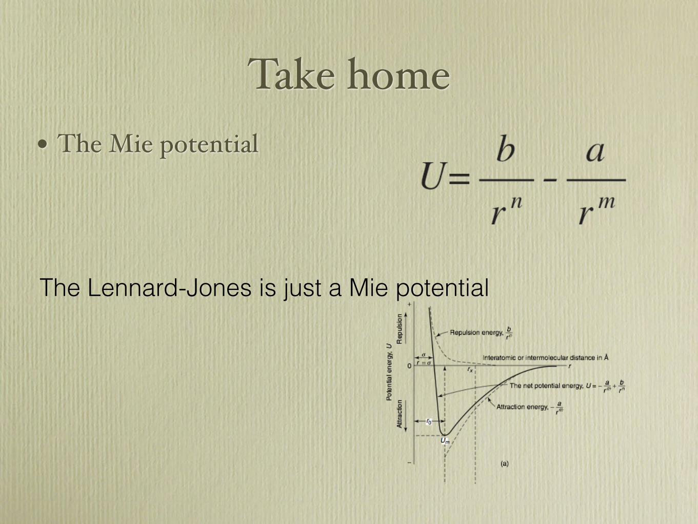
Take home• The Mie potential
The Lennard-Jones is just a Mie potential