Embed Size (px)
Citation preview
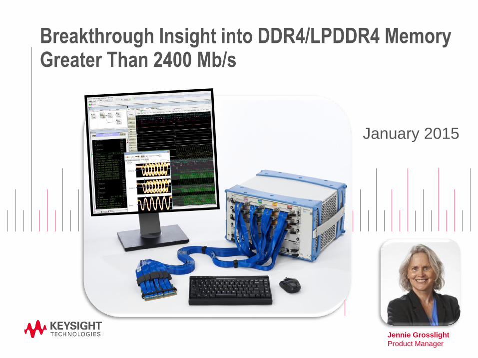
Breakthrough Insight into DDR4/LPDDR4 Memory Greater Than 2400 Mb/s
Jennie Grosslight
Product Manager
January 2015
Page 2
Agenda
– Overview
• Benefits and challenges for DDR4 and LPDDR4 >2400Mb/s
• Breakthrough Insight Gained from Logic Analyzer
– Techniques to address debug and validation challenges
• DDR Eye Scan insight
• DDR4 >3.1 Gb/s DIMM system
- Tuning tool
- Waveforms and Burst Trigger
- View Initialization
- Follow the initialization signal flow
- Compliance and Performance Tools
– Successful logic analyzer probing techniques for higher data rates
– DDR Solution Overview, Recommendations, & Q&A
Page
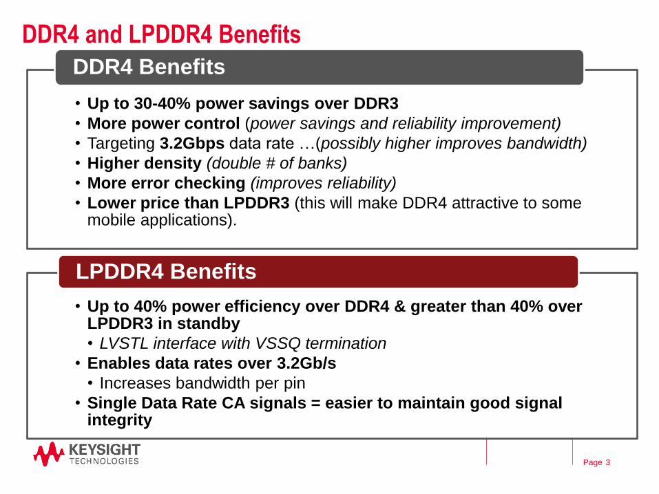
DDR4 and LPDDR4 Benefits
• Up to 30-40% power savings over DDR3
• More power control (power savings and reliability improvement)
• Targeting 3.2Gbps data rate …(possibly higher improves bandwidth)
• Higher density (double # of banks)
• More error checking (improves reliability)
• Lower price than LPDDR3 (this will make DDR4 attractive to some mobile applications).
DDR4 Benefits
• Up to 40% power efficiency over DDR4 & greater than 40% over LPDDR3 in standby
• LVSTL interface with VSSQ termination
• Enables data rates over 3.2Gb/s
• Increases bandwidth per pin
• Single Data Rate CA signals = easier to maintain good signal integrity
LPDDR4 Benefits
3
Page
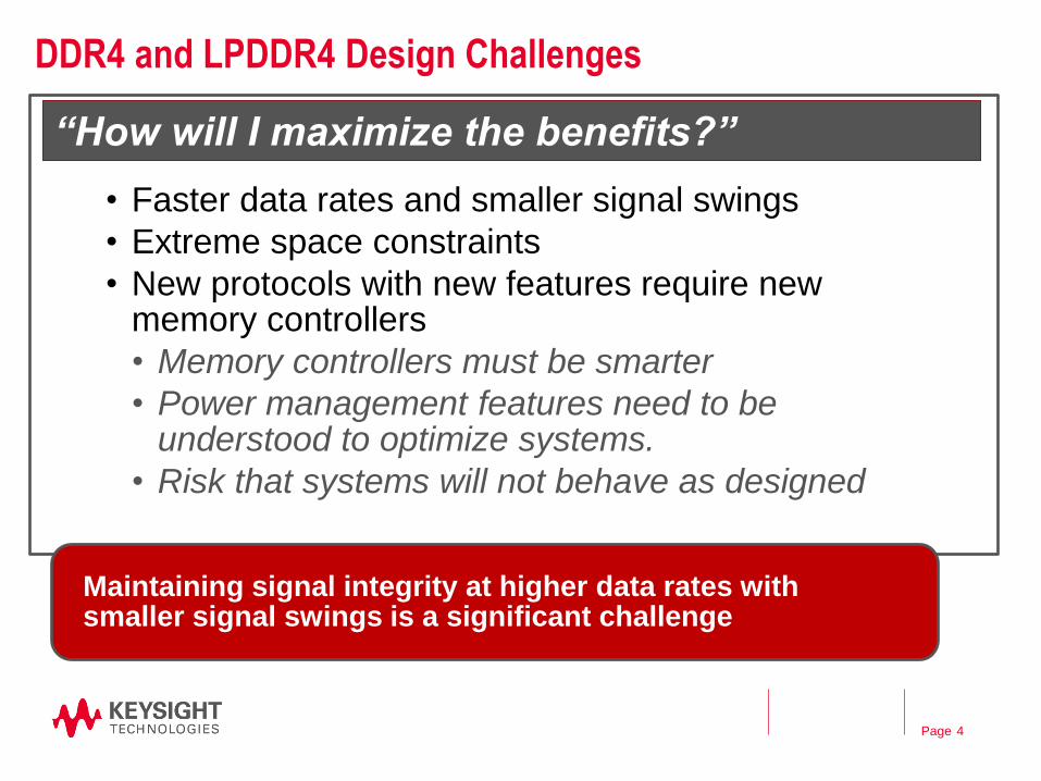
DDR4 and LPDDR4 Design Challenges
• Faster data rates and smaller signal swings
• Extreme space constraints
• New protocols with new features require new memory controllers
• Memory controllers must be smarter
• Power management features need to be understood to optimize systems.
• Risk that systems will not behave as designed
Maintaining signal integrity at higher data rates with smaller signal swings is a significant challenge
“How will I maximize the benefits?”
4
Page
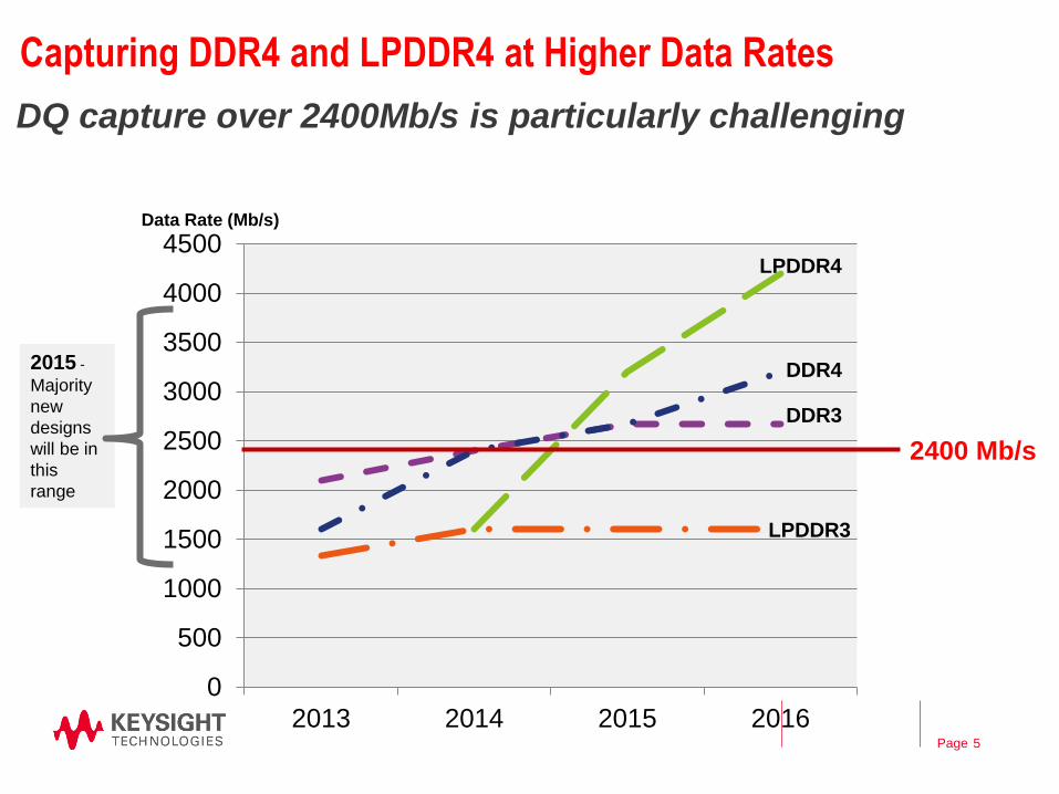
Capturing DDR4 and LPDDR4 at Higher Data Rates
Data Rate (Mb/s)
2015 -
Majority
new
designs
will be in
this
range
DQ capture over 2400Mb/s is particularly challenging
0
500
1000
1500
2000
2500
3000
3500
4000
4500
2013 2014 2015 2016
LPDDR4
LPDDR3
DDR4
DDR3
5
2400 Mb/s
Page
2013 2015
Dat
a R
ate
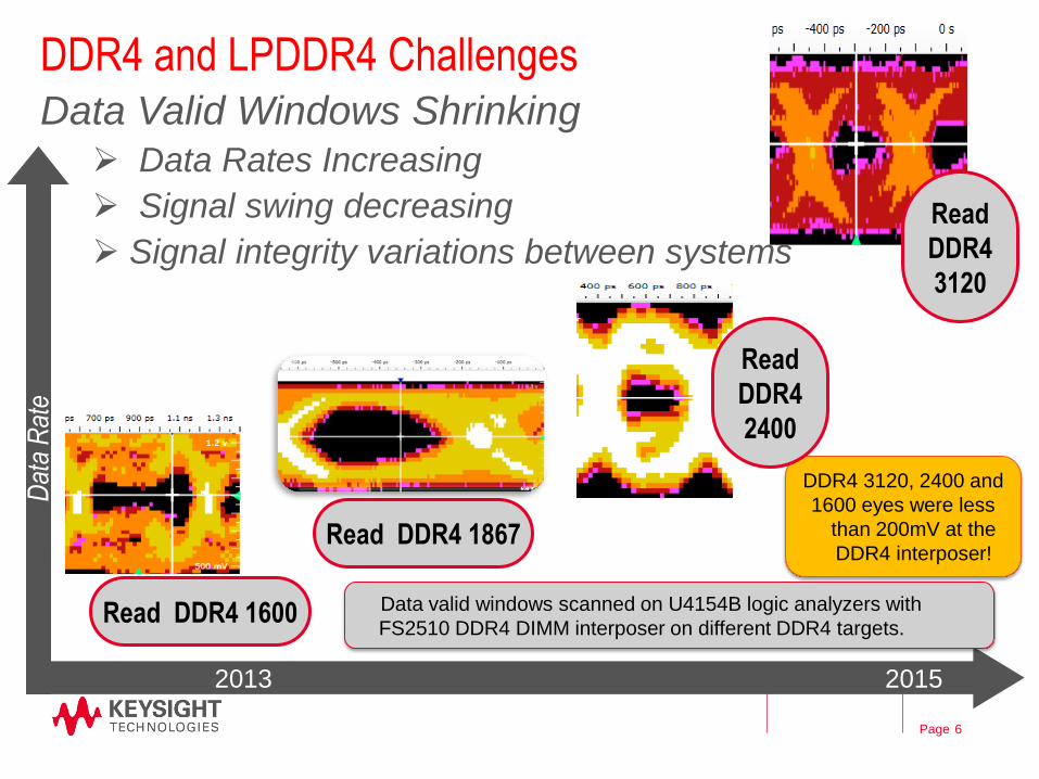
DDR4 and LPDDR4 Challenges Data Valid Windows Shrinking
Data Rates Increasing
Signal swing decreasing
Signal integrity variations between systems
Read DDR4 1600 Data valid windows scanned on U4154B logic analyzers with
FS2510 DDR4 DIMM interposer on different DDR4 targets.
Read DDR4 1867
DDR4 3120, 2400 and
1600 eyes were less
than 200mV at the
DDR4 interposer!
Read
DDR4
2400
Read
DDR4
3120
6
Page
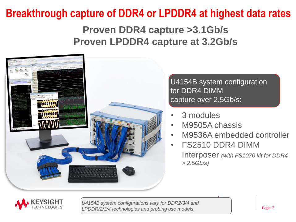
Breakthrough capture of DDR4 or LPDDR4 at highest data rates
7
• 3 modules
• M9505A chassis
• M9536A embedded controller
• FS2510 DDR4 DIMM
Interposer (with FS1070 kit for DDR4
> 2.5Gb/s)
Proven DDR4 capture >3.1Gb/s
Proven LPDDR4 capture at 3.2Gb/s
U4154B system configuration
for DDR4 DIMM
capture over 2.5Gb/s:
U4154B system configurations vary for DDR2/3/4 and
LPDDR/2/3/4 technologies and probing use models.
Page
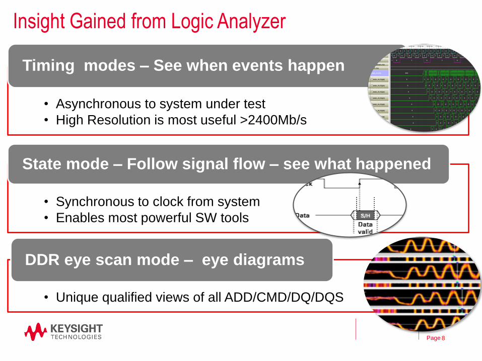
• Asynchronous to system under test
• High Resolution is most useful >2400Mb/s
Timing modes – See when events happen
• Synchronous to clock from system
• Enables most powerful SW tools
State mode – Follow signal flow – see what happened
• Unique qualified views of all ADD/CMD/DQ/DQS
DDR eye scan mode – eye diagrams
Sept 18, 2012
Insight Gained from Logic Analyzer
8
Page
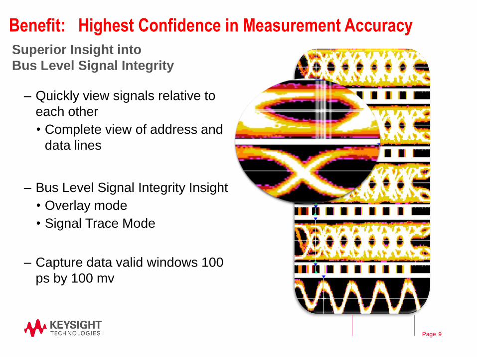
Benefit: Highest Confidence in Measurement Accuracy
Superior Insight into
Bus Level Signal Integrity
– Quickly view signals relative to
each other
• Complete view of address and
data lines
– Bus Level Signal Integrity Insight
• Overlay mode
• Signal Trace Mode
– Capture data valid windows 100
ps by 100 mv
9
Page
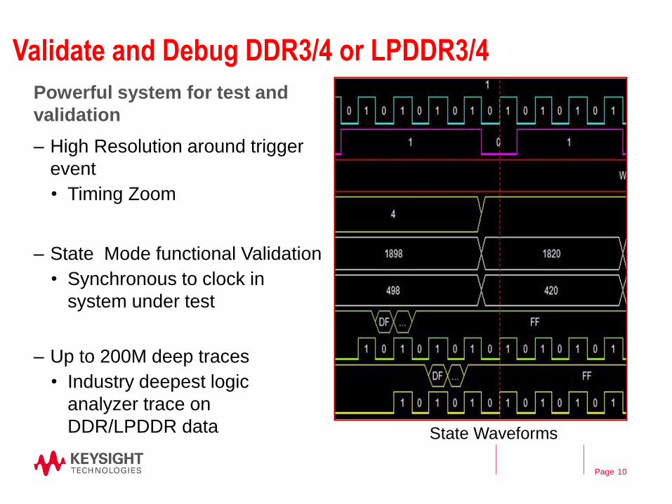
Validate and Debug DDR3/4 or LPDDR3/4
Powerful system for test and
validation
– High Resolution around trigger
event
• Timing Zoom
– State Mode functional Validation
• Synchronous to clock in
system under test
– Up to 200M deep traces
• Industry deepest logic
analyzer trace on
DDR/LPDDR data
10
State Waveforms
Page
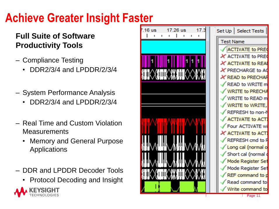
Achieve Greater Insight Faster
Full Suite of Software
Productivity Tools
– Compliance Testing
• DDR2/3/4 and LPDDR/2/3/4
– System Performance Analysis
• DDR2/3/4 and LPDDR/2/3/4
– Real Time and Custom Violation
Measurements
• Memory and General Purpose
Applications
– DDR and LPDDR Decoder Tools
• Protocol Decoding and Insight
11
State Waveforms
Page
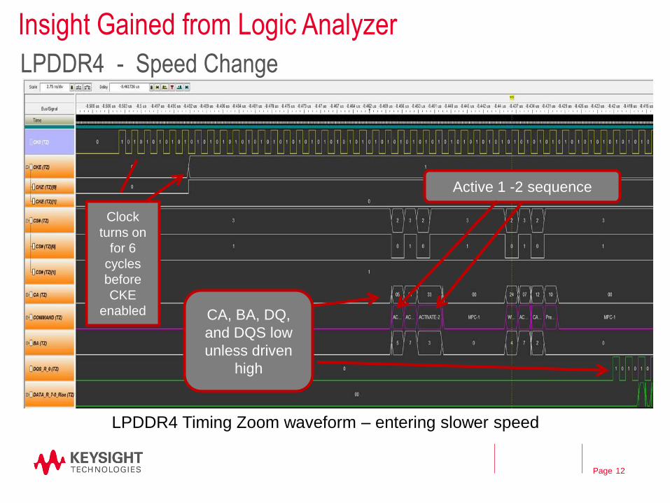
LPDDR4 - Speed Change
12
LPDDR4 Timing Zoom waveform – entering slower speed
Clock
turns on
for 6
cycles
before
CKE
enabled CA, BA, DQ,
and DQS low
unless driven
high
Active 1 -2 sequence
Insight Gained from Logic Analyzer
Page
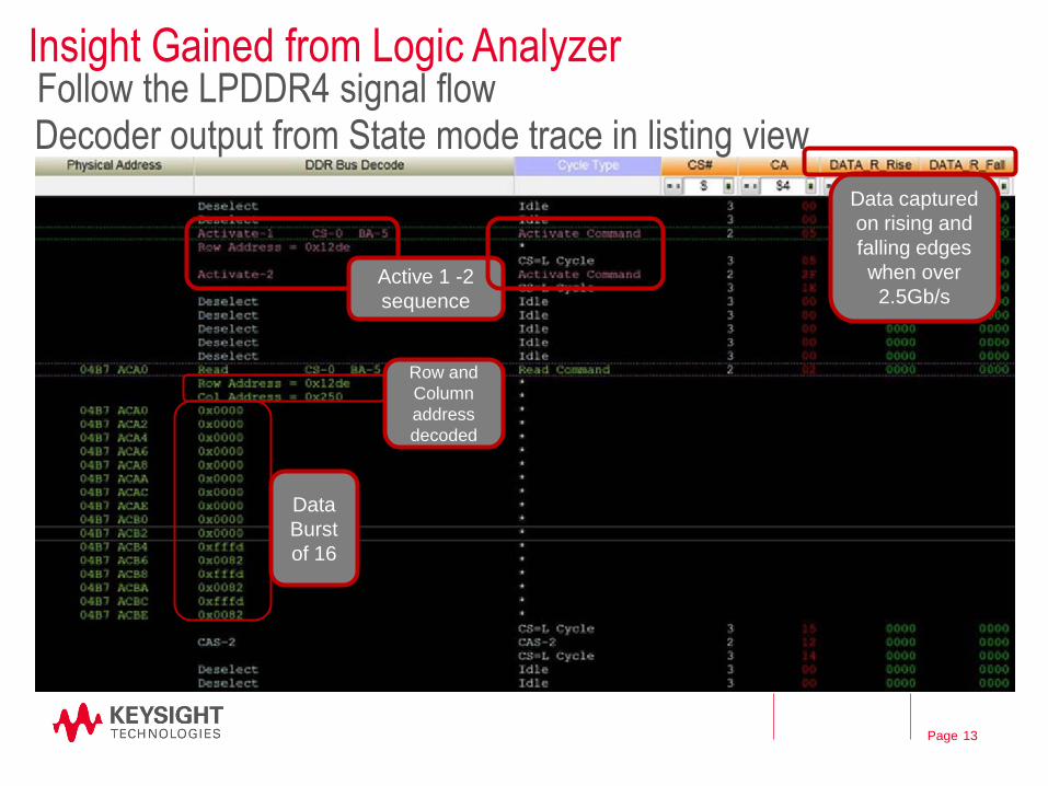
Follow the LPDDR4 signal flow
13
Decoder output from State mode trace in listing view
Data
Burst
of 16
Active 1 -2
sequence
Data captured
on rising and
falling edges
when over
2.5Gb/s
Row and
Column
address
decoded
Insight Gained from Logic Analyzer
Page 14
Agenda – Overview
• Benefits and challenges for DDR4 and LPDDR4 >2400Mb/s
• Breakthrough Insight Gained from Logic Analyzer
– Techniques to address debug and validation challenges
• DDR Eye Scan insight
• DDR4 >3.1 Gb/s DIMM system
- Tuning tool
- Waveforms and Burst Trigger
- View Initialization
- Follow the initialization signal flow
- Compliance and Performance Tools
– Successful logic analyzer probing techniques for higher data rates
– DDR Solution Overview, Recommendations, & Q&A
Page
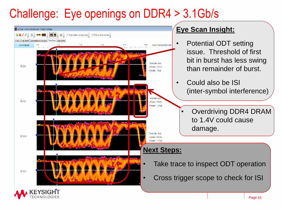
Challenge: Eye openings on DDR4 > 3.1Gb/s
Next Steps:
• Take trace to inspect ODT operation
• Cross trigger scope to check for ISI
Eye Scan Insight:
• Potential ODT setting
issue. Threshold of first
bit in burst has less swing
than remainder of burst.
• Could also be ISI
(inter-symbol interference)
• Overdriving DDR4 DRAM
to 1.4V could cause
damage.
15
Page
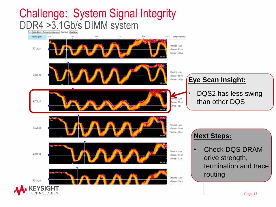
Challenge: System Signal Integrity
16
DDR4 >3.1Gb/s DIMM system
Eye Scan Insight:
• DQS2 has less swing
than other DQS
Next Steps:
• Check DQS DRAM
drive strength,
termination and trace
routing

Page
Challenge: Achieving Correct Signal Transitions
Next Steps:
• SW work around:
– Do not use BG1 = 1
– Limits address space
• Long term: HW fix required
Eye Scan Insight
DDR4 Bank group 1
Transitioning incorrectly
Symptom: Data Corruption on DDR4 system
17
Page
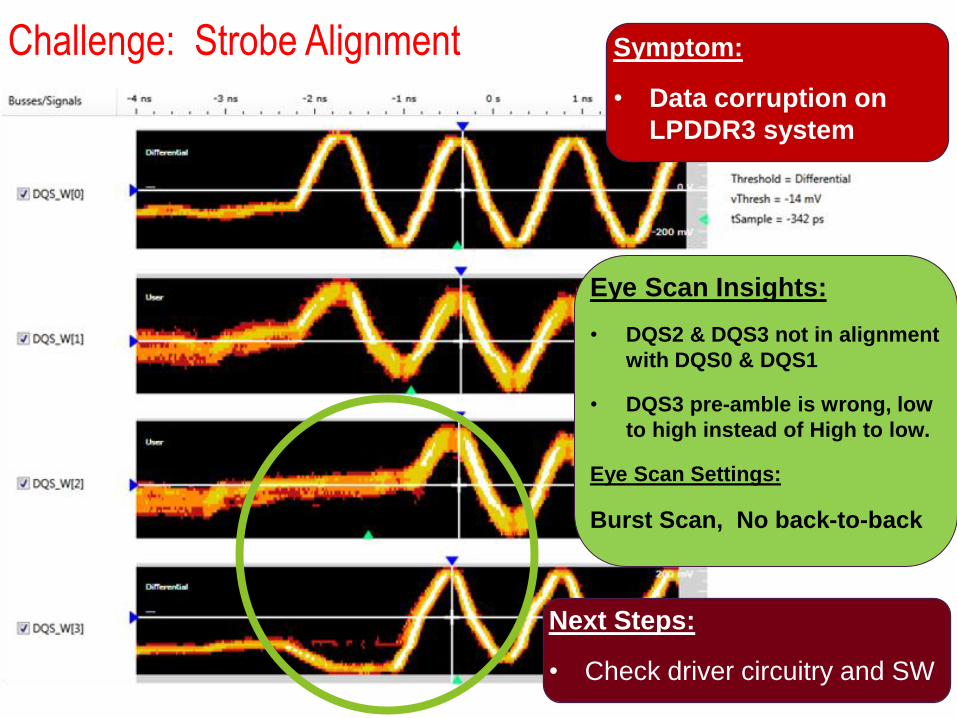
Challenge: Strobe Alignment
January 2014
Eye Scan Insights:
• DQS2 & DQS3 not in alignment
with DQS0 & DQS1
• DQS3 pre-amble is wrong, low
to high instead of High to low.
Eye Scan Settings:
Burst Scan, No back-to-back
Symptom:
• Data corruption on
LPDDR3 system
Next Steps:
• Check driver circuitry and SW
Page
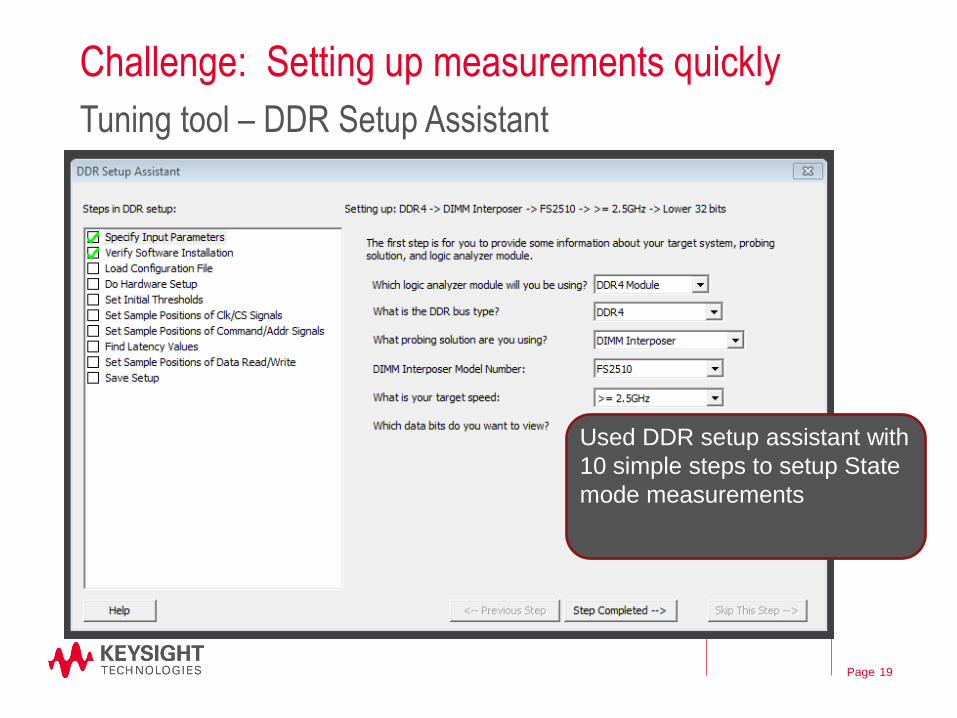
Challenge: Setting up measurements quickly
19
Tuning tool – DDR Setup Assistant
Used DDR setup assistant with
10 simple steps to setup State
mode measurements
Page
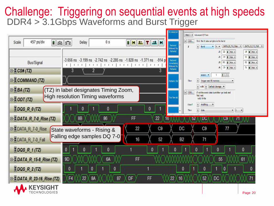
Challenge: Triggering on sequential events at high speeds
20
DDR4 > 3.1Gbps Waveforms and Burst Trigger
State waveforms - Rising &
Falling edge samples DQ 7-0
(TZ) in label designates Timing Zoom,
High resolution Timing waveforms
Page
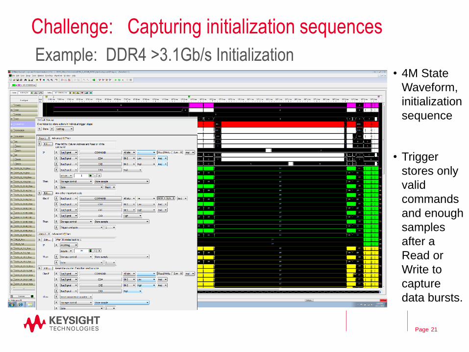
Challenge: Capturing initialization sequences
• 4M State
Waveform,
initialization
sequence
• Trigger
stores only
valid
commands
and enough
samples
after a
Read or
Write to
capture
data bursts.
21
Example: DDR4 >3.1Gb/s Initialization
Page
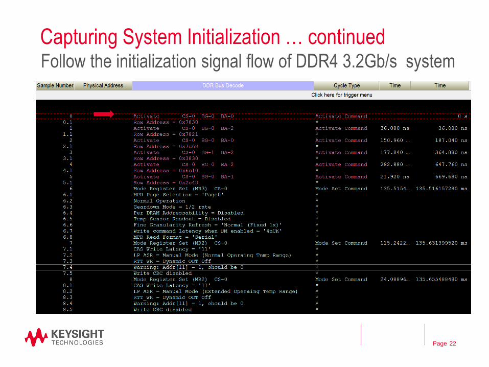
Capturing System Initialization … continued
22
Follow the initialization signal flow of DDR4 3.2Gb/s system
Page
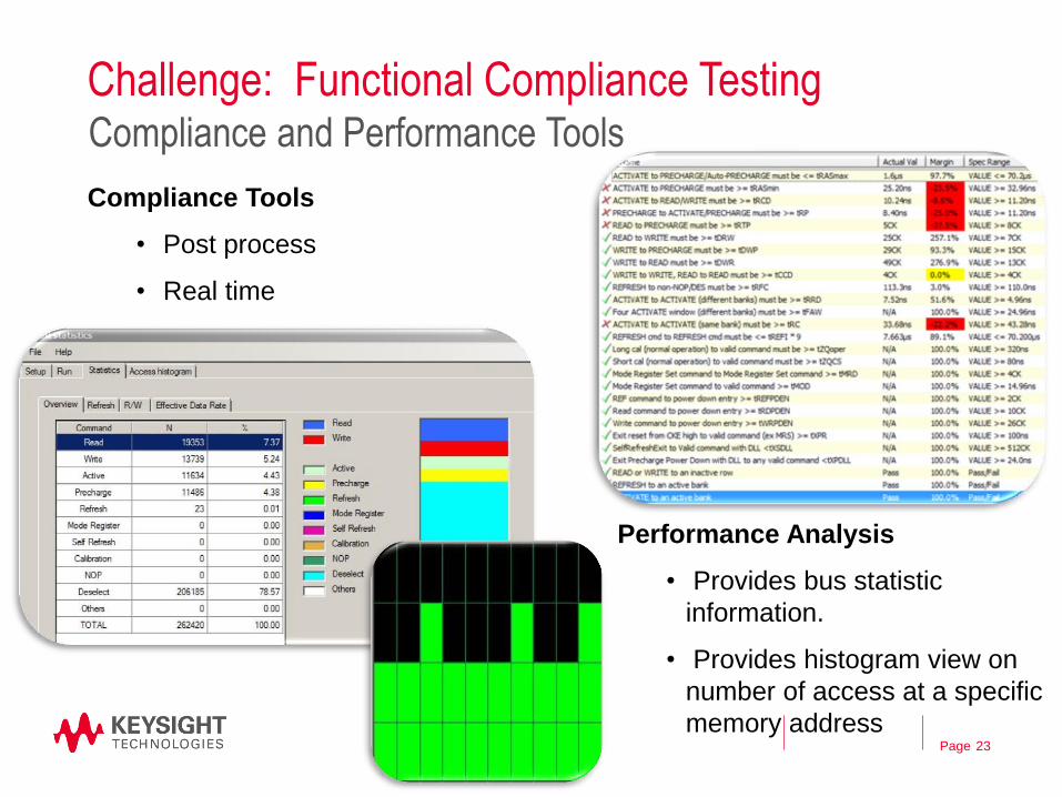
Challenge: Functional Compliance Testing
23
Compliance and Performance Tools
Compliance Tools
• Post process
• Real time
Performance Analysis
• Provides bus statistic
information.
• Provides histogram view on
number of access at a specific
memory address
Page 24
Agenda – Overview
• Benefits and challenges for DDR4 and LPDDR4 >2400Mb/s
• Breakthrough Insight Gained from Logic Analyzer
– Techniques to address debug and validation challenges
• DDR Eye Scan insight
• DDR4 >3.1 Gb/s DIMM system
- Tuning tool
- Waveforms and Burst Trigger
- View Initialization
- Follow the initialization signal flow
- Compliance and Performance Tools
– Successful logic analyzer probing techniques for higher data rates
– DDR Solution Overview, Recommendations, & Q&A
Page
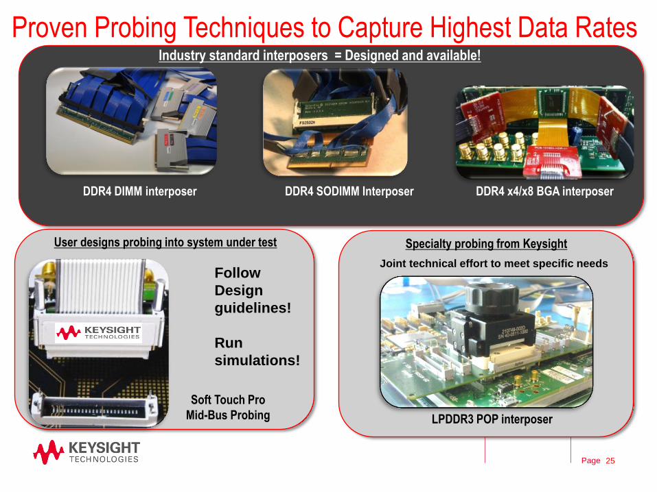
DDR4 x4/x8 BGA interposer
Soft Touch Pro
Mid-Bus Probing
DDR4 SODIMM Interposer DDR4 DIMM interposer
LPDDR3 POP interposer
Specialty probing from Keysight User designs probing into system under test
Proven Probing Techniques to Capture Highest Data Rates
Industry standard interposers = Designed and available!
Follow
Design
guidelines!
Run
simulations!
Joint technical effort to meet specific needs
Aug 6, 2013
MemCon 25
Page
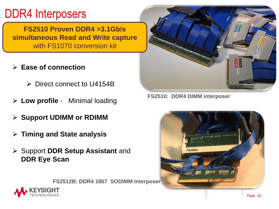
DDR4 Interposers
Ease of connection
Direct connect to U4154B
Low profile - Minimal loading
Support UDIMM or RDIMM
Timing and State analysis
Support DDR Setup Assistant and
DDR Eye Scan
FS2510: DDR4 DIMM interposer
FS2512B: DDR4 1867 SODIMM interposer
FS2510 Proven DDR4 >3.1Gb/s
simultaneous Read and Write capture
with FS1070 conversion kit
26
Page
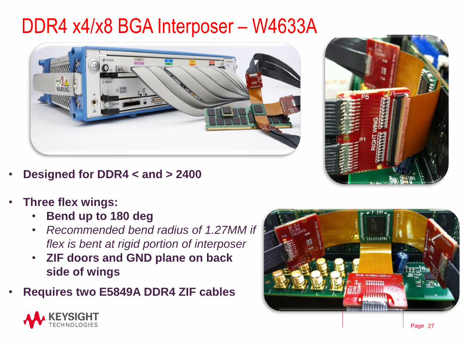
• Designed for DDR4 < and > 2400
• Three flex wings:
• Bend up to 180 deg
• Recommended bend radius of 1.27MM if
flex is bent at rigid portion of interposer
• ZIF doors and GND plane on back
side of wings
• Requires two E5849A DDR4 ZIF cables
DDR4 x4/x8 BGA Interposer – W4633A
MemCon
Aug 6, 2013
27
Page
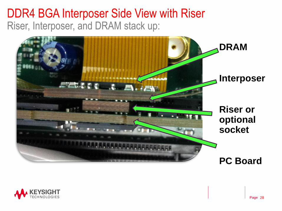
DDR4 BGA Interposer Side View with Riser Riser, Interposer, and DRAM stack up:
DRAM
Interposer
Riser or optional socket
PC Board
28
Page
• SW configurations are different for < > 2.5Gb/s
• Because trigger sequencer operates up to 2.5GHz
• Below 2.5Gb/s clock U4154B using both edges of CK0
• Above 2.5Gb/s clock U4154B using one edge of CK0
• Dual sample mode used for DQ Rising edge and falling edge
samples
• Double probing of DQ signals used for simultaneous R/W data capture with
independent thresholds
• For > 2.5Gb/s - Use Rising and Falling Read / Write Data labels in
waveform
• Decoder re-assembles Rising and Falling samples
• Above 2.5Gb/s State mode capture of CK0, CK1, and DQS don’t toggle
• They are only sampled once on each clock cycle.
• Timing Zoom and DDR eye scan used to view CK0, CK1, and DQS
Probing Techniques: U4154B State Mode > 2.5Gb/s Considerations for designing mid-bus probing
29
Page
• Run simulations on entire system with and without probing.
Ensure loading on system will be tolerated
Ensure adequate eye for logic analyzer data valid window
(minimum 100ps x 100mV for Keysight U4154B)
• Ensure signal routing meets logic analyzer requirements
Clock routed to clock input
Clock qualifier (CKE) routing into clock qualifier inputs
Route RESET to clock input on Pod 7 of clocking module as clock qualifier
Probing Techniques: U4154B State Mode > 2.5Gb/s Considerations for designing mid-bus probing continued…
30
Page
Probing Techniques: U4154B State Mode > 2.5Gb/s Considerations for designing mid-bus probing continued…
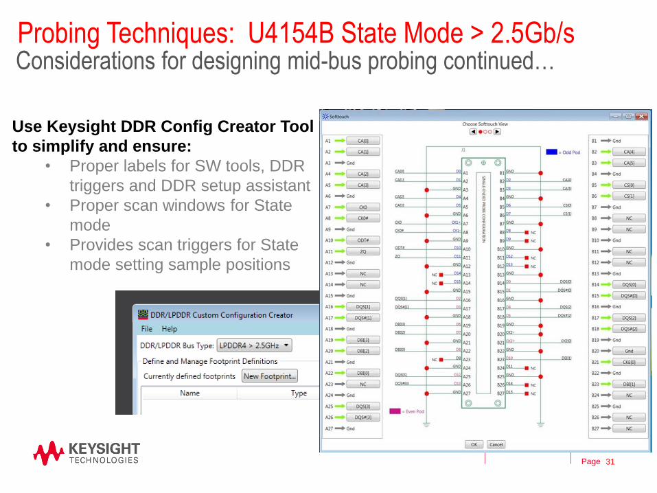
Use Keysight DDR Config Creator Tool
to simplify and ensure:
• Proper labels for SW tools, DDR
triggers and DDR setup assistant
• Proper scan windows for State
mode
• Provides scan triggers for State
mode setting sample positions
31
Page
•Placing the Soft Touch connectors close to the DRAM generally provides
better eyes than mid-bus:
•Drivers in the DRAM are typically weaker than the Memory controller drivers
•Location near the DRAM minimizes reflections
•Ideal locations would be ADD/CMD/DQ Write at DRAM and DQ Read at
memory controller
•Use flow-through routing whenever possible.
•Keep stubs from inner trace layers to pads (using vias) to a minimum in
number and length.
•Stubs increase loading and reflections resulting in degraded eyes.
•Distance between buried Tip R and mid-bus probe will act as a low pass filter
and degrade the bandwidth of signals into the logic analyzer.
Probing Techniques: U4154B State Mode > 2.5Gb/s Mid-Bus Routing Recommendations
32
Page 33
Agenda – Overview
• Benefits and challenges for DDR4 and LPDDR4 >2400Mb/s
• Breakthrough Insight Gained from Logic Analyzer
– Techniques to address debug and validation challenges
• DDR Eye Scan insight
• DDR4 >3.1 Gb/s DIMM system
- Tuning tool
- Waveforms and Burst Trigger
- View Initialization
- Follow the initialization signal flow
- Compliance and Performance Tools
– Successful logic analyzer probing techniques for higher data rates
– DDR Solution Overview, Recommendations, Q&A
Page
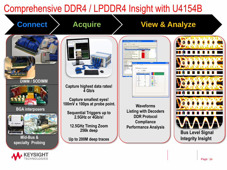
Connect Acquire View & Analyze
Comprehensive DDR4 / LPDDR4 Insight with U4154B
BGA interposers
Mid-Bus &
specialty Probing
Waveforms
Listing with Decoders
DDR Protocol
Compliance
Performance Analysis
Bus Level Signal
Integrity Insight
Capture highest data rates! 4 Gb/s
Capture smallest eyes!
100mV x 100ps at probe point.
Sequential Triggers up to 2.5GHz or 4Gb/s!
12.5GHz Timing Zoom
256k deep
Up to 200M deep traces
DIMM / SODIMM
Interposers
34
Page
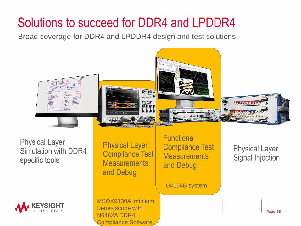
Solutions to succeed for DDR4 and LPDDR4
35
Broad coverage for DDR4 and LPDDR4 design and test solutions
Physical Layer Simulation with DDR4 specific tools
Physical Layer Compliance Test Measurements and Debug
Functional Compliance Test Measurements and Debug
Physical Layer Signal Injection
MSOX9130A Infiniium
Series scope with
N6462A DDR4
Compliance Software
U4154B system
Page
Breakthrough Digital and Analog Signal Display
36
• One instrument with time
correlated digital and
analog view.
• Best separation of
Read/Write eyes for
parametric
measurements.
• Simultaneous capture of
16 ADD/CMD and 4
DQS/DQ
MSO mixed signal oscilloscope
Page
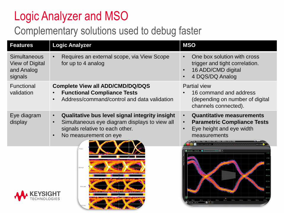
Logic Analyzer and MSO
37
Complementary solutions used to debug faster Features Logic Analyzer MSO
Simultaneous
View of Digital
and Analog
signals
• Requires an external scope, via View Scope
for up to 4 analog
• One box solution with cross
trigger and tight correlation.
• 16 ADD/CMD digital
• 4 DQS/DQ Analog
Functional
validation
Complete View all ADD/CMD/DQ/DQS
• Functional Compliance Tests
• Address/command/control and data validation
Partial view
• 16 command and address
(depending on number of digital
channels connected).
Eye diagram
display
• Qualitative bus level signal integrity insight
• Simultaneous eye diagram displays to view all
signals relative to each other.
• No measurement on eye
• Quantitative measurements
• Parametric Compliance Tests
• Eye height and eye width
measurements

Page
Recommendations:
• Join JEDEC and download DDR4 and/or LPDDR4
Specifications for your design http://www.jedec.org/
• Follow design guidelines from chip vendors
• Simulate your system with and without probing
• Perform physical layer compliance tests with scope
• Perform functional layer compliance tests with logic
analyzer
• Use both scope and logic analyzer for debug and test
Aug 6, 2013
MemCon
38
Page
Contact Keysight
Aug 6, 2013
Product Selection and Configuration Assistance,
Education and Training
US phone: 1 800 829-4444 Press # then 2
Hours: 8:00am – 8:00pm ET, Mon - Fri
For more information on Keysight Technologies’ products, applications or
services, please contact your local Keysight office. The complete list is
available at:
www.Keysight.com/find/contactus
39
Page
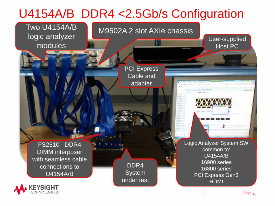
U4154A/B DDR4 <2.5Gb/s Configuration
User-supplied
Host PC
Two U4154A/B
logic analyzer
modules
FS2510 DDR4
DIMM interposer
with seamless cable
connections to
U4154A/B
M9502A 2 slot AXIe chassis
DDR4
System
under test
PCI Express
Cable and
adapter
Logic Analyzer System SW
common to:
U4154A/B
16900 series
16800 series
PCI Express Gen3
HDMI
40