Embed Size (px)
Citation preview
BRISC-V: An Open-Source Architecture Design SpaceExploration Toolbox
Sahan Bandara, Alan Ehret, Donato Kava and Michel A. KinsyAdaptive and Secure Computing Systems (ASCS) Laboratory
Department of Electrical and Computer Engineering, Boston UniversityBoston, Massachusetts, 02134, USA
{sahanb, ehretaj, dkava, mkinsy}@bu.edu
ABSTRACTIn this work, we introduce a platform for register-transfer level(RTL) architecture design space exploration. The platform is anopen-source, parameterized, synthesizable set of RTL modules fordesigning RISC-V based single and multi-core architecture systems.The platform is designed with a high degree of modularity. It pro-vides highly-parameterized, composable RTL modules for fast andaccurate exploration of different RISC-V based core complexities,multi-level caching and memory organizations, system topologies,router architectures, and routing schemes. The platform can beused for both RTL simulation and FPGA based emulation. Thehardware modules are implemented in synthesizable Verilog usingno vendor-specific blocks. The platform includes a RISC-V com-piler toolchain to assist in developing software for the cores, aweb-based system configuration graphical user interface (GUI) anda web-based RISC-V assembly simulator. The platform supportsa myriad of RISC-V architectures, ranging from a simple singlecycle processor to a multi-core SoC with a complex memory hierar-chy and a network-on-chip. The modules are designed to supportincremental additions and modifications. The interfaces betweencomponents are particularly designed to allow parts of the pro-cessor such as whole cache modules, cores or individual pipelinestages, to be modified or replaced without impacting the rest ofthe system. The platform allows researchers to quickly instantiatecomplete working RISC-V multi-core systems with synthesizableRTL and make targeted modifications to fit their needs. The com-plete platform (including Verilog source code) can be downloadedat https://ascslab.org/research/briscv/explorer/explorer.html.
KEYWORDSComputer architecture design exploration, RISC-V, FPGA, Synthe-sizable, Open Source, Verilog.
1 INTRODUCTIONDesigning, building, and testing multi-core, many-core and evensingle-core processor systems is a difficult and time consuming task.Designers are faced with numerous design decisions that, whentaken as a whole, impact performance in subtle ways. With theever increasing size and complexity of multi-core and many-coresystems, the time and effort needed for development is quickly rais-ing the barrier to entry for design space exploration and research.This growing obstacle to multi-core system design creates a needfor a flexible micro-architecture design space exploration platform.However, there are many challenges involved with creating sucha platform. Salient research questions related to creating such a
platform include: (1) What aspects of a multi-core system are rele-vant to micro-architecture design space exploration? (2) How cana design space exploration platform provide ease of use and rapidexploration while maintaining the speed and accuracy of FPGA-based emulation? (3) How can the size of the design space coveredby a platform be maximized to provide support for a wide range ofsystems and research?
To address these questions and challenges, we present an open-source platform for RISC-V multi-core system micro-architecturedesign space exploration. The key components of this platform are:
• A modular, parameterized, synthesizable multi-core RISC-Vhardware system written in Verilog.
• A RISC-V toolchain to compile a user’s code for bare-metalexecution on the hardware system.
• A RISC-V assembly simulator to test a user’s software inde-pendently of the hardware system.
• A hardware system configuration graphical user interfaceto visualize and generate multi-core hardware systems.
The name of the platform is withheld to maintain anonymity.Current research that would benefit from fast micro-architecture
design space exploration ranges from the development of efficientnetwork on-chip (NoC) [12] to cache timing side channel elimina-tion [5] to heterogeneous [8] or adaptive architecture design [4].Indeed, there is still active research related to every subsystem ina multi-core design. As such, our platform supports design spaceexploration for: (1) RISC-V cores, with various pipeline depths andconfigurations; (2) the cache subsystem with user selectable sizesand associativities; (3) a main memory subsystem with support foron-chip block RAM (BRAM) or off-chip memory; and (4) a parame-terized on-chip network supporting a variety of router designs androuting algorithms.
The hardware system is written in synthesizable Verilog withno vendor specific IP blocks. This implementation enables RTLsimulation, in addition to the fast FPGA-based emulation necessaryfor large, yet accurate, design space exploration. Parameterizationand modularity allow for rapid changes to the design of the system.Individual modules (e.g. core pipeline stages or cache replacementpolicies) as well as whole subsystems (e.g. core, cache or NoC de-signs) can be customized or replaced independently of each other.This allows users to make changes to their relevant systems withoutthe need to modify or understand implementation details of otheraspects of the system. The platform provides multiple implemen-tations of core, cache, memory and NoC subsystems for users tochoose from. Parameterized modules allow users to quickly changesettings of the system, such as cache size, cache associativity, or
arX
iv:1
908.
0999
2v1
[cs
.AR
] 2
7 A
ug 2
019
number of cores. Such parameters enable the fine tuning of a micro-architecture after the appropriate hardware modules have beenselected.
The software tools included in the platform facilitate rapid de-sign space exploration by streamlining the platform work flow.Including the necessary toolchain allows users to develop softwarefor their design space exploration quickly and run it on a variety ofsystem configurations. The platform’s RISC-V assembly simulatorcan be used to create a golden model of program execution andfine tune software before testing it on the hardware system. Thesegolden models can accelerate debugging efforts by providing anexpected execution flow. The hardware system configuration GUIallows users to select core types and features, cache sizes, and as-sociativities, bus-based or NoC- based interconnects, among manyother parameters. Visualizations of the configuration promptly giveusers an understanding of their system. Users can use the GUI togenerate an RTL implementation of the system, allowing them toeasily make and visualize changes, before producing a new design.The modularity that comes with support for interchangeable core,cache, memory, and NoC subsystems (and their internal modules)enables a wide breadth of design space for exploration, without anyRTL modifications to the base platform. In order to maximize theexplorable design space, every aspect of the platform is open-source.Users looking to expand the number of supported subsystems oradd experimental features can do so by modifying or extending theVerilog RTL of the base system.
The use of RISC-V, an open ISA that is freely available, adds ad-ditional possibilities for design space exploration with its modularnature and numerous extension specifications [14] [13]. Users canadd custom instruction set extensions to support experimental ar-chitecture features or custom hardware accelerators. The opennessand the option for custom extensions makes RISC-V an excellentISA for design space exploration. This platform uses version 2.2 ofthe RISC-V User-Level ISA [14]
The complete platform (including Verilog source code) can bedownloaded at https://ascslab.org/research/briscv/explorer/explorer.html.
2 RELATEDWORKOther work has developed configurable processors and tools tofacilitate varying degrees of design space exploration. One such tool,Heracles [7] [6], is based on the MIPS ISA and runs on theWindowsoperating system. Everything needed to create a synthesizablesystem is included with Heracles. A GUI enables users to specifytheir system and generate Verilog code for it. Two core types, eachwith one or two hardware threads, can be selected for use in multi-core systems. A dummy core is included to test different on-chipnetwork designs. Cache hierarchies can involve one or two levelsof direct mapped caches. A cross compiler allows programmersto write parallel code for a multi-core MIPS architecture. A widevariety of NoC routing configuration options are available in theNoC configuration of Heracles.
Heracles and our platform share similar goals, however, Heraclesis more limited in the number of core and cache configurationsavailable. Additionally, the use of RISC-V in our platform makesextending the ISA easier, given RISC-V’s opcodes dedicated to user
defined instructions [14]. These improvements in our platformcreate a richer and larger explorable design space.
The Soft Processor Rapid Exploration Environment (SPREE) toolprovides another MIPS-based design space exploration tool [9] [16].SPREE explores such trade-offs in micro-architectural details aspipeline depth, hazard detection implementation, as well as ISAfeatures like branch delay slots and application-specific registermanagement. However, the design space covered by SPREE is lim-ited to the cores in a processing system. Additionally, only singlecore designs are supported by SPREE. Our platform offers a morecomplete design space exploration, with support for multi-coresystems with core, cache, memory and NoC configuration options.
The free and open nature of RISC-V means that numerous open-source implementations are available. A few of these, for example, asize optimized core named PicoRV32 [15] and a Linux capable corenamed RV12 from RoaLogic [11], include SoCs generated with theRocket Chip Generator [3]. Many more implementations exist, butfor brevity they are omitted. While the RISC-V implementationsmentioned offer some level of configuration, none of them supportmulti-core, cache, or NoC design space exploration in the wayour platform does. Table 1 compares the configuration optionsand features available for design space exploration in each of thereferenced works.
PicoRV32
RV12
RocketChip
SPREEHeracles
Our Platform
Core ✓ ✓ ✓ ✓ ✓ ✓Cache ✓ ✓ ✓ ✓
Memory ✓ ✓Interconnect ✓ ✓Multi-Core ✓ ✓ ✓
Extensible ISA ✓ ✓ ✓ ✓GUI ✓ ✓
Table 1: A comparison of configurable subsystems and fea-tures available in popular configurable processors.
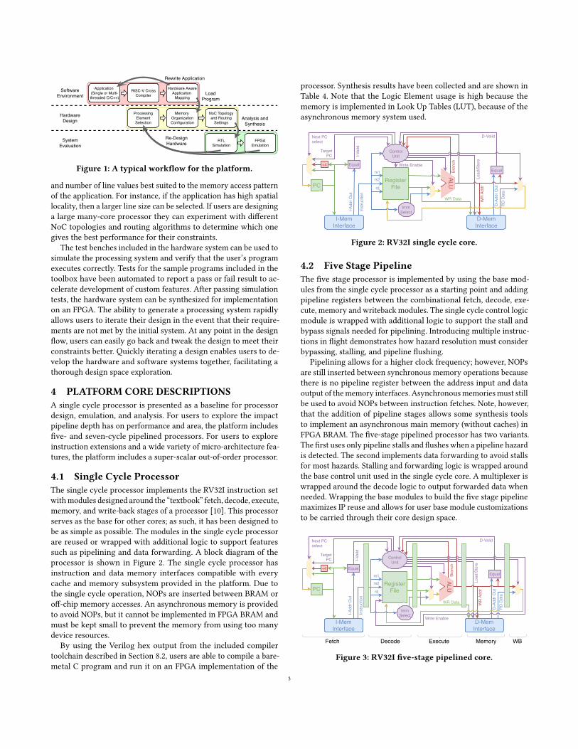
3 PLATFORM OVERVIEWA typical workflow in the platform (shown in Figure 1) starts withdeveloping the software application to be run on the hardware sys-tem. Software is compiled with either the GNU or LLVM compilertoolchain for RISC-V. The included compiler scripts support simplemulti-processing and multi-threading environments.
After developing the application, users can determine perfor-mance requirements as well as power and area constraints. Giventhe system requirements, a user can begin setting parameters forthe core, cache, memory and NoC subsystems. Users can set theseparameters with the hardware configuration GUI discussed in Sec-tion 8.1. Users requiring a small processor to handle embeddedapplications might select a small single cycle core with a simpleBRAM memory, while a user developing a large distributed multi-core system could opt for the more complex pipelined or out-of-order cores, with large caches and a memory controller for off-chipmemory. Users developing a system for a single application canoptimize the cache subsystem by selecting line size, associativity,
2
Application (Single or Multi- threaded C/C++)
RISC-V Cross Compiler
Hardware AwareApplication
Mapping
Processing Element Selection
Memory Organization Configuration
NoC Topology and Routing
Settings
RTL Simulation
FPGA Emulation
SoftwareEnvironment
Hardware Design
System Evaluation
LoadProgram
Analysis andSynthesis
Rewrite Application
Re-Design Hardware
Figure 1: A typical workflow for the platform.
and number of line values best suited to the memory access patternof the application. For instance, if the application has high spatiallocality, then a larger line size can be selected. If users are designinga large many-core processor they can experiment with differentNoC topologies and routing algorithms to determine which onegives the best performance for their constraints.
The test benches included in the hardware system can be used tosimulate the processing system and verify that the user’s programexecutes correctly. Tests for the sample programs included in thetoolbox have been automated to report a pass or fail result to ac-celerate development of custom features. After passing simulationtests, the hardware system can be synthesized for implementationon an FPGA. The ability to generate a processing system rapidlyallows users to iterate their design in the event that their require-ments are not met by the initial system. At any point in the designflow, users can easily go back and tweak the design to meet theirconstraints better. Quickly iterating a design enables users to de-velop the hardware and software systems together, facilitating athorough design space exploration.
4 PLATFORM CORE DESCRIPTIONSA single cycle processor is presented as a baseline for processordesign, emulation, and analysis. For users to explore the impactpipeline depth has on performance and area, the platform includesfive- and seven-cycle pipelined processors. For users to exploreinstruction extensions and a wide variety of micro-architecture fea-tures, the platform includes a super-scalar out-of-order processor.
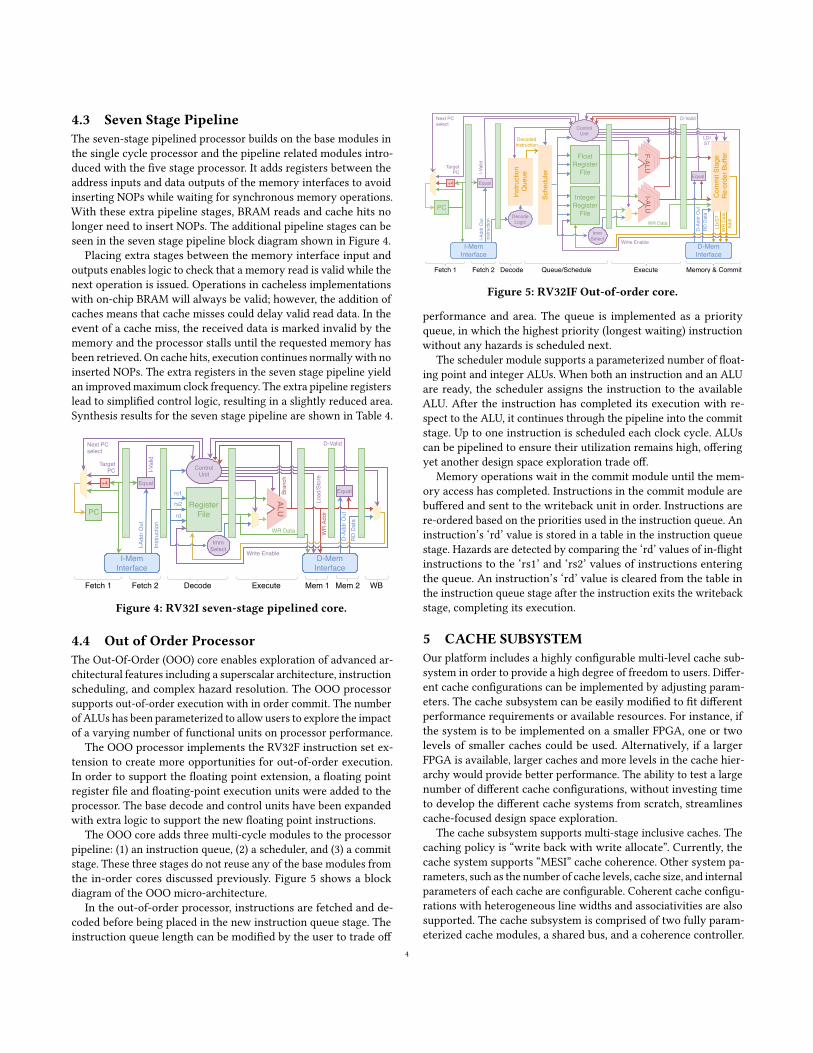
4.1 Single Cycle ProcessorThe single cycle processor implements the RV32I instruction setwithmodules designed around the “textbook” fetch, decode, execute,memory, and write-back stages of a processor [10]. This processorserves as the base for other cores; as such, it has been designed tobe as simple as possible. The modules in the single cycle processorare reused or wrapped with additional logic to support featuressuch as pipelining and data forwarding. A block diagram of theprocessor is shown in Figure 2. The single cycle processor hasinstruction and data memory interfaces compatible with everycache and memory subsystem provided in the platform. Due tothe single cycle operation, NOPs are inserted between BRAM oroff-chip memory accesses. An asynchronous memory is providedto avoid NOPs, but it cannot be implemented in FPGA BRAM andmust be kept small to prevent the memory from using too manydevice resources.
By using the Verilog hex output from the included compilertoolchain described in Section 8.2, users are able to compile a bare-metal C program and run it on an FPGA implementation of the
processor. Synthesis results have been collected and are shown inTable 4. Note that the Logic Element usage is high because thememory is implemented in Look Up Tables (LUT), because of theasynchronous memory system used.
Register File
I-Mem Interface
D-Mem Interface
rs1 Bran
ch
Write Enable
I-Val
id
Inst
ruct
ion
I-Add
r Out
Next PC select
rs2
rd
Load
/Sto
re
WR
Add
r
Control Unit
D-Valid
WR Data
RD
Dat
a D
-Add
r Out
TargetPC
Equal+4
PC
Equal
Imm Select
ALU
Figure 2: RV32I single cycle core.
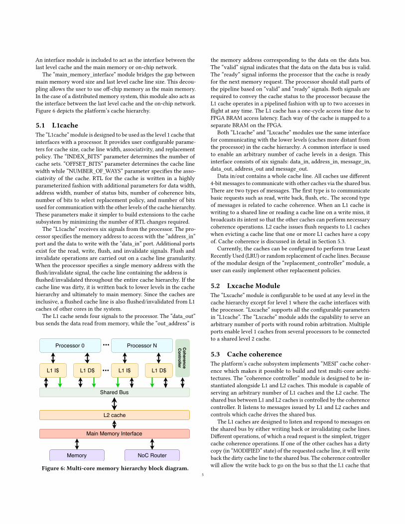
4.2 Five Stage PipelineThe five stage processor is implemented by using the base mod-ules from the single cycle processor as a starting point and addingpipeline registers between the combinational fetch, decode, exe-cute, memory and writeback modules. The single cycle control logicmodule is wrapped with additional logic to support the stall andbypass signals needed for pipelining. Introducing multiple instruc-tions in flight demonstrates how hazard resolution must considerbypassing, stalling, and pipeline flushing.
Pipelining allows for a higher clock frequency; however, NOPsare still inserted between synchronous memory operations becausethere is no pipeline register between the address input and dataoutput of thememory interfaces. Asynchronousmemoriesmust stillbe used to avoid NOPs between instruction fetches. Note, however,that the addition of pipeline stages allows some synthesis toolsto implement an asynchronous main memory (without caches) inFPGA BRAM. The five-stage pipelined processor has two variants.The first uses only pipeline stalls and flushes when a pipeline hazardis detected. The second implements data forwarding to avoid stallsfor most hazards. Stalling and forwarding logic is wrapped aroundthe base control unit used in the single cycle core. A multiplexer iswrapped around the decode logic to output forwarded data whenneeded. Wrapping the base modules to build the five stage pipelinemaximizes IP reuse and allows for user base module customizationsto be carried through their core design space.
Register File
I-Mem Interface
Fetch Decode Execute Memory WB
D-Mem Interface
rs1 Bran
ch
Write Enable
I-Val
id
Inst
ruct
ion
I-Add
r Out
Next PC select
rs2
rd
Load
/Sto
re
WR
Add
r
Control Unit
D-Valid
WR Data
RD
Dat
a D
-Add
r Out
TargetPC
Equal+4
PC
Equal
Imm Select
ALU
Figure 3: RV32I five-stage pipelined core.
3
4.3 Seven Stage PipelineThe seven-stage pipelined processor builds on the base modules inthe single cycle processor and the pipeline related modules intro-duced with the five stage processor. It adds registers between theaddress inputs and data outputs of the memory interfaces to avoidinserting NOPs while waiting for synchronous memory operations.With these extra pipeline stages, BRAM reads and cache hits nolonger need to insert NOPs. The additional pipeline stages can beseen in the seven stage pipeline block diagram shown in Figure 4.
Placing extra stages between the memory interface input andoutputs enables logic to check that a memory read is valid while thenext operation is issued. Operations in cacheless implementationswith on-chip BRAM will always be valid; however, the addition ofcaches means that cache misses could delay valid read data. In theevent of a cache miss, the received data is marked invalid by thememory and the processor stalls until the requested memory hasbeen retrieved. On cache hits, execution continues normally with noinserted NOPs. The extra registers in the seven stage pipeline yieldan improvedmaximum clock frequency. The extra pipeline registerslead to simplified control logic, resulting in a slightly reduced area.Synthesis results for the seven stage pipeline are shown in Table 4.
Register File
I-Mem Interface
Fetch 1 Fetch 2 Decode Execute Mem 1 Mem 2 WB
D-Mem Interface
rs1 Bran
ch
Write Enable
I-Val
id
Inst
ruct
ion
I-Add
r Out
Next PC select
rs2
rd
Load
/Sto
re
WR
Add
r
Control Unit
D-Valid
WR Data
RD
Dat
a D
-Add
r Out
TargetPC
Equal+4
PC
Equal
Imm Select
ALU
Figure 4: RV32I seven-stage pipelined core.
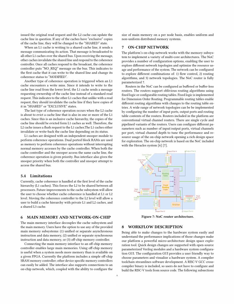
4.4 Out of Order ProcessorThe Out-Of-Order (OOO) core enables exploration of advanced ar-chitectural features including a superscalar architecture, instructionscheduling, and complex hazard resolution. The OOO processorsupports out-of-order execution with in order commit. The numberof ALUs has been parameterized to allow users to explore the impactof a varying number of functional units on processor performance.
The OOO processor implements the RV32F instruction set ex-tension to create more opportunities for out-of-order execution.In order to support the floating point extension, a floating pointregister file and floating-point execution units were added to theprocessor. The base decode and control units have been expandedwith extra logic to support the new floating point instructions.
The OOO core adds three multi-cycle modules to the processorpipeline: (1) an instruction queue, (2) a scheduler, and (3) a commitstage. These three stages do not reuse any of the base modules fromthe in-order cores discussed previously. Figure 5 shows a blockdiagram of the OOO micro-architecture.
In the out-of-order processor, instructions are fetched and de-coded before being placed in the new instruction queue stage. Theinstruction queue length can be modified by the user to trade off
Integer
Register File
I-Mem Interface
Fetch 1 Fetch 2 Decode Execute Memory & Commit
D-Mem Interface
Write Enable
I-Val
id
Inst
ruct
ion
I-Add
r Out
Next PC select
LD/ ST
Addr
Control Unit
D-Valid
WR Data
RD
Dat
a D
-Add
r Out
TargetPC
Equal+4
PC
Equal
Imm Select
Inst
ruct
ion
Q
ueue
Sche
dule
r
Float Register
File
I-ALU
F-ALU
Decoded Instruction
Decode Logic
Com
mit
Stag
e
Re-
orde
r Buf
fer
Queue/Schedule
WR
Dat
a LD
/ST
Figure 5: RV32IF Out-of-order core.
performance and area. The queue is implemented as a priorityqueue, in which the highest priority (longest waiting) instructionwithout any hazards is scheduled next.
The scheduler module supports a parameterized number of float-ing point and integer ALUs. When both an instruction and an ALUare ready, the scheduler assigns the instruction to the availableALU. After the instruction has completed its execution with re-spect to the ALU, it continues through the pipeline into the commitstage. Up to one instruction is scheduled each clock cycle. ALUscan be pipelined to ensure their utilization remains high, offeringyet another design space exploration trade off.
Memory operations wait in the commit module until the mem-ory access has completed. Instructions in the commit module arebuffered and sent to the writeback unit in order. Instructions arere-ordered based on the priorities used in the instruction queue. Aninstruction’s ‘rd’ value is stored in a table in the instruction queuestage. Hazards are detected by comparing the ‘rd’ values of in-flightinstructions to the ‘rs1’ and ‘rs2’ values of instructions enteringthe queue. An instruction’s ‘rd’ value is cleared from the table inthe instruction queue stage after the instruction exits the writebackstage, completing its execution.
5 CACHE SUBSYSTEMOur platform includes a highly configurable multi-level cache sub-system in order to provide a high degree of freedom to users. Differ-ent cache configurations can be implemented by adjusting param-eters. The cache subsystem can be easily modified to fit differentperformance requirements or available resources. For instance, ifthe system is to be implemented on a smaller FPGA, one or twolevels of smaller caches could be used. Alternatively, if a largerFPGA is available, larger caches and more levels in the cache hier-archy would provide better performance. The ability to test a largenumber of different cache configurations, without investing timeto develop the different cache systems from scratch, streamlinescache-focused design space exploration.
The cache subsystem supports multi-stage inclusive caches. Thecaching policy is “write back with write allocate”. Currently, thecache system supports “MESI” cache coherence. Other system pa-rameters, such as the number of cache levels, cache size, and internalparameters of each cache are configurable. Coherent cache configu-rations with heterogeneous line widths and associativities are alsosupported. The cache subsystem is comprised of two fully param-eterized cache modules, a shared bus, and a coherence controller.
4
An interface module is included to act as the interface between thelast level cache and the main memory or on-chip network.
The “main_memory_interface” module bridges the gap betweenmain memory word size and last level cache line size. This decou-pling allows the user to use off-chip memory as the main memory.In the case of a distributed memory system, this module also acts asthe interface between the last level cache and the on-chip network.Figure 6 depicts the platform’s cache hierarchy.
5.1 L1cacheThe “L1cache”module is designed to be used as the level 1 cache thatinterfaces with a processor. It provides user configurable parame-ters for cache size, cache line width, associativity, and replacementpolicy. The “INDEX_BITS” parameter determines the number ofcache sets. “OFFSET_BITS” parameter determines the cache linewidth while “NUMBER_OF_WAYS” parameter specifies the asso-ciativity of the cache. RTL for the cache is written in a highlyparameterized fashion with additional parameters for data width,address width, number of status bits, number of coherence bits,number of bits to select replacement policy, and number of bitsused for communication with the other levels of the cache hierarchy.These parameters make it simpler to build extensions to the cachesubsystem by minimizing the number of RTL changes required.
The “L1cache” receives six signals from the processor. The pro-cessor specifies the memory address to access with the “address_in”port and the data to write with the “data_in” port. Additional portsexist for the read, write, flush, and invalidate signals. Flush andinvalidate operations are carried out on a cache line granularity.When the processor specifies a single memory address with theflush/invalidate signal, the cache line containing the address isflushed/invalidated throughout the entire cache hierarchy. If thecache line was dirty, it is written back to lower levels in the cachehierarchy and ultimately to main memory. Since the caches areinclusive, a flushed cache line is also flushed/invalidated from L1caches of other cores in the system.
The L1 cache sends four signals to the processor. The “data_out”bus sends the data read from memory, while the “out_address” is
L1 I$ L1 D$
L2 cache
Memory
Processor 0
L1 I$ L1 D$
Processor N
NoC Router
Shared Bus
Main Memory Interface
Coherence
Controller ...
...
Figure 6: Multi-core memory hierarchy block diagram.
the memory address corresponding to the data on the data bus.The “valid” signal indicates that the data on the data bus is valid.The “ready” signal informs the processor that the cache is readyfor the next memory request. The processor should stall parts ofthe pipeline based on “valid” and “ready” signals. Both signals arerequired to convey the cache status to the processor because theL1 cache operates in a pipelined fashion with up to two accesses inflight at any time. The L1 cache has a one-cycle access time due toFPGA BRAM access latency. Each way of the cache is mapped to aseparate BRAM on the FPGA.
Both “L1cache” and “Lxcache” modules use the same interfacefor communicating with the lower levels (caches more distant fromthe processor) in the cache hierarchy. A common interface is usedto enable an arbitrary number of cache levels in a design. Thisinterface consists of six signals: data_in, address_in, message_in,data_out, address_out and message_out.
Data in/out contains a whole cache line. All caches use different4-bit messages to communicate with other caches via the shared bus.There are two types of messages. The first type is to communicatebasic requests such as read, write back, flush, etc.. The second typeof messages is related to cache coherence. When an L1 cache iswriting to a shared line or reading a cache line on a write miss, itbroadcasts its intent so that the other caches can perform necessarycoherence operations. L2 cache issues flush requests to L1 cacheswhen evicting a cache line that one or more L1 caches have a copyof. Cache coherence is discussed in detail in Section 5.3.
Currently, the caches can be configured to perform true LeastRecently Used (LRU) or random replacement of cache lines. Becauseof the modular design of the “replacement_controller” module, auser can easily implement other replacement policies.
5.2 Lxcache ModuleThe “Lxcache” module is configurable to be used at any level in thecache hierarchy except for level 1 where the cache interfaces withthe processor. “Lxcache” supports all the configurable parametersin “L1cache”. The “Lxcache” module adds the capability to serve anarbitrary number of ports with round robin arbitration. Multipleports enable level 1 caches from several processors to be connectedto a shared level 2 cache.
5.3 Cache coherenceThe platform’s cache subsystem implements “MESI” cache coher-ence which makes it possible to build and test multi-core archi-tectures. The “coherence controller” module is designed to be in-stantiated alongside L1 and L2 caches. This module is capable ofserving an arbitrary number of L1 caches and the L2 cache. Theshared bus between L1 and L2 caches is controlled by the coherencecontroller. It listens to messages issued by L1 and L2 caches andcontrols which cache drives the shared bus.
The L1 caches are designed to listen and respond to messages onthe shared bus by either writing back or invalidating cache lines.Different operations, of which a read request is the simplest, triggercache coherence operations. If one of the other caches has a dirtycopy (in “MODIFIED” state) of the requested cache line, it will writeback the dirty cache line to the shared bus. The coherence controllerwill allow the write back to go on the bus so that the L1 cache that
5
issued the original read request and the L2 cache can update thecache line in question. If any of the caches have “exclusive” copiesof the cache line, they will be changed to the “SHARED” state.
When an L1 cache is writing to a shared cache line, it sends amessage communicating its action. That message is broadcasted toall other L1 caches over the shared bus. Upon receiving the message,other caches invalidate the shared line and respond to the coherencecontroller. Once all caches respond to the broadcast, the coherencecontroller puts “NO_REQ” message on the bus. This indicates tothe first cache that it can write to the shared line and change itscoherence status to “MODIFIED”.
Another type of coherence operation is triggered when an L1cache encounters a write miss. Since it intends to write to thecache line read from the lower level, the L1 cache sends a messagerequesting ownership of the cache line instead of a standard readrequest. This indicates to the other L1 caches that unlike with a readrequest, they should invalidate the cache line if they have copies ofit in “SHARED” or “EXCLUSIVE” states.
The last type of coherence operation occurs when the L2 cacheis about to evict a cache line that is also in one or more of the L1caches. Since this is an inclusive cache hierarchy, the copies of thecache line should be evicted form L1 caches as well. Therefore, theL2 cache issues a flush request to the L1 caches.The L1 caches eitherinvalidate or write-back the cache line depending on its status.
L1 caches are designed with an independent snooper module toperform coherence operations. Dual ported block RAMs are usedas memory to perform coherence operations without interruptingnormal memory accesses by the cache controller. When both thecache controller and the snooper access the same cache line, thecoherence operation is given priority. Bus interface also gives thesnooper priority when both the controller and snooper attempt toaccess the shared bus.
5.4 LimitationsCurrently, cache coherence is handled at the first level of the cachehierarchy (L1 caches). This forces the L2 to be shared between allprocessors. Future improvements to the cache subsystem will allowthe user to choose whether cache coherence is handled at L1 or L2level. Moving the coherence controller to the L2 level will allow auser to build a cache hierarchy with private L1 and L2 caches, anda shared L3 cache.
6 MAIN MEMORY AND NETWORK-ON-CHIPThe main memory interface decouples the cache subsystem andthe main memory. Users have the option to use any of the providedmain memory subsystems: (1) unified or separate asynchronousinstruction and data memory, (2) unified or separate synchronousinstruction and data memory, or (3) off-chip memory controller.
Connecting the main memory interface to an off-chip memorycontroller enables large main memories. Using off-chip memoryis useful when a system needs more memory than is available ona given FPGA. Currently the platform includes a simple off-chipSRAMmemory controller; other device specific memory controllerscan easily be added. The interface also supports connections to anon-chip network, which, coupled with the ability to configure the
size of main memory on a per node basis, enables uniform andnon-uniform distributed memory systems.
7 ON-CHIP NETWORKThe platform’s on-chip network works with the memory subsys-tem to implement a variety of multi-core architectures. The NoCprovides a number of configuration options, enabling the user toexplore different network topologies and optimize the resource us-age and performance of the system. The network can be configuredto explore different combinations of: 1) flow control, 2) routingalgorithms, and 3) network topologies. The NoC router is fullyparameterized 7.
Routers in the NoC can be configured as buffered or buffer-lessrouters. The routers support oblivious routing algorithms usingfixed logic or configurable routing tables. Fixed logic is implementedfor Dimension Order Routing. Programmable routing tables enabledifferent routing algorithms with changes to the routing table en-tries. A wide range of network topologies can be be implementedby configuring the number of input ports, output ports and routingtable contents of the routers. Routers included in the platform areconventional virtual channel routers. There are single cycle andpipelined variants of the routers. Users can configure different pa-rameters such as number of input/output ports, virtual channelsper port, virtual channel depth to tune the performance and re-source usage of the on-chip network opening a rich design spacefor exploration. The on-chip network is based on the NoC includedwith the Heracles system [6] [7].
0
1
2
3
S1 S0
0
1
2
3
S1 S0
G R O P C
DEMUX
MUX
0
1
2
3S1
S0
0
1
2
3
S1
S0
GR
OP
C
DE
MU
X
MU
X
0123
S1
S0
0123
S1
S0
G
R
O
P
C
DEMUX
MUX
0
1
2
3
S1 S0
0
1
2
3
S1 S0
G R O P C
MUX
DEMUX
0123
S1
S0
0123
S1
S0
G
R
O
P
C
MUX
DEMUX
Arbiter
XBAR
RoutingTable
FixedRoutingLogic
Core OutputPort
Core InputPort
Input Port 4 Output Port 4
InputPort 3
OutputPort 3
OutputPort 1
InputPort 1
Input Port 2 Output Port 2
Figure 7: NoC router architecture.
8 WORKFLOW DESCRIPTIONBeing able to make changes to the hardware system easily andunderstand the performance implications of those changes makeour platform a powerful micro-architecture design space explo-ration tool. Quick design changes are supported with open-sourceparameterized Verilog modules and a hardware system configura-tion GUI. The configuration GUI provides a user friendly way tochoose parameters and visualize a hardware system. A compilertoolchain streamlines software development. A RISC-V GCC cross-compiler binary is included, so users do not have to configure andbuild the RISC-V tools from source code. The following subsections
6
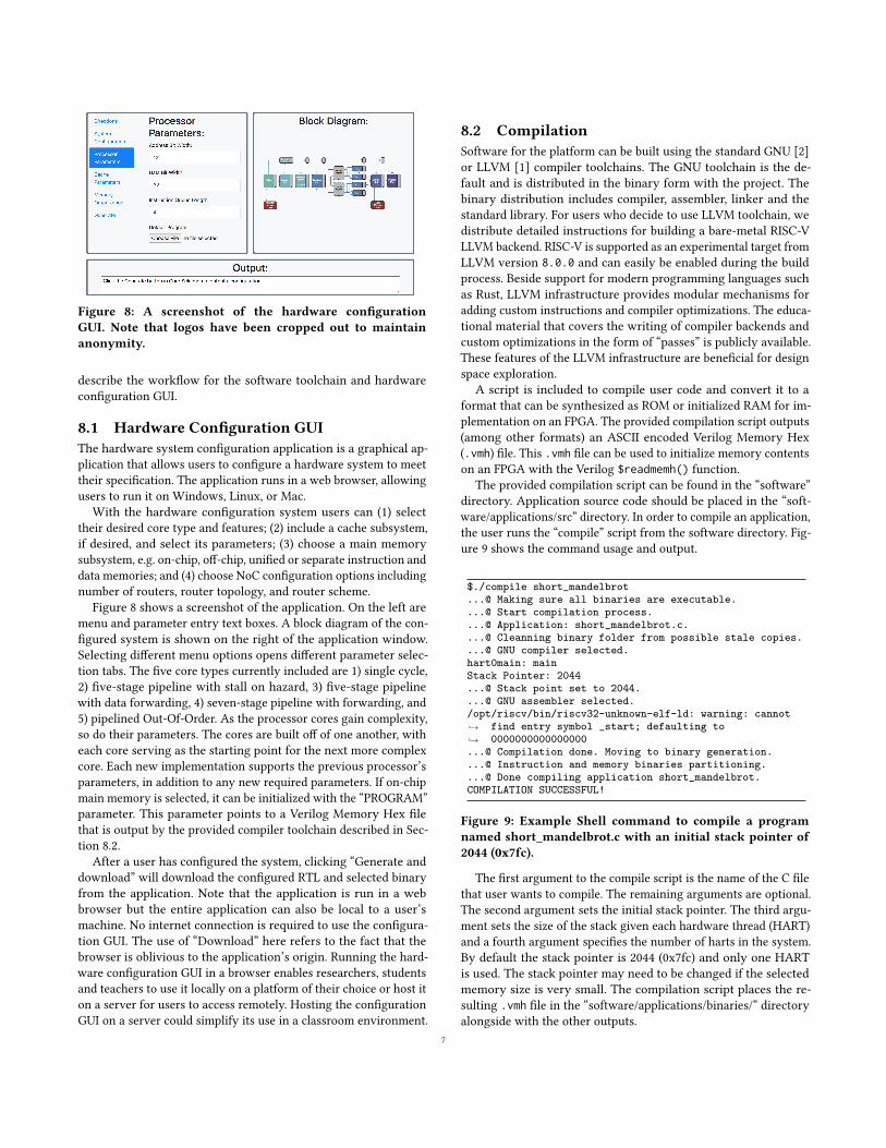
Figure 8: A screenshot of the hardware configurationGUI. Note that logos have been cropped out to maintainanonymity.
describe the workflow for the software toolchain and hardwareconfiguration GUI.
8.1 Hardware Configuration GUIThe hardware system configuration application is a graphical ap-plication that allows users to configure a hardware system to meettheir specification. The application runs in a web browser, allowingusers to run it on Windows, Linux, or Mac.
With the hardware configuration system users can (1) selecttheir desired core type and features; (2) include a cache subsystem,if desired, and select its parameters; (3) choose a main memorysubsystem, e.g. on-chip, off-chip, unified or separate instruction anddata memories; and (4) choose NoC configuration options includingnumber of routers, router topology, and router scheme.
Figure 8 shows a screenshot of the application. On the left aremenu and parameter entry text boxes. A block diagram of the con-figured system is shown on the right of the application window.Selecting different menu options opens different parameter selec-tion tabs. The five core types currently included are 1) single cycle,2) five-stage pipeline with stall on hazard, 3) five-stage pipelinewith data forwarding, 4) seven-stage pipeline with forwarding, and5) pipelined Out-Of-Order. As the processor cores gain complexity,so do their parameters. The cores are built off of one another, witheach core serving as the starting point for the next more complexcore. Each new implementation supports the previous processor’sparameters, in addition to any new required parameters. If on-chipmain memory is selected, it can be initialized with the “PROGRAM”parameter. This parameter points to a Verilog Memory Hex filethat is output by the provided compiler toolchain described in Sec-tion 8.2.
After a user has configured the system, clicking “Generate anddownload” will download the configured RTL and selected binaryfrom the application. Note that the application is run in a webbrowser but the entire application can also be local to a user’smachine. No internet connection is required to use the configura-tion GUI. The use of “Download” here refers to the fact that thebrowser is oblivious to the application’s origin. Running the hard-ware configuration GUI in a browser enables researchers, studentsand teachers to use it locally on a platform of their choice or host iton a server for users to access remotely. Hosting the configurationGUI on a server could simplify its use in a classroom environment.
8.2 CompilationSoftware for the platform can be built using the standard GNU [2]or LLVM [1] compiler toolchains. The GNU toolchain is the de-fault and is distributed in the binary form with the project. Thebinary distribution includes compiler, assembler, linker and thestandard library. For users who decide to use LLVM toolchain, wedistribute detailed instructions for building a bare-metal RISC-VLLVM backend. RISC-V is supported as an experimental target fromLLVM version 8.0.0 and can easily be enabled during the buildprocess. Beside support for modern programming languages suchas Rust, LLVM infrastructure provides modular mechanisms foradding custom instructions and compiler optimizations. The educa-tional material that covers the writing of compiler backends andcustom optimizations in the form of “passes” is publicly available.These features of the LLVM infrastructure are beneficial for designspace exploration.
A script is included to compile user code and convert it to aformat that can be synthesized as ROM or initialized RAM for im-plementation on an FPGA. The provided compilation script outputs(among other formats) an ASCII encoded Verilog Memory Hex(.vmh) file. This .vmh file can be used to initialize memory contentson an FPGA with the Verilog $readmemh() function.
The provided compilation script can be found in the “software”directory. Application source code should be placed in the “soft-ware/applications/src” directory. In order to compile an application,the user runs the “compile” script from the software directory. Fig-ure 9 shows the command usage and output.
metal RISC-V LLVM backend. RISC-V is supportedas an experimental target from LLVM version 8.0.0and can easily be enabled during the build process. Be-side support for modern programming languages suchas Rust, LLVM infrastructure provides modular mech-anisms for adding custom instructions and compiler op-timizations. The educational material that covers thewriting of compiler backends and custom optimizationsin the form of “passes” is publicly available. These fea-tures of the LLVM infrastructure are beneficial for de-sign space exploration.A script is included to compile user code and con-
vert it to a format that can be synthesized as ROM orinitialized RAM for implementation on an FPGA. Theprovided compilation script outputs (among other for-mats) an ASCII encoded Verilog Memory Hex (.vmh)file. This .vmh file can be used to initialize memorycontents on an FPGA with the Verilog $readmemh()function.The provided compilation script can be found in the
“software” directory. Application source code shouldbe placed in the “software/applications/src” directory.In order to compile an application, the user runs the“compile” script from the software directory. Figure 8shows the command usage and output.
$./compile short_mandelbrot...@ Making sure all binaries are executable....@ Start compilation process....@ Application: short_mandelbrot.c....@ Cleanning binary folder from possible stale copies....@ GNU compiler selected.hart0main: mainStack Pointer: 2044...@ Stack point set to 2044....@ GNU assembler selected./opt/riscv/bin/riscv32-unknown-elf-ld: warning: cannot
find entry symbol _start; defaulting to0000000000000000
↪→↪→...@ Compilation done. Moving to binary generation....@ Instruction and memory binaries partitioning....@ Done compiling application short_mandelbrot.COMPILATION SUCCESSFUL!
Figure 8: Example Shell command to compilea program named short mandelbrot.c with aninitial stack pointer of 2044 (0x7fc).
The first argument to the compile script is the nameof the C file that user wants to compile. The remain-ing arguments are optional. The second argument setsthe initial stack pointer. The third argument sets thesize of the stack given each hardware thread (HART)and a fourth argument specifies the number of hartsin the system. By default the stack pointer is 2044(0x7fc) and only one HART is used. The stack pointermay need to be changed if the selected memory size isvery small. The compilation script places the resulting.vmh file in the “software/applications/binaries/” direc-tory alongside with the other outputs.The project currently does not support any operat-
ing system and applications must be run in a bare-metalenvironment. To eliminate any extra setup by the user
(a) (b)
Figure 9: Incorrectly (a) and correctly (b) ren-dered Mandelbrot set.
to enable bare-metal execution of their code, the com-piler script wraps the user application with assemblycode to initialize each of the registers and call the mainfunction. The assembly wrapper executes an infiniteloop after the main function returns. This wrapper canbe thought of as a simple kernel. Multiple HARTs canbe used by writing a function named hartN_main() foreach HART, where “N” is the HART number. The sim-ple kernel will call each HART’s main function.The user’s custom compiler choice as well as the com-
piler options should be provided as environment vari-ables. The environment variable used to supply addi-tional options to GCC compiler is “GCC OPTS”. Thevariables to control the version of LLVM compiler andthe additional options are“LLVM”and“LLVM OPTS”,respectively. The user should provide these options be-fore they run the compilation script. That being so, wemaintain the flexibility of the compilation process andsupport the standard tools for code optimizations.After running the provided compile script, a user can
set the “PROGRAM” parameter to the path of their.vmh file (manually or in the hardware configurationGUI) and synthesize their design. The instruction mem-ory of the processor will be initialized with the contentsof the binary if it is on-chip. The instruction memoryalso has a port for writing new programs after the de-sign has been configured on an FPGA.
9. PLATFORM EVALUATION
9.1 The Platform as a Teaching ToolThe different versions of the processing cores in this
platform lay the groundwork for a hands-on educationin micro-architecture design. The cores included in thisplatform provide various levels of complexity for usersto build on.In order to evaluate the ease of use of the platform,
students used it as a baseline in their design space explo-ration and added peripheral devices such as a memorymapped VGA frame buffer. This frame buffer was usedto render a Mandelbrot fractal. Testing the renderingprogram revealed that the original test suite did notprovide full coverage of the instruction set and some in-structions did not execute correctly. After troubleshoot-ing, it was found that the hardware system’s ALU didnot correctly execute signed operations. Figure 9 com-pares the incorrect rendering with the correct rendering.Finding and fixing this bug is an example of how thisdesign space exploration platform enables users to make
Figure 9: Example Shell command to compile a programnamed short_mandelbrot.c with an initial stack pointer of2044 (0x7fc).
The first argument to the compile script is the name of the C filethat user wants to compile. The remaining arguments are optional.The second argument sets the initial stack pointer. The third argu-ment sets the size of the stack given each hardware thread (HART)and a fourth argument specifies the number of harts in the system.By default the stack pointer is 2044 (0x7fc) and only one HARTis used. The stack pointer may need to be changed if the selectedmemory size is very small. The compilation script places the re-sulting .vmh file in the “software/applications/binaries/” directoryalongside with the other outputs.
7
(a) (b)
Figure 10: Incorrectly (a) and correctly (b) rendered Mandel-brot set.
The project currently does not support any operating system andapplications must be run in a bare-metal environment. To eliminateany extra setup by the user to enable bare-metal execution of theircode, the compiler script wraps the user application with assemblycode to initialize each of the registers and call themain function. Theassembly wrapper executes an infinite loop after the main functionreturns. This wrapper can be thought of as a simple kernel. MultipleHARTs can be used by writing a function named hartN_main()for each HART, where “N” is the HART number. The simple kernelwill call each HART’s main function.
The user’s custom compiler choice as well as the compiler op-tions should be provided as environment variables. The environ-ment variable used to supply additional options to GCC compileris “GCC_OPTS”. The variables to control the version of LLVM com-piler and the additional options are “LLVM” and “LLVM_OPTS”,respectively. The user should provide these options before they runthe compilation script. That being so, we maintain the flexibilityof the compilation process and support the standard tools for codeoptimizations.
After running the provided compile script, a user can set the“PROGRAM” parameter to the path of their .vmh file (manually orin the hardware configuration GUI) and synthesize their design.The instruction memory of the processor will be initialized withthe contents of the binary if it is on-chip. The instruction memoryalso has a port for writing new programs after the design has beenconfigured on an FPGA.
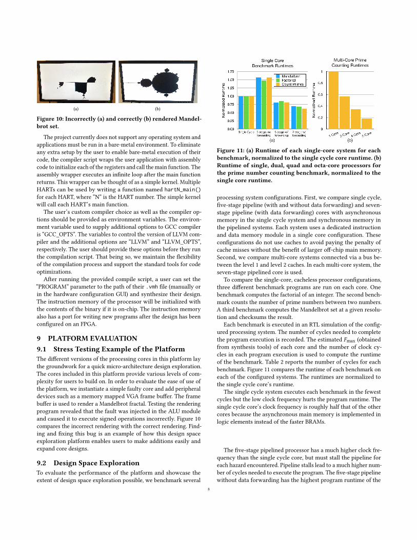
9 PLATFORM EVALUATION9.1 Stress Testing Example of the PlatformThe different versions of the processing cores in this platform laythe groundwork for a quick micro-architecture design exploration.The cores included in this platform provide various levels of com-plexity for users to build on. In order to evaluate the ease of use ofthe platform, we instantiate a simple faulty core and add peripheraldevices such as a memory mapped VGA frame buffer. The framebuffer is used to render a Mandelbrot fractal. Testing the renderingprogram revealed that the fault was injected in the ALU moduleand caused it to execute signed operations incorrectly. Figure 10compares the incorrect rendering with the correct rendering. Find-ing and fixing this bug is an example of how this design spaceexploration platform enables users to make additions easily andexpand core designs.
9.2 Design Space ExplorationTo evaluate the performance of the platform and showcase theextent of design space exploration possible, we benchmark several
Figure 11: (a) Runtime of each single-core system for eachbenchmark, normalized to the single cycle core runtime. (b)Runtime of single, dual, quad and octa-core processors forthe prime number counting benchmark, normalized to thesingle core runtime.
processing system configurations. First, we compare single cycle,five-stage pipeline (with and without data forwarding) and seven-stage pipeline (with data forwarding) cores with asynchronousmemory in the single cycle system and synchronous memory inthe pipelined systems. Each system uses a dedicated instructionand data memory module in a single core configuration. Theseconfigurations do not use caches to avoid paying the penalty ofcache misses without the benefit of larger off-chip main memory.Second, we compare multi-core systems connected via a bus be-tween the level 1 and level 2 caches. In each multi-core system, theseven-stage pipelined core is used.
To compare the single-core, cacheless processor configurations,three different benchmark programs are run on each core. Onebenchmark computes the factorial of an integer. The second bench-mark counts the number of prime numbers between two numbers.A third benchmark computes the Mandelbrot set at a given resolu-tion and checksums the result.
Each benchmark is executed in an RTL simulation of the config-ured processing system. The number of cycles needed to completethe program execution is recorded. The estimated Fmax (obtainedfrom synthesis tools) of each core and the number of clock cy-cles in each program execution is used to compute the runtimeof the benchmark. Table 2 reports the number of cycles for eachbenchmark. Figure 11 compares the runtime of each benchmark oneach of the configured systems. The runtimes are normalized tothe single cycle core’s runtime.
The single cycle system executes each benchmark in the fewestcycles but the low clock frequency hurts the program runtime. Thesingle cycle core’s clock frequency is roughly half that of the othercores because the asynchronous main memory is implemented inlogic elements instead of the faster BRAMs.
The five-stage pipelined processor has a much higher clock fre-quency than the single cycle core, but must stall the pipeline foreach hazard encountered. Pipeline stalls lead to a much higher num-ber of cycles needed to execute the program. The five-stage pipelinewithout data forwarding has the highest program runtime of the
8
tested cores. Adding data forwarding to the five-stage pipeline cutsthe program runtime in half, yielding runtimes better than thesingle cycle core.
The seven-stage pipeline adds two stages to the five-stage pipelineto support synchronous memories without inserting NOPs. Theseextra stages increase the clock frequency but also increase the num-ber of cycles needed to compute the target address of branch andjump instructions. The five-stage pipeline must wait two cyclesbefore a jump or branch address is ready while the seven-stagepipeline must wait three cycles. Neither pipeline has a branchpredictor. The extra cycles spent stalling are canceled out by thehigher clock frequency of the seven-stage pipeline. The seven-stagepipeline has the best runtime for each benchmark.
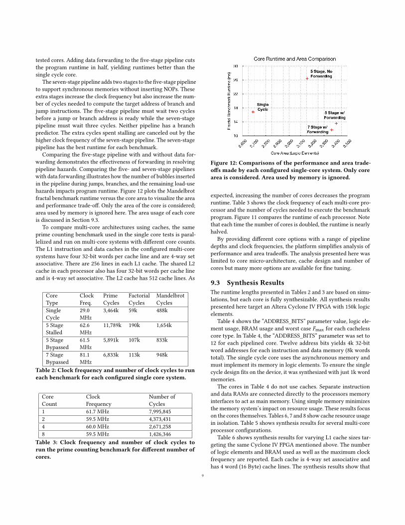
Comparing the five-stage pipeline with and without data for-warding demonstrates the effectiveness of forwarding in resolvingpipeline hazards. Comparing the five- and seven-stage pipelineswith data forwarding illustrates how the number of bubbles insertedin the pipeline during jumps, branches, and the remaining load-usehazards impacts program runtime. Figure 12 plots the Mandelbrotfractal benchmark runtime versus the core area to visualize the areaand performance trade-off. Only the area of the core is considered;area used by memory is ignored here. The area usage of each coreis discussed in Section 9.3.
To compare multi-core architectures using caches, the sameprime counting benchmark used in the single core tests is paral-lelized and run on multi-core systems with different core counts.The L1 instruction and data caches in the configured multi-coresystems have four 32-bit words per cache line and are 4-way setassociative. There are 256 lines in each L1 cache. The shared L2cache in each processor also has four 32-bit words per cache lineand is 4-way set associative. The L2 cache has 512 cache lines. As
Core Clock Prime Factorial MandelbrotType Freq. Cycles Cycles CyclesSingleCycle
29.0MHz
3,464k 59k 488k
5 StageStalled
62.6MHz
11,789k 190k 1,654k
5 StageBypassed
61.5MHz
5,891k 107k 833k
7 StageBypassed
81.1MHz
6,833k 113k 948k
Table 2: Clock frequency and number of clock cycles to runeach benchmark for each configured single core system.
Core Clock Number ofCount Frequency Cycles1 61.7 MHz 7,995,8452 59.5 MHz 4,373,4314 60.0 MHz 2,671,2588 59.5 MHz 1,426,346
Table 3: Clock frequency and number of clock cycles torun the prime counting benchmark for different number ofcores.
Figure 12: Comparisons of the performance and area trade-offs made by each configured single-core system. Only corearea is considered. Area used by memory is ignored.
expected, increasing the number of cores decreases the programruntime. Table 3 shows the clock frequency of each multi-core pro-cessor and the number of cycles needed to execute the benchmarkprogram. Figure 11 compares the runtime of each processor. Notethat each time the number of cores is doubled, the runtime is nearlyhalved.
By providing different core options with a range of pipelinedepths and clock frequencies, the platform simplifies analysis ofperformance and area tradeoffs. The analysis presented here waslimited to core micro-architecture, cache design and number ofcores but many more options are available for fine tuning.
9.3 Synthesis ResultsThe runtime lengths presented in Tables 2 and 3 are based on simu-lations, but each core is fully synthesizable. All synthesis resultspresented here target an Altera Cyclone IV FPGA with 150k logicelements.
Table 4 shows the “ADDRESS_BITS” parameter value, logic ele-ment usage, BRAM usage and worst case Fmax for each cachelesscore type. In Table 4, the “ADDRESS_BITS” parameter was set to12 for each pipelined core. Twelve address bits yields 4k 32-bitword addresses for each instruction and data memory (8k wordstotal). The single cycle core uses the asynchronous memory andmust implement its memory in logic elements. To ensure the singlecycle design fits on the device, it was synthesized with just 1k wordmemories.
The cores in Table 4 do not use caches. Separate instructionand data RAMs are connected directly to the processors memoryinterfaces to act as main memory. Using simple memory minimizesthe memory system’s impact on resource usage. These results focuson the cores themselves. Tables 6, 7 and 8 show cache resource usagein isolation. Table 5 shows synthesis results for several multi-coreprocessor configurations.
Table 6 shows synthesis results for varying L1 cache sizes tar-geting the same Cyclone IV FPGA mentioned above. The numberof logic elements and BRAM used as well as the maximum clockfrequency are reported. Each cache is 4-way set associative andhas 4 word (16 Byte) cache lines. The synthesis results show that
9
varying the cache size while maintaining the same line size andassociativity only marginally changes the logic element usage andFmax. Only the BRAM usage is significantly impacted by cache size.
Table 7 shows synthesis results for 4kB L1 caches with 4 word(16 Byte), cache lines and various associativities. Intuitively, thenumber of logic elements grows with the associativity while Fmaxshrinks. The BRAM usage grows slowly with the associativity. The16-way associative cache uses 2k more BRAM bits than the 1-way(direct mapped) cache. The increase in BRAM usage with higherassociativities can be explained by the higher BRAM usage in the‘replacement_controller’ module, which implements the true leastrecently used (LRU) replacement policy.
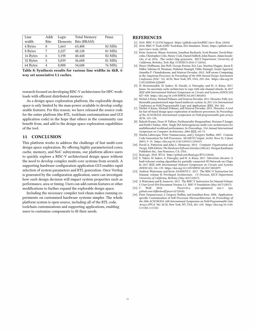
Table 8 shows synthesis results for 4kB L1 cacheswith linewidthsranging from 1 word (4 Bytes) to 16 words (64 Bytes). Varying theline width trades off BRAM and logic elements. Smaller line widthsuse more BRAM bits for tag storage, while larger line widths usemore logic elements to implement registers and buses to handlewider cache lines.
Table 5 shows the resource usage for processors with 1, 2, 4 and8 cores. The cores used in the multi-core processor are versionsof the 7-stage pipelined core. The L1 caches, shared L2 cache, andcoherence controller modules add a significant area overhead butenable the use of complex memory hierarchies. The significantlylarger BRAM usage in the multi-core processors stems from thelarge cache and on-chip main memory. The memory in the singlecore processors was made to be smaller because larger memorieswere not needed for the benchmarks. Note that the BRAM usage forthe 8-core processor is slightly greater than what is available on thedevice. We have included the results here because moving the mainmemory to off-chip SRAM available on our development boardwould allow the caches to fit within the device BRAM withoutsignificantly impacting the performance.
The memory hierarchy for each of the processors in Table 5 usesthe same parameters. 16kB L1 caches, 32kB L2 caches and a mainmemory of 256kB.
The different cores and cache configurations supported by theplatform enable users to examine the difference between designchoices quickly. Additional configuration options, including NoCrouting, NoC topology, and on/off-chip main memory configura-tions have not been included here due to space restrictions.
Each core builds off of the same set of base modules, makingit easy to integrate experimental features into several of them bymodifying only the base module. This extensibility opens up evenmore possibilities for design space exploration. We have used thistechnique to add data forwarding, originally added to the five-stagepipeline, to the out-of-order and seven-stage pipeline cores.
10 FUTUREWORKThe goal of this work is to explore techniques to develop a fast,flexible, multi-core design space exploration platform, enablingusers to understand the impact of their design decisions and quicklytest different configurations. To expand the number of configurationoptions available to users further, the authors plan to add severalnew features to the available cores, including branch predictors,
Core Addr Logic BRAM FmaxType Bits Elements BitsSingleCycle
10 53,448 0 29.0MHz
5 StageStalled
12 3,160 262,144 62.6MHz
5 StageBypassed
12 3,406 262,144 61.5MHz
7 StageBypassed
12 3,366 262,144 81.1MHz
Table 4: Synthesis results for each configured single-coreprocessing system.
Core Logic Total Memory FmaxCount Elements Bits (BRAM) Fmax1 12,206 2,736,128 61.7 MHz2 21,123 3,055,616 59.5 MHz4 38,921 3,694,592 60.0 MHz8 83,020 4,972,544 59.5 MHz
Table 5: Synthesis results for each configuredmulti-core pro-cessing system.
Cache Addr Logic Total Memory FmaxSize Bits Elements Bits (BRAM)1kB 4 3,208 10,240 79.1 MHz2kB 5 3,196 20,352 81.0 MHz4kB 6 3,198 40,448 82.6 MHz8kB 7 3,189 80,384 81.1 MHz16kB 8 3,189 159,744 82.8 MHz
Table 6: Synthesis results for various sizes of 4-way set as-sociative L1 caches. Each cacheline is 16 Bytes (four 32-bitwords)
Cache Addr Logic Total Memory FmaxWays Bits Elements Bits (BRAM)1 8 2,387 39,424 104 MHz2 7 2,736 39,936 97 MHz4 6 3,198 40,448 82 MHz8 5 4,534 40,960 66 MHz16 4 6,546 41,472 49 MHz
Table 7: Synthesis results for various associativities in 4kBL1 caches. Each cacheline is 16 Bytes (four 32-bit words)
hardware multi-threading, and other RISC-V ISA extensions, suchas the floating point (RV32F) or multiply (RV32M) extensions. Eachof these new features will be made available as an option for a user’sdesired core and incorporated into the hardware configuration GUI.
The platform has already supported, and will continue to sup-port, research relating to secure architectures focused on enablingefficient obfuscation with hardware-software co-design. The im-provements described above will be necessary to support additional
10
Line Addr Logic Total Memory Fmaxwidth Bits Elements Bits (BRAM)4 Bytes 8 1,663 63,488 82 MHz8 Bytes 7 2,227 48,128 81 MHz16 Bytes 6 3,198 40,448 82 MHz32 Bytes 5 5,039 36,608 81 MHz64 Bytes 4 8,888 34,688 76 MHz
Table 8: Synthesis results for various line widths in 4kB, 4-way set associative L1 caches.
research focused on developing RISC-V architectures for HPCwork-loads with efficient distributed memory.
As a design space exploration platform, the explorable designspace is only limited by the man-power available to develop config-urable features. For this reason, we have released the source codefor the entire platform (the RTL, toolchain customizations and GUIapplication code) in the hope that others in the community canbenefit from, and add to the design space exploration capabilitiesof the tool.
11 CONCLUSIONThis platform works to address the challenge of fast multi-coredesign space exploration. By offering highly parameterized cores,cache, memory, and NoC subsystems, our platform allows usersto quickly explore a RISC-V architectural design space withoutthe need to develop complex multi-core systems from scratch. Asupporting hardware configuration application GUI enables rapidselection of system parameters and RTL generation. Once Verilogis generated by the configuration application, users can investigatehow each design decision will impact system properties such asperformance, area or timing. Users can add custom features or othermodifications to further expand the explorable design space.
Including the necessary compiler tool-chain makes running ex-periments on customized hardware systems simpler. The wholeplatform system is open source, including all of the RTL code,toolchain customizations and supporting applications, enablingusers to customize components to fit their needs.
REFERENCES[1] 2018. RISC-V LLVM Support. https://github.com/lowRISC/riscv-llvm. (2018).[2] 2018. RISC-V Tools (GNU Toolchain, ISA Simulator, Tests). https://github.com/
riscv/riscv-tools. (2018).[3] Krste Asanovic, Rimas Avizienis, Jonathan Bachrach, Scott Beamer, David Bian-
colin, Christopher Celio, Henry Cook, Daniel Dabbelt, John Hauser, Adam Izraele-vitz, et al. 2016. The rocket chip generator. EECS Department, University ofCalifornia, Berkeley, Tech. Rep. UCB/EECS-2016-17 (2016).
[4] Henry Hoffmann, Jim Holt, George Kurian, Eric Lau, Martina Maggio, Jason E.Miller, Sabrina M. Neuman, Mahmut Sinangil, Yildiz Sinangil, Anant Agarwal,Anantha P. Chandrakasan, and Srinivas Devadas. 2012. Self-aware Computingin the Angstrom Processor. In Proceedings of the 49th Annual Design AutomationConference (DAC ’12). ACM, New York, NY, USA, 259–264. https://doi.org/10.1145/2228360.2228409
[5] H. Hosseinzadeh, M. Isakov, M. Darabi, A. Patooghy, and M. A. Kinsy. 2017.Janus: An uncertain cache architecture to cope with side channel attacks. In 2017IEEE 60th International Midwest Symposium on Circuits and Systems (MWSCAS).827–830. https://doi.org/10.1109/MWSCAS.2017.8053051
[6] Michel A Kinsy, Michael Pellauer, and Srinivas Devadas. 2011. Heracles: Fully syn-thesizable parameterized mips-based multicore system. In 2011 21st InternationalConference on Field Programmable Logic and Applications. IEEE, 356–362.
[7] Michel A Kinsy, Michael Pellauer, and Srinivas Devadas. 2013. Heracles: A toolfor fast rtl-based design space exploration of multicore processors. In Proceedingsof the ACM/SIGDA international symposium on Field programmable gate arrays.ACM, 125–134.
[8] Rakesh Kumar, Dean M Tullsen, Parthasarathy Ranganathan, Norman P Jouppi,and Keith I Farkas. 2004. Single-ISA heterogeneous multi-core architectures formultithreaded workload performance. In Proceedings. 31st Annual InternationalSymposium on Computer Architecture, 2004. IEEE, 64–75.
[9] Martin Labrecque, Peter Yiannacouras, and J. Gregory Steffan. 2007. CustomCode Generation for Soft Processors. SIGARCH Comput. Archit. News 35, 3 (June2007), 9–19. https://doi.org/10.1145/1294313.1294319
[10] David A. Patterson and John L. Hennessy. 2013. Computer Organization andDesign, Fifth Edition: The Hardware/Software Interface (5th ed.). Morgan KaufmannPublishers Inc., San Francisco, CA, USA.
[11] RoaLogic. 2018. RV12. https://github.com/RoaLogic/RV12 (2018).[12] E. Taheri, M. Isakov, A. Patooghy, and M. A. Kinsy. 2017. Advertiser elevator: A
fault tolerant routing algorithm for partially connected 3D Network-on-Chips.In 2017 IEEE 60th International Midwest Symposium on Circuits and Systems(MWSCAS). 136–139. https://doi.org/10.1109/MWSCAS.2017.8052879
[13] Andrew Waterman and Krste ASANOVI C. 2017. The RISC-V Instruction SetManual, volume II: Privileged Architecture. CS Division, EECE Department,University of California, Berkeley (May 2017) (2017).
[14] A Waterman and K Asanovic. 2017. The RISC-V Instruction Set Manual-VolumeI: User-Level ISA-Document Version 2.2. RISC-V Foundation (May 2017) (2017).
[15] C Wolf. 2018. Picorv32-a size-optimized risc-v cpu.github.com/cliffordwolf/picorv32 (2018).
[16] Peter Yiannacouras, J. Gregory Steffan, and Jonathan Rose. 2006. Application-specific Customization of Soft Processor Microarchitecture. In Proceedings ofthe 2006 ACM/SIGDA 14th International Symposium on Field Programmable GateArrays (FPGA ’06). ACM, New York, NY, USA, 201–210. https://doi.org/10.1145/1117201.1117231
11