Embed Size (px)
Citation preview

Application ReportSCLA015 - February 2001
1
Bus-Hold CircuitEilhard Haseloff Standard Linear & Logic
ABSTRACT
When designing systems that include CMOS devices, designers must pay special attentionto the operating condition in which all of the bus drivers are in an inactive, high-impedancecondition (3-state). Unless special measures are taken, this condition can lead to undefinedlevels and, thus, to a significant increase in the device’s power dissipation. In extreme cases,this leads to oscillation of the affected components, which has a negative effect on both thereliability – in terms of both functioning and lifetime – and the electromagnetic compatibilityof the entire system. This application report addresses a range of circuit design features thatminimize these problems. The main purpose of this application report is to present a novelbus-hold circuit that TI has integrated into a wide range of modern bus-interface devices.This bus-hold circuit is the ideal way of meeting the demands discussed here, thus helpingto ensure the functional reliability of a system.
Contents
1 Introduction 3. . . . . . . . . . . . . . . . . . . . . . . . . . . . . . . . . . . . . . . . . . . . . . . . . . . . . . . . . . . . . . . . . . . . . . . . .
2 Behavior of CMOS Input Stages 3. . . . . . . . . . . . . . . . . . . . . . . . . . . . . . . . . . . . . . . . . . . . . . . . . . . . . .
3 Problems Posed by Bus Systems 6. . . . . . . . . . . . . . . . . . . . . . . . . . . . . . . . . . . . . . . . . . . . . . . . . . . . .
4 Avoidance of Undefined Levels in Bus Systems 7. . . . . . . . . . . . . . . . . . . . . . . . . . . . . . . . . . . . . . . 4.1 Avoidance of Undefined Levels Via Appropriate Bus Control 7. . . . . . . . . . . . . . . . . . . . . . . . . . . 4.2 Pullup Resistors 8. . . . . . . . . . . . . . . . . . . . . . . . . . . . . . . . . . . . . . . . . . . . . . . . . . . . . . . . . . . . . . . . . . 4.3 Bus-Hold Circuit 9. . . . . . . . . . . . . . . . . . . . . . . . . . . . . . . . . . . . . . . . . . . . . . . . . . . . . . . . . . . . . . . . . .
5 Integrated Bus-Hold Circuit 10. . . . . . . . . . . . . . . . . . . . . . . . . . . . . . . . . . . . . . . . . . . . . . . . . . . . . . . . . .
6 Application Information 12. . . . . . . . . . . . . . . . . . . . . . . . . . . . . . . . . . . . . . . . . . . . . . . . . . . . . . . . . . . . . 6.1 Additional Load Caused by Bus-Hold Circuits 12. . . . . . . . . . . . . . . . . . . . . . . . . . . . . . . . . . . . . . . 6.2 Influence on the Circuit’s Power Loss 13. . . . . . . . . . . . . . . . . . . . . . . . . . . . . . . . . . . . . . . . . . . . . . 6.3 Presetting Logic Levels 14. . . . . . . . . . . . . . . . . . . . . . . . . . . . . . . . . . . . . . . . . . . . . . . . . . . . . . . . . . .
7 Summary 15. . . . . . . . . . . . . . . . . . . . . . . . . . . . . . . . . . . . . . . . . . . . . . . . . . . . . . . . . . . . . . . . . . . . . . . . . . .
TI is a trademark of Texas Instruments.

SCLA015
2 Bus-Hold Circuit
List of Figures
1 Input Stage of a CMOS Circuit 3. . . . . . . . . . . . . . . . . . . . . . . . . . . . . . . . . . . . . . . . . . . . . . . . . . . . . . . . . . 2 Power Consumption of CMOS Input Stages in Relation to Input Voltage 4. . . . . . . . . . . . . . . . . . . . . . 3 Parasitic Components Causing Circuit Oscillation 4. . . . . . . . . . . . . . . . . . . . . . . . . . . . . . . . . . . . . . . . . 4 Oscillation at the Output of a CMOS Circuit Whose Input Is Triggered
by a Signal With a Rise Time of tr = 200 ns 5. . . . . . . . . . . . . . . . . . . . . . . . . . . . . . . . . . . . . . . . . . . . . . . 5 Unidirectional Transmission Line 6. . . . . . . . . . . . . . . . . . . . . . . . . . . . . . . . . . . . . . . . . . . . . . . . . . . . . . . . 6 Bidirectional Transmission Line of a Bus System 6. . . . . . . . . . . . . . . . . . . . . . . . . . . . . . . . . . . . . . . . . . 7 Creating a Defined Level Using Pullup Resistors 8. . . . . . . . . . . . . . . . . . . . . . . . . . . . . . . . . . . . . . . . . . 8 Bus With Bus-Hold Circuit 9. . . . . . . . . . . . . . . . . . . . . . . . . . . . . . . . . . . . . . . . . . . . . . . . . . . . . . . . . . . . . . 9 Simplified Circuit Diagram of Bus-Hold Circuits 10. . . . . . . . . . . . . . . . . . . . . . . . . . . . . . . . . . . . . . . . . . 10 Characteristic Input Curve of Bus-Interface Devices With the Bus-Hold Function 11. . . . . . . . . . . . . 11 A Simple Bus System 12. . . . . . . . . . . . . . . . . . . . . . . . . . . . . . . . . . . . . . . . . . . . . . . . . . . . . . . . . . . . . . . .
List of Tables
1 Specifications of the 3-State Outputs With Bus Hold, SN74LVCH245 12. . . . . . . . . . . . . . . . . . . . . . . 2 Specifications of the 3-State Outputs, SN74AHC245 12. . . . . . . . . . . . . . . . . . . . . . . . . . . . . . . . . . . . . 3 Specifications of the 3-State Outputs, TMS320C6201 13. . . . . . . . . . . . . . . . . . . . . . . . . . . . . . . . . . . . .
SCLA015
3 Bus-Hold Circuit
1 Introduction
In recent years, CMOS technology has become the technology of choice for development andsubsequent production of highly integrated (VLSI) circuits because of the high complexity andlow power consumption that can be achieved with these types of circuits. Also, the technologyhas proved itself with less complex devices, such as the SN74AHC and SN74AC logic families,as well as with the SN74LVC and SN74ALVC logic families developed for use with lower supplyvoltages. Furthermore, it is possible for important parameters, such as propagation delay timeand drive capability, to achieve properties similar to those found in the bipolar circuits thatpreviously dominated this field. In this respect, the particularly powerful SN74ABT and SN74LVTBiCMOS devices, which combine the strengths of CMOS circuits (low power consumption) withthose of bipolar circuits (lower propagation delay time and greater drive capability), deservemention.
When using these integrated CMOS and BiCMOS devices, the designer also must considercertain properties of these devices that the specification sheets deal with only briefly, if at all.This includes, for example, the behavior of the input stages of these components when nodefined logic level is established.
2 Behavior of CMOS Input Stages
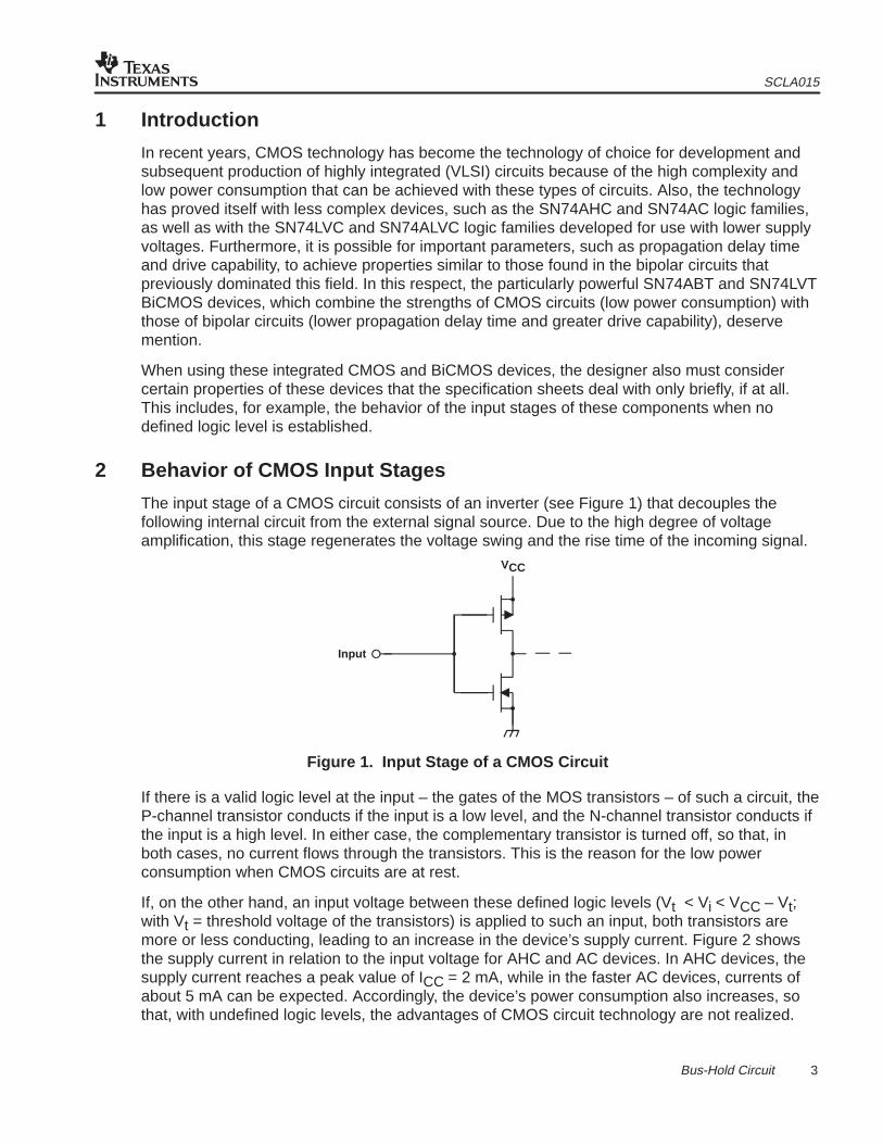
The input stage of a CMOS circuit consists of an inverter (see Figure 1) that decouples thefollowing internal circuit from the external signal source. Due to the high degree of voltageamplification, this stage regenerates the voltage swing and the rise time of the incoming signal.
VCC
Input
Figure 1. Input Stage of a CMOS Circuit
If there is a valid logic level at the input – the gates of the MOS transistors – of such a circuit, theP-channel transistor conducts if the input is a low level, and the N-channel transistor conducts ifthe input is a high level. In either case, the complementary transistor is turned off, so that, inboth cases, no current flows through the transistors. This is the reason for the low powerconsumption when CMOS circuits are at rest.
If, on the other hand, an input voltage between these defined logic levels (Vt < Vi < VCC – Vt;with Vt = threshold voltage of the transistors) is applied to such an input, both transistors aremore or less conducting, leading to an increase in the device’s supply current. Figure 2 showsthe supply current in relation to the input voltage for AHC and AC devices. In AHC devices, thesupply current reaches a peak value of ICC = 2 mA, while in the faster AC devices, currents ofabout 5 mA can be expected. Accordingly, the device’s power consumption also increases, sothat, with undefined logic levels, the advantages of CMOS circuit technology are not realized.

SCLA015
4 Bus-Hold Circuit
AC
AHC
VCC = 5 V
5
4
3
2
1
0543210
I
VI – V
CC
– m
A
Figure 2. Power Consumption of CMOS Input Stages vs Input Voltage
The effects shown in Figure 2 are typical of all CMOS circuits. Accordingly, this phenomenonalso must be taken into account when dealing with VLSI circuits, such as microprocessors ormemory devices.
Furthermore, CMOS device data sheets recommend the slowest possible rise time for the inputsignal to ensure optimum functioning of components. However, slowly rising edges cause fastintegrated circuits to malfunction and can, in extreme cases, lead to destruction of the circuit.Figure 3 shows an inverting buffer stage with the parasitic inductances of the package leads (LP)and the capacitive load (CL) at the output. If, for example, the input voltage of this kind of circuitrises from low to high, and reaches the threshold voltage, the output switches abruptly from highto low due to the high voltage gain, and discharges CL. The discharge current causes a voltagedrop at the package inductance of the ground terminal, which raises the internal ground potentialof the integrated circuit, meaning that the voltage difference between the input and the internalground potential decreases, giving the appearance of a decrease of the input voltage. If, due totoo slow a slew rate, in the meantime, the input voltage has not risen sufficiently, the input stageswitches to the opposite state, and the same process repeats, but with the opposite polarity.This process repeats periodically, with the periodicity of the oscillation determined by thedevice’s propagation delay time. In fast logic circuits, the oscillation is above 50 MHz.
LP
LP
VCC
CLLP
Figure 3. Parasitic Components Causing Circuit Oscillation
SCLA015
5 Bus-Hold Circuit
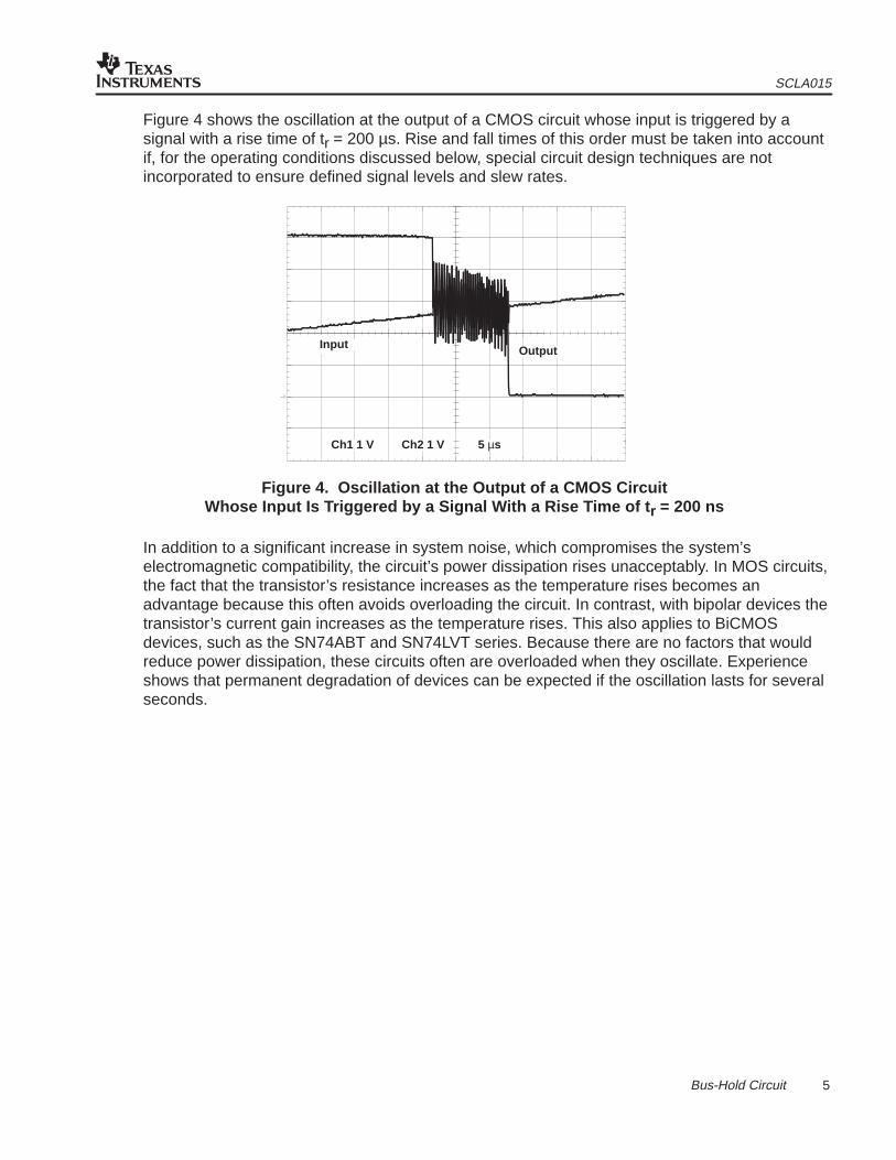
Figure 4 shows the oscillation at the output of a CMOS circuit whose input is triggered by asignal with a rise time of tr = 200 µs. Rise and fall times of this order must be taken into accountif, for the operating conditions discussed below, special circuit design techniques are notincorporated to ensure defined signal levels and slew rates.
Input Output
5 µsCh1 1 V Ch2 1 V
Figure 4. Oscillation at the Output of a CMOS CircuitWhose Input Is Triggered by a Signal With a Rise Time of t r = 200 ns
In addition to a significant increase in system noise, which compromises the system’selectromagnetic compatibility, the circuit’s power dissipation rises unacceptably. In MOS circuits,the fact that the transistor’s resistance increases as the temperature rises becomes anadvantage because this often avoids overloading the circuit. In contrast, with bipolar devices thetransistor’s current gain increases as the temperature rises. This also applies to BiCMOSdevices, such as the SN74ABT and SN74LVT series. Because there are no factors that wouldreduce power dissipation, these circuits often are overloaded when they oscillate. Experienceshows that permanent degradation of devices can be expected if the oscillation lasts for severalseconds.

SCLA015
6 Bus-Hold Circuit
3 Problems Posed by Bus Systems
If only unidirectional transmission lines are involved, the previously mentioned phenomenon ofincreased power dissipation and oscillation can safely be ignored. With unidirectionaltransmission lines there is a driver circuit that always is active at one end of the line, thusensuring defined logic levels (see Figure 5).
Figure 5. Unidirectional Transmission Line
Bus systems (see Figure 6), in which transmission is bidirectional between individual stations,the operating condition in which all of the 3-state output bus drivers are in an inactive,high-impedance state in a 3-state device must be given special attention. Because there is nodriver to impose a defined logic level on the lines, a voltage develops that is determined by theleakage currents of the connected components, thus giving rise to an entirely undefined voltagelevel. In the literature, this state is described as floating inputs. In the case of Widebus circuitswith 16 channels and AC technology, with a supply voltage of VCC = 5 V, the supply current risesto ICC = 16 × 5 mA = 80 mA (see Figure 2). Under this condition, the power consumption of thiscomponent alone increases to 400 mW, which no longer is low power consumption.
Figure 6. Bidirectional Transmission Line of a Bus System
Widebus is a trademark of Texas Instruments.
SCLA015
7 Bus-Hold Circuit
4 Avoidance of Undefined Levels in Bus Systems
4.1 Avoidance of Undefined Levels Via Appropriate Bus Control
A simple way to prevent an undefined logic level in bus systems is to ensure, via appropriatecontrol of the bus, that the duration of the inactive state (3-state) is so short that harmfulvoltages cannot build up. The advantage of this method is that it does not involve any additionalcosts from using special components.
If we first consider a single device and assume that the maximum leakage current, IOZ, of a3-state output in the high-impedance state amounts to 10 µA (see Table 1), and that the inputand output capacitance, CS, of the integrated circuit plus the parasitic capacitance of theconnection lines (which are related to this particular component) amount to about 20 pF, thevoltage on an inactive line drifts away from the defined logic level at a rate that can be calculatedusing equation 1.
dVdt
IOZ
CS
10 A20 pF
0.5 Vs
If a drift away from the logic level of a maximum of 1 V is permitted, so that the supply current ofthe affected input stage has not yet risen too sharply (see Figure 2), the bus may remain in aninactive state (3-state) for a maximum of 2 µs. Usually, more than one device is connected to abus. Where several components are connected to a bus, both their leakage currents and theircapacitances are added, and the time constant calculated in equation 1 does not change.
In the data sheets, semiconductor manufacturers give conservative values for the leakagecurrent, IOZ. When determining these values, the leakage current is measured at an ambienttemperature of TA = 25°C and the maximum values to be expected at operating limits are thencalculated. However, semiconductor physics predicts a doubling of the leakage current when TArises 10°C. Thus, if TA rises from 25°C to 125°C, the leakage current would rise by a factor of210 = 1024. However, this fundamentally correct assumption leads to considerably higher valuesthan are measured in practice. Accordingly, one can assume that typical output leakage currentsare smaller than the specification sheet limits by an order of magnitude, or more.
Another method of avoiding undefined logic levels in inactive buses involves the last activebus-interface device remaining active (monitored by suitable control logic) until another busdriver takes over control of the line. The PCI bus uses this method, whereby inactive bus phasesof any length can be bridged without the extra cost of adding components.
(1)
SCLA015
8 Bus-Hold Circuit
4.2 Pullup Resistors
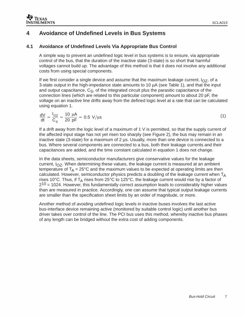
Another way of ensuring a defined level during a bus’s inactive phase is by tying the lines to thesupply voltage or to the ground potential via resistors (Rp in Figure 7). This connection pullsinactive lines to a defined logic level (either high or low).
RPVCC
Figure 7. Creating a Defined Level Using Pullup Resistors
Getting the correct impedance for the resistors is not always easy. The resistors should notsignificantly increase the system’s power dissipation; therefore, high-impedance resistors arerequired (Rp = 10 kΩ to 50 kΩ). The low leakage current of CMOS circuits would permit that.However, it also should be remembered that fast logic circuits need short rise times, tr, at theinputs to avoid unwanted oscillation which, as mentioned previously, can lead to systemmalfunction and, possibly, degradation of components. The desired pullup or pulldownresistance, Rp, can be calculated using equation 2:
Rptr
2.2 Cs n
Where: n = number of devices connected to the line
Modern logic circuits and corresponding VLSI circuits demand input signals whose slew rate is∆t/∆V < 10 ns/V. In the case of a supply voltage of VCC = 5 V, that corresponds to a signal rise orfall time of tr/f 50 ns. Assuming that ten devices, each with a capacitance of CS = 20 pF percomponent, are connected to the bus, and that the devices require a maximum rise timetr = 50 ns, resistance Rp can be calculated using equation 3.
Rp50 ns
2.2 20 pF 10 110
When using modern bus-interface circuits whose advantage is their low quiescent currentconsumption, this outcome is unacceptable. These resistors consume far more current than thelogic circuit itself. After all, many logic circuits are not capable of providing the output currentneeded for such a low-impedance load.
(2)
(3)
SCLA015
9 Bus-Hold Circuit
4.3 Bus-Hold Circuit
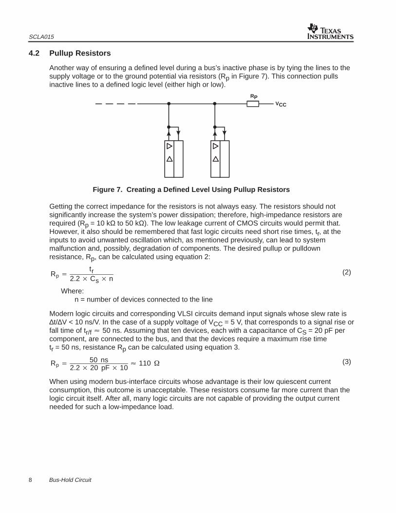
A considerably more elegant solution is to ensure a defined level for inactive bus lines viabus-hold circuits (see Figure 8). These circuits feed back the output signal of a noninvertingbuffer circuit to the input via the resistor Rf. This creates a bistable circuit (latch). To understandthe circuit, one first assumes that an active bus driver has switched the line to high level. Thismeans that a high level also exists at the output of the bus-hold circuit buffer. Thus, no currentflows via the feedback resistor Rf. The leakage currents of the circuit, which are in themicroampere region, determine power consumption of the bus-hold circuit. If the output of thebus driver in question changes to the inactive state, the bus-hold circuit holds the high level viathe feedback resistor Rf, so that now, apart from leakage currents, no current flows. Only duringthe transition of the line from high to low, or vice versa, time current spikes, which areunavoidable in CMOS circuits, occur in the bus-hold circuits. However, the dynamic powerdissipation involved is several orders of magnitude less than when using pullup resistorsdescribed previously.
Rf
1
Figure 8. Bus With Bus-Hold Circuit
This kind of circuit can be built simply by using a noninverting buffer circuit, such as theSN74AHCT541, if, as noted previously, the outputs are fed back to the inputs via resistors Rf.The propagation delay time of these components is, in this case, of secondary importance.Whether the CMOS-compatible version (SN74AHC541) or the TTL-compatible version(SN74AHCT541) is used depends on the switching thresholds of the bus-interface device. Theimpedance of the feedback resistor Rf is decided, taking into account the fact that the voltagedrop Vr at the resistor still ensures a sufficient logic level, even at the maximum leakage currentIOZ to be expected from the connected devices. Here the number of bus drivers (n) connected tothe bus obviously plays a part. In making the calculation it is assumed that, due to its low load,the output voltage of the buffer circuit used in the bus-hold circuit corresponds to the potential ofthe supply lines (VCC or GND). Thus,
RfVr
IOZ n
If we assume that ten bus drivers are connected to the bus line and that the output leakagecurrent of the bus drivers is IOZ = 10 µA, and, if we allow a voltage drop of Vr = 1 V at thefeedback resistor Rf, the resistance Rf is:
Rf1 V
10 A 10 10 k
(4)
(5)
SCLA015
10 Bus-Hold Circuit
Because with this circuit technique no charging of line capacitance is required, rather only themost recent logic level is held, problems relating to signal rise times no longer are expected.Accordingly, the circuit can be designed with considerably higher impedance, andcorrespondingly lower power consumption, than with the technology described in paragraph 4.2.
5 Integrated Bus-Hold Circuit
For the reasons given in the previous section, a defined logic level must be ensured on bus linesin the high-impedance state. Thus, it makes sense to integrate bus-hold circuits in the inputs ofbus-interface devices. Doing so means designers no longer have to concern themselves withthe problem, and additional components are not needed to ensure defined logic levels under alloperating conditions, markedly improving the reliability of the whole system.
Inputs of all newly developed bus-interface devices have a bus-hold circuit. The additional letterH in the type designation indicates this feature. An ABT device has no bus-hold circuit, while anABTH device has the additional bus-hold function. The same applies to LVT and LVC circuitsversus ALVTH, LVTH, LVCH, and ALVCH circuits.
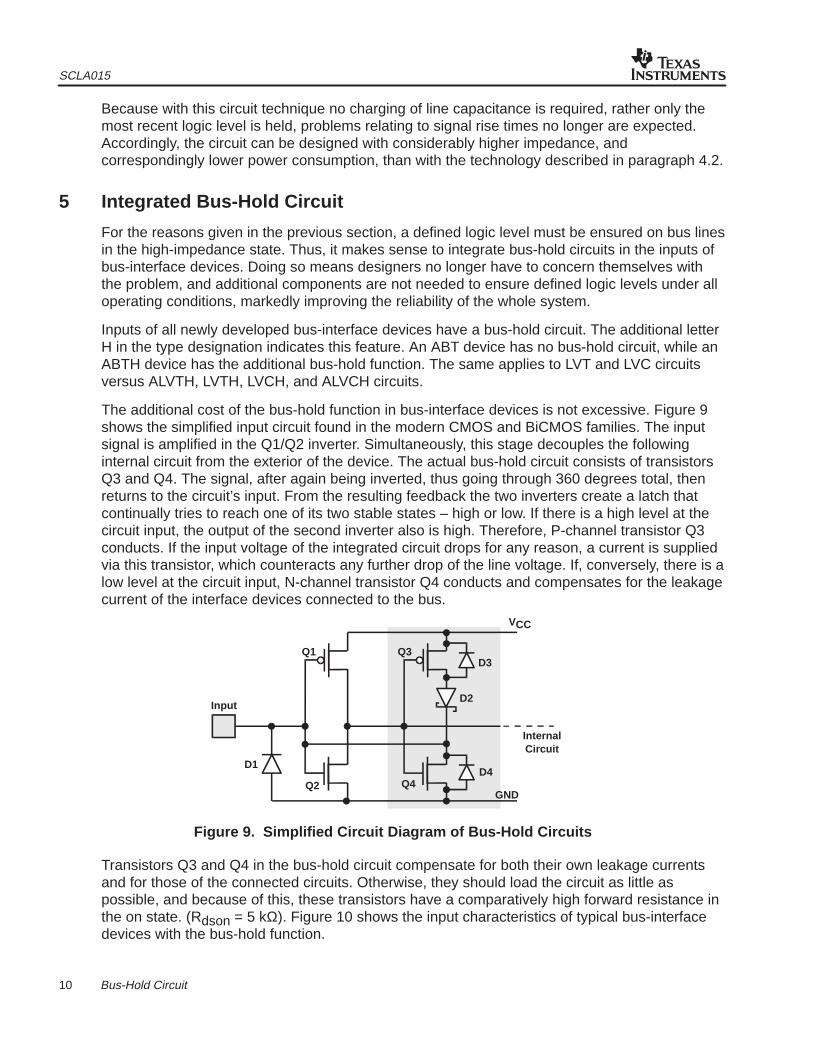
The additional cost of the bus-hold function in bus-interface devices is not excessive. Figure 9shows the simplified input circuit found in the modern CMOS and BiCMOS families. The inputsignal is amplified in the Q1/Q2 inverter. Simultaneously, this stage decouples the followinginternal circuit from the exterior of the device. The actual bus-hold circuit consists of transistorsQ3 and Q4. The signal, after again being inverted, thus going through 360 degrees total, thenreturns to the circuit’s input. From the resulting feedback the two inverters create a latch thatcontinually tries to reach one of its two stable states – high or low. If there is a high level at thecircuit input, the output of the second inverter also is high. Therefore, P-channel transistor Q3conducts. If the input voltage of the integrated circuit drops for any reason, a current is suppliedvia this transistor, which counteracts any further drop of the line voltage. If, conversely, there is alow level at the circuit input, N-channel transistor Q4 conducts and compensates for the leakagecurrent of the interface devices connected to the bus.
Q1 Q3
Q2 Q4
D1
D2
D3
D4
GND
InternalCircuit
Input
VCC
Figure 9. Simplified Circuit Diagram of Bus-Hold Circuits
Transistors Q3 and Q4 in the bus-hold circuit compensate for both their own leakage currentsand for those of the connected circuits. Otherwise, they should load the circuit as little aspossible, and because of this, these transistors have a comparatively high forward resistance inthe on state. (Rdson = 5 kΩ). Figure 10 shows the input characteristics of typical bus-interfacedevices with the bus-hold function.

SCLA015
11 Bus-Hold Circuit
V
LVTH244
ABTH245
LVCH244
II – mA
ABTH: V CC = 5 VLVTH: VCC = 3.3 VLVCH: VCC = 3.3 V
6
5
4
3
2
1
0
–1
I–
V
–1.0 –0.8 –0.6 –0.4 –0.2 0.0 0.2 0.4 0.6 0.8 1.0
Figure 10. Characteristic Input Curve of Bus-Interface Devices With the Bus-Hold Function
The switching threshold of bus-hold circuits is about 1.5 V in the devices depicted in Figure 10,matching the switching threshold of the appropriate logic circuits. If the input voltage is belowthis level, N-channel transistor Q4 conducts (Rdsontyp = 5 kΩ). This transistor also remainsconducting, even when the input voltage falls below 0 V. If the input voltage drops below –0.7 V,clamping diode D1 conducts, which protects the circuit against destruction due to electrostaticdischarge and limits negative undershoot stemming from line reflection. Above the citedthreshold voltage, P-channel transistor Q3 conducts, pulling the line level to the high potential.Diode D2 in Figure 9 prevents the parasitic diode D3 parallel to transistor Q3 from conducting ifthe input voltage has a higher positive value than the supply voltage. This last case might occur,for example, when signals with a voltage swing of 5 V control the bus-hold circuit, which is itselfoperated by a supply voltage of VCC = 3.3 V. This also ensures that the bus-hold circuit remainsat the high-impedance state with the supply voltage off. The upper diagram shows the influenceof this diode in that the bus-hold circuit already becomes high impedance at markedly less than3.3 V. In the case of ABTH devices, whose typical high level also is about 3 V despite a supplyvoltage of 5 V, it would not make sense for the bus-hold circuit to pull the potential significantlyabove this level. Accordingly, as Figure 10 shows, additional circuit features limit the rise involtage.
SCLA015
12 Bus-Hold Circuit
6 Application Information
6.1 Additional Load Caused by Bus-Hold Circuits
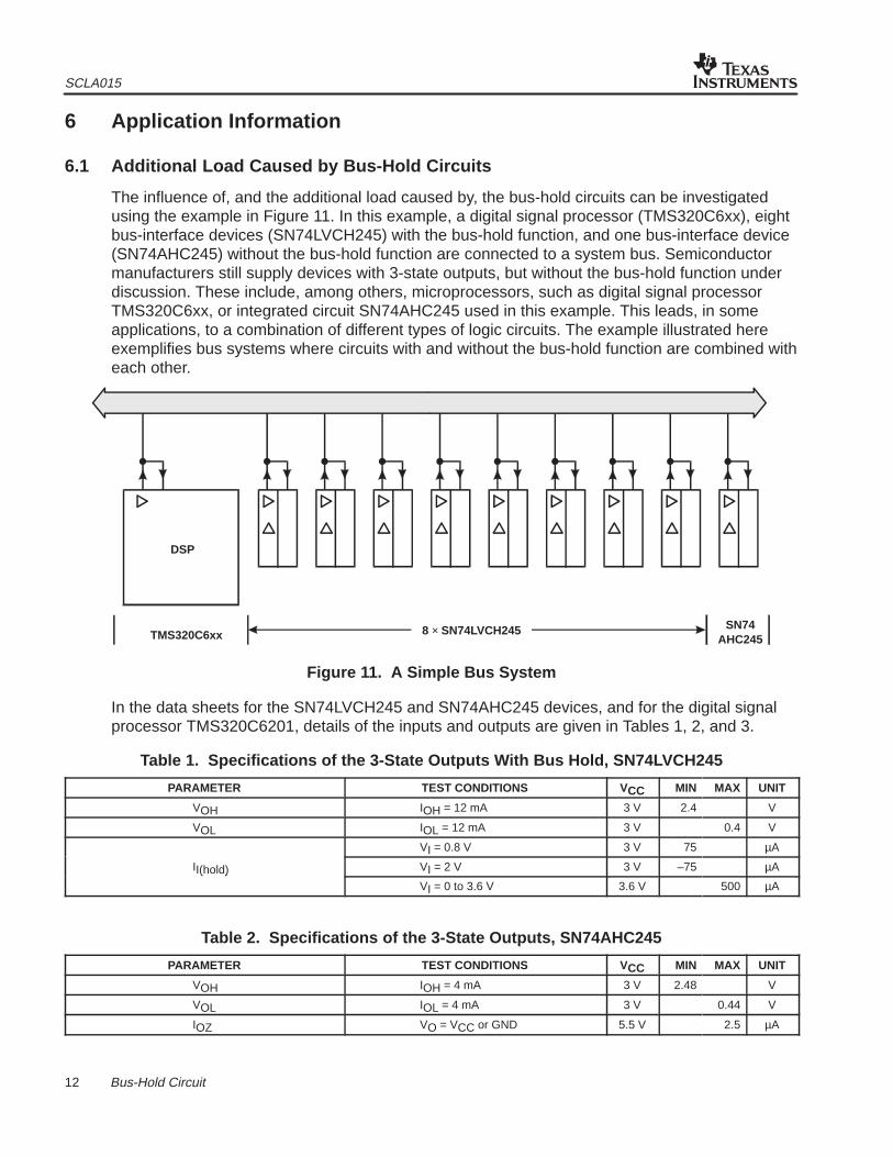
The influence of, and the additional load caused by, the bus-hold circuits can be investigatedusing the example in Figure 11. In this example, a digital signal processor (TMS320C6xx), eightbus-interface devices (SN74LVCH245) with the bus-hold function, and one bus-interface device(SN74AHC245) without the bus-hold function are connected to a system bus. Semiconductormanufacturers still supply devices with 3-state outputs, but without the bus-hold function underdiscussion. These include, among others, microprocessors, such as digital signal processorTMS320C6xx, or integrated circuit SN74AHC245 used in this example. This leads, in someapplications, to a combination of different types of logic circuits. The example illustrated hereexemplifies bus systems where circuits with and without the bus-hold function are combined witheach other.
DSP
TMS320C6xx 8 × SN74LVCH245 SN74AHC245
Figure 11. A Simple Bus System
In the data sheets for the SN74LVCH245 and SN74AHC245 devices, and for the digital signalprocessor TMS320C6201, details of the inputs and outputs are given in Tables 1, 2, and 3.
Table 1. Specifications of the 3-State Outputs With Bus Hold, SN74LVCH245ÁÁÁÁÁÁÁÁÁÁÁÁÁÁÁÁÁÁÁÁÁÁÁÁÁÁÁÁ
PARAMETERÁÁÁÁÁÁÁÁÁÁÁÁÁÁÁÁÁÁÁÁÁÁÁÁÁÁ
TEST CONDITIONSÁÁÁÁÁÁ
VCCÁÁÁÁÁÁ
MINÁÁÁÁÁÁ
MAXÁÁÁÁÁÁ
UNITÁÁÁÁÁÁÁÁÁÁÁÁÁÁÁÁÁÁÁÁÁÁÁÁÁÁÁÁ
VOHÁÁÁÁÁÁÁÁÁÁÁÁÁÁÁÁÁÁÁÁÁÁÁÁÁÁ
IOH = 12 mA ÁÁÁÁÁÁ
3 V ÁÁÁÁÁÁ
2.4ÁÁÁÁÁÁÁÁÁÁÁÁ
V
ÁÁÁÁÁÁÁÁÁÁÁÁÁÁÁÁÁÁÁÁÁÁÁÁÁÁÁÁ
VOL ÁÁÁÁÁÁÁÁÁÁÁÁÁÁÁÁÁÁÁÁÁÁÁÁÁÁ
IOL = 12 mA ÁÁÁÁÁÁ
3 V ÁÁÁÁÁÁÁÁÁÁÁÁ
0.4ÁÁÁÁÁÁ
V
ÁÁÁÁÁÁÁÁÁÁÁÁÁÁÁÁÁÁÁÁÁÁÁÁÁÁÁÁ
ÁÁÁÁÁÁÁÁÁÁÁÁÁÁÁÁÁÁÁÁÁÁÁÁÁÁ
VI = 0.8 V ÁÁÁÁÁÁ
3 V ÁÁÁÁÁÁ
75ÁÁÁÁÁÁÁÁÁÁÁÁ
µA
ÁÁÁÁÁÁÁÁÁÁÁÁÁÁÁÁÁÁÁÁÁÁÁÁÁÁÁÁ
II(hold) ÁÁÁÁÁÁÁÁÁÁÁÁÁÁÁÁÁÁÁÁÁÁÁÁÁÁ
VI = 2 V ÁÁÁÁÁÁ
3 V ÁÁÁÁÁÁ
–75ÁÁÁÁÁÁÁÁÁÁÁÁ
µA
ÁÁÁÁÁÁÁÁÁÁÁÁÁÁ( )
ÁÁÁÁÁÁÁÁÁÁÁÁÁVI = 0 to 3.6 V ÁÁÁ3.6 VÁÁÁÁÁÁ500ÁÁÁµA
Table 2. Specifications of the 3-State Outputs, SN74AHC245ÁÁÁÁÁÁÁÁÁÁÁÁÁÁÁÁÁÁÁÁÁÁÁÁÁÁÁÁ
PARAMETER ÁÁÁÁÁÁÁÁÁÁÁÁÁÁÁÁÁÁÁÁÁÁÁÁÁÁ
TEST CONDITIONS ÁÁÁÁÁÁ
VCCÁÁÁÁÁÁ
MINÁÁÁÁÁÁ
MAXÁÁÁÁÁÁ
UNIT
ÁÁÁÁÁÁÁÁÁÁÁÁÁÁÁÁÁÁÁÁÁÁÁÁÁÁÁÁ
VOH ÁÁÁÁÁÁÁÁÁÁÁÁÁÁÁÁÁÁÁÁÁÁÁÁÁÁ
IOH = 4 mA ÁÁÁÁÁÁ
3 V ÁÁÁÁÁÁ
2.48ÁÁÁÁÁÁÁÁÁÁÁÁ
V
ÁÁÁÁÁÁÁÁÁÁÁÁÁÁÁÁÁÁÁÁÁÁÁÁÁÁÁÁ
VOL ÁÁÁÁÁÁÁÁÁÁÁÁÁÁÁÁÁÁÁÁÁÁÁÁÁÁ
IOL = 4 mA ÁÁÁÁÁÁ
3 V ÁÁÁÁÁÁÁÁÁÁÁÁ
0.44ÁÁÁÁÁÁ
V
ÁÁÁÁÁÁÁÁÁÁÁÁÁÁÁÁÁÁÁÁÁÁÁÁÁÁÁÁ
IOZ ÁÁÁÁÁÁÁÁÁÁÁÁÁÁÁÁÁÁÁÁÁÁÁÁÁÁ
VO = VCC or GND ÁÁÁÁÁÁ
5.5 VÁÁÁÁÁÁÁÁÁÁÁÁ
2.5ÁÁÁÁÁÁ
µA
SCLA015
13 Bus-Hold Circuit
Table 3. Specifications of the 3-State Outputs, TMS320C6201
ÁÁÁÁÁÁÁÁÁÁÁÁÁÁÁÁÁÁÁÁÁÁÁÁÁÁ
PARAMETER ÁÁÁÁÁÁÁÁÁÁÁÁÁÁÁÁÁÁÁÁÁÁÁÁÁÁ
TEST CONDITIONS ÁÁÁÁÁÁ
VCCÁÁÁÁÁÁ
MINÁÁÁÁÁÁ
MAXÁÁÁÁÁÁ
UNIT
ÁÁÁÁÁÁÁÁÁÁÁÁÁVOH ÁÁÁÁÁÁÁÁÁÁÁÁÁIOH = 12 mA ÁÁÁ3.14 VÁÁÁ2.4ÁÁÁÁÁÁVÁÁÁÁÁÁÁÁÁÁÁÁÁÁÁÁÁÁÁÁÁÁÁÁÁÁVOL
ÁÁÁÁÁÁÁÁÁÁÁÁÁÁÁÁÁÁÁÁÁÁÁÁÁÁIOL = 12 mA
ÁÁÁÁÁÁ3.14 VÁÁÁÁÁÁÁÁÁÁÁÁ0.4ÁÁÁÁÁÁVÁÁÁÁÁÁÁÁÁÁÁÁÁ
ÁÁÁÁÁÁÁÁÁÁÁÁÁIOZ
ÁÁÁÁÁÁÁÁÁÁÁÁÁÁÁÁÁÁÁÁÁÁÁÁÁÁ
VO = 0 V or DVDDÁÁÁÁÁÁ
3.46 VÁÁÁÁÁÁÁÁÁÁÁÁ
10ÁÁÁÁÁÁ
µA
With respect to sufficient logic levels (VIL < 0.8 V, VIH > 2.0 V), the bus-hold circuit in theSN74LVCH245 device supplies a current of II(hold) > |75 µA|. Assuming a maximum leakagecurrent of IOZmax = 10 µA for 3-state outputs, a single bus-hold device would almost be capableon its own to compensate the leakage currents of the other nine devices connected to the busand ensure defined levels on the bus lines. This is all the more so that, in practice, as notedabove, none of the integrated circuits show the maximum output leakage currents IOZ given inthe data sheets. Due to the large variation of the transistor parameters caused by productionvariations and changes in supply voltage and temperature, the maximum current II(hold) mightrise to 500 µA (see Figure 10). In the example shown here, a single active output also must beable to charge/discharge the device’s capacitance and to switch eight inputs with bus hold. Theoutputs of the LVCH and AHC devices, and the processor, can supply a current of8 × II(hold)max = 4 mA (see Tables 1, 2, and 3).
6.2 Influence on the Circuit’s Power Loss
When using bus-hold circuits, a current, II(hold), flows during signal state transition from low tohigh and from high to low for the duration of the signal slope, which has an influence on thesystem’s power consumption. The resultant power dissipation can be calculated approximately.
According to Table 1, the maximum current in bus-interface device SN74LVCH245 isII(hold)max = 500 µA at VCCmax = 3.6 V. Because the current during a signal transition follows aroughly triangular shape, we can derive the power consumption, Phold, caused during signaltransitions by the bus-hold circuits:
Phold12 VCC II(hold)max tr 2 f n
Where:tr = signal rise or fall timef = frequency of signal exchangen = number of inputs with a bus-hold circuitII(hold)max = maximum bus-hold circuit input current
For the SN74LVCH245 device, n = 8. If we assume that the mean frequency, f, of signaltransitions at the inputs = 10 MHz, the rise time, tr = 2 ns, yielding:
Phold12 3.6 V 500 A 2 ns 2 10 MHz 8 0.288 mW
Equation 7 predicts that the parameter Phold increases with longer rise times. In contrast, thereis the dynamic power dissipation, Pdyn, of the circuit, which, taking the power dissipationcapacitance Cpd = 31 pF given in the device’s data sheet, can be calculated:
Pdyn Cpd VCC2 f n
31 pF 3.62 10 MHz 8 320 mW
(6)
(7)
(8)
SCLA015
14 Bus-Hold Circuit
Because power consumption Phold caused by the bus-hold circuit is several orders of magnitudeless than this, it safely can be disregarded.
6.3 Presetting Logic Levels
Some applications require specific logic levels on certain bus lines during the initialization phaseafter the supply voltage is switched on. The microprocessor queries this level and makes certainsystem settings (start vector, etc.) on the basis of the information it reads. In conventionalbus-interface devices, the desired level is generated on the lines in question via pullup orpulldown resistors. Because the input resistances of CMOS circuits are very high,high-impedance resistors (10 kΩ to100 kΩ) do this job very well.
When using interface devices with the bus-hold function, however, additional attention has to bepaid to this circuit detail. Hold circuits have an inherent tendency to generate a low level whenthe supply voltage is switched on. As noted previously, this circuit behaves like a latch. Acomparatively large capacitance – the interconnect lines and other circuit components – isconnected to its set input (the input of the integrated circuit). This capacitance is dischargedwhen the supply voltage is switched on. This is the reason that a low level is generated therewhen the voltage is switched on. Because the bus-hold circuit still has a very high impedanceduring the first moment of the power-on phase (VCC ≤ Vt), a high-impedance pullup resistor(10 kΩ to 100 kΩ), at this point in time, would be able to put the latch into the opposite logicstate and generate a high level at the input of the bus-hold circuit. However, this observationdoes not take into account the fact that other devices connected to this bus might couple chargeinto the previously mentioned capacitance during supply-voltage startup, thus forcing a differentlevel from the one expected. In this respect, the outputs of the interface devices connected tothe bus are more effective than the bus-hold circuit and an associated preset circuit. If theoutputs during the power-on phase briefly enter an undesired active state, they force thebus-hold circuit to the output’s state. Then, a high-impedance pullup or pulldown resistor is nolonger able to change this state.
Consequently, the only way to force the device to a certain state is to place suitablelow-impedance pullup or pulldown resistors. According to the maximum input current to abus-hold circuit, II(hold)max = 500 µA. This current flows when a hold-circuit threshold voltage ofVt = 1.5 V is reached (see Figure 10). Taking this figure, the value for pullup resistance, Rp, canbe calculated:
RpVCCmin Vt
II(hold)max
If an LVCH circuit is connected to the bus, the resistance is calculated as:
Rp3.0 V 1.5 V
500 A 3 k
If several devices with the bus-hold function are connected to the bus, the resistance value mustbe reduced accordingly.
(9)
(10)

SCLA015
15 Bus-Hold Circuit
7 Summary
This application report addresses the question of how to ensure defined levels on bus lineswhen all bus drivers are in the inactive high-impedance state (3-state). This is of particularimportance in the case of smaller CMOS-based systems where, for technical reasons, the linescannot be terminated by a resistor network matched to the line impedance. This applicationreport presents various different circuit options, with particular reference to a novel bus-holdcircuit that TI integrates into modern bus-interface devices. This additional circuit provides anideal combination of all the functions needed for a bus system to run properly. These include:
• Ensuring a defined logic level when the bus is in the inactive state (3-state).
• Avoiding excessive supply current due to logic levels that lie outside the limits stipulated indata sheets. To this end, a bus-hold circuit often is a must for battery-operated systems.
• The bus-hold circuit also prevents oscillation of the bus-interface devices provoked byundefined logic levels. Combined with appropriate power consumption, this measurepromotes both the reliability and the electromagnetic compatibility of the system.

IMPORTANT NOTICE
Texas Instruments and its subsidiaries (TI) reserve the right to make changes to their products or to discontinueany product or service without notice, and advise customers to obtain the latest version of relevant informationto verify, before placing orders, that information being relied on is current and complete. All products are soldsubject to the terms and conditions of sale supplied at the time of order acknowledgment, including thosepertaining to warranty, patent infringement, and limitation of liability.
TI warrants performance of its products to the specifications applicable at the time of sale in accordance withTI’s standard warranty. Testing and other quality control techniques are utilized to the extent TI deems necessaryto support this warranty. Specific testing of all parameters of each device is not necessarily performed, exceptthose mandated by government requirements.
Customers are responsible for their applications using TI components.
In order to minimize risks associated with the customer’s applications, adequate design and operatingsafeguards must be provided by the customer to minimize inherent or procedural hazards.
TI assumes no liability for applications assistance or customer product design. TI does not warrant or representthat any license, either express or implied, is granted under any patent right, copyright, mask work right, or otherintellectual property right of TI covering or relating to any combination, machine, or process in which suchproducts or services might be or are used. TI’s publication of information regarding any third party’s productsor services does not constitute TI’s approval, license, warranty or endorsement thereof.
Reproduction of information in TI data books or data sheets is permissible only if reproduction is withoutalteration and is accompanied by all associated warranties, conditions, limitations and notices. Representationor reproduction of this information with alteration voids all warranties provided for an associated TI product orservice, is an unfair and deceptive business practice, and TI is not responsible nor liable for any such use.
Resale of TI’s products or services with statements different from or beyond the parameters stated by TI forthat product or service voids all express and any implied warranties for the associated TI product or service,is an unfair and deceptive business practice, and TI is not responsible nor liable for any such use.
Also see: Standard Terms and Conditions of Sale for Semiconductor Products. www.ti.com/sc/docs/stdterms.htm
Mailing Address:
Texas InstrumentsPost Office Box 655303Dallas, Texas 75265
Copyright 2001, Texas Instruments Incorporated