Embed Size (px)
Citation preview

c© 2016 Ankit Jain
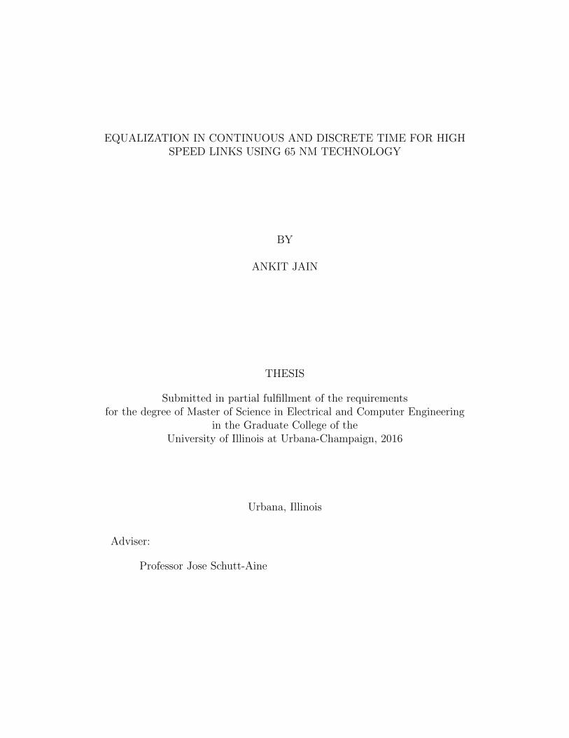
EQUALIZATION IN CONTINUOUS AND DISCRETE TIME FOR HIGHSPEED LINKS USING 65 NM TECHNOLOGY
BY
ANKIT JAIN
THESIS
Submitted in partial fulfillment of the requirementsfor the degree of Master of Science in Electrical and Computer Engineering
in the Graduate College of theUniversity of Illinois at Urbana-Champaign, 2016
Urbana, Illinois
Adviser:
Professor Jose Schutt-Aine
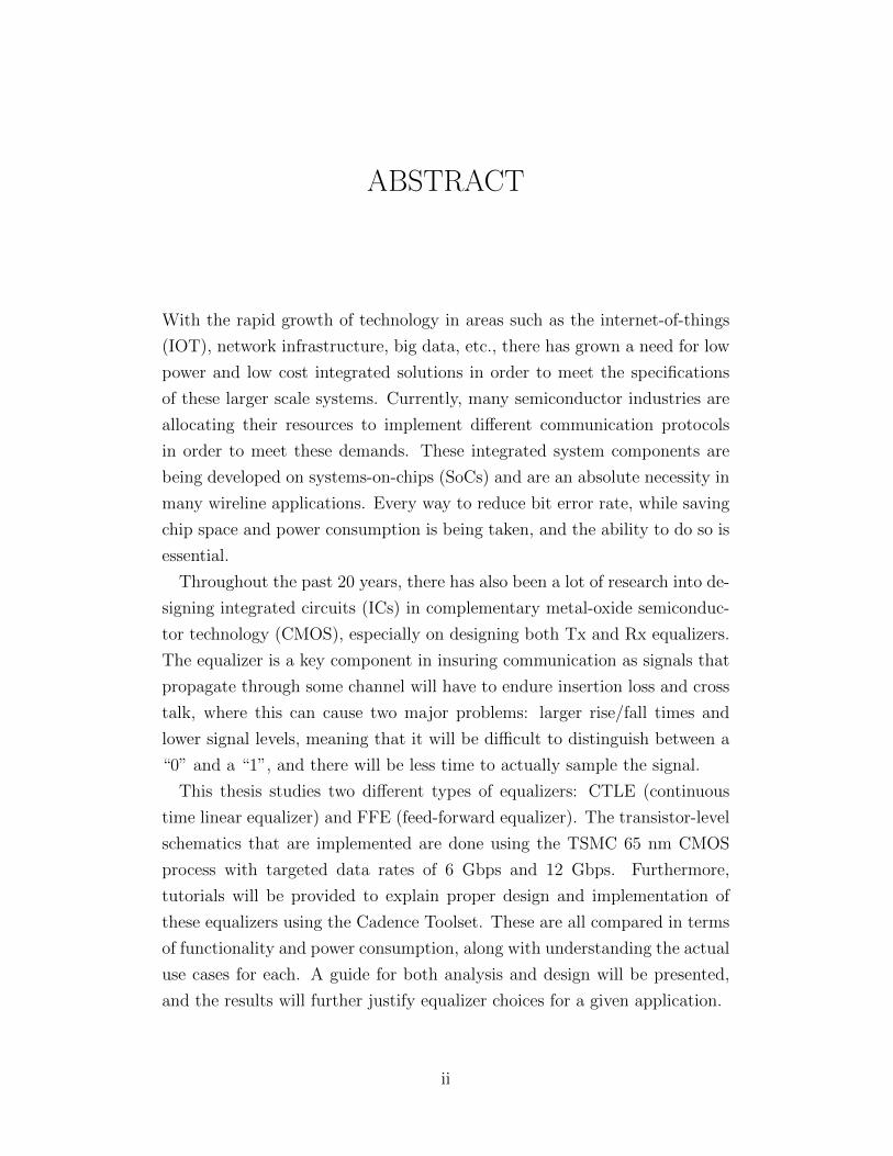
ABSTRACT
With the rapid growth of technology in areas such as the internet-of-things
(IOT), network infrastructure, big data, etc., there has grown a need for low
power and low cost integrated solutions in order to meet the specifications
of these larger scale systems. Currently, many semiconductor industries are
allocating their resources to implement different communication protocols
in order to meet these demands. These integrated system components are
being developed on systems-on-chips (SoCs) and are an absolute necessity in
many wireline applications. Every way to reduce bit error rate, while saving
chip space and power consumption is being taken, and the ability to do so is
essential.
Throughout the past 20 years, there has also been a lot of research into de-
signing integrated circuits (ICs) in complementary metal-oxide semiconduc-
tor technology (CMOS), especially on designing both Tx and Rx equalizers.
The equalizer is a key component in insuring communication as signals that
propagate through some channel will have to endure insertion loss and cross
talk, where this can cause two major problems: larger rise/fall times and
lower signal levels, meaning that it will be difficult to distinguish between a
“0” and a “1”, and there will be less time to actually sample the signal.
This thesis studies two different types of equalizers: CTLE (continuous
time linear equalizer) and FFE (feed-forward equalizer). The transistor-level
schematics that are implemented are done using the TSMC 65 nm CMOS
process with targeted data rates of 6 Gbps and 12 Gbps. Furthermore,
tutorials will be provided to explain proper design and implementation of
these equalizers using the Cadence Toolset. These are all compared in terms
of functionality and power consumption, along with understanding the actual
use cases for each. A guide for both analysis and design will be presented,
and the results will further justify equalizer choices for a given application.
ii

To my parents, for their love and support throughout all of my education
and experiences.
iii

ACKNOWLEDGMENTS
As I step closer and closer towards earning my master’s degree, I now realize
the amount of work I have accomplished and all of the people who have
pushed me to do so. While taking initiative in this research and writing this
thesis, I also am proud to have the support, effort, and motivation of different
people throughout my experience.
I want to start by thanking my adviser, Professor Jose Schutt-Aine, for be-
ing a constant source of knowledge, encouragement, and motivation through-
out my graduate experience, along with my later years as an undergraduate
student. No matter what, he always put in the effort to make sure that I
did not have any trouble in finding the resources I needed to accomplish my
work. When I originally joined his research group, it was clear what area my
research would focus on, but he gave me full control over the content itself.
I would visit his office frequently to ask for advice and provide updates on
my progress, which would always be met by his constant enthusiasm and
encouragement. As a professional, I look forward to showing him how all
of his efforts as an adviser paid off, and I will always look up to him as I
continue in my career.
Secondly, I want to thank many faculty in the ECE Department who have
been continuous sources of inspiration, knowledge, research, and so much
more. Professor Carney provided me with the opportunity to take on re-
search within optics, while also driving me to be one of his lead Teaching
Assistants in the Senior Design course. He would provide me with humor,
life advice, and a positive attitude that would keep reminding me why I made
the decision to be an engineer in the first place. Professor Makela, like Pro-
fessor Carney, was another one of the major influences in my role as a Senior
Design Teaching Assistant. He has led me as a research mentor, a professor,
and now as a course instructor, and I’m very proud to show my maturity
as an engineer as I take on my next role. Professor Oelze, Professor Singer,
iv

Professor Kumar, Professor Swenson, and Dr. Galvin have all continued
what Professor Carney and Professor Makela initiated as mentors within the
Senior Design Course. Thanks to all of them, I have grown as an engineer,
as a professional, and as a person. Professor Sanders, Professor Franke, and
Professor Kudeki have been amazing sources of motivation and encourage-
ment with my abilities as a leader. Thanks to their patience and enthusiasm
with my constant visits to their offices, I feel that I have helped in improving
this department, while building strong professional relationships that I look
forward to maintaining for the years to come. Professor Bernhard started
as my appointed faculty mentor when I was an undergraduate student, and
continued as an excellent source of advice and technical discussion through-
out my graduate experience. Professor Hanumolu helped me find my initial
inspiration in integrated circuits and turn it into something greater. With
his teaching and advice in IC Design, I feel proud to have accomplished the
work shown in this thesis.
Next, I want to thank the graduate and undergraduate students within
Professor Schutt-Aine’s research group for their effort, constructive criticism,
and encouragement. I want to start by thanking Da Wei, who has been an
amazing source of knowledge and encouragement as I started in this group,
and has provided me with many resources, papers, and books to read from in
order to understand the different aspects of equalization. Alongside that, he
has done an amazing job of maintaining the servers and tools for our group
to continue its research. I would like to thank Rushabh Mehta, Zexian Li, Yi
Ren, and Ishita Bisht for their contributions towards the SERDES project
that we have all undergone together. I would also like to thank Xu Chen for
his constructive criticism, constant visits, and discussions regarding different
aspects of engineering. Lastly, while these members have already graduated
and started their next chapters, I would like to thank Sabareesh Kumar,
Drew Handler, Drew Newell, Yubo Liu, Lei Jin, and Thomas Comberiate for
providing me with an amazing transition into this group in Fall 2013, and
for leaving behind an amazing legacy for future students to follow.
As I think outside of my research, I think of the great friends who have
given great research, professional, and technical advice while cheering me on
throughout all of my challenges during my graduate experience. With this,
I want to thank Cara Yang, Benjamin Cahill, Jacob Bryan, Liana Nicklaus,
Li Ma, Matthew Tischer, David Walder, Tej Chajed, Nikita Parikh, Achal
v

Varma, Vignesh Vishwanathan, Koushik Roy, Denise Li, Aswin Sivaraman,
Anthony Vesuvio, Shaila Altschuler, Radha Patel, Jacqui Milara, and Monica
Rito. Unfortunately, there are many more people I have not included, but I
still thank you all for your consistent support and encouragement.
Finally, I want to thank my family. I’m glad to follow in the footsteps
of my parents by pursuing engineering, and I’m proud to have many results
to show for it. My uncle and aunt, who also studied electrical engineering
through graduate school, have given me great advice and encouragement as I
pursued my graduate degree. My family have been amazing (and patient) as
I’ve grown, and have stayed by my side throughout all the challenging steps.
Thanks to them, I am excited and proud to step into the next chapter of my
life.
vi
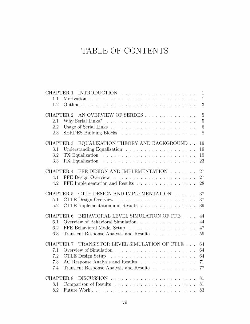
TABLE OF CONTENTS
CHAPTER 1 INTRODUCTION . . . . . . . . . . . . . . . . . . . . 11.1 Motivation . . . . . . . . . . . . . . . . . . . . . . . . . . . . . 11.2 Outline . . . . . . . . . . . . . . . . . . . . . . . . . . . . . . . 3
CHAPTER 2 AN OVERVIEW OF SERDES . . . . . . . . . . . . . . 52.1 Why Serial Links? . . . . . . . . . . . . . . . . . . . . . . . . 52.2 Usage of Serial Links . . . . . . . . . . . . . . . . . . . . . . . 62.3 SERDES Building Blocks . . . . . . . . . . . . . . . . . . . . 8
CHAPTER 3 EQUALIZATION THEORY AND BACKGROUND . . 193.1 Understanding Equalization . . . . . . . . . . . . . . . . . . . 193.2 TX Equalization . . . . . . . . . . . . . . . . . . . . . . . . . 193.3 RX Equalization . . . . . . . . . . . . . . . . . . . . . . . . . 23
CHAPTER 4 FFE DESIGN AND IMPLEMENTATION . . . . . . . 274.1 FFE Design Overview . . . . . . . . . . . . . . . . . . . . . . 274.2 FFE Implementation and Results . . . . . . . . . . . . . . . . 28
CHAPTER 5 CTLE DESIGN AND IMPLEMENTATION . . . . . . 375.1 CTLE Design Overview . . . . . . . . . . . . . . . . . . . . . 375.2 CTLE Implementation and Results . . . . . . . . . . . . . . . 39
CHAPTER 6 BEHAVIORAL LEVEL SIMULATION OF FFE . . . . 446.1 Overview of Behavioral Simulation . . . . . . . . . . . . . . . 446.2 FFE Behavioral Model Setup . . . . . . . . . . . . . . . . . . 476.3 Transient Response Analysis and Results . . . . . . . . . . . . 59
CHAPTER 7 TRANSISTOR LEVEL SIMULATION OF CTLE . . . 647.1 Overview of Simulation . . . . . . . . . . . . . . . . . . . . . . 647.2 CTLE Design Setup . . . . . . . . . . . . . . . . . . . . . . . 647.3 AC Response Analysis and Results . . . . . . . . . . . . . . . 717.4 Transient Response Analysis and Results . . . . . . . . . . . . 77
CHAPTER 8 DISCUSSION . . . . . . . . . . . . . . . . . . . . . . . 818.1 Comparison of Results . . . . . . . . . . . . . . . . . . . . . . 818.2 Future Work . . . . . . . . . . . . . . . . . . . . . . . . . . . . 83
vii

REFERENCES . . . . . . . . . . . . . . . . . . . . . . . . . . . . . . . 87
viii
CHAPTER 1
INTRODUCTION
1.1 Motivation
Some of the biggest accomplishments over these past few decades have been
the advancements made within the area of computing and data processing.
This has spawned many new realms recently, such as Big Data, the Internet
of Things (IOT), and much more [1]. The increasing demand for faster data
rates has driven the desire for research and implementation of new circuits,
systems, and communication protocols. Integrated circuit (IC) technology
has been continuously reducing in size while increasing in its processing abil-
ity. We are able to reach frequencies and data rates that are in several tens
to hundreds of GHz and Gbps, where less than two decades ago, that was the
ideal goal of many different research labs. As we go smaller and faster, we
realize that we are seeing the limits within IC design, as there is a significant
trade-off between size, speed, and power consumption.
These limitations have driven the need for dedicated Systems-on-Chips
(SOCs) that are essential to ensure efficient communication, especially with
interfaces like processor-to-memory on computers and fiber-optic internet.
One thing that needs to be taken into account is how scaling the links relates
to scaling the data rates. Since both scalings are not properly proportional,
this results in a massive bottleneck in high speed link design and performance.
Another set of issues comes with the loss characteristics of the channel
themselves (backplanes, traces, etc.). Large amounts of insertion loss, cross
talk, and signal distortion from these transmission lines result in a lot of
intersymbol interference (ISI). With these further degrading characteristics,
the demand for fast and efficient equalizers has become a major factor in the
industry.
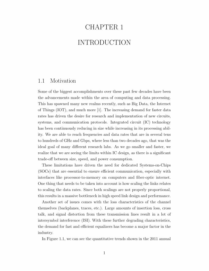
In Figure 1.1, we can see the quantitative trends shown in the 2011 annual
1
Figure 1.1: Input/Output Link Data Rate Trends [2]
semiconductor roadmapping report from the International Solid State Cir-
cuits Conference (ISSCC) [2]. On average we see a rise in 2X every 4 years
in the data rates, yet the channel bandwidth is still the same. Another thing
to notice is that the majority of research discusses the fundamentals and the
mathematics behind equalization, yet none provide a comprehensive tutorial
and understanding of the actual implementation.
There are many examples where they discuss the design of some equalizers
in detail, especially in cases including novel designs, but none go through the
understanding and implementation of the simulation itself. As these tool sets
are very broad and cover a lot of areas, it is essential to provide some guides
and understanding towards the simulation procedure within an electronic
design automation (EDA) toolset.
As the data rates increase, so do the insertion loss, cross talk, and even the
parasitics of the transmitting media. Due to this, there is an increasing need
for equalizers, and in designing these, circuit designers need to understand
not only the amount of loss to recover, but also the delays to reduce, the
jitter characteristics, and lastly, the specifications and performance issues
of other blocks in the system, especially with the clock and data recovery
(CDR) circuit.
With all of this, the motivation of this thesis is simply this: To fill the gap
2
that exists between the fundamental and theoretical aspects of the equalizer
design and the simulation and execution stages that signal integrity engineers
will have to go through, by providing a basic expertise in both realms and in
the effective design of high speed systems.
1.2 Outline
This thesis aims to accomplish two major goals: The first is to provide
an elaborate understanding of equalization and the design process behind a
continuous-time and a discrete-time based equalizer. The second is to provide
a comprehensive tutorial for students entering/planning to enter graduate
school to study mixed-signal integrated circuit design. By going through the
theory, the design process, and the simulation process, users of this tutorial
will get a well-rounded understanding of the implementation and simulation
of high speed links, with a key emphasis on equalization.
1. Chapter 1 provides the motivation behind the research problem, along
with some justification for the key emphasis on equalization.
2. Chapter 2 gives an overview on high speed serial links (HSSLs) by
going through each of the blocks that goes into building an end-to-end
serializer-deserializer (SerDes) system, along with further justifying the
need and benefits of serial links over parallel links.
3. Chapter 3 discusses the theory that justifies the need for equalization,
along with some basic understanding of equalization techniques on its
own (outside of the SerDes system).
4. Chapter 4 introduces the feed-forward equalizer (FFE) and provides
an explanation of both the design process and an implementation with
results.
5. Chapter 5 introduces the continuous time linear equalizer (CTLE) and,
similar to Chapter 4, provides an explanation of both the design process
towards building one, along with an implementation with results.
3
6. Chapter 6 explains the procedure for setting up the behavioral model
of an FFE. Afterwards, the procedure describes the testbench setup for
simulating a transient response.
7. Chapter 7 explains the procedure for building, simulation, and analyz-
ing a transistor-level CTLE in both the time and frequency domains.
8. Chapter 8 concludes the thesis by explaining the overall accomplish-
ments from the different implementations of the equalizers, and then
discusses the future utilizations of these techniques towards more com-
plex designs with an understanding of the design process behind it.
4
CHAPTER 2
AN OVERVIEW OF SERDES
2.1 Why Serial Links?
The first thing to understand, before we delve into serial links, is the transi-
tion from parallel links to serial links in many applications. Most input/out
(I/O) systems that connect to processing units do so via communication
interfaces like peripheral component interconnects (PCI/PCI-X) and inte-
grated drive electronics (IDE). Due to the parallel nature of these links, wide
data buses were required in order to handle sending each bit of the trans-
mitted data, as they each required their own conductors. Due to this im-
plementation, data rates were limited to speeds less than hundreds of Mb/s
[3]. Anything with higher performance was typically used in larger scale
supercomputers and work stations.
Over the past 20 years, data rates have started increasing. The fix to these
parallel links was to increase the number of conductors [4], but again, we see
an issue of cost and space becoming a major problem in this “solution.” By
transitioning to serial links, we are able to avoid those two major bottle-
necks. From this transition, interfaces like PCI-Express (PCIe) and Serial
ATA (SATA) were developed and are still used in computers today.
Serial Links are able to address some of the really important factors in
design specifications: cost, space, bandwidth, and power. By utilizing a
serial link topology over a parallel link, there is an immediate drop in cost
and used space. Finally, without using parallel links, there is no longer
a usage of really wide data buses, resulting in larger bandwidths for data
transfer.
Furthermore, serial links mitigate issues in crosstalk because the high speed
parallel signals do not electromagnetically interfere with each other. Since
all of the data is being transferred on one line, you eliminate the problem
5
of data skew, while still having more burden on a single line. In the case of
parallel links, the parasitics of the conductors can cause potential differences
in the delays towards the received signals. Lastly, as the transistor sizes scale
down, the supply voltages for serial links will also scale down significantly,
which unfortunately is not the case for parallel link buses [5].
In the case of area, utilizing serial links means a decrease in the amount of
traces used on the motherboard’s printed circuit board (PCB). This provides
more flexibility in the packaging for processor’s IC, along with improving
isolation. Along with saving traces on data, serial links will also eliminate
the clock trace, as it is not necessary to send transmitter (TX) clock with
the data itself.
With all of these significant improvements that are introduced by the uti-
lization of serial links over parallel links, serial links have proven themselves
to be the solution towards reaching our goals of increased data rates and
higher transmission efficiency that the industry truly needs.
2.2 Usage of Serial Links
Serial links have many different uses in today’s society, such as telecom
companies that utilize fiber optics and computers with local access net-
work (LAN) cables. Also, a very common usage is with backplane PCB
traces. Backplanes are very popularly used in data centers, work stations,
etc. Through utilization of line cards, data can be transmitted through the
backplane via high speed SERDES chips.
Line cards are utilized as follows: ICs are mounted onto packages to be
soldered onto the line card. Then, the line cards are connected via through
hole connectors and use the backplane channel as their transmitting medium.
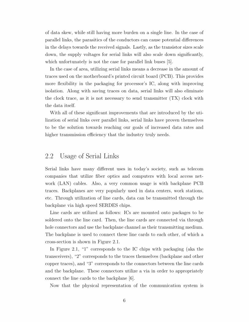
The backplane is used to connect these line cards to each other, of which a
cross-section is shown in Figure 2.1.
In Figure 2.1, “1” corresponds to the IC chips with packaging (aka the
transceivers), “2” corresponds to the traces themselves (backplane and other
copper traces), and “3” corresponds to the connectors between the line cards
and the backplane. These connectors utilize a via in order to appropriately
connect the line cards to the backplane [6].
Now that the physical representation of the communication system is
6
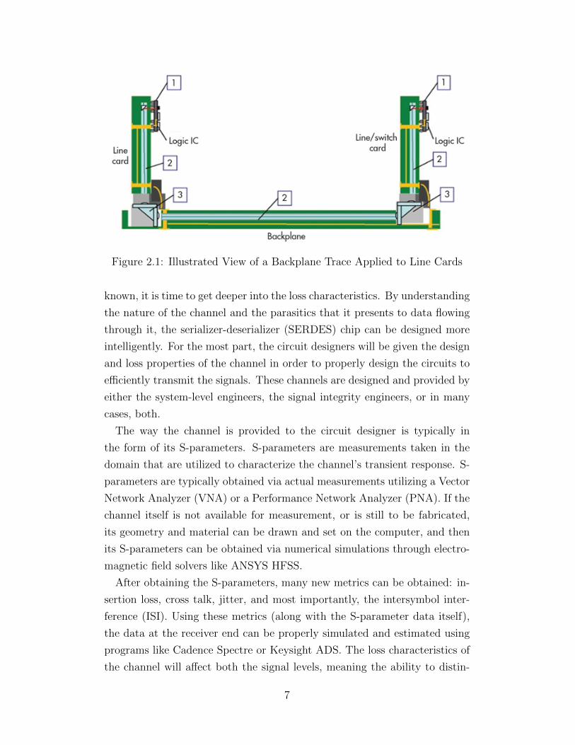
Figure 2.1: Illustrated View of a Backplane Trace Applied to Line Cards
known, it is time to get deeper into the loss characteristics. By understanding
the nature of the channel and the parasitics that it presents to data flowing
through it, the serializer-deserializer (SERDES) chip can be designed more
intelligently. For the most part, the circuit designers will be given the design
and loss properties of the channel in order to properly design the circuits to
efficiently transmit the signals. These channels are designed and provided by
either the system-level engineers, the signal integrity engineers, or in many
cases, both.
The way the channel is provided to the circuit designer is typically in
the form of its S-parameters. S-parameters are measurements taken in the
domain that are utilized to characterize the channel’s transient response. S-
parameters are typically obtained via actual measurements utilizing a Vector
Network Analyzer (VNA) or a Performance Network Analyzer (PNA). If the
channel itself is not available for measurement, or is still to be fabricated,
its geometry and material can be drawn and set on the computer, and then
its S-parameters can be obtained via numerical simulations through electro-
magnetic field solvers like ANSYS HFSS.
After obtaining the S-parameters, many new metrics can be obtained: in-
sertion loss, cross talk, jitter, and most importantly, the intersymbol inter-
ference (ISI). Using these metrics (along with the S-parameter data itself),
the data at the receiver end can be properly simulated and estimated using
programs like Cadence Spectre or Keysight ADS. The loss characteristics of
the channel will affect both the signal levels, meaning the ability to distin-
7
Figure 2.2: SERDES Implementation with Representation of LossCharacteristics [7]
guish between a “0” and a “1”, and the sampling time, meaning the window
of time that the receiver end has to properly analyze the bit. An example of
this is shown in Figure 2.2 [7].
On the transmitter end, the data (transmitted at a rate of 10 Gb/s) is sent
properly, such that it is clear enough to distinguish between a “0” and a “1”
and there is enough room to sample each bit. However, at the receiver end,
there is so much interference in the data that there is no appropriate time to
sample the bits, nor are there any clear signal levels to distinguish between
“0” and “1”. Because of this, a proper receiver needs to be designed not only
to clean up the received data stream, but also to sample the data accurately
and efficiently, with a minimal bit error rate (typically less than 10−13 [1 in
every 1013 bits]). There can also be some work done on the transmitting end
as well to reduce the degrading effects of the channel, all of which will be
explained in the following chapters.
2.3 SERDES Building Blocks
A typical implementation of a SerDes system is shown in Figure 2.3, and
each block is explained in Sections 2.3.1 - 2.3.9.
8
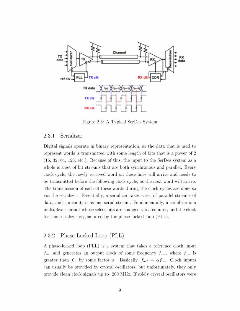
Figure 2.3: A Typical SerDes System
2.3.1 Serializer
Digital signals operate in binary representation, so the data that is used to
represent words is transmitted with some length of bits that is a power of 2
(16, 32, 64, 128, etc.). Because of this, the input to the SerDes system as a
whole is a set of bit streams that are both synchronous and parallel. Every
clock cycle, the newly received word on these lines will arrive and needs to
be transmitted before the following clock cycle, as the next word will arrive.
The transmission of each of these words during the clock cycles are done so
via the serializer. Essentially, a serializer takes a set of parallel streams of
data, and transmits it as one serial stream. Fundamentally, a serializer is a
multiplexer circuit whose select bits are changed via a counter, and the clock
for this serializer is generated by the phase-locked loop (PLL).
2.3.2 Phase Locked Loop (PLL)
A phase-locked loop (PLL) is a system that takes a reference clock input
fin, and generates an output clock of some frequency fout, where fout is
greater than fin by some factor α. Basically, fout = αfin. Clock inputs
can usually be provided by crystal oscillators, but unfortunately, they only
provide clean clock signals up to 200 MHz. If solely crystal oscillators were
9
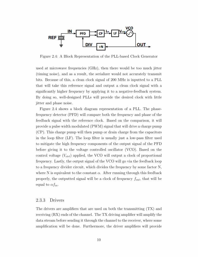
Figure 2.4: A Block Representation of the PLL-based Clock Generator
used at microwave frequencies (GHz), then there would be too much jitter
(timing noise), and as a result, the serializer would not accurately transmit
bits. Because of this, a clean clock signal of 200 MHz is inputted to a PLL
that will take this reference signal and output a clean clock signal with a
significantly higher frequency by applying it to a negative-feedback system.
By doing so, well-designed PLLs will provide the desired clock with little
jitter and phase noise.
Figure 2.4 shows a block diagram representation of a PLL. The phase-
frequency detector (PFD) will compare both the frequency and phase of the
feedback signal with the reference clock. Based on the comparison, it will
provide a pulse width modulated (PWM) signal that will drive a charge pump
(CP). This charge pump will then pump or drain charge from the capacitors
in the loop filter (LF). The loop filter is usually just a low-pass filter used
to mitigate the high frequency components of the output signal of the PFD
before giving it to the voltage controlled oscillator (VCO). Based on the
control voltage (Vctrl) applied, the VCO will output a clock of proportional
frequency. Lastly, the output signal of the VCO will go via the feedback loop
to a frequency divider circuit, which divides the frequency by some factor N,
where N is equivalent to the constant α. After running through this feedback
properly, the outputted signal will be a clock of frequency fout, that will be
equal to αfin.
2.3.3 Drivers
The drivers are amplifiers that are used on both the transmitting (TX) and
receiving (RX) ends of the channel. The TX driving amplifier will amplify the
data stream before sending it through the channel to the receiver, where some
amplification will be done. Furthermore, the driver amplifiers will provide
10
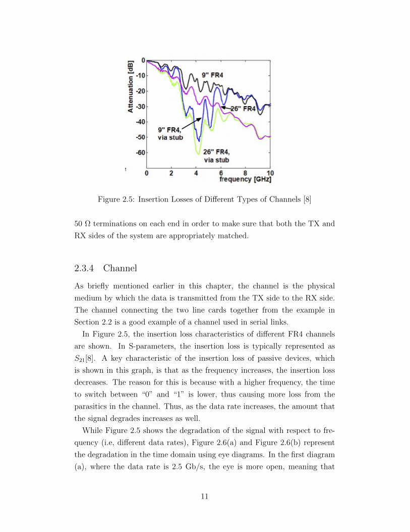
Figure 2.5: Insertion Losses of Different Types of Channels [8]
50 Ω terminations on each end in order to make sure that both the TX and
RX sides of the system are appropriately matched.
2.3.4 Channel
As briefly mentioned earlier in this chapter, the channel is the physical
medium by which the data is transmitted from the TX side to the RX side.
The channel connecting the two line cards together from the example in
Section 2.2 is a good example of a channel used in serial links.
In Figure 2.5, the insertion loss characteristics of different FR4 channels
are shown. In S-parameters, the insertion loss is typically represented as
S21[8]. A key characteristic of the insertion loss of passive devices, which
is shown in this graph, is that as the frequency increases, the insertion loss
decreases. The reason for this is because with a higher frequency, the time
to switch between “0” and “1” is lower, thus causing more loss from the
parasitics in the channel. Thus, as the data rate increases, the amount that
the signal degrades increases as well.
While Figure 2.5 shows the degradation of the signal with respect to fre-
quency (i.e, different data rates), Figure 2.6(a) and Figure 2.6(b) represent
the degradation in the time domain using eye diagrams. In the first diagram
(a), where the data rate is 2.5 Gb/s, the eye is more open, meaning that
11
it is easier to distinguish between “0” and “1” signal levels, and that there
is enough of a window to sample the signal (which is better represented by
the rectangle in the center). In the second diagram (b), the signal is barely
open, and as a result, there is little difference between a “0” and “1”, and the
sampling window is significantly less than the period of the bit itself. This
will drastically increase the bit error rate on the receiver end, making this a
terrible high speed serial link (HSSL). The effects shown in (b) are a result of
many different factors: insertion loss, reflected voltages, ISI, and dispersion.
With all of these effects, a SERDES system needs a module to counteract
these effects and clean up the signal.
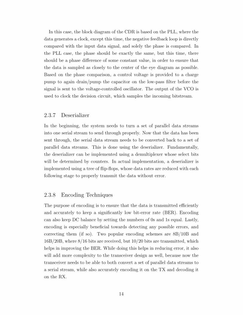
2.3.5 Equalizer
As shown in Figure 2.6(b), there are many physical characteristics of the
channel that contribute to the closed nature of the eye diagram. As a re-
sult, it is necessary to have something in the system to negate those effects.
Equalization at the TX end, RX end, or even both, is generally used to
reduce these effects and significantly increase the bit error rate. There are
multiple ways to equalize the received signal, two of which are shown in
Figure 2.7(a) and (b). In (a), the high frequencies are boosted, and in (b)
the lower frequencies are suppressed. In the case of (a), boosting the higher
frequencies accounts for the larger insertion loss at that rate. In the case of
(b), suppressing the lower frequencies reduces their levels without altering
any of the high frequency components. Both result in open eye diagrams
after being applied to the 5 Gb/s output shown previously [9]. Chapters 3-5
will further discuss the theory behind equalization, along with two different
methods used to equalize signals (with results to justify usage).
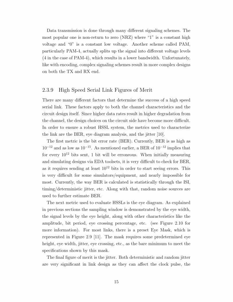
2.3.6 Clock and Data Recovery (CDR)
After the data is properly equalized and received, it is then fed through the
clock and data recovery (CDR) circuit. The TX clock is not used on the RX
side. Instead, the RX clock is generated based on the received bitstream and
used to sample the data stream as well. The block diagram representation
of a CDR is shown in Figure 2.8.
12
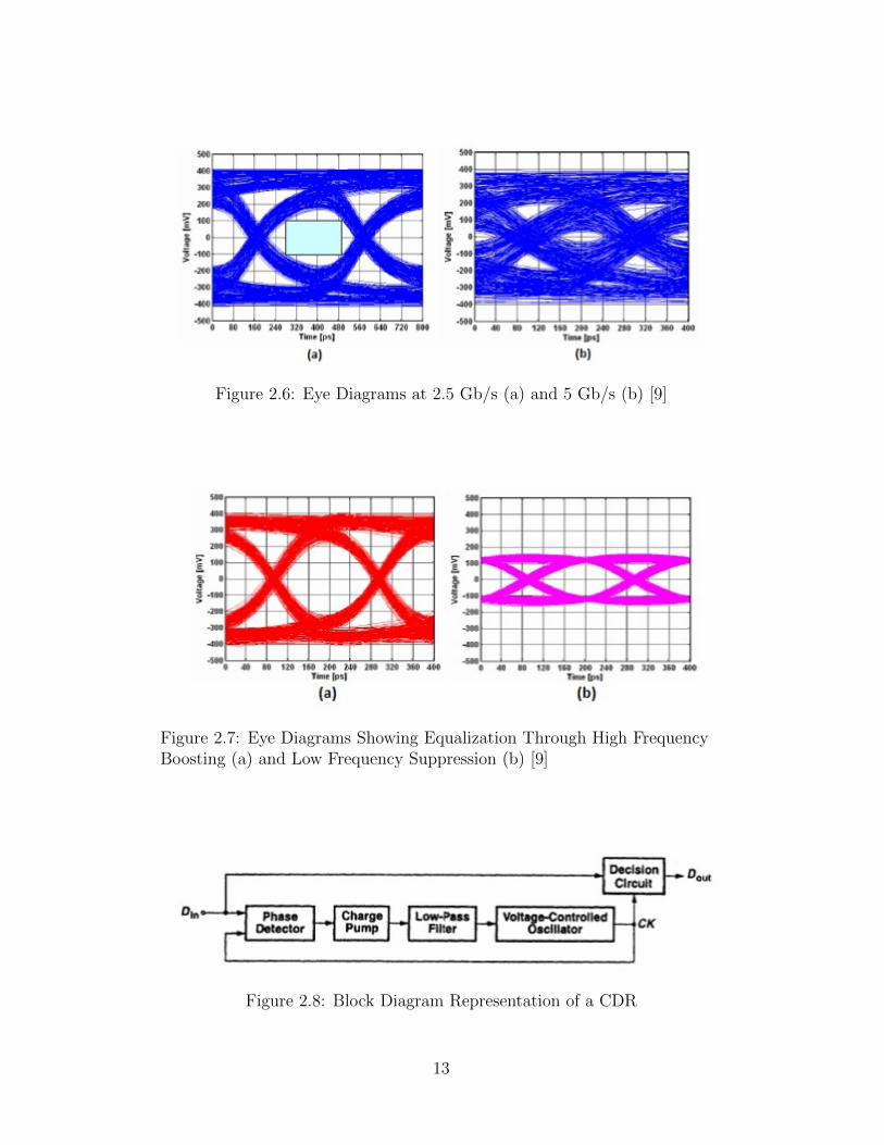
Figure 2.6: Eye Diagrams at 2.5 Gb/s (a) and 5 Gb/s (b) [9]
Figure 2.7: Eye Diagrams Showing Equalization Through High FrequencyBoosting (a) and Low Frequency Suppression (b) [9]
Figure 2.8: Block Diagram Representation of a CDR
13
In this case, the block diagram of the CDR is based on the PLL, where the
data generates a clock, except this time, the negative feedback loop is directly
compared with the input data signal, and solely the phase is compared. In
the PLL case, the phase should be exactly the same, but this time, there
should be a phase difference of some constant value, in order to ensure that
the data is sampled as closely to the center of the eye diagram as possible.
Based on the phase comparison, a control voltage is provided to a charge
pump to again drain/pump the capacitor on the low-pass filter before the
signal is sent to the voltage-controlled oscillator. The output of the VCO is
used to clock the decision circuit, which samples the incoming bitstream.
2.3.7 Deserializer
In the beginning, the system needs to turn a set of parallel data streams
into one serial stream to send through properly. Now that the data has been
sent through, the serial data stream needs to be converted back to a set of
parallel data streams. This is done using the deserializer. Fundamentally,
the deserializer can be implemented using a demultiplexer whose select bits
will be determined by counters. In actual implementation, a deserializer is
implemented using a tree of flip-flops, whose data rates are reduced with each
following stage to properly transmit the data without error.
2.3.8 Encoding Techniques
The purpose of encoding is to ensure that the data is transmitted efficiently
and accurately to keep a significantly low bit-error rate (BER). Encoding
can also keep DC balance by setting the numbers of 0s and 1s equal. Lastly,
encoding is especially beneficial towards detecting any possible errors, and
correcting them (if so). Two popular encoding schemes are 8B/10B and
16B/20B, where 8/16 bits are received, but 10/20 bits are transmitted, which
helps in improving the BER. While doing this helps in reducing error, it also
will add more complexity to the transceiver design as well, because now the
transceiver needs to be able to both convert a set of parallel data streams to
a serial stream, while also accurately encoding it on the TX and decoding it
on the RX.
14
Data transmission is done through many different signaling schemes. The
most popular one is non-return to zero (NRZ) where “1” is a constant high
voltage and “0” is a constant low voltage. Another scheme called PAM,
particularly PAM-4, actually splits up the signal into different voltage levels
(4 in the case of PAM-4), which results in a lower bandwidth. Unfortunately,
like with encoding, complex signaling schemes result in more complex designs
on both the TX and RX end.
2.3.9 High Speed Serial Link Figures of Merit
There are many different factors that determine the success of a high speed
serial link. These factors apply to both the channel characteristics and the
circuit design itself. Since higher data rates result in higher degradation from
the channel, the design choices on the circuit side have become more difficult.
In order to ensure a robust HSSL system, the metrics used to characterize
the link are the BER, eye diagram analysis, and the jitter [10].
The first metric is the bit error rate (BER). Currently, BER is as high as
10−12 and as low as 10−15. As mentioned earlier, a BER of 10−12 implies that
for every 1012 bits sent, 1 bit will be erroneous. When initially measuring
and simulating designs via EDA toolsets, it is very difficult to check for BER,
as it requires sending at least 1012 bits in order to start seeing errors. This
is very difficult for some simulators/equipment, and nearly impossible for
most. Currently, the way BER is calculated is statistically through the ISI,
timing/deterministic jitter, etc. Along with that, random noise sources are
used to further estimate BER.
The next metric used to evaluate HSSLs is the eye diagram. As explained
in previous sections the sampling window is demonstrated by the eye width,
the signal levels by the eye height, along with other characteristics like the
amplitude, bit period, eye crossing percentage, etc. (see Figure 2.10 for
more information). For most links, there is a preset Eye Mask, which is
represented in Figure 2.9 [11]. The mask requires some predetermined eye
height, eye width, jitter, eye crossing, etc., as the bare minimum to meet the
specifications shown by this mask.
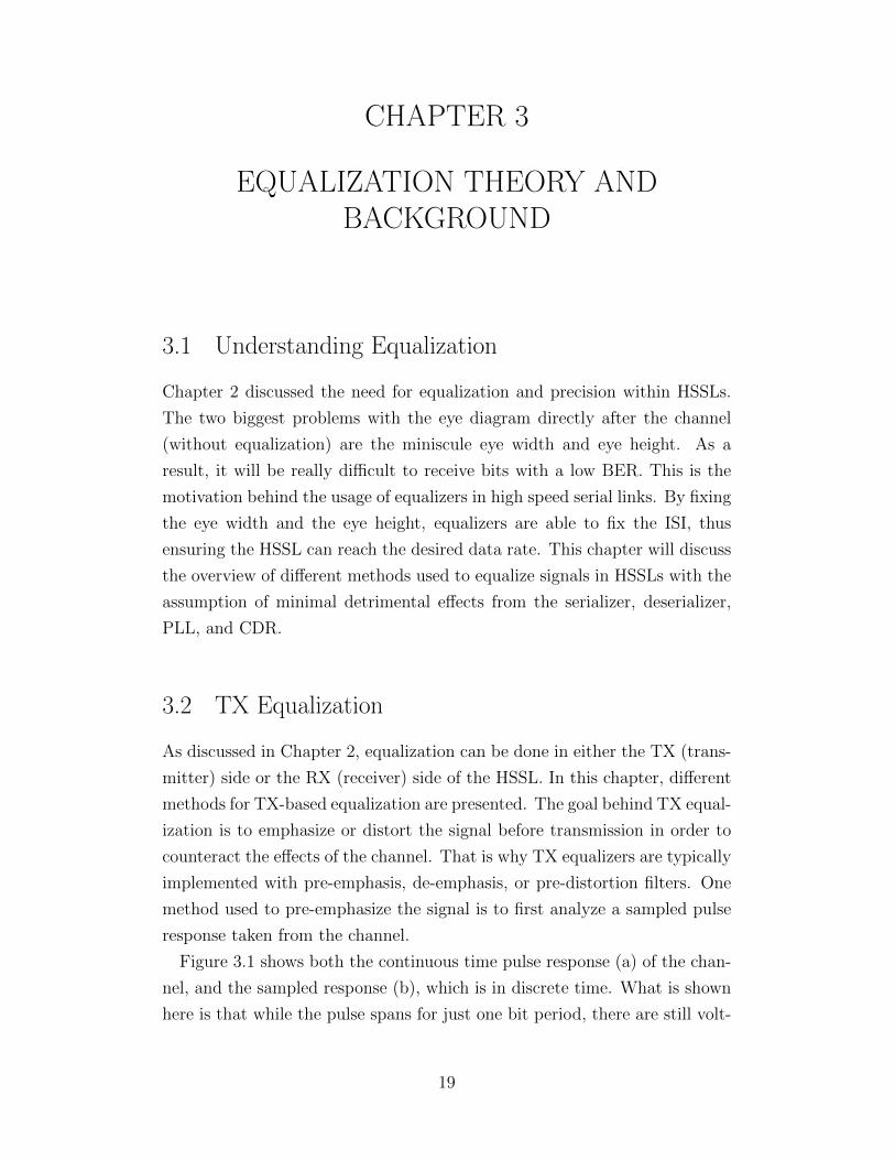
The final figure of merit is the jitter. Both deterministic and random jitter
are very significant in link design as they can affect the clock pulse, the
15
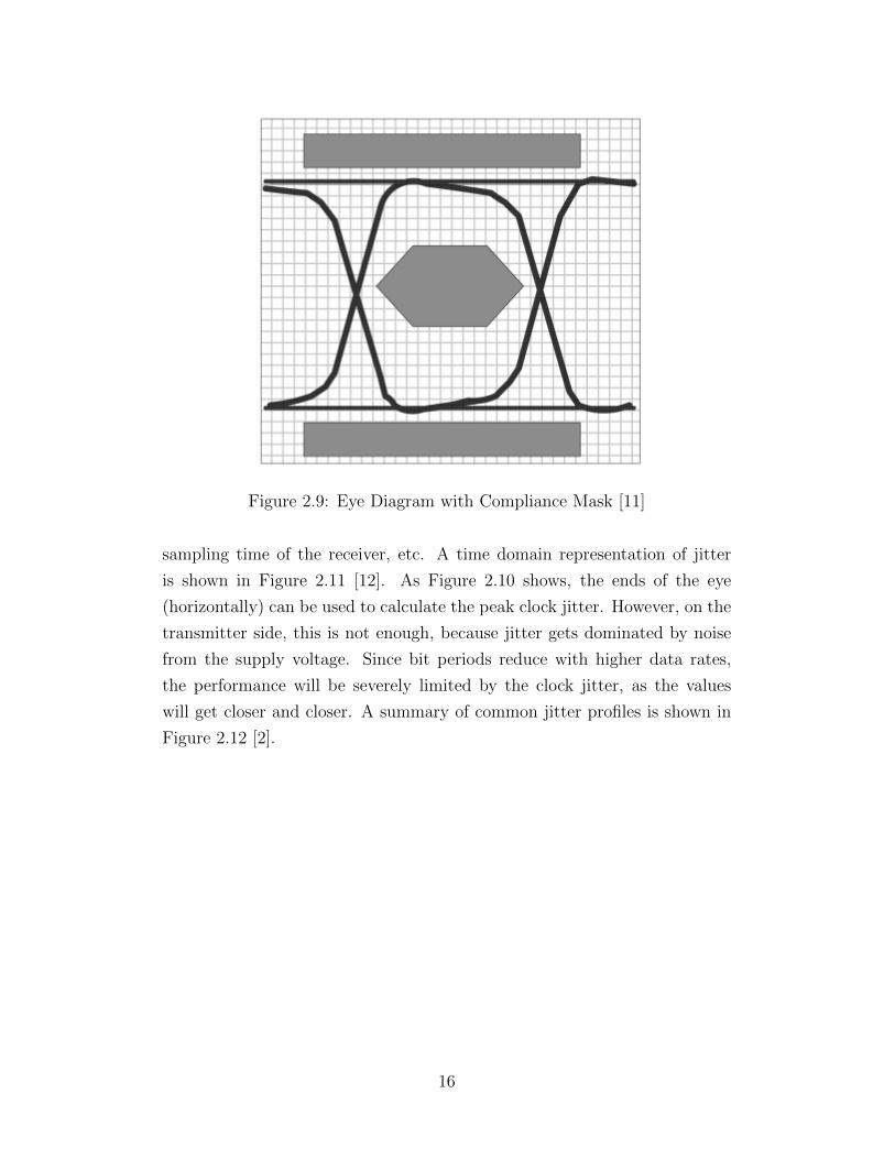
Figure 2.9: Eye Diagram with Compliance Mask [11]
sampling time of the receiver, etc. A time domain representation of jitter
is shown in Figure 2.11 [12]. As Figure 2.10 shows, the ends of the eye
(horizontally) can be used to calculate the peak clock jitter. However, on the
transmitter side, this is not enough, because jitter gets dominated by noise
from the supply voltage. Since bit periods reduce with higher data rates,
the performance will be severely limited by the clock jitter, as the values
will get closer and closer. A summary of common jitter profiles is shown in
Figure 2.12 [2].
16
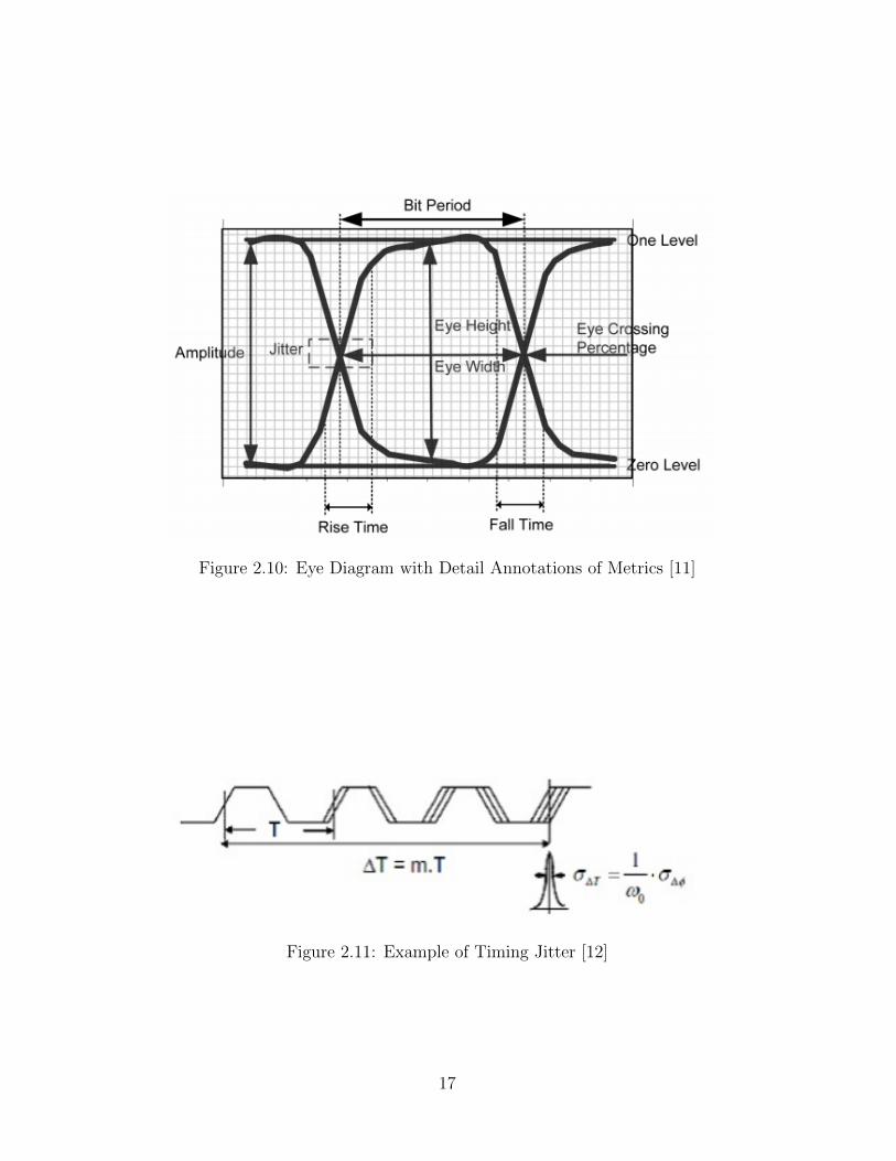
Figure 2.10: Eye Diagram with Detail Annotations of Metrics [11]
Figure 2.11: Example of Timing Jitter [12]
17
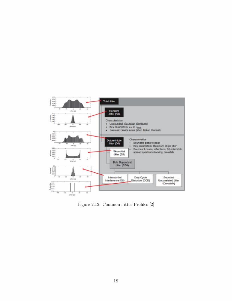
Figure 2.12: Common Jitter Profiles [2]
18
CHAPTER 3
EQUALIZATION THEORY ANDBACKGROUND
3.1 Understanding Equalization
Chapter 2 discussed the need for equalization and precision within HSSLs.
The two biggest problems with the eye diagram directly after the channel
(without equalization) are the miniscule eye width and eye height. As a
result, it will be really difficult to receive bits with a low BER. This is the
motivation behind the usage of equalizers in high speed serial links. By fixing
the eye width and the eye height, equalizers are able to fix the ISI, thus
ensuring the HSSL can reach the desired data rate. This chapter will discuss
the overview of different methods used to equalize signals in HSSLs with the
assumption of minimal detrimental effects from the serializer, deserializer,
PLL, and CDR.
3.2 TX Equalization
As discussed in Chapter 2, equalization can be done in either the TX (trans-
mitter) side or the RX (receiver) side of the HSSL. In this chapter, different
methods for TX-based equalization are presented. The goal behind TX equal-
ization is to emphasize or distort the signal before transmission in order to
counteract the effects of the channel. That is why TX equalizers are typically
implemented with pre-emphasis, de-emphasis, or pre-distortion filters. One
method used to pre-emphasize the signal is to first analyze a sampled pulse
response taken from the channel.
Figure 3.1 shows both the continuous time pulse response (a) of the chan-
nel, and the sampled response (b), which is in discrete time. What is shown
here is that while the pulse spans for just one bit period, there are still volt-
19
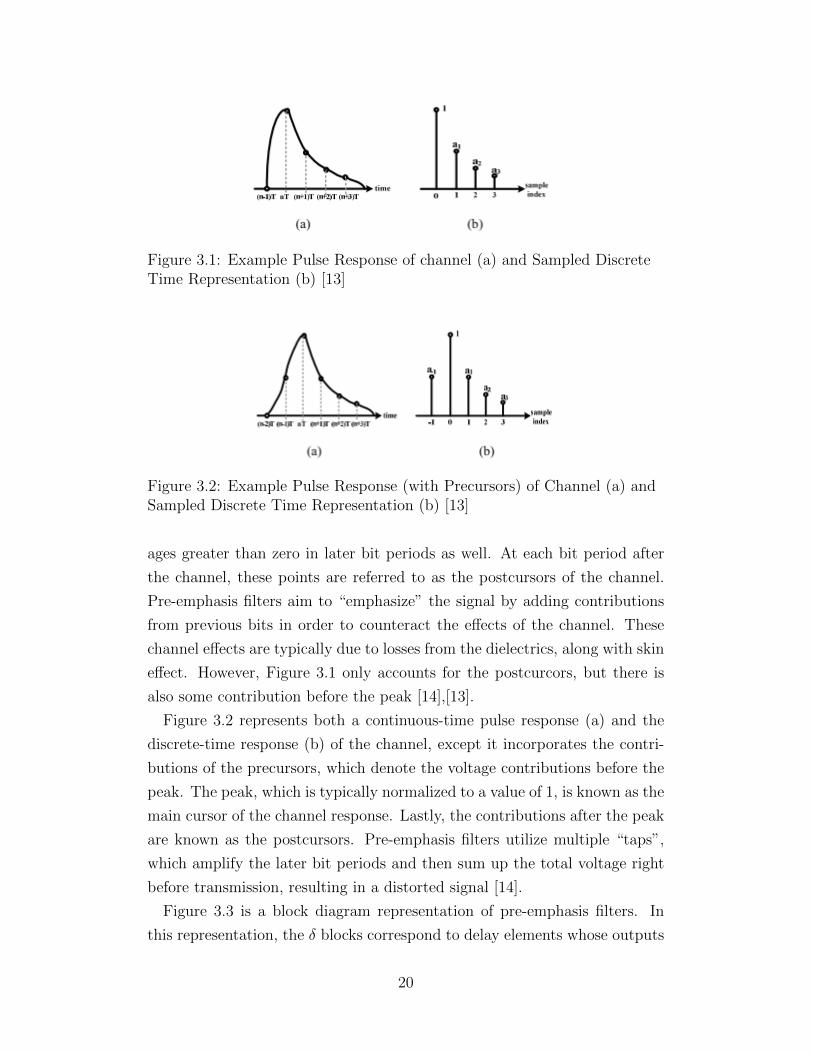
Figure 3.1: Example Pulse Response of channel (a) and Sampled DiscreteTime Representation (b) [13]
Figure 3.2: Example Pulse Response (with Precursors) of Channel (a) andSampled Discrete Time Representation (b) [13]
ages greater than zero in later bit periods as well. At each bit period after
the channel, these points are referred to as the postcursors of the channel.
Pre-emphasis filters aim to “emphasize” the signal by adding contributions
from previous bits in order to counteract the effects of the channel. These
channel effects are typically due to losses from the dielectrics, along with skin
effect. However, Figure 3.1 only accounts for the postcurcors, but there is
also some contribution before the peak [14],[13].
Figure 3.2 represents both a continuous-time pulse response (a) and the
discrete-time response (b) of the channel, except it incorporates the contri-
butions of the precursors, which denote the voltage contributions before the
peak. The peak, which is typically normalized to a value of 1, is known as the
main cursor of the channel response. Lastly, the contributions after the peak
are known as the postcursors. Pre-emphasis filters utilize multiple “taps”,
which amplify the later bit periods and then sum up the total voltage right
before transmission, resulting in a distorted signal [14].
Figure 3.3 is a block diagram representation of pre-emphasis filters. In
this representation, the δ blocks correspond to delay elements whose outputs
20
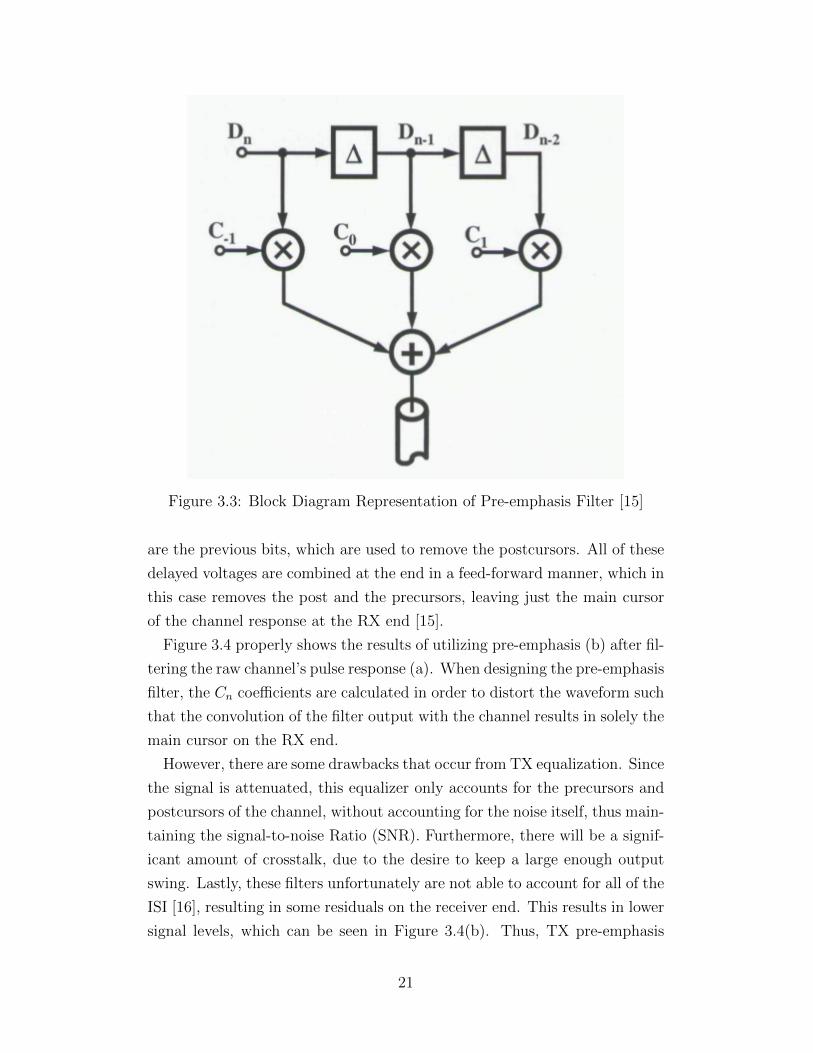
Figure 3.3: Block Diagram Representation of Pre-emphasis Filter [15]
are the previous bits, which are used to remove the postcursors. All of these
delayed voltages are combined at the end in a feed-forward manner, which in
this case removes the post and the precursors, leaving just the main cursor
of the channel response at the RX end [15].
Figure 3.4 properly shows the results of utilizing pre-emphasis (b) after fil-
tering the raw channel’s pulse response (a). When designing the pre-emphasis
filter, the Cn coefficients are calculated in order to distort the waveform such
that the convolution of the filter output with the channel results in solely the
main cursor on the RX end.
However, there are some drawbacks that occur from TX equalization. Since
the signal is attenuated, this equalizer only accounts for the precursors and
postcursors of the channel, without accounting for the noise itself, thus main-
taining the signal-to-noise Ratio (SNR). Furthermore, there will be a signif-
icant amount of crosstalk, due to the desire to keep a large enough output
swing. Lastly, these filters unfortunately are not able to account for all of the
ISI [16], resulting in some residuals on the receiver end. This results in lower
signal levels, which can be seen in Figure 3.4(b). Thus, TX pre-emphasis
21
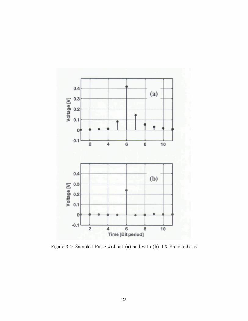
Figure 3.4: Sampled Pulse without (a) and with (b) TX Pre-emphasis
22
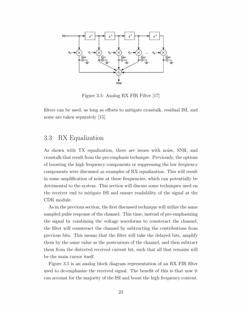
Figure 3.5: Analog RX FIR Filter [17]
filters can be used, as long as efforts to mitigate crosstalk, residual ISI, and
noise are taken separately [15].
3.3 RX Equalization
As shown with TX equalization, there are issues with noise, SNR, and
crosstalk that result from the pre-emphasis technique. Previously, the options
of boosting the high frequency components or suppressing the low frequency
components were discussed as examples of RX equalization. This will result
in some amplification of noise at these frequencies, which can potentially be
detrimental to the system. This section will discuss some techniques used on
the receiver end to mitigate ISI and ensure readability of the signal at the
CDR module.
As in the previous section, the first discussed technique will utilize the same
sampled pulse response of the channel. This time, instead of pre-emphasizing
the signal by combining the voltage waveforms to counteract the channel,
the filter will counteract the channel by subtracting the contributions from
previous bits. This means that the filter will take the delayed bits, amplify
them by the same value as the postcursors of the channel, and then subtract
them from the distorted received current bit, such that all that remains will
be the main cursor itself.
Figure 3.5 is an analog block diagram representation of an RX FIR filter
used to de-emphasize the received signal. The benefit of this is that now it
can account for the majority of the ISI and boost the high frequency content.
23
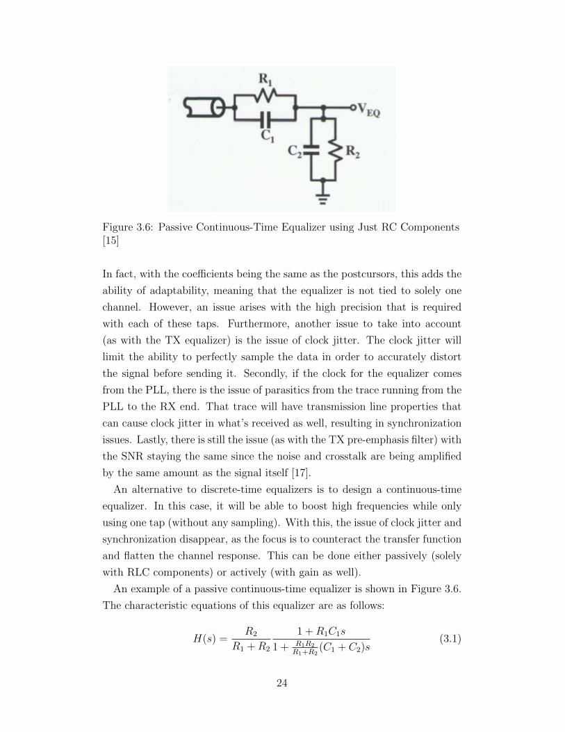
Figure 3.6: Passive Continuous-Time Equalizer using Just RC Components[15]
In fact, with the coefficients being the same as the postcursors, this adds the
ability of adaptability, meaning that the equalizer is not tied to solely one
channel. However, an issue arises with the high precision that is required
with each of these taps. Furthermore, another issue to take into account
(as with the TX equalizer) is the issue of clock jitter. The clock jitter will
limit the ability to perfectly sample the data in order to accurately distort
the signal before sending it. Secondly, if the clock for the equalizer comes
from the PLL, there is the issue of parasitics from the trace running from the
PLL to the RX end. That trace will have transmission line properties that
can cause clock jitter in what’s received as well, resulting in synchronization
issues. Lastly, there is still the issue (as with the TX pre-emphasis filter) with
the SNR staying the same since the noise and crosstalk are being amplified
by the same amount as the signal itself [17].
An alternative to discrete-time equalizers is to design a continuous-time
equalizer. In this case, it will be able to boost high frequencies while only
using one tap (without any sampling). With this, the issue of clock jitter and
synchronization disappear, as the focus is to counteract the transfer function
and flatten the channel response. This can be done either passively (solely
with RLC components) or actively (with gain as well).
An example of a passive continuous-time equalizer is shown in Figure 3.6.
The characteristic equations of this equalizer are as follows:
H(s) =R2
R1 +R2
1 +R1C1s
1 + R1R2
R1+R2(C1 + C2)s
(3.1)
24
ωz =1
R1C1
(3.2)
ωp =1
R1R2
R1+R2(C1 + C2)
(3.3)
DC Gain =R2
R1 +R2
(3.4)
The utilization of this RC network will result in high frequency boosting
by attenuating the low frequency components via the resistors and boosting
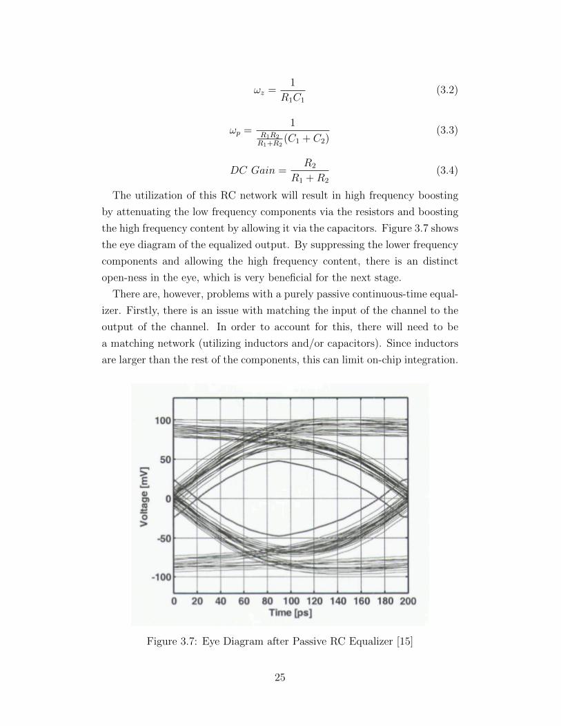
the high frequency content by allowing it via the capacitors. Figure 3.7 shows
the eye diagram of the equalized output. By suppressing the lower frequency
components and allowing the high frequency content, there is an distinct
open-ness in the eye, which is very beneficial for the next stage.
There are, however, problems with a purely passive continuous-time equal-
izer. Firstly, there is an issue with matching the input of the channel to the
output of the channel. In order to account for this, there will need to be
a matching network (utilizing inductors and/or capacitors). Since inductors
are larger than the rest of the components, this can limit on-chip integration.
Figure 3.7: Eye Diagram after Passive RC Equalizer [15]
25

Lastly, this will scale down both signal and noise, resulting in no change in
SNR. Thus, this is not a practical use case for HSSLs [15]. Chapter 5 discusses
an active CTLE topology, the design process behind its implementation, and
simulated results using Cadence Spectre.
26
CHAPTER 4
FFE DESIGN AND IMPLEMENTATION
Chapter 3 discussed the pre-emphasis filtering technique for TX equalization
with the feed-forward equalizer (FFE). “Feed-forward” denotes the method
by which the current bit and the delay blocks are distorted, and then added
together at the end before transmission. This is contrary to the feedback
method, which was discussed in the RX FIR filter technique, where the
distorted delayed signals get combined and then subtracted from the current
bit in order to remove the postcursors of the channel. The advantage of
the TX feed-forward method is that it accounts for both postcursors and
precursors, whereas with the RX feedback method, it eliminates more of
the ISI. This chapter discusses the design process for implementing an FFE,
along with presenting the results for a behavioral implementation of a 2-Tap
FFE meant to eliminate solely the precursor.
4.1 FFE Design Overview
The implementation of a 5-tap behavioral feed-forward equalizer (FFE) is
done via this design process:
1. Analyze the normalized pulse response to find the main cursor, the
precursor, and the post-cursors.
2. Using the values of the main cursor, precursor, and postcursors (a-
coefficients), find the factors for the FFE (b-coefficients) to distort the
signal such that only the main cursor is at the output. This is mathe-
matically represented by the equation
A× b = c (4.1)
27
where A, b, and c are represented as (respectively):a0 a−1 0 0 0
a1 a0 a−1 0 0
a2 a1 a0 a−1 0
a3 a2 a1 a0 a−1
0 a3 a2 a1 a0
×b−1
b0
b1
b2
b3
=
0
1
0
0
0
(4.2)
From this, the equation to solve for the FFE coefficients is simply:
b = A−1c [13].
3. Test the FFE-coefficients mathematically by convolving the b-matrix
with the A-matrix and check that there is solely the main cursor at the
output.
4. Design the behavioral model of the FFE using Verilog-AMS and verify
successful compilation.
5. Set up and simulate a testbench on EDA (Electronic Design Automa-
tion) tools (like Cadence Virtuoso + Spectre) and verify the output
voltage waveform entering the RX end after placing the FFE before
the channel.
4.2 FFE Implementation and Results
There are three modifications that are made to this design process in the
presented FFE implementation:
1. The presented FFE only focuses on eliminating the precursor, thus
instead of an A-matrix with a width of 5, it is reduced to a width of
2, as the b matrix is now reduced to a height of 2 (only solving for b−1
and b0).
2. In order to account for as much ISI as possible, the heights of matrix
A and c are increased, meaning that the pulse response of the channel
is taken to a length of over 1000 unit intervals (UI), where in this case,
a UI is equivalent to one bit period. This means that in solving for
28
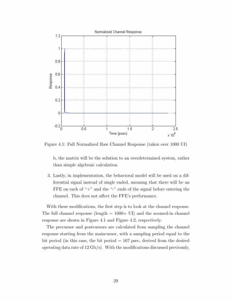
Figure 4.1: Full Normalized Raw Channel Response (taken over 1000 UI)
b, the matrix will be the solution to an overdetermined system, rather
than simple algebraic calculation.
3. Lastly, in implementation, the behavioral model will be used on a dif-
ferential signal instead of single ended, meaning that there will be an
FFE on each of “+” and the “-” ends of the signal before entering the
channel. This does not affect the FFE’s performance.
With these modifications, the first step is to look at the channel response.
The full channel response (length = 1000+ UI) and the zoomed-in channel
response are shown in Figure 4.1 and Figure 4.2, respectively.
The precursor and postcursors are calculated from sampling the channel
response starting from the maincursor, with a sampling period equal to the
bit period (in this case, the bit period = 167 psec, derived from the desired
operating data rate of 12 Gb/s). With the modifications discussed previously,
29
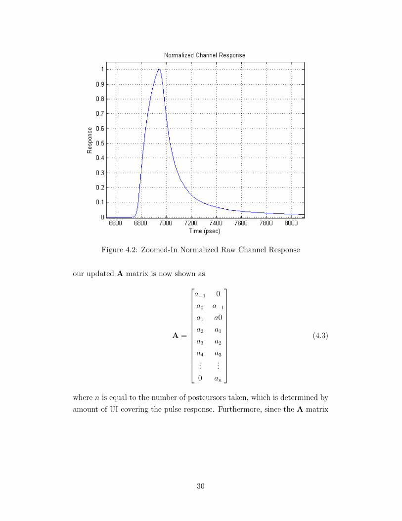
Figure 4.2: Zoomed-In Normalized Raw Channel Response
our updated A matrix is now shown as
A =
a−1 0
a0 a−1
a1 a0
a2 a1
a3 a2
a4 a3...
...
0 an
(4.3)
where n is equal to the number of postcursors taken, which is determined by
amount of UI covering the pulse response. Furthermore, since the A matrix
30
extends back one more bit period, our updated c matrix is now shown as
c =
0
0
1
0...
0
(4.4)
Using the raw channel response, our cursors are
Precursor a−1 = 0.1109 (4.5)
Postcursor a1 = 0.2605 (4.6)
Postcursor a2 = 0.104 (4.7)
Postcursor a3 = 0.0588 (4.8)
Postcursor a4 = 0.0387 (4.9)
Postcursor a5 = 0.0284 (4.10)
.
Beyond these, the values are significantly lower, where the final postcursor
an = 9.896× 10⁻⁶. As previously mentioned, sampling over a longer channel
response helps in reducing more ISI.
The next step is to invert the updated A matrix and multiply with the
updated c matrix. In solving this overdetermined system, the solution for b
matrix is
b = A−1 × c =
[−0.1193
0.9549
](4.11)
In actual implementation, the coefficients are used as multipliers towards
the current used in differential amplifiers, where the current sources in each
tap draw some amount of current in order to distort the output voltage.
With this circuit topology, which is shown in Figure 4.3, the output swing is
limited by the headroom of the design itself [15]. This means that any extra
taps that are added to this equalizer will result in a reduction of the cursor’s
31
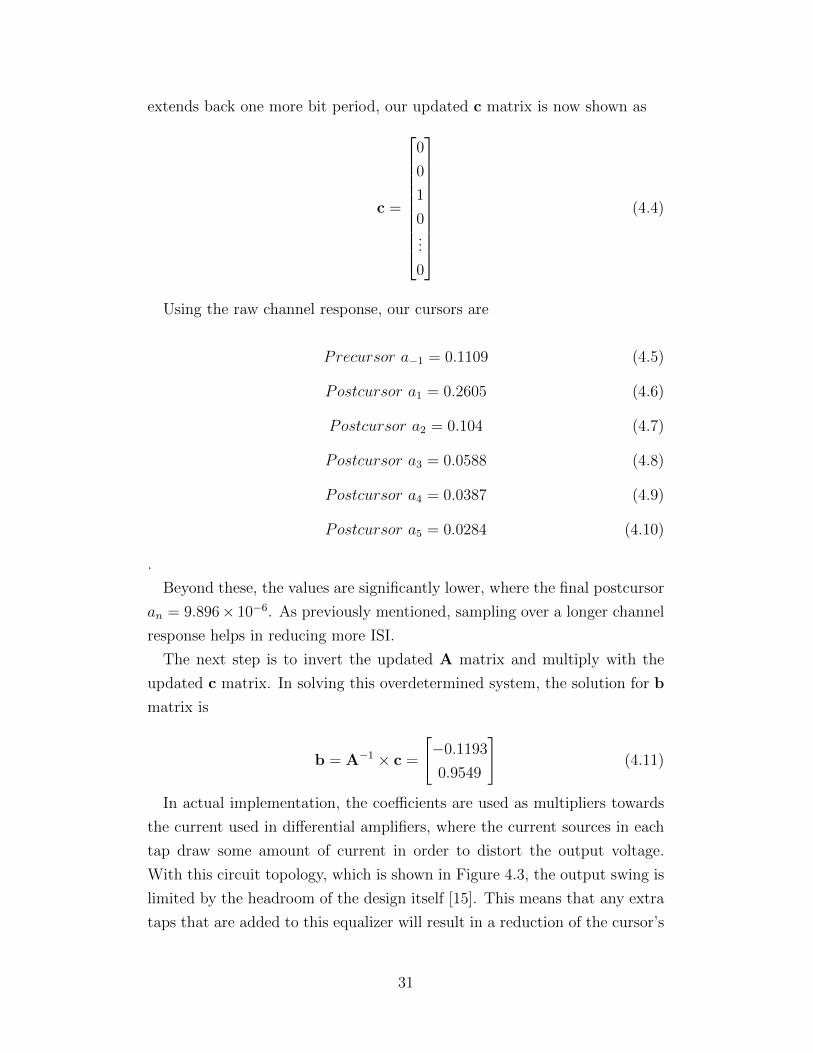
Figure 4.3: Circuit Topology of 2-Tap FFE[15]
tap weight. Because of this, the sum of currents from each tap needs to be
equal to the current across the output termination, meaning that:
I × Σ|bi| = I ⇒ Σ|bi| = 1 (4.12)
With this realization, the normalized FFE coefficients are now:
bnew =b
|b|=
[−0.111
0.889
](4.13)
The next step is to mathematically test these coefficients by convolving
the new b matrix with the sampled raw channel response in order to see if
the precursor is successfully eliminated. See Figure 4.4. The precursor has
been properly reduced, resulting in a slight reduction in the main cursor as
well. With the utilization of a driver amp and either further taps on the FFE
or an RX FIR filter, the signal will be at the appropriate voltage levels, and
the postcursors will be eliminated.
The next step is to implement this behaviorally on a testbench. As dis-
cussed in previous chapters, this thesis utilizes the Cadence toolset to imple-
32
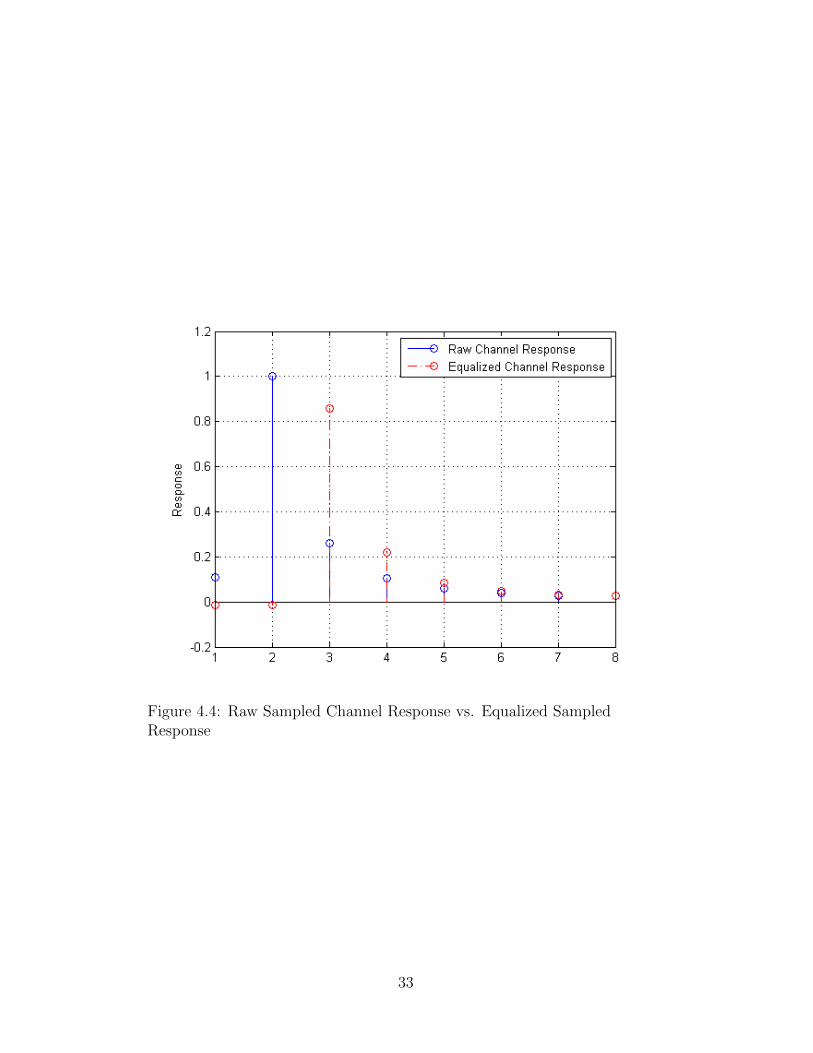
Figure 4.4: Raw Sampled Channel Response vs. Equalized SampledResponse
33
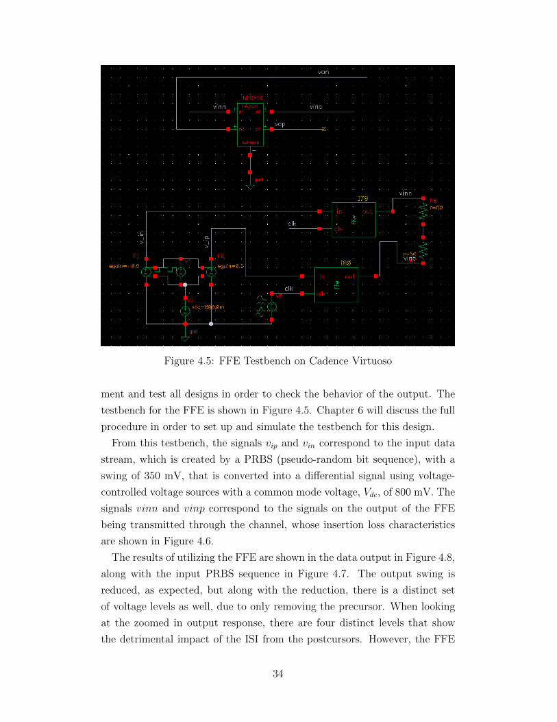
Figure 4.5: FFE Testbench on Cadence Virtuoso
ment and test all designs in order to check the behavior of the output. The
testbench for the FFE is shown in Figure 4.5. Chapter 6 will discuss the full
procedure in order to set up and simulate the testbench for this design.
From this testbench, the signals vip and vin correspond to the input data
stream, which is created by a PRBS (pseudo-random bit sequence), with a
swing of 350 mV, that is converted into a differential signal using voltage-
controlled voltage sources with a common mode voltage, Vdc, of 800 mV. The
signals vinn and vinp correspond to the signals on the output of the FFE
being transmitted through the channel, whose insertion loss characteristics
are shown in Figure 4.6.
The results of utilizing the FFE are shown in the data output in Figure 4.8,
along with the input PRBS sequence in Figure 4.7. The output swing is
reduced, as expected, but along with the reduction, there is a distinct set
of voltage levels as well, due to only removing the precursor. When looking
at the zoomed in output response, there are four distinct levels that show
the detrimental impact of the ISI from the postcursors. However, the FFE
34
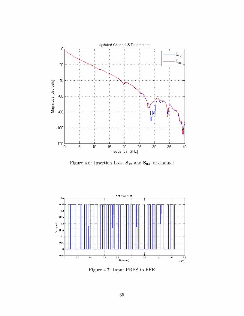
Figure 4.6: Insertion Loss, S12 and S34, of channel
Figure 4.7: Input PRBS to FFE
35
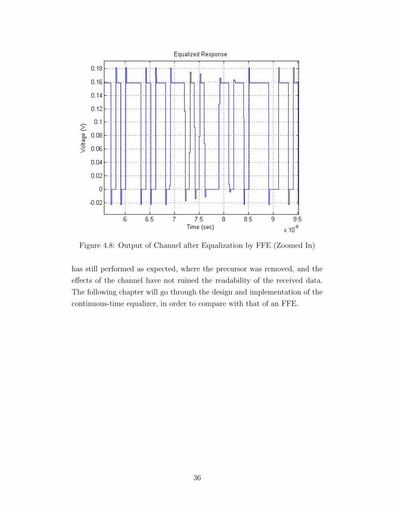
Figure 4.8: Output of Channel after Equalization by FFE (Zoomed In)
has still performed as expected, where the precursor was removed, and the
effects of the channel have not ruined the readability of the received data.
The following chapter will go through the design and implementation of the
continuous-time equalizer, in order to compare with that of an FFE.
36
CHAPTER 5
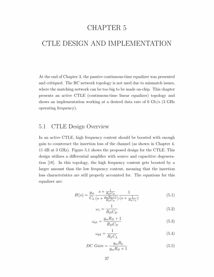
CTLE DESIGN AND IMPLEMENTATION
At the end of Chapter 3, the passive continuous-time equalizer was presented
and critiqued. The RC network topology is not used due to mismatch issues,
where the matching network can be too big to be made on-chip. This chapter
presents an active CTLE (continuous-time linear equalizer) topology and
shows an implementation working at a desired data rate of 6 Gb/s (3 GHz
operating frequency).
5.1 CTLE Design Overview
In an active CTLE, high frequency content should be boosted with enough
gain to counteract the insertion loss of the channel (as shown in Chapter 4,
11 dB at 3 GHz). Figure 5.1 shows the proposed design for the CTLE. This
design utilizes a differential amplifier with source and capacitive degenera-
tion [18]. In this topology, the high frequency content gets boosted by a
larger amount than the low frequency content, meaning that the insertion
loss characteristics are still properly accounted for. The equations for this
equalizer are:
H(s) =gmCL
s+ 1RDCD
(s+ gmRD+1RDCD
)
1
(s+ 1RLCL
)(5.1)
ωz =1
RDCD
(5.2)
ωp1 =gmRD + 1
RDCD
(5.3)
ωp2 =1
RLCL
(5.4)
DC Gain =gmRL
gmRD + 1(5.5)
37
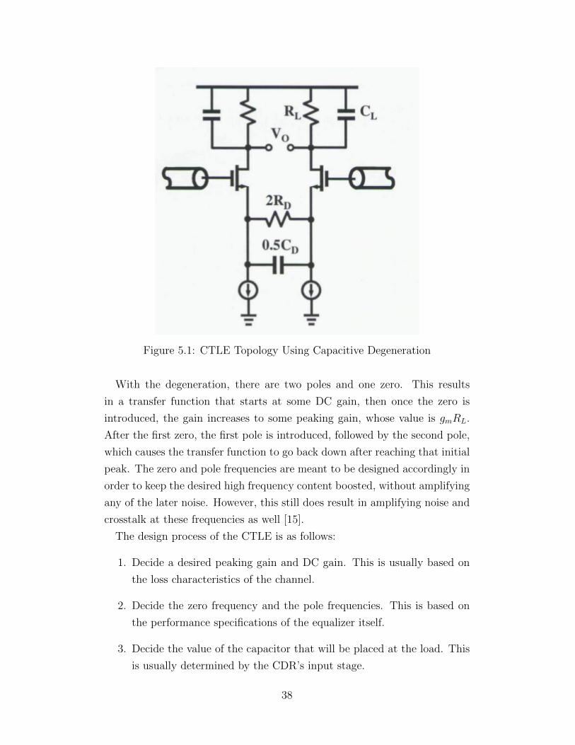
Figure 5.1: CTLE Topology Using Capacitive Degeneration
With the degeneration, there are two poles and one zero. This results
in a transfer function that starts at some DC gain, then once the zero is
introduced, the gain increases to some peaking gain, whose value is gmRL.
After the first zero, the first pole is introduced, followed by the second pole,
which causes the transfer function to go back down after reaching that initial
peak. The zero and pole frequencies are meant to be designed accordingly in
order to keep the desired high frequency content boosted, without amplifying
any of the later noise. However, this still does result in amplifying noise and
crosstalk at these frequencies as well [15].
The design process of the CTLE is as follows:
1. Decide a desired peaking gain and DC gain. This is usually based on
the loss characteristics of the channel.
2. Decide the zero frequency and the pole frequencies. This is based on
the performance specifications of the equalizer itself.
3. Decide the value of the capacitor that will be placed at the load. This
is usually determined by the CDR’s input stage.
38

4. Determine the output swing of the equalizer. This is generally deter-
mined by the input specifications of the CDR as well.
5. Calculate the appropriate biasing current, and the width and length of
the transistor, in order to satisfy the design equations for this differen-
tial amplifier.
6. Calculate the total load capacitance, which is typically based on the
load capacitor and the parasitics of the transistors.
7. Calculate the load resistance to satisfy pole frequency ωp2.
8. Calculate the degeneration resistance from the transconductance of the
amplifier with the ratio of the peaking gain and the DC gain. This is
found from the following equation:
RD =
Hpeak
HDC− 1
Gm
(5.6)
9. Calculate the degeneration capacitance to satisfy zero frequency ωz.
10. Test design and optimize parameters as necessary.
This design process from Step 5 onwards becomes iterative in order to
ensure that the CTLE properly accounts for the losses in the channel and
keeps the eye open enough for the CDR with minimal jitter.
5.2 CTLE Implementation and Results
For the scope of this research project, the design specs are as follows:
1. Operating Frequency = 3 GHz
2. CL = 30 fF
3. fp2 = 4 GHz
4. fz = 500 MHz
5. Peaking Gain = 10 dB
39
6. DC Gain = 7 dB
7. Output Swing = 300 mV
8. Vdd = 1.2 V
The design parameters for the CTLE circuit, after running through the
iterative design process, are:
1. W = 12.5 µm
2. L = 100 nm
3. Ibias = 250 µA
4. CD = 1.52 pF
5. RD = 209 Ω
6. RL = 1.2 kΩ
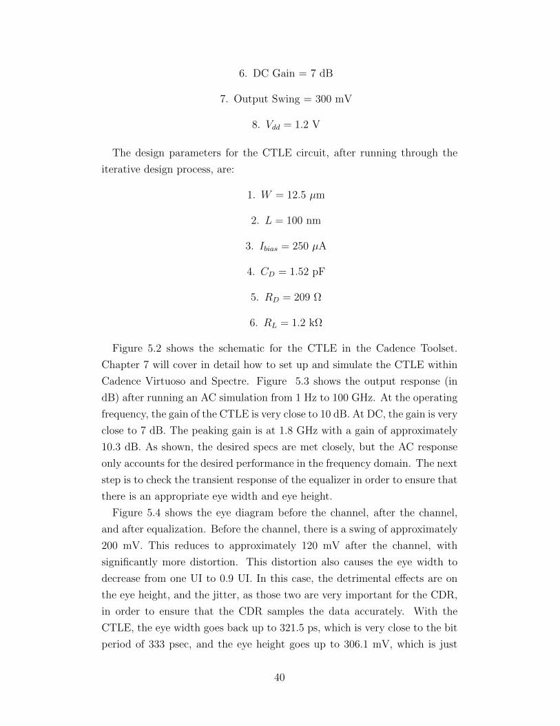
Figure 5.2 shows the schematic for the CTLE in the Cadence Toolset.
Chapter 7 will cover in detail how to set up and simulate the CTLE within
Cadence Virtuoso and Spectre. Figure 5.3 shows the output response (in
dB) after running an AC simulation from 1 Hz to 100 GHz. At the operating
frequency, the gain of the CTLE is very close to 10 dB. At DC, the gain is very
close to 7 dB. The peaking gain is at 1.8 GHz with a gain of approximately
10.3 dB. As shown, the desired specs are met closely, but the AC response
only accounts for the desired performance in the frequency domain. The next
step is to check the transient response of the equalizer in order to ensure that
there is an appropriate eye width and eye height.
Figure 5.4 shows the eye diagram before the channel, after the channel,
and after equalization. Before the channel, there is a swing of approximately
200 mV. This reduces to approximately 120 mV after the channel, with
significantly more distortion. This distortion also causes the eye width to
decrease from one UI to 0.9 UI. In this case, the detrimental effects are on
the eye height, and the jitter, as those two are very important for the CDR,
in order to ensure that the CDR samples the data accurately. With the
CTLE, the eye width goes back up to 321.5 ps, which is very close to the bit
period of 333 psec, and the eye height goes up to 306.1 mV, which is just
40
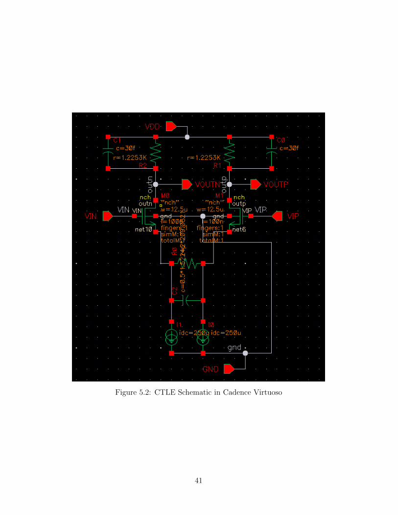
Figure 5.2: CTLE Schematic in Cadence Virtuoso
41
Figure 5.3: CTLE AC Response in Cadence Spectre
Figure 5.4: Eye Diagram before Channel (Yellow), after Channel (Green),and after Equalization (Red)
42
over our desired voltage swing. This means that the CDR will have enough
time to properly sample the data and can easily distinguish between a “0”
and a “1”. Lastly, the jitter reduces to 12.5 ps from the 65 ps of jitter it
reached after the channel. Overall, this CTLE performed as expected.
In conclusion, the CTLE provides the equalization needed to account for
both the losses and the slowed down transition times due to the channel.
Since it is operating in continuous-time, clock jitter and sampling do not
cause issues here. However, the limitations of the CTLE are shown in the
output swing and the gain. Since the CTLE is providing both gain and a large
output swing, it is difficult to accomplish that with small dimensions and
low power consumption. Due to that, the design process becomes iterative
in order to accomplish both high gain and output swing, as well as small size
and low power consumption.
Chapter 6 and Chapter 7 will provide tutorials for users to design their own
FFE, CTLE, and testbenches for both the behavioral model and transistor
model simulations.
43
CHAPTER 6
BEHAVIORAL LEVEL SIMULATION OFFFE
6.1 Overview of Behavioral Simulation
Chapter 4 discussed the design process behind a behavioral implementation
of an FFE. This chapter will provide a tutorial towards executing the design
process for an FFE.
There are two main types of implementations that are beneficial to do when
designing and testing circuits. SPICE (Simulation Program with Integrated
Circuit Emphasis) is traditionally the simulation engine base that is used
to simulate circuits, especially in the mixed-signal/analog realm. However,
as the circuits get more and more complex, so does the simulation time.
This results in fewer revisions by the designer. SPICE simulates the circuits
by performing a nodal analysis through KCL (Kirchhoff’s current law) at
every node. In the case of complex circuits, all of the KCL equations can
be represented through matrices (as they are a system of equations). The
solutions to the equations will require matrix inversion, which will have a
computational complexity of at least O(n2). Thus, the computation time will
rapidly increase with the increasing number of nodes. Behavioral modeling
serves the purpose of testing functionality while significantly reducing the
number of nodes and in turn, reducing the simulation time.
In the case of complex systems, the simulation time is significantly faster,
as there are no computationally complex operations during performance.
Furthermore, behavioral modeling allows for testing different systems itera-
tively. This allows for significantly faster optimization time, which is espe-
cially beneficial in the case of the FFE tap coefficients. Since these models
work in SPICE simulations, the same testbench can be utilized in both be-
havioral and transistor-level testing. This also enables quickly re-running
tests after simply changing parameter values, where in transistor-level sim-
44
ulations, much of the circuit would need to be redesigned in order to meet
the new design parameter. Lastly, as different technology is used, the whole
transistor-level circuit will need to be re-designed, whereas behavioral models
are simply re-allocated by changing the design parameters.
The behavioral models for mixed-signal simulations are written in Verilog-
AMS (Verilog-Analog Mixed-Signal). This language defines both the behav-
ior and the structure for analog and mixed signal systems. Originally, be-
havioral modeling was typically done using just Verilog or VHDL, but these
two languages are meant specifically for digital circuits. Verilog-AMS is an
extension to these hardware description languages (HDLs) that provides the
designer with the ability to prototype their systems much faster, allowing
for quicker optimization. Verilog-AMS provides a language and simulator
ecosystem to be shared between analog, digital, and system level design, giv-
ing it a key advantage. By utilizing the speed and capacity of Verilog, along
with its own event-driven capabilities, Verilog-AMS provides the user with
the ability to easily simulate and optimize complex systems, such as PLLs,
CDRs, DFEs (Decision Feedback Equalizers), ADCs, and much more. How-
ever, Verilog-AMS does not have synthesis capabilities like Verilog, so it is
still not a replacement for transistor-level modeling. It is strictly meant to
speed up initial testing and optimization.
In this simulation, the Cadence toolset is used for simulation, as its Verilog-
AMS simulator works with both Verilog-D and Verilog-A models as well. Fur-
thermore, it operates cohesively with Spectre, Cadence’s tool for transistor-
level simulation. An example of a Verilog-AMS model, implementing a D-
type flip-flop, is shown in Figure 6.1.
The “disciplines.vams” file that is included in the beginning of the file
defines the signal types that are used in Verilog-AMS. These are typically
referred to as “natures”. The signals of the block itself are defined within
the parentheses of the module. In this case, the parentheses contain signals
”q”, ”qb”, ”clk”, and ”d”. These are the output, inverted output, clock, and
input, respectively. The input/output classifiers are set within the module’s
code itself (there is also a third type known as inout, which is typically used
in bi-directional digital communication buses). The parameter real classifier
is used to signify parameters whose value will be set externally within the
simulator. In Cadence, when the block is created, the user has to edit the
properties of the block and set the values before successfully simulating it.
45
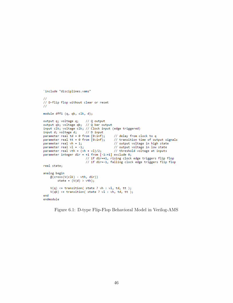
Figure 6.1: D-type Flip-Flop Behavioral Model in Verilog-AMS
46
The “analog begin” signifies when the simulator should start modeling this
block. Lastly, the “endmodule” is used to signify when the compiler should
stop compiling the code within the module’s role in the simulation.
6.2 FFE Behavioral Model Setup
In Chapter 4, the design process towards calculating the FFE was presented.
As a result of the design process, the FFE’s coefficients (designed to eliminate
solely the precursor) were:
b =
[−0.111
0.889
](6.1)
Following this is the process towards setting up the behavioral model and
simulating it with a testbench:
1. First, create a new library that you will use to create your symbol,
testbench, etc., for your behavioral model simulation. In this case, we
will call our library FFE-Demo. Properly setting it up is shown in
Figure 6.2. When setting it up, attach it to an existing technology. In
this case, use the TSMC65N technology, as the 65 nm technology is
the basis behind all of the designs in this project.
2. The next step is to create the Verilog-AMS model for the FFE. To do
this, we must first create the cellview for this by going to “File...New...Cell
View” and inputting the parameters as shown in Figure 6.3.
3. After hitting “Ok”, there will be a text editor popup that will be black,
as shown in Figure 6.4. Fill in the skeleton code with the code shown
in Figure 6.5
4. Once completed, hit “Save” and exit the Text Editor. After doing this,
a pop-up will ask if you would like to create a symbol for this file. Click
“Yes”, as you need this symbol to be placed into the FFE testbench. In
this case, our symbol appears as shown in Figure 6.6, where the inputs
are on the left side and the outputs are on the right. Now, we have a
completed FFE behavioral model.
47
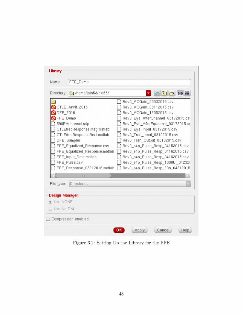
Figure 6.2: Setting Up the Library for the FFE
48
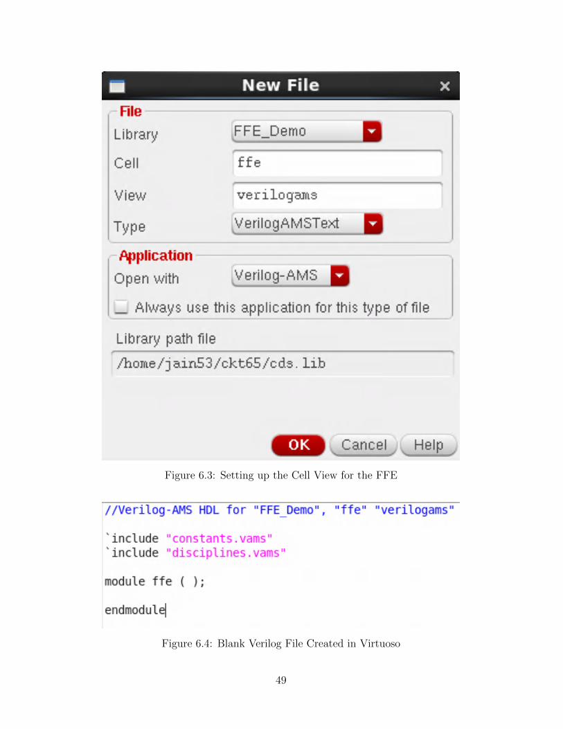
Figure 6.3: Setting up the Cell View for the FFE
Figure 6.4: Blank Verilog File Created in Virtuoso
49
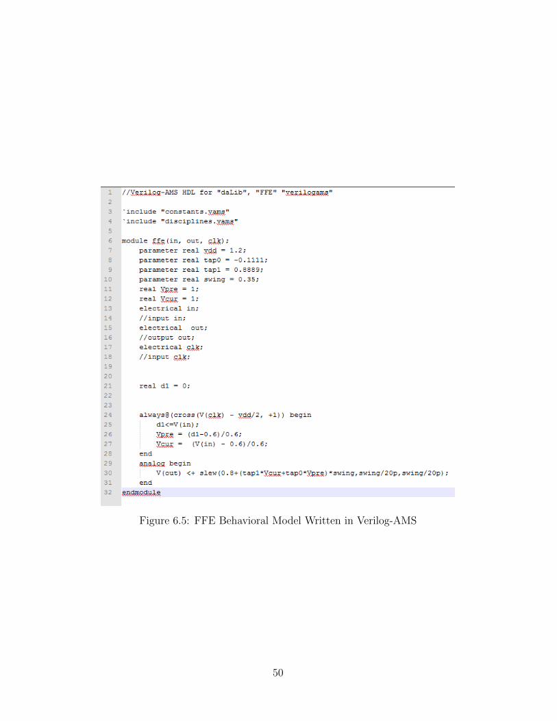
Figure 6.5: FFE Behavioral Model Written in Verilog-AMS
50
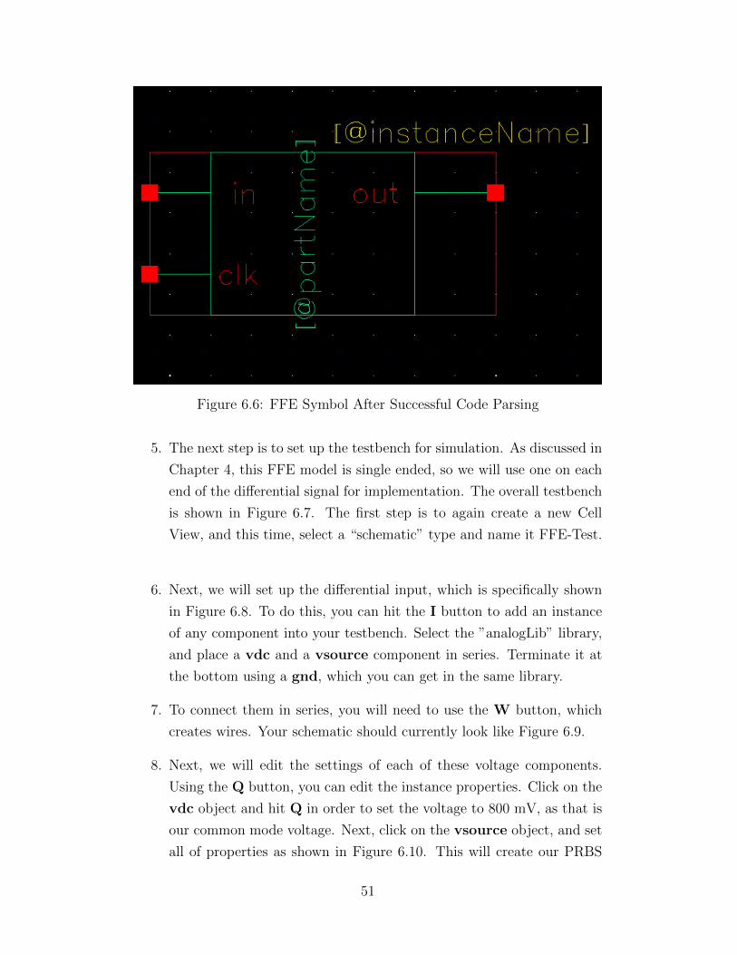
Figure 6.6: FFE Symbol After Successful Code Parsing
5. The next step is to set up the testbench for simulation. As discussed in
Chapter 4, this FFE model is single ended, so we will use one on each
end of the differential signal for implementation. The overall testbench
is shown in Figure 6.7. The first step is to again create a new Cell
View, and this time, select a “schematic” type and name it FFE-Test.
6. Next, we will set up the differential input, which is specifically shown
in Figure 6.8. To do this, you can hit the I button to add an instance
of any component into your testbench. Select the ”analogLib” library,
and place a vdc and a vsource component in series. Terminate it at
the bottom using a gnd, which you can get in the same library.
7. To connect them in series, you will need to use the W button, which
creates wires. Your schematic should currently look like Figure 6.9.
8. Next, we will edit the settings of each of these voltage components.
Using the Q button, you can edit the instance properties. Click on the
vdc object and hit Q in order to set the voltage to 800 mV, as that is
our common mode voltage. Next, click on the vsource object, and set
all of properties as shown in Figure 6.10. This will create our PRBS
51
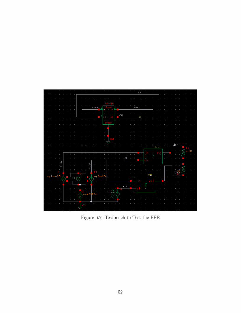
Figure 6.7: Testbench to Test the FFE
52
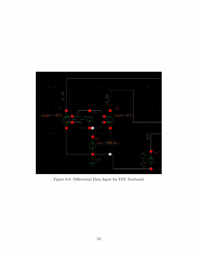
Figure 6.8: Differential Data Input for FFE Testbench
53
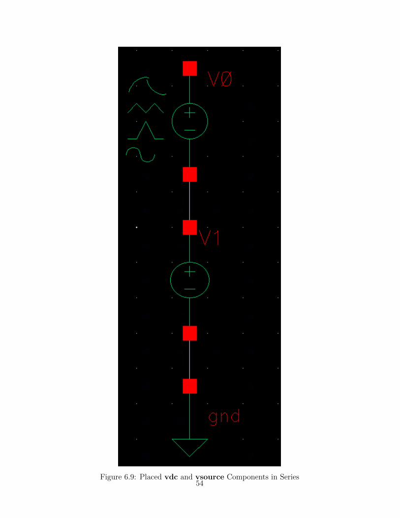
Figure 6.9: Placed vdc and vsource Components in Series54
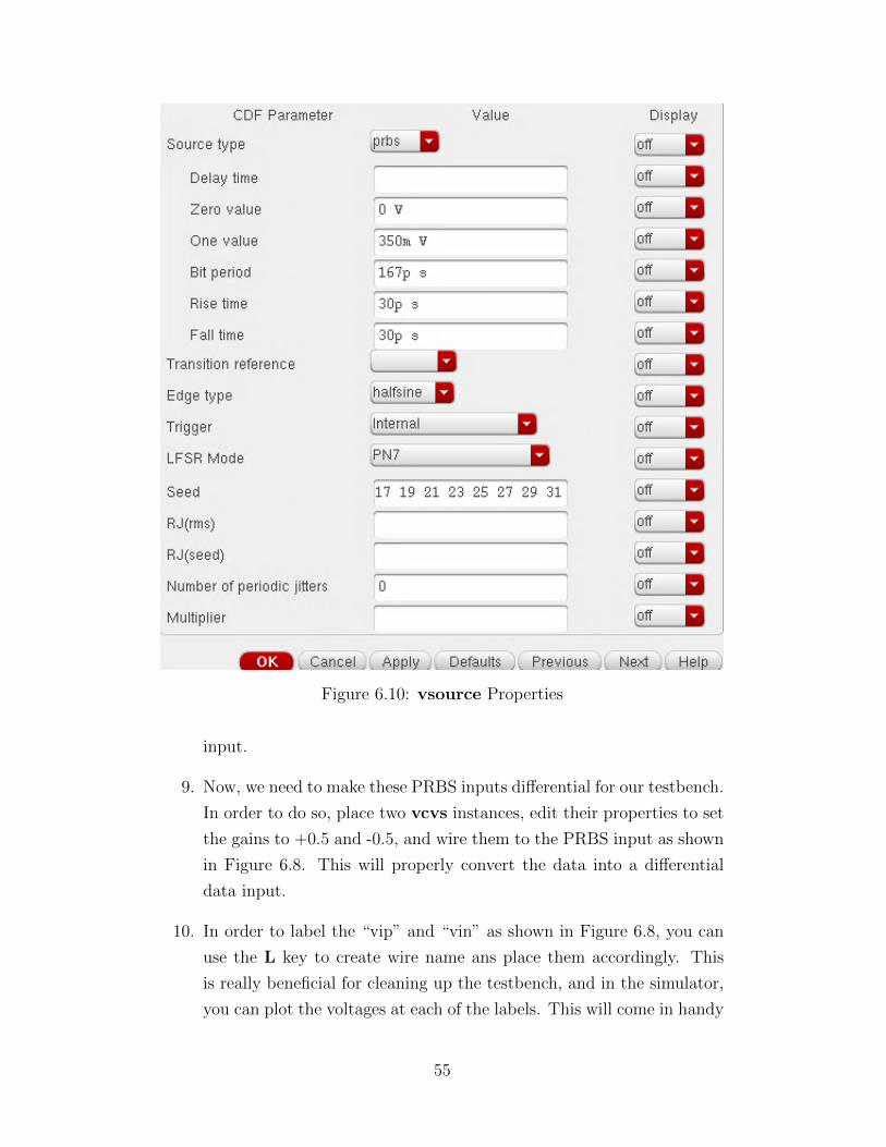
Figure 6.10: vsource Properties
input.
9. Now, we need to make these PRBS inputs differential for our testbench.
In order to do so, place two vcvs instances, edit their properties to set
the gains to +0.5 and -0.5, and wire them to the PRBS input as shown
in Figure 6.8. This will properly convert the data into a differential
data input.
10. In order to label the “vip” and “vin” as shown in Figure 6.8, you can
use the L key to create wire name ans place them accordingly. This
is really beneficial for cleaning up the testbench, and in the simulator,
you can plot the voltages at each of the labels. This will come in handy
55
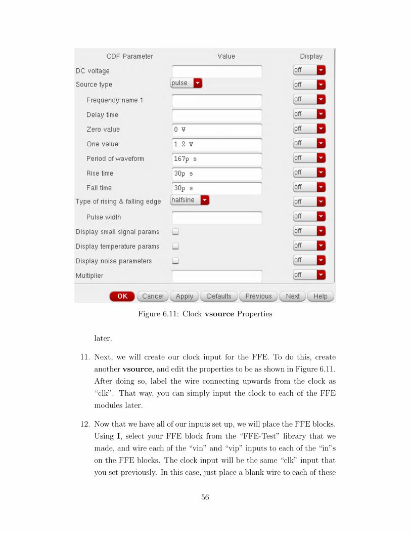
Figure 6.11: Clock vsource Properties
later.
11. Next, we will create our clock input for the FFE. To do this, create
another vsource, and edit the properties to be as shown in Figure 6.11.
After doing so, label the wire connecting upwards from the clock as
“clk”. That way, you can simply input the clock to each of the FFE
modules later.
12. Now that we have all of our inputs set up, we will place the FFE blocks.
Using I, select your FFE block from the “FFE-Test” library that we
made, and wire each of the “vin” and “vip” inputs to each of the “in”s
on the FFE blocks. The clock input will be the same “clk” input that
you set previously. In this case, just place a blank wire to each of these
56
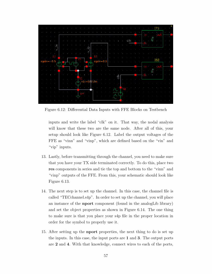
Figure 6.12: Differential Data Inputs with FFE Blocks on Testbench
inputs and write the label “clk” on it. That way, the nodal analysis
will know that these two are the same node. After all of this, your
setup should look like Figure 6.12. Label the output voltages of the
FFE as “vinn” and “vinp”, which are defined based on the “vin” and
“vip” inputs.
13. Lastly, before transmitting through the channel, you need to make sure
that you have your TX side terminated correctly. To do this, place two
res components in series and tie the top and bottom to the “vinn” and
“vinp” outputs of the FFE. From this, your schematic should look like
Figure 6.13.
14. The next step is to set up the channel. In this case, the channel file is
called “TECchannel.s4p”. In order to set up the channel, you will place
an instance of the nport component (found in the analogLib library)
and set the object properties as shown in Figure 6.14. The one thing
to make sure is that you place your s4p file in the proper location in
order for the symbol to properly use it.
15. After setting up the nport properties, the next thing to do is set up
the inputs. In this case, the input ports are 1 and 3. The output ports
are 2 and 4. With that knowledge, connect wires to each of the ports,
57
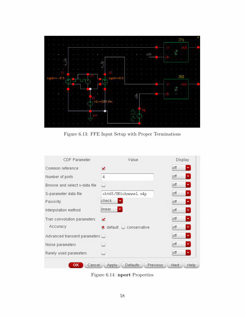
Figure 6.13: FFE Input Setup with Proper Terminations
Figure 6.14: nport Properties
58
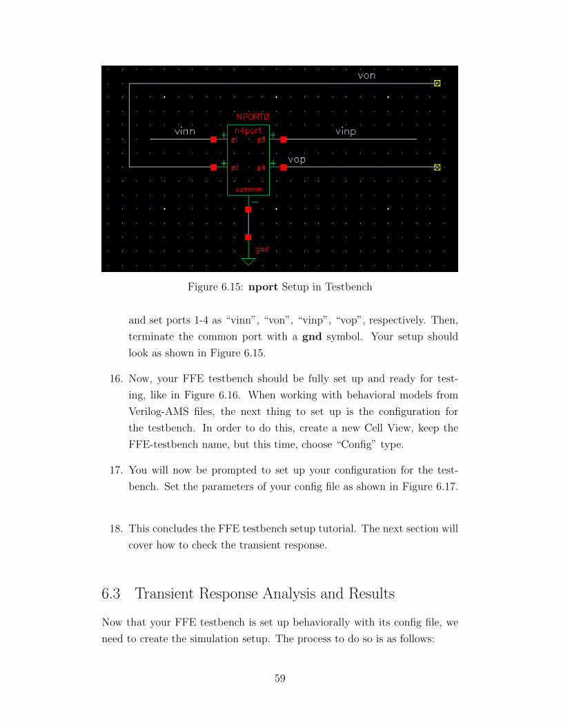
Figure 6.15: nport Setup in Testbench
and set ports 1-4 as “vinn”, “von”, “vinp”, “vop”, respectively. Then,
terminate the common port with a gnd symbol. Your setup should
look as shown in Figure 6.15.
16. Now, your FFE testbench should be fully set up and ready for test-
ing, like in Figure 6.16. When working with behavioral models from
Verilog-AMS files, the next thing to set up is the configuration for
the testbench. In order to do this, create a new Cell View, keep the
FFE-testbench name, but this time, choose “Config” type.
17. You will now be prompted to set up your configuration for the test-
bench. Set the parameters of your config file as shown in Figure 6.17.
18. This concludes the FFE testbench setup tutorial. The next section will
cover how to check the transient response.
6.3 Transient Response Analysis and Results
Now that your FFE testbench is set up behaviorally with its config file, we
need to create the simulation setup. The process to do so is as follows:
59
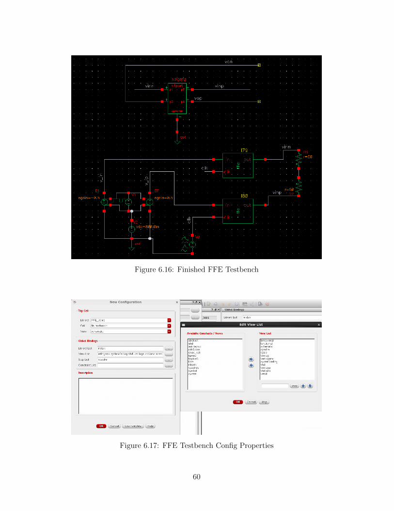
Figure 6.16: Finished FFE Testbench
Figure 6.17: FFE Testbench Config Properties
60
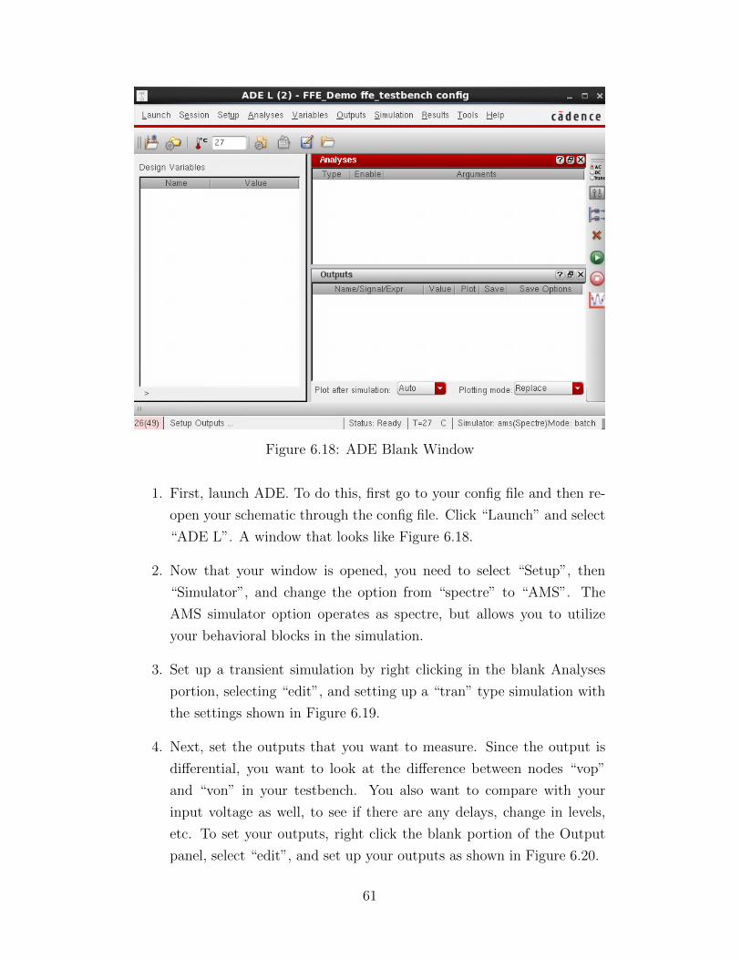
Figure 6.18: ADE Blank Window
1. First, launch ADE. To do this, first go to your config file and then re-
open your schematic through the config file. Click “Launch” and select
“ADE L”. A window that looks like Figure 6.18.
2. Now that your window is opened, you need to select “Setup”, then
“Simulator”, and change the option from “spectre” to “AMS”. The
AMS simulator option operates as spectre, but allows you to utilize
your behavioral blocks in the simulation.
3. Set up a transient simulation by right clicking in the blank Analyses
portion, selecting “edit”, and setting up a “tran” type simulation with
the settings shown in Figure 6.19.
4. Next, set the outputs that you want to measure. Since the output is
differential, you want to look at the difference between nodes “vop”
and “von” in your testbench. You also want to compare with your
input voltage as well, to see if there are any delays, change in levels,
etc. To set your outputs, right click the blank portion of the Output
panel, select “edit”, and set up your outputs as shown in Figure 6.20.
61
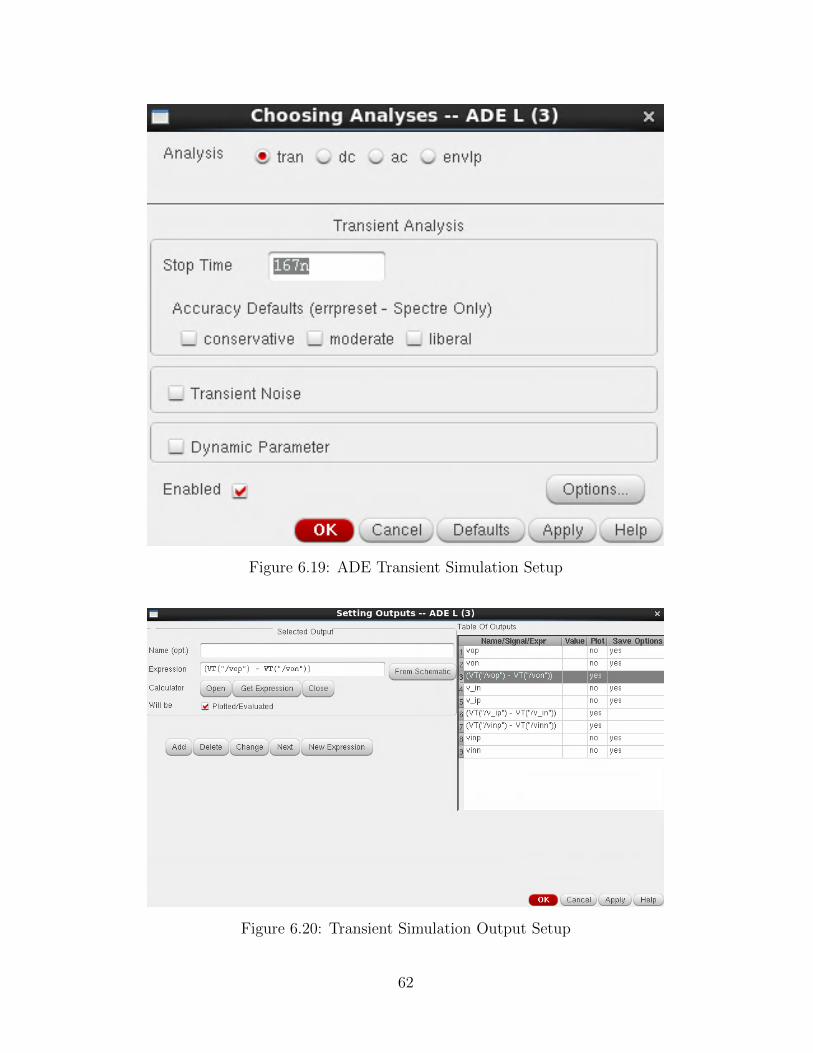
Figure 6.19: ADE Transient Simulation Setup
Figure 6.20: Transient Simulation Output Setup
62
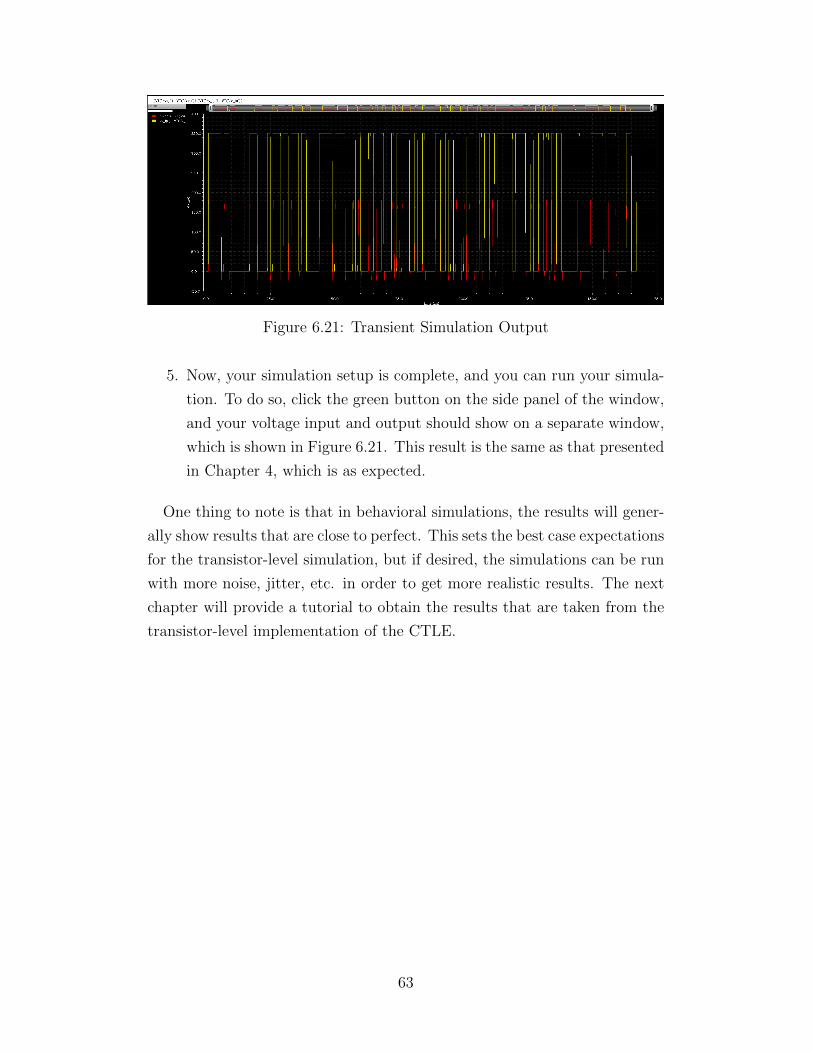
Figure 6.21: Transient Simulation Output
5. Now, your simulation setup is complete, and you can run your simula-
tion. To do so, click the green button on the side panel of the window,
and your voltage input and output should show on a separate window,
which is shown in Figure 6.21. This result is the same as that presented
in Chapter 4, which is as expected.
One thing to note is that in behavioral simulations, the results will gener-
ally show results that are close to perfect. This sets the best case expectations
for the transistor-level simulation, but if desired, the simulations can be run
with more noise, jitter, etc. in order to get more realistic results. The next
chapter will provide a tutorial to obtain the results that are taken from the
transistor-level implementation of the CTLE.
63
CHAPTER 7
TRANSISTOR LEVEL SIMULATION OFCTLE
7.1 Overview of Simulation
SPICE is a circuit simulator that numerically solves the circuits through
nodal analysis. Because of this, it is capable of performing a DC, transient,
and AC analysis (along with a few other types) for electronic circuits con-
taining resistors, capacitors, inductors, transmission lines (both lossy and
lossless), switches, ideal voltage/current sources, dependent voltage/current
sources, etc. Most importantly, it can simulate MOSFETs, which is critical
for testing the CTLE in this section. Cadence Spectre is a variant of SPICE
that is used to perform these simulations. Unlike SPICE, Spectre simulates
analog and digital circuits at a differential equation level. However, both use
nodal analysis to calculate the solutions to the matrices. Overall, Spectre is
a better tool, as it is optimized for both speed and accuracy.
7.2 CTLE Design Setup
In Chapter 5, we presented the schematic for the CTLE (as shown in Fig-
ure 5.2). To recap, here is the list of component values for our CTLE:
1. W = 12.5 µm
2. L = 100 nm
3. Ibias = 250 µA
4. CD = 1.52 pF
5. RD = 209 Ω
6. RL = 1.2 kΩ
64
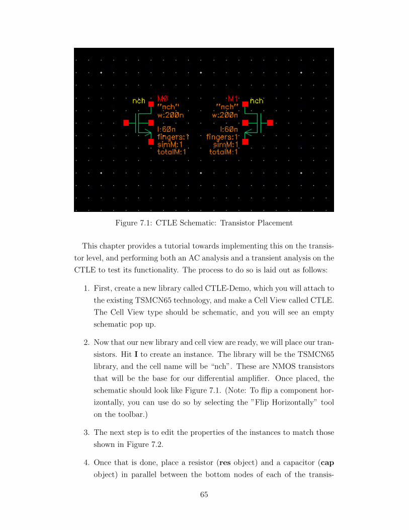
Figure 7.1: CTLE Schematic: Transistor Placement
This chapter provides a tutorial towards implementing this on the transis-
tor level, and performing both an AC analysis and a transient analysis on the
CTLE to test its functionality. The process to do so is laid out as follows:
1. First, create a new library called CTLE-Demo, which you will attach to
the existing TSMCN65 technology, and make a Cell View called CTLE.
The Cell View type should be schematic, and you will see an empty
schematic pop up.
2. Now that our new library and cell view are ready, we will place our tran-
sistors. Hit I to create an instance. The library will be the TSMCN65
library, and the cell name will be “nch”. These are NMOS transistors
that will be the base for our differential amplifier. Once placed, the
schematic should look like Figure 7.1. (Note: To flip a component hor-
izontally, you can use do so by selecting the ”Flip Horizontally” tool
on the toolbar.)
3. The next step is to edit the properties of the instances to match those
shown in Figure 7.2.
4. Once that is done, place a resistor (res object) and a capacitor (cap
object) in parallel between the bottom nodes of each of the transis-
65
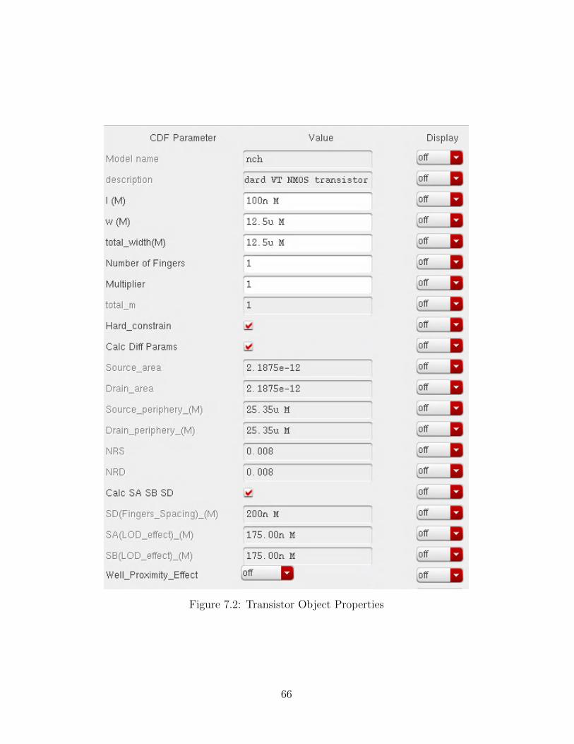
Figure 7.2: Transistor Object Properties
66
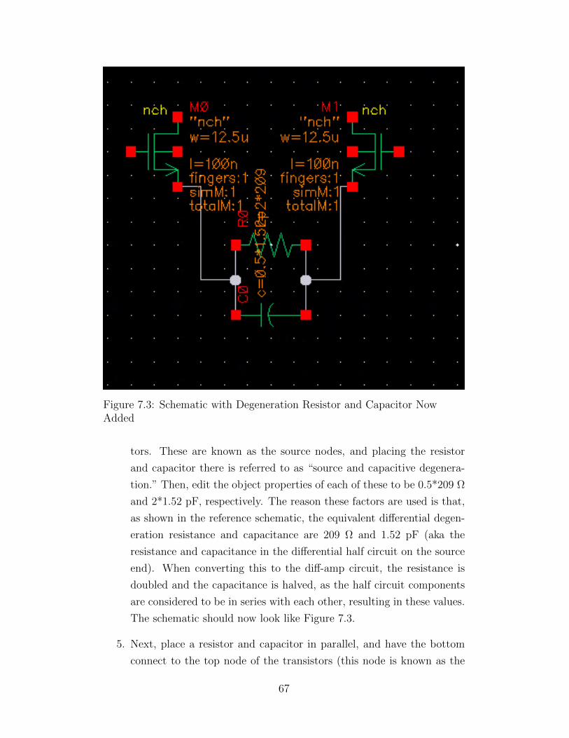
Figure 7.3: Schematic with Degeneration Resistor and Capacitor NowAdded
tors. These are known as the source nodes, and placing the resistor
and capacitor there is referred to as “source and capacitive degenera-
tion.” Then, edit the object properties of each of these to be 0.5*209 Ω
and 2*1.52 pF, respectively. The reason these factors are used is that,
as shown in the reference schematic, the equivalent differential degen-
eration resistance and capacitance are 209 Ω and 1.52 pF (aka the
resistance and capacitance in the differential half circuit on the source
end). When converting this to the diff-amp circuit, the resistance is
doubled and the capacitance is halved, as the half circuit components
are considered to be in series with each other, resulting in these values.
The schematic should now look like Figure 7.3.
5. Next, place a resistor and capacitor in parallel, and have the bottom
connect to the top node of the transistors (this node is known as the
67
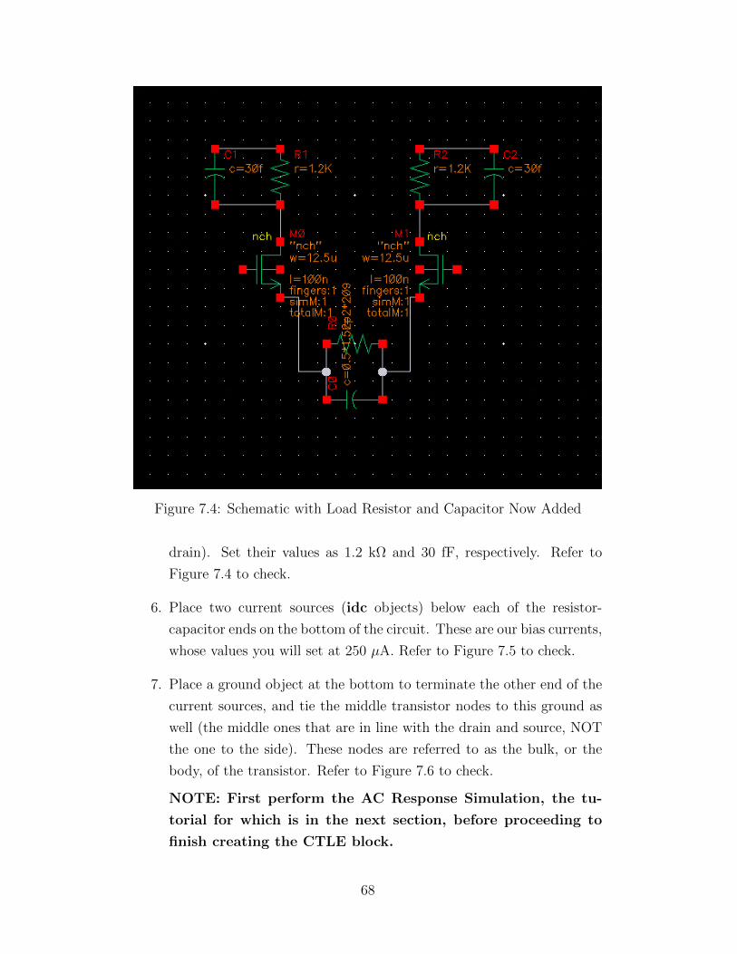
Figure 7.4: Schematic with Load Resistor and Capacitor Now Added
drain). Set their values as 1.2 kΩ and 30 fF, respectively. Refer to
Figure 7.4 to check.
6. Place two current sources (idc objects) below each of the resistor-
capacitor ends on the bottom of the circuit. These are our bias currents,
whose values you will set at 250 µA. Refer to Figure 7.5 to check.
7. Place a ground object at the bottom to terminate the other end of the
current sources, and tie the middle transistor nodes to this ground as
well (the middle ones that are in line with the drain and source, NOT
the one to the side). These nodes are referred to as the bulk, or the
body, of the transistor. Refer to Figure 7.6 to check.
NOTE: First perform the AC Response Simulation, the tu-
torial for which is in the next section, before proceeding to
finish creating the CTLE block.
68
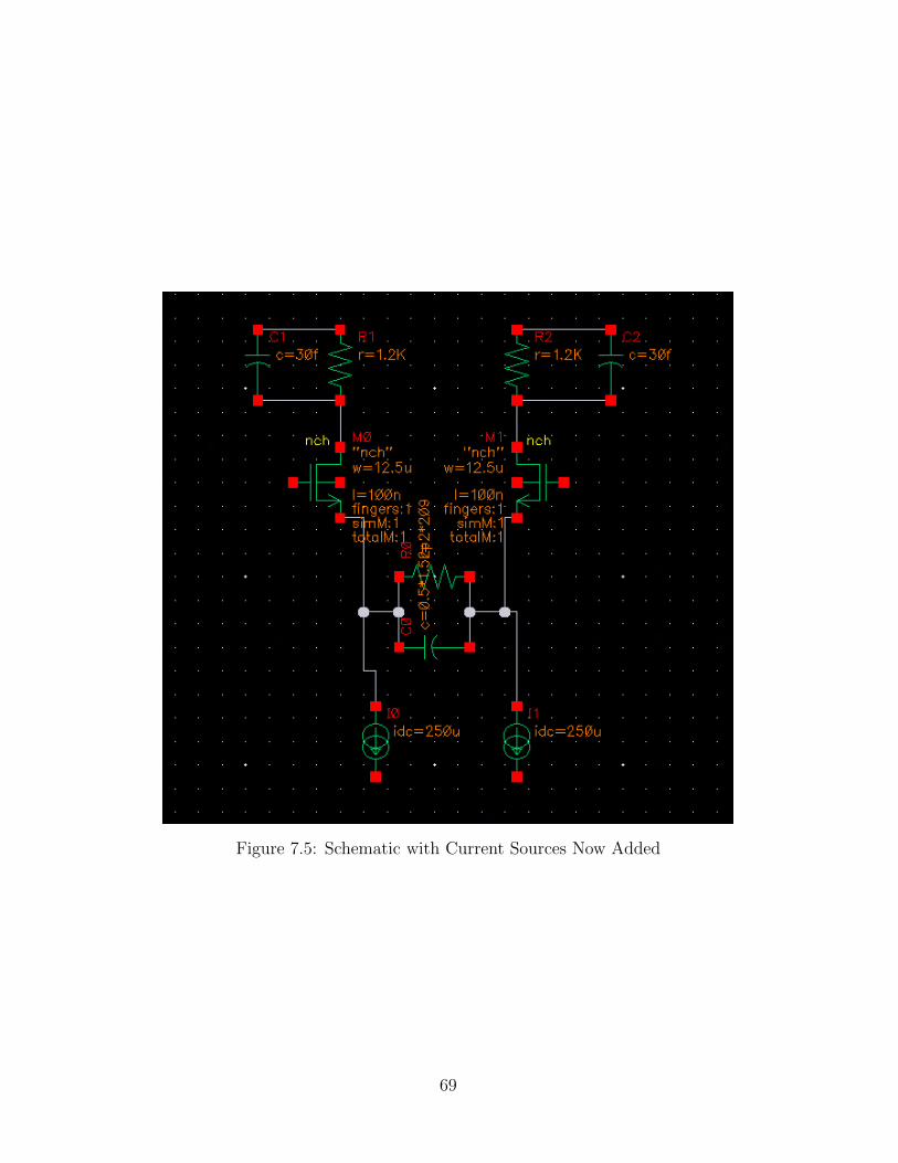
Figure 7.5: Schematic with Current Sources Now Added
69
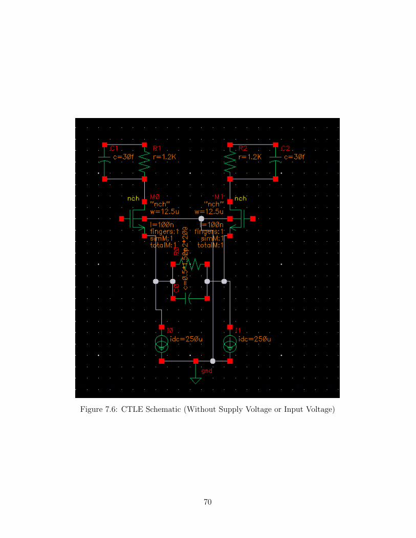
Figure 7.6: CTLE Schematic (Without Supply Voltage or Input Voltage)
70

8. After verifying the AC performance of the CTLE, it is time to revert
the design back to that shown in Figure 7.6. Basically, delete the wire
labels and the input setup.
9. Now, use the P button to place pins. These pins can either be input,
output, or inputoutput. In this setup, we use four input pins and two
output pins. Create two input pins, labeled “vin” and “vip”, that will
connect to the left and right transistor gates, respectively.
10. Next, place one input pin connected to the top wire of the load resistor-
capacitors labelled as “vdd.”
11. Place one input pin connected to the bottom of the current sources,
labeled “gnd”.
12. Place two output pins, labeled “voutn” and “voutp”, connected to the
drains of the left and right transistor, respectively. Your schematic
should now look like Figure 7.7.
13. Finally, it is time to create the symbol. Select “Create”, then “Cel-
lview”, then “From Cellview”, and click ok. The default option is to
create a symbol, and in this case, that is what we need.
14. For convenience, set the top pin to “vdd”, the bottom pin to “gnd”,
the left pins to “vin” and “vip”, and lastly, the right pins to “voutn”
and “voutp”. Refer to Figure 7.8. Rearrange the pins, if desired. Now,
the CTLE transistor-level block has been completed.
7.3 AC Response Analysis and Results
At this point, your CTLE schematic should be complete (Step 7). Now,
the objective is to validate your component selection by checking the AC
response. This response verifies that your peaking range, your peaking gain,
and your DC gain are appropriate.
1. First, draw wires out of the drain of each of the transistors. Label them
“voutn” and “voutp”, respectively.
71
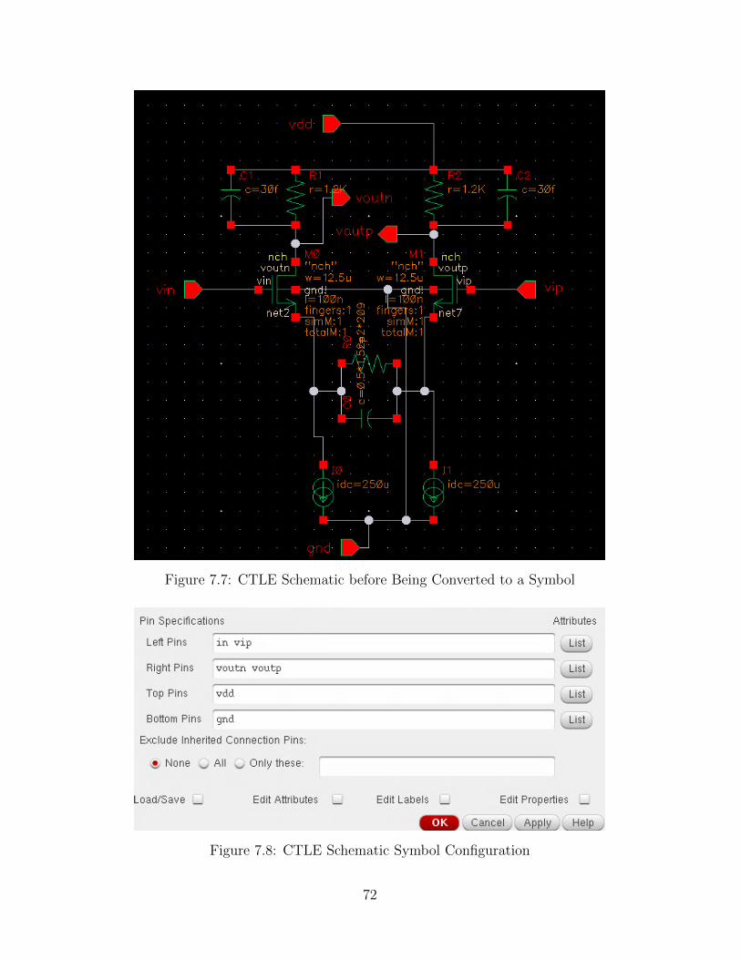
Figure 7.7: CTLE Schematic before Being Converted to a Symbol
Figure 7.8: CTLE Schematic Symbol Configuration
72
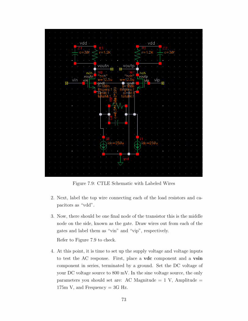
Figure 7.9: CTLE Schematic with Labeled Wires
2. Next, label the top wire connecting each of the load resistors and ca-
pacitors as “vdd”.
3. Now, there should be one final node of the transistor this is the middle
node on the side, known as the gate. Draw wires out from each of the
gates and label them as “vin” and “vip”, respectively.
Refer to Figure 7.9 to check.
4. At this point, it is time to set up the supply voltage and voltage inputs
to test the AC response. First, place a vdc component and a vsin
component in series, terminated by a ground. Set the DC voltage of
your DC voltage source to 800 mV. In the sine voltage source, the only
parameters you should set are: AC Magnitude = 1 V, Amplitude =
175m V, and Frequency = 3G Hz.
73
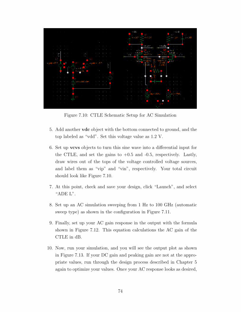
Figure 7.10: CTLE Schematic Setup for AC Simulation
5. Add another vdc object with the bottom connected to ground, and the
top labeled as “vdd”. Set this voltage value as 1.2 V.
6. Set up vcvs objects to turn this sine wave into a differential input for
the CTLE, and set the gains to +0.5 and -0.5, respectively. Lastly,
draw wires out of the tops of the voltage controlled voltage sources,
and label them as “vip” and “vin”, respectively. Your total circuit
should look like Figure 7.10.
7. At this point, check and save your design, click “Launch”, and select
“ADE L”.
8. Set up an AC simulation sweeping from 1 Hz to 100 GHz (automatic
sweep type) as shown in the configuration in Figure 7.11.
9. Finally, set up your AC gain response in the output with the formula
shown in Figure 7.12. This equation calculations the AC gain of the
CTLE in dB.
10. Now, run your simulation, and you will see the output plot as shown
in Figure 7.13. If your DC gain and peaking gain are not at the appro-
priate values, run through the design process described in Chapter 5
again to optimize your values. Once your AC response looks as desired,
74
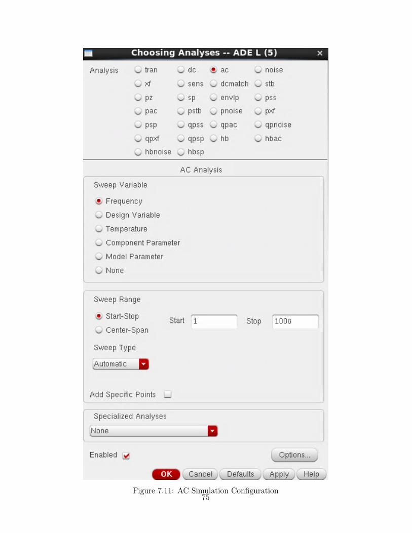
Figure 7.11: AC Simulation Configuration75
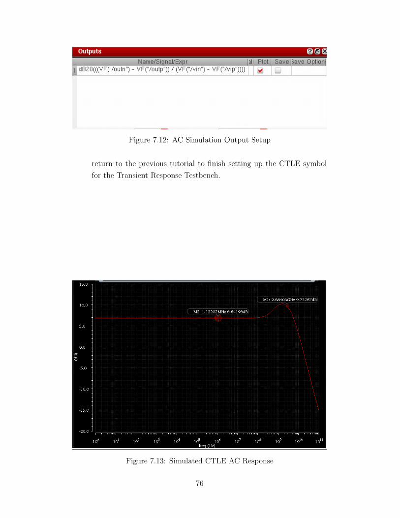
Figure 7.12: AC Simulation Output Setup
return to the previous tutorial to finish setting up the CTLE symbol
for the Transient Response Testbench.
Figure 7.13: Simulated CTLE AC Response
76
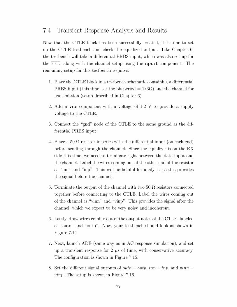
7.4 Transient Response Analysis and Results
Now that the CTLE block has been successfully created, it is time to set
up the CTLE testbench and check the equalized output. Like Chapter 6,
the testbench will take a differential PRBS input, which was also set up for
the FFE, along with the channel setup using the nport component. The
remaining setup for this testbench requires:
1. Place the CTLE block in a testbench schematic containing a differential
PRBS input (this time, set the bit period = 1/3G) and the channel for
transmission (setup described in Chapter 6)
2. Add a vdc component with a voltage of 1.2 V to provide a supply
voltage to the CTLE.
3. Connect the “gnd” node of the CTLE to the same ground as the dif-
ferential PRBS input.
4. Place a 50 Ω resistor in series with the differential input (on each end)
before sending through the channel. Since the equalizer is on the RX
side this time, we need to terminate right between the data input and
the channel. Label the wires coming out of the other end of the resistor
as “inn” and “inp”. This will be helpful for analysis, as this provides
the signal before the channel.
5. Terminate the output of the channel with two 50 Ω resistors connected
together before connecting to the CTLE. Label the wires coming out
of the channel as “vinn” and “vinp”. This provides the signal after the
channel, which we expect to be very noisy and incoherent.
6. Lastly, draw wires coming out of the output notes of the CTLE, labeled
as “outn” and “outp”. Now, your testbench should look as shown in
Figure 7.14
7. Next, launch ADE (same way as in AC response simulation), and set
up a transient response for 2 µs of time, with conservative accuracy.
The configuration is shown in Figure 7.15.
8. Set the different signal outputs of outn− outp, inn− inp, and vinn−vinp. The setup is shown in Figure 7.16.
77
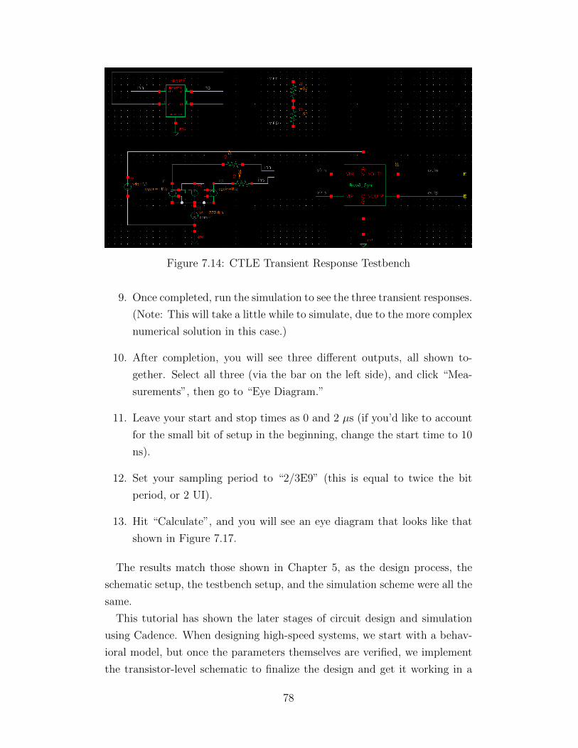
Figure 7.14: CTLE Transient Response Testbench
9. Once completed, run the simulation to see the three transient responses.
(Note: This will take a little while to simulate, due to the more complex
numerical solution in this case.)
10. After completion, you will see three different outputs, all shown to-
gether. Select all three (via the bar on the left side), and click “Mea-
surements”, then go to “Eye Diagram.”
11. Leave your start and stop times as 0 and 2 µs (if you’d like to account
for the small bit of setup in the beginning, change the start time to 10
ns).
12. Set your sampling period to “2/3E9” (this is equal to twice the bit
period, or 2 UI).
13. Hit “Calculate”, and you will see an eye diagram that looks like that
shown in Figure 7.17.
The results match those shown in Chapter 5, as the design process, the
schematic setup, the testbench setup, and the simulation scheme were all the
same.
This tutorial has shown the later stages of circuit design and simulation
using Cadence. When designing high-speed systems, we start with a behav-
ioral model, but once the parameters themselves are verified, we implement
the transistor-level schematic to finalize the design and get it working in a
78
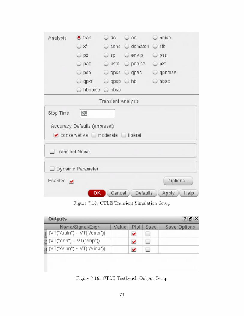
Figure 7.15: CTLE Transient Simulation Setup
Figure 7.16: CTLE Testbench Output Setup
79
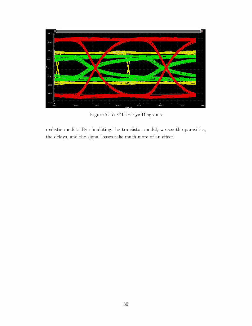
Figure 7.17: CTLE Eye Diagrams
realistic model. By simulating the transistor model, we see the parasitics,
the delays, and the signal losses take much more of an effect.
80
CHAPTER 8
DISCUSSION
8.1 Comparison of Results
In this thesis, equalization at both the transmitting (TX) and receiving (RX)
ends of a serial link is analyzed. In both cases, the design process is discussed,
both mathematically and electrically. In the first case, we look at equaliza-
tion in discrete time, where we only care about the sampled responses of
the link. Using that knowledge, we discuss how to determine the optimal
mathematical coefficients that are needed to design a feed-forward equalizer
(FFE) on the transmitting side. These coefficients are used in implementing
a pre-emphasis filter. In the second case, we look at equalization in con-
tinuous time, where we care about the voltage at every point in time, as
we want to accomplish faster transition times and higher voltage levels with
our equalizer. We then determine the specifications for our system in order
to calculate the component values of our continuous-time linear equalizer’s
(CTLE) circuit topology. The objective that is common in both cases is
to counteract the transfer function of the channel, whether in discrete time
(z-domain) or in continuous time (s-domain).
The results in Chapter 4 showed a working behavioral model of the FFE
that successfully accounted for a lot of the ISI in the channel, but still caused
an unwanted voltage output, due to only eliminating the precursors. There
were different voltage levels, which is better represented in Figure 8.1.
In this figure, the different voltage levels run during one bit period, which
will increase the BER. Furthermore, in circuit-level implementation, sam-
pling the signal means that clock jitter can affect the equalization output,
along with potential synchronization issues. Lastly, because of the multiple
taps (multiple amplifiers in our proposed topology), the FFE will also con-
sume more power, whereas the CTLE topology uses one differential amplifier.
81
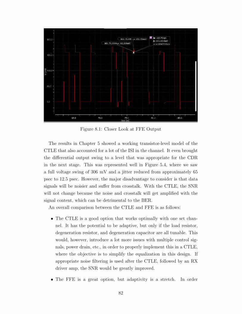
Figure 8.1: Closer Look at FFE Output
The results in Chapter 5 showed a working transistor-level model of the
CTLE that also accounted for a lot of the ISI in the channel. It even brought
the differential output swing to a level that was appropriate for the CDR
in the next stage. This was represented well in Figure 5.4, where we saw
a full voltage swing of 306 mV and a jitter reduced from approximately 65
psec to 12.5 psec. However, the major disadvantage to consider is that data
signals will be noisier and suffer from crosstalk. With the CTLE, the SNR
will not change because the noise and crosstalk will get amplified with the
signal content, which can be detrimental to the BER.
An overall comparison between the CTLE and FFE is as follows:
• The CTLE is a good option that works optimally with one set chan-
nel. It has the potential to be adaptive, but only if the load resistor,
degeneration resistor, and degeneration capacitor are all tunable. This
would, however, introduce a lot more issues with multiple control sig-
nals, power drain, etc., in order to properly implement this in a CTLE,
where the objective is to simplify the equalization in this design. If
appropriate noise filtering is used after the CTLE, followed by an RX
driver amp, the SNR would be greatly improved.
• The FFE is a great option, but adaptivity is a stretch. In order
82
to accomplish adaptivity, the matrix solution for the coefficients will
need to be generated based on the channel’s performance, which is
too complex to implement, test, and optimize within the scope of an
HSSL. Furthermore, there is still ISI after implementation, along with
the noise/crosstalk remaining untouched. With appropriate filtering,
enough taps on the FFE (based on the channel’s pulse response), and
close to perfect sampling from the PLL’s clock, the FFE would be a
good solution.
8.2 Future Work
At higher speeds (and in turn, higher loss/parasitics), it is clear that both the
FFE and CTLE start to fall in their maximum potential. However, a more
complex equalization solution can be made, also utilizing a decision-feedback
equalizer (DFE). The DFE is a non-linear RX equalizer that utilizes a slicer
in order to decide if the symbol is “1” or “0”. After making a decision, the
DFE utilizes an RX FIR filter in feedback to subtract the ISI directly. Since
the coefficients are directly taken from the channel response, this equalizer
can be made to be adaptable. Furthermore, this equalizer improves SNR
since it solely improves the signal without amplifying noise and crosstalk as
well.
However, there are also some issues that exist with this implementation.
Firstly, since the DFE utilizes an RX FIR filter, it only accounts for the
postcursors, so an FFE would still be beneficial to eliminate the precursor
(our implementation would work very well here). Furthermore, if the decision
circuit is incorrect, the error will propagate to later bits, causing higher BER.
Lastly, since the DFE will need an accurate clock, which will most likely come
from the CDR, the clock jitter can play a very detrimental effect on the DFE’s
performance.
For future work, this design process can be utilized to implement an equal-
ization system utilizing an FFE, a CTLE, and a DFE. The representation of
this system is shown in Figure 8.2 [17]. The implementation of this system
would be done by following this design process:
1. Design a CTLE to account for enough loss at the operating frequency
in order to improve the ISI.
83
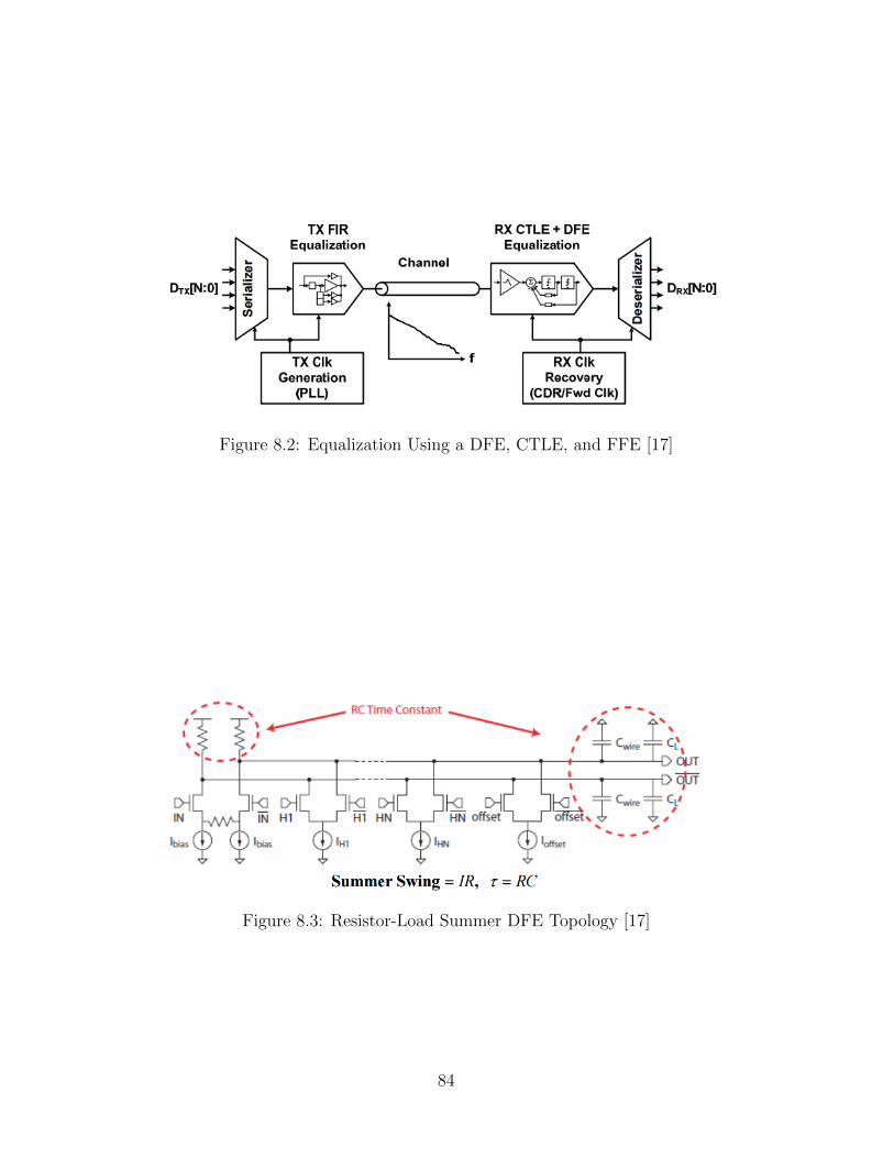
Figure 8.2: Equalization Using a DFE, CTLE, and FFE [17]
Figure 8.3: Resistor-Load Summer DFE Topology [17]
84
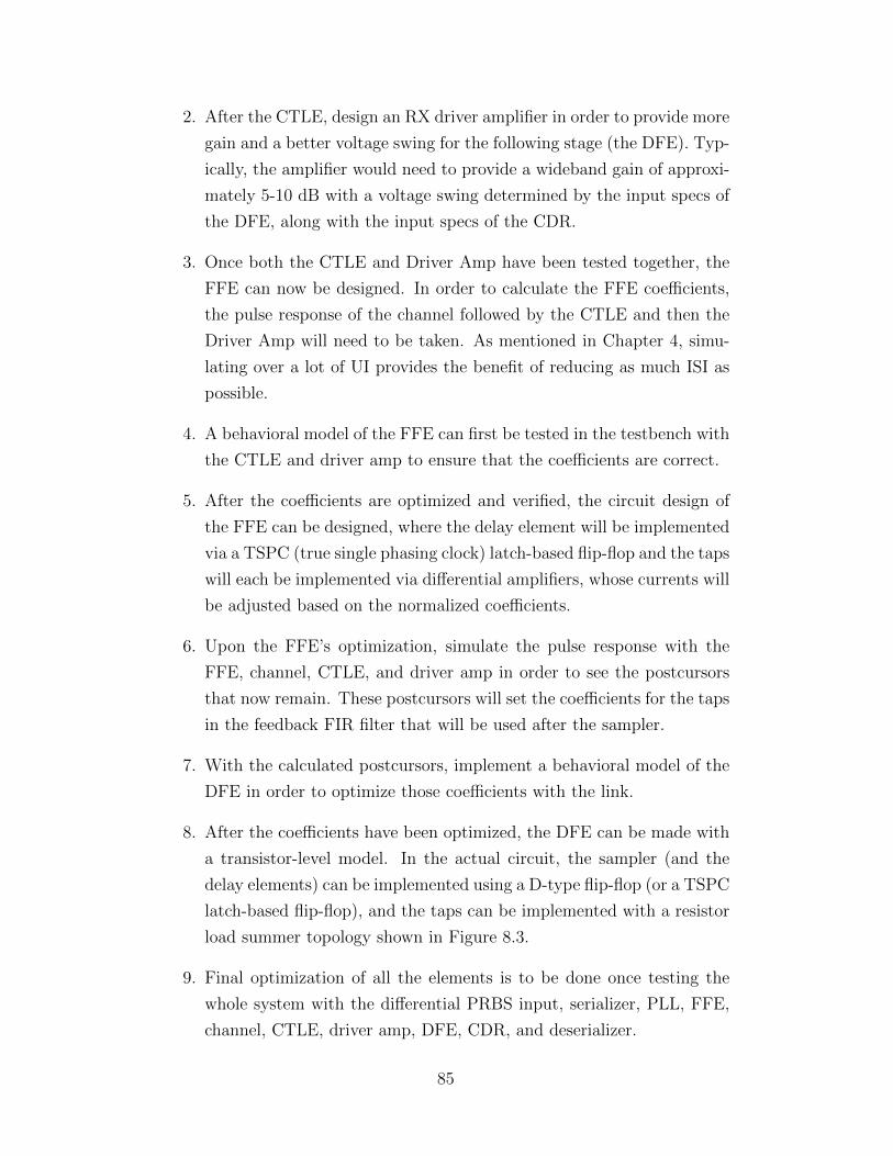
2. After the CTLE, design an RX driver amplifier in order to provide more
gain and a better voltage swing for the following stage (the DFE). Typ-
ically, the amplifier would need to provide a wideband gain of approxi-
mately 5-10 dB with a voltage swing determined by the input specs of
the DFE, along with the input specs of the CDR.
3. Once both the CTLE and Driver Amp have been tested together, the
FFE can now be designed. In order to calculate the FFE coefficients,
the pulse response of the channel followed by the CTLE and then the
Driver Amp will need to be taken. As mentioned in Chapter 4, simu-
lating over a lot of UI provides the benefit of reducing as much ISI as
possible.
4. A behavioral model of the FFE can first be tested in the testbench with
the CTLE and driver amp to ensure that the coefficients are correct.
5. After the coefficients are optimized and verified, the circuit design of
the FFE can be designed, where the delay element will be implemented
via a TSPC (true single phasing clock) latch-based flip-flop and the taps
will each be implemented via differential amplifiers, whose currents will
be adjusted based on the normalized coefficients.
6. Upon the FFE’s optimization, simulate the pulse response with the
FFE, channel, CTLE, and driver amp in order to see the postcursors
that now remain. These postcursors will set the coefficients for the taps
in the feedback FIR filter that will be used after the sampler.
7. With the calculated postcursors, implement a behavioral model of the
DFE in order to optimize those coefficients with the link.
8. After the coefficients have been optimized, the DFE can be made with
a transistor-level model. In the actual circuit, the sampler (and the
delay elements) can be implemented using a D-type flip-flop (or a TSPC
latch-based flip-flop), and the taps can be implemented with a resistor
load summer topology shown in Figure 8.3.
9. Final optimization of all the elements is to be done once testing the
whole system with the differential PRBS input, serializer, PLL, FFE,
channel, CTLE, driver amp, DFE, CDR, and deserializer.
85

As discussed in the beginning, the major assumption made in this design
process is that the serializer, PLL, CDR, and deserializer work without any
detrimental contributions to the equalizer’s performance. When incorporat-
ing the realistic effects of each of these modules, this process becomes more
iterative within each step, as optimizing each module requires proper timing,
parasitic, noise, and jitter analysis in order to ensure successful equalization.
86
REFERENCES
[1] IDC, “IDC Predictions 2013: Competing on the 3rd Platform,” Nov.2012. [Online]. Available: http://www.idc.com/research/Predictions13/downloadable/238044.pdf
[2] D. Friedman, “International Solid-State Circuits Conference Trends2013,” Feb. 2013. [Online]. Available: http://isscc.org/doc/2013/2013Trends.pdf
[3] R. Vetter, D. Du, and A. Klietz, “Network Supercomputing,” IEEENetwork, vol. 6, no. 3, pp. 38–44, May 1992.
[4] B. Razavi, Monolithic Phase-Locked Loops and Clocked Recovery Cir-cuits. IEEE Press, 1996.
[5] J. C. Chen, “Multi-Gigabit SERDES: The Corner-Stone of High Speed Serial Interconnects,” 2011. [On-line]. Available: http://www.design-reuse.com/articles/10541/multi-gigabitserdes-the-cornerstone-of-high-speed-serial-interconnects.html
[6] R. Farjadrad, “What’s the difference between optical and electrical
technology for 100-gbit/s connectivity in future systems?” July 2014.[Online]. Available: http://electronicdesign.com/communications/what-s-difference-between-optical-and-electrical-technology-100-gbits-connectivity-fu
[7] E. Alon, “High-Speed Electrical Interface Circuit Design: Lecture1,” 2014. [Online]. Available: http://bwrcs.eecs.berkeley.edu/Classes/icdesign/ee290cs11/lectures/Lecture01Intro 2up.pdf
[8] V. Stojanovic, “Channel-Limited High-Speed Links: Modeling,
Analysis, and Design,” Ph.D. dissertation, Stanford University, PaloAlto, 2004. [Online]. Available: http://chipgen.stanford.edu/papers/vsthesis.pdf
87
[9] P. K. Hanumolu, “Design techniques for clocking highperformance signaling systems,” Ph.D. dissertation, Ore-gon State University, Corvallis, 2006. [Online]. Avail-able: http://ir.library.oregonstate.edu/xmlui/bitstream/handle/1957/3530/20061016+pavan+dissertation.pdf?sequence=1
[10] S. Palermo, CMOS Nanoelectronics Analog and RF VLSI Circuits. NewYork City, NY: McGraw-Hill, 2011.
[11] “AND9075/D application note: Understanding data eye di-agram methodology for analyzing high speed digital sig-nals,” ON Semiconductor, June 2015. [Online]. Available:http://www.onsemi.com/pub link/Collateral/AND9075-D.PDF
[12] M. Mansuri, “Low-power low-jitter on-chip clock generation,”Ph.D. dissertation, Univ. of California, Los Angeles, 2003.[Online]. Available: http://www.ece.tamu.edu/ spalermo/ecen689/pll thesis mansuri ucla 2003.pdf
[13] S. Lee, J. Sim, and H. Park, “An analytic decision method for the feed-forward equalizer tap-coefficients at transmitter,” ISOCC, pp. 400–403,2009.
[14] A. Fiedler, R. Mactaggart, J. Welch, and S. Krishnan, “A 1.0625gbpstransceiver with 2x-oversampling and transmit signal pre-emphasis,”ISSCC Digital Technical Papers, pp. 238–239, Feb. 1997.
[15] P. K. Hanumolu, G. Wei, and U. Moon, “Equalizers for High-SpeedSerial Links,” International Journal of High Speed Electronics and Sys-tems, vol. 15, no. 2, pp. 429–458, 2005.
[16] J. Zerbe, P. Chau, C. Werner, W. Stonecypher, H. Liaw, G. Yeh,T. Thrush, S. Best, and K. Donnelly, “A 2 gb/s/pin 4-pam parallelbus interface with transmit crosstalk cancellation, equalization, and in-tegrating receivers,” ISSCC Digital Technical Papers, pp. 66–67, Feb.2001.
[17] S. Palermo, “Lecture 8: RX FIR, CTLE, DFE and AdaptiveEq.” 2015. [Online]. Available: http://www.ece.tamu.edu/∼spalermo/ecen689/lecture8 ee720 rx adaptive eq.pdf
[18] J. Choi, M. Hwang, and D. Jeong, “A 0.18um cmos 3.5-gb/s continuous-time adaptive cable equalizer using enhanced low-frequency gain controlmethod,” International Journal of Solid State Circuits, vol. 39, pp. 419–425, Mar. 2004.
88