Embed Size (px)
Citation preview

F A C U L T Y O F S C I E N C E
U N I V E R S I T Y O F C O P E N H A G E N
Master Thesisby Martin Kühnel
C60 Intercalated Bilayer GrapheneA Structural and Electrical Study
Supervisor: Prof. Jesper Nygaard - Center for Quantum Devices
Co-Supervisor: Jakob Abild Stengaard Meyer - PhD-Student
August 13, 2013

Preface
The work of this master thesis was part of the Center for Quantum Devices located in the NanoScience Center at University of Copenhagen. The work was supervised by professor Jesper Nygaardand Phd-student Jakob A. S. Meyer.
Acknowledgement
During the project, many people provided inspiration, technical assistance and feedback, and withoutwhom the project would not have been possible. I would like to express my sincere thanks to each ofthese. Foremost, Jesper Nygaard my lead supervisor for having diverted time from his busy scheduleto guide me.
A special thanks has to go to Jakob A. S. Meyer, my assistance supervisor, for his day to dayguidance. Without whom the project would not have been possible.
Furthermore does the following people deserve a huge thank you. Nini Elisabeth Abildgaard Reelerfor conducting the Raman Spectroscopy experiments and discussion of the data. Kasper Lincke Rueand Thomas Just for helping with and preparing the potassium intercalation experiments. MarcOvergaard and Poul Norby for conducting the XRD measurements at Risø DTU and at MaxLabLund, respectively. Bo W. Laursen for general discussion of the project and the possibilities withinthis.
Additionally, I extend my gratitude to a variety of people who have provided technical assistanceduring the course of the project, including: Nader Payami, practical laboratory assistance and SEMimaging; Morten Kjærgaard, Electron Beam Lithography (Elionix) and AJA; Tim Booth, initial TEMdiscussions.
i
C60 Intercalated Bilayer Graphene
Abstract
The main objective of this thesis was to synthesize a two-dimensional heterostructure consisting oftwo remarkable carbon structures: two graphene sheets with a C60 fullerene monolayer in between,also known as "Carbon Burger". The possibility of synthesizing this structure from two differentintercalation methods of the C60-molecules into bilayer graphene samples was studied. The motivationbehind the presented work is the promising prospect of the Carbon Burger being a two-dimensionalsemiconductor with the in-plane properties of pristine graphene.
The first method is thermal intercalation of C60 molecules directly into graphene samples. Thesynthesized structure was characterized by a series of techniques including: AFM, SEM, XRD, Ramanspectroscopy and CAFM. With these it is demonstrated that the thermal experiments does not yieldthe proposed structure, as none of the samples showed signs of successful intercalation.
Another approach presented in this thesis is to ease the intercalation of the large C60 moleculesby expanding the interlayer distance of graphite by potassium intercalation. The C60 molecules areintercalated in solution or thermally.
The unsuccessful experiments inspired a very critical discussion of the results obtained by twoarticles suggesting the two difference intercalation methods to synthesize C60 intercalated graphite.From this discussion a slightly alternative interpretation of the results obtained in the two articles aregiven.
All in all the work in this project shows no sign of successful intercalation of C60 molecules intobilayer graphene nor graphite, hence it is concluded that intercalation is not a suitable route toproduction of the Carbon Burger, regardless of what is stated in the literature.
Dansk Resumé
Hovedformålet med denne afhandling var at syntetisere en todimensionel heterostruktur beståendeaf to bemærkelsesværdige kulstofstrukturer, to grafen lag med et enkeltlag af C60-molekyler imellem,også kendt som "Carbon Burgeren". Muligheden for at syntetisere denne struktur ved interkaleringaf C60-molekyler ind i et dobbeltlag af grafen undersøges med to forskellige metoder. Motivationenfor afhandlingen er Carbon Burgerens potentiale som todimensionel halvleder med samme egenskabersom grafen.
Den første metode er termisk interkalering af C60-molekylerne direkte ind i grafen prøven. Densyntetiserede struktur undersøges med følgende eksperimentelle teknikker: AFM, SEM, XRD, Ra-man spektroskopi og CAFM. Det demonstreres at det termiske eksperiment ikke giver den foreslåedestruktur, da ingen prøver viste tegn på succesfuld interkalering.
En anden foreslået fremgangsmåde er at lette interkaleringen af de store C60-molekyler ved atforøge grafen-grafen afstanden i grafit ved interkalering af kaliumatomer. C60-molekylerne er bagefterforsøgt interkaleret enten igennem opløsning eller termisk.
De usuccesfulde eksperimenter igangsatte en grundig og kritisk diskussion af resultaterne fra toartikler omhandlende interkaleringsteknikkerne. På baggrund heraf foreslås en alternativ fortolkningaf de to artiklers resultater.
Overordnet set viser resultaterne fra afhandlingen ingen tegn på succesfuld interkalering af C60 ihverken dobbeltlaget grafen eller grafit, og det konkluderes at interkalering ikke effektivt kan anvendestil syntese af Carbon Burgeren.
ii

Contents
Preface i
Acknowledgement . . . . . . . . . . . . . . . . . . . . . . . . . . . . . . . . . . . . . . . . . . iAbstract . . . . . . . . . . . . . . . . . . . . . . . . . . . . . . . . . . . . . . . . . . . . . . . iiDansk Resumé . . . . . . . . . . . . . . . . . . . . . . . . . . . . . . . . . . . . . . . . . . . iiContents . . . . . . . . . . . . . . . . . . . . . . . . . . . . . . . . . . . . . . . . . . . . . . . ivList of Figures . . . . . . . . . . . . . . . . . . . . . . . . . . . . . . . . . . . . . . . . . . . viList of Abbreviations . . . . . . . . . . . . . . . . . . . . . . . . . . . . . . . . . . . . . . . . vii
1. Introduction 1
2. Background 3
2.1. Historical Review . . . . . . . . . . . . . . . . . . . . . . . . . . . . . . . . . . . . . . . 32.2. Graphene . . . . . . . . . . . . . . . . . . . . . . . . . . . . . . . . . . . . . . . . . . . 5
2.2.1. Structural Properties . . . . . . . . . . . . . . . . . . . . . . . . . . . . . . . . . 62.2.2. Electronic Band Structure . . . . . . . . . . . . . . . . . . . . . . . . . . . . . . 72.2.3. Band Gap in Graphene . . . . . . . . . . . . . . . . . . . . . . . . . . . . . . . 9
2.3. Buckminsterfullerene . . . . . . . . . . . . . . . . . . . . . . . . . . . . . . . . . . . . . 102.3.1. Electronic Band Structure . . . . . . . . . . . . . . . . . . . . . . . . . . . . . . 112.3.2. Superconductivity . . . . . . . . . . . . . . . . . . . . . . . . . . . . . . . . . . 11
2.4. The Carbon Burger Reviewed . . . . . . . . . . . . . . . . . . . . . . . . . . . . . . . . 122.4.1. C60 Intercalated Bilayer Graphene . . . . . . . . . . . . . . . . . . . . . . . . . 122.4.2. Potassium and C60 co-Intercalated Bilayer Graphene . . . . . . . . . . . . . . . 14
3. Experiments 17
3.1. Basic Device Fabrication . . . . . . . . . . . . . . . . . . . . . . . . . . . . . . . . . . . 173.1.1. Bottom Electrode Production . . . . . . . . . . . . . . . . . . . . . . . . . . . 173.1.2. Pristine Bilayer Graphene . . . . . . . . . . . . . . . . . . . . . . . . . . . . . . 183.1.3. Expanded Bilayer Graphene . . . . . . . . . . . . . . . . . . . . . . . . . . . . . 18
3.2. Synthesis of C60 Intercalated Bilayer Graphene . . . . . . . . . . . . . . . . . . . . . . 193.2.1. Intercalation . . . . . . . . . . . . . . . . . . . . . . . . . . . . . . . . . . . . . 19
3.3. Synthesis of C60 Intercalated Bilayer Graphene from C8K Precursor . . . . . . . . . . 203.3.1. Intercalation of Potassium . . . . . . . . . . . . . . . . . . . . . . . . . . . . . . 203.3.2. Solution Based Intercalation of C60 into C8K-precursor . . . . . . . . . . . . . 213.3.3. Thermal co-Intercalation of C60 and Potassium . . . . . . . . . . . . . . . . . . 21
4. Characterization Techniques 23
4.1. Optical Microscopy . . . . . . . . . . . . . . . . . . . . . . . . . . . . . . . . . . . . . 234.2. Atomic Force Microscopy . . . . . . . . . . . . . . . . . . . . . . . . . . . . . . . . . . 234.3. Conducting Atomic Force Microscopy . . . . . . . . . . . . . . . . . . . . . . . . . . . 25
iii

Contents C60 Intercalated Bilayer Graphene
4.4. Raman Spectroscopy . . . . . . . . . . . . . . . . . . . . . . . . . . . . . . . . . . . . . 264.5. Scanning Electron Microscopy . . . . . . . . . . . . . . . . . . . . . . . . . . . . . . . . 274.6. X-ray Diffraction . . . . . . . . . . . . . . . . . . . . . . . . . . . . . . . . . . . . . . . 29
5. Results and Discussion 33
5.1. Progress of the Project . . . . . . . . . . . . . . . . . . . . . . . . . . . . . . . . . . . . 335.1.1. Testing the Quartz Tube Setup . . . . . . . . . . . . . . . . . . . . . . . . . . . 34
5.2. C60 Intercalated Bilayer Graphene . . . . . . . . . . . . . . . . . . . . . . . . . . . . . 345.2.1. Pristine BLG . . . . . . . . . . . . . . . . . . . . . . . . . . . . . . . . . . . . . 355.2.2. Expanded BLG . . . . . . . . . . . . . . . . . . . . . . . . . . . . . . . . . . . . 37
5.3. Graphite Intercalated Compounds . . . . . . . . . . . . . . . . . . . . . . . . . . . . . 405.4. Potassium and C60 co-Intercalated Bilayer Graphene . . . . . . . . . . . . . . . . . . . 45
5.4.1. Pre-cursor C8K . . . . . . . . . . . . . . . . . . . . . . . . . . . . . . . . . . . . 455.4.2. Solution Based Intercalation . . . . . . . . . . . . . . . . . . . . . . . . . . . . . 465.4.3. Thermal Intercalation . . . . . . . . . . . . . . . . . . . . . . . . . . . . . . . . 48
5.5. The Carbon Burger Revisited . . . . . . . . . . . . . . . . . . . . . . . . . . . . . . . . 485.5.1. C60 Intercalated Bilayer Graphene . . . . . . . . . . . . . . . . . . . . . . . . . 495.5.2. Potassium and C60 co-Intercalated Bilayer Graphene . . . . . . . . . . . . . . . 50
6. Conclusion and Outlook 53
6.1. C60 Intercalated Bilayer Graphene . . . . . . . . . . . . . . . . . . . . . . . . . . . . . 536.2. C60 Intercalated Graphite Compounds . . . . . . . . . . . . . . . . . . . . . . . . . . . 546.3. Potassium and C60 co-Intercalated Bilayer Graphene . . . . . . . . . . . . . . . . . . . 556.4. Final Remarks . . . . . . . . . . . . . . . . . . . . . . . . . . . . . . . . . . . . . . . . 55
A. Device Fabrication 57
B. Supplementary Results 61
C. Supplementary Theory 65
References 68
iv
List of Figures
1.1. The Carbon Burger . . . . . . . . . . . . . . . . . . . . . . . . . . . . . . . . . . . . . . 1
2.1. The evolution of number of publications per year with grpahene as topic . . . . . . . . 42.2. Schematic presentation of two types of molecular electronic devices . . . . . . . . . . . 52.3. Visualization of graphene as building block for other dimension carbon structures . . . 62.4. Real and reciprocal space lattice for graphene . . . . . . . . . . . . . . . . . . . . . . . 72.5. Calculated energy dispersions for graphene . . . . . . . . . . . . . . . . . . . . . . . . 92.6. Buckminister fullerene, C60 . . . . . . . . . . . . . . . . . . . . . . . . . . . . . . . . . 112.7. C60 intercalated graphite . . . . . . . . . . . . . . . . . . . . . . . . . . . . . . . . . . . 132.8. TEM and Raman data on C60-intercalated graphite conducted by Gupta et al. 28 . . . 142.9. The GIC with stoichiometry K4C60C32 . . . . . . . . . . . . . . . . . . . . . . . . . . . 15
3.1. Schematic of the bottom electrode production . . . . . . . . . . . . . . . . . . . . . . . 183.2. Bottom electrode design and example of a bilayer graphene sheet in contact with the
electrodes . . . . . . . . . . . . . . . . . . . . . . . . . . . . . . . . . . . . . . . . . . . 183.3. Quartz ampoule sealing setup . . . . . . . . . . . . . . . . . . . . . . . . . . . . . . . . 20
4.1. Example of an AFM picture of a BLG sheet . . . . . . . . . . . . . . . . . . . . . . . . 244.2. Schematic overview of the Conducting AFM setup . . . . . . . . . . . . . . . . . . . . 254.3. Example of CAFM measurement on Pt electrode . . . . . . . . . . . . . . . . . . . . . 264.4. Raman Introduction . . . . . . . . . . . . . . . . . . . . . . . . . . . . . . . . . . . . . 284.5. Schematic representation of the principle behind a SEM and an example of a SEM picture 294.6. XRD data from pristine graphite . . . . . . . . . . . . . . . . . . . . . . . . . . . . . . 304.7. X-ray sources . . . . . . . . . . . . . . . . . . . . . . . . . . . . . . . . . . . . . . . . . 31
5.1. Schematic of the original planned experimental setup, The vacuum oven, the buildquartz ampoule sealing system . . . . . . . . . . . . . . . . . . . . . . . . . . . . . . . 34
5.2. Raman spectrum of graphite sample used for vacuum test of experimental setup . . . 355.3. Optical microscope and AFM images of experiments on intercalation into bilayer graphene 365.4. Optical microscope and AFM images of experiments on intercalation into multilayer
graphene . . . . . . . . . . . . . . . . . . . . . . . . . . . . . . . . . . . . . . . . . . . . 385.5. SEM image of pristine vs. expanded graphite . . . . . . . . . . . . . . . . . . . . . . . 395.6. X-ray diffraction measurements on pristine and acid treated graphite . . . . . . . . . . 405.7. X-ray diffraction data on expanded and intercalated graphite . . . . . . . . . . . . . . 415.8. Raman spectra of expanded and intercalated graphite . . . . . . . . . . . . . . . . . . 425.9. Conducting AFM on pristine few-layered graphene deposited on SiO2 . . . . . . . . . 435.10. Conducting AFM on intercalated fewlayered graphene deposited on SiO2 wafers . . . . 445.11. Optical microscope images of the potassium intercalated graphite samples on wafers
exposed to the air . . . . . . . . . . . . . . . . . . . . . . . . . . . . . . . . . . . . . . 465.12. Optical microscope images of potassium intercalated graphene . . . . . . . . . . . . . . 47
v

List of Figures C60 Intercalated Bilayer Graphene
5.13. Optical microscope images of the solution based intercalation of C60 into C8K-precursor 475.14. Optical microscope images of thermal co-intercalation of potassium and C60 . . . . . . 485.15. Raman spectra of proposed stage-1 and stage-4 C60 GIC . . . . . . . . . . . . . . . . . 495.16. TEM data for proposed stage-1 and stage-4 C60 GIC . . . . . . . . . . . . . . . . . . . 51
B.1. Cleaning of the graphene sample after attempter C60 intercalation . . . . . . . . . . . 61B.2. An example of C60 islands forming on some of the graphene samples. . . . . . . . . . . 61B.3. AFM image of a MLG sample showing no evidence of intercalation . . . . . . . . . . . 62B.4. CAFM measurement of a pristine FLG sample . . . . . . . . . . . . . . . . . . . . . . 62B.5. CAFM measurement of a attempted intercalated FLG sample . . . . . . . . . . . . . . 63B.6. CAFM measurement of a expanded FLG sample . . . . . . . . . . . . . . . . . . . . . 63
vi

List of Abbreviations
#LG # Layer Graphene
AFM Atomic Force Microscopy
BLG BiLayer Graphene
BSE Back-Scattered Electrons
C-AFM Conducting Atomic Force Microscopy
DOS Density of State
EBL Electron Beam Lithography
fcc Face-Centered Cubic
FLG Few Layer Graphene
GIC Graphite Intercalated Compounds
GNR Graphene Nano-Ribbon
hcp Hexagonal Close-Packed
HOPG Highly Oriented Pyrolytic Graphite
HRTEM High Resolution Transmission Electron Microscope
IPA IsoPropyl Alcohol
NN Nearest Neighbour
NNN Next-Nearest Neighbour
RT Room Temperature
SE Secondary Electrons
SEM Scanning Electron Microscope
SLG Single Layer Graphene
TEM Transmission Electron Microscope
XRD X-ray Diffraction
vii


Chapter 1
Introduction
Nano and molecular electronics are two fields of science which in recent years have undergone a huge
development. Since the discovery of graphene59 , a one atom thick two dimensional (2D) honeycomb
network of carbon atoms, the field of graphene based electronic systems has in record time become
one of the largest in nano-electronics. Graphene based devices are thought as a possible solution
towards low-cost and flexible nano-electronics, and even thought as a one of the candidate materials
for post-silicon electronics76 .
The main objective of this master thesis is to develop a 2D transistor, consisting of two exciting
carbon structures, namely graphene, a semi-metal, and C60 molecules, a semiconductor in the crystal
phase. The principle behind the design is a 2D all carbon heterostructure, where a monolayer of C60
molecules is intercalated in between two sheets of graphene, also referred to as the Carbon Burger,
see figure 1.1. Hopefully this design preserves the prominent in-plane properties of graphene, but
introduces a band gap in the z-direction∗, as the electrons has to cross the C60-monolayer to jump
between the two electrodes (the two graphene layers). For a device with a perfect C60 it is expected
that electrons will travel from one electrode to the other, through the LUMO† state of C60, when
inducing a potential difference between the two electrodes large enough to raise the Fermi level in the
vicinity or above the band gap of the C60 molecules, depending on the temperature of the measurement.
Figure 1.1: Suggested structure of the C60 intercalated monolayer between two pristine graphenesheets, also known as the Carbon Burger.
To support the physics behind this design, Cho et al. 16 reported a band gap of ∼ 3.5 eV for C60-
molecules adsorbed on a graphene/SiC surface, which is comparable with that of solid C60. Compared
to C60 on metallic substrates, the charge transfer from graphene to C60 is much smaller. In fact,∗z-direction being orthogonal to the planar graphene†Lowest Unoccupied Molecular Orbital
1

Chapter 1. Introduction C60 Intercalated Bilayer Graphene
recently published data by Wang et al. 84 estimates the charge transfer to be of the order 0.01 electron
per C60 molecule, hence an increase in the z-direction resistance might be measurable even at room
temperature. A finite charge transfer occurs even though both graphene and C60 only consist of
carbon atoms with three neighbours. This effect can be understood by considering the hybridization
of both carbon structures, where the hybridization of the carbon atoms in graphene are pure sp2 and
in a C60-molecule are not. This originates from the curvature of the C60-molecules, which does not
hybridize the 2s and 2p orbitals in pure sp2, hence the π-state does not purely consist of 2pz-orbitals,
but also have a finite 2s-component74 . Chapter 2 give a more thorough introduction to the two carbon
structures and the proposed 2D heterostructure.
An experiment, highly inspired by the work of Gupta et al. 28 , where C60-molecules can be in-
tercalated into bilayer graphene (BLG), was proposed and tested. After the experiments on the the
all-carbon heterostructure are conducted, structural and electrical characterizations are carried out.
Graphene flakes are produced by mechanical cleavage of graphite59 and the intercalation is done by
thermal heating28 . The experimental details are presented in full in section 3.2 and appendix A.
Different characterization techniques are used throughout this project. Structural characterization
with use of three different kinds of microscopes, namely Optical, Atomic Force (AFM) and Scanning
Electron (SEM) microscopes, along with Raman spectroscopy and X-Ray Diffraction (XRD). For
electrical measurements wafers with in-plane electrodes are produced, with one of the graphene layers
in the above described C60 intercalated BLG compound in contact. Electrical contact to the upper
graphene layer, and conductance measurements at room temperature, are performed with a modified
AFM. The technique, know as conducting AFM (CAFM), works by engaging a conductive AFM tip,
which can be used as an electrode, probing the surface at different sites. For an introduction to the
different techniques see section 4.
An alternative approach towards fullerene intercalated BLG was attempted, where potassium
intercalated graphene was used as a pre-cursor, easing the fullerene intercalation step by increasing
the inter-planar distance. Besides contributing to increasing the interlayer distance, potassium might
potentially have a huge influence on the electrical properties. Co-intercalation of potassium and C60
into graphite has been reported to be superconducting with a transition temperature of 19.5 K23. A
similar approach, as reported by Fuhrer et al. 23 , towards co-intercalation is attempted, with thermal
intercalation of potassium and solution based intercalation of C60-molecules. Finally an approach with
thermal intercalation of both potassium and C60-molecules is suggested and performed. All results
obtained throughout this thesis are presented and discussed in chapter 5.
To summarize, the overall structure of this thesis is as follows: Chapter 2 introduces the field
of nano electronics through a brief historical review, followed by a thorough description of graphene
and C60-molecules, both its structural and electronic properties. Lastly it review the relevant article
inspiring the work of the thesis; Chapter 3 describes the experimental details; Chapter 4 introduces the
applied characterization techniques; Chapter 5 is a presentation and discussion of the results obtained
through the course of the project; Last but not least chapter 6 gives the final remarks and tries to
give an outlook.
2

Chapter 2
Background
Chapter two gives the reader a short overview of some of the exciting science conducted
from the first proposed electronic device based on molecular properties, up to present time,
where graphene leads the field as one of the most intriguing materials. The two key elements in
the carbon burger, graphene and C60-molecules, will be reviewed individually, with main focus
on the electronic properties. Finally the work leading up to this thesis will be presented and
some predictions towards the electronic properties of the heterostructure will be made.
2.1 Historical Review
Nano molecular electronics are the next step in the ever evolving field of electronic devices, where
optimizing size, power consumption and performance have been amongst some of the main objectives
for many decades. Ever since, Aviram and Ratner 4 first published a theoretical paper in 1974 on
the subject of molecular electronics, proposing single molecules as the base for electronic devices
(in this case a rectifier), the interest in the field of nano electronics has been constantly increasing.
A wide variety of devices have been suggested, ranging from single molecule electronics54 to 2D
film of molecules14. In all cases the need for good molecule-electrode contact is crucial in order
to take advantage of the specific molecular properties. So far most molecular electronics are with
metal electrodes, where specialized side groups attached to the molecule of interest are a necessity for
providing good molecule-electrode contact. Commonly the devices are build from gold electrodes due
to the stability of its electronic and structural properties, with sulphur atoms as the bonding group
due to the strong gold-sulphur interaction69 .
A new branch in molecular electronics, where devices are based on graphene, has since the discovery
of graphene in 200459 undergone a huge development. One of the latest developments in graphene
science is it being used as electrodes, where it is regarded as a good candidate for leading the field
towards commercial success, due to its incredible electronic and structural properties, albeit still some
way out in the future. The properties of graphene will be reviewed more thorough in section 2.2. In
general the interest in graphene is high, not only as electrodes. The hugh development the area of
graphene science has undergone, is well illustrated by the evolution of scientific papers with graphene
as topic, see figure 2.1. The first publications using the term graphene are from 1991, 13 years before
3

Chapter 2. Background C60 Intercalated Bilayer Graphene
the discovery, and thus only used when referring to a single atomic layer in graphite. It is evident that
the real evolution started few years after the work by Novoselov et al. 59 leading to the discovery of
graphene, and that this development is still ongoing with an expected number of publications reaching
close to 10.000 for 2013.
1990 1995 2000 2005 20100
1000
2000
3000
4000
5000
6000
7000
8000
Pulications
Year
Publications with Graphene as Topic
Figure 2.1: The evolution of number of publications per year with graphene as topic from 01.01.19to 29.07.13. The first publication referring to graphene are as early as 1991, 13 years before itsdiscovery.
In molecular electronics most devices are basically build from one of two main designs. These
being an in-plane design with two side-electrodes or a horizontal with a top and bottom electrode.
The principal behind the two designs are illustrated in figure 2.2. The two designs hold different
advantages and are hence used equally often.
The side-electrode design is normally made pre-deposition of molecules and is optimal for single
molecule electronics54 . For single molecule electronics narrow gaps of the order of the molecule between
the two electrodes are essential. Many production methods have been suggested, including breakage
by electromigration in a gold nanowire66 and mechanical breakage of the nanowire69. Most of them
have one thing in common, namely the uncontrollable geometry of the produced electrodes. Exactly
the geometry has been proved to hold a high influence on the molecule-electrode contact52 . Hence
control of this factor is very desirable if the specific molecules electronic properties are to be probed
and not the randomized e.g. sulphur-gold interaction. Martin et al. 46 reduced the fluctuations due
to individual atomic details at the anchoring sites by using C60-molecules to end-cap linear molecules
for molecular electronics. C60-molecules are with its high symmetry and strong hybridization with
gold71, a good candidate for stable anchoring molecules79.
Another solution is to expand to a multi-molecule device. By having multiple molecules conducting,
the random individual contact resistances should be ruled out, and the molecule of interest can be
measured. Most such devices are made as a horizontal device. In general the production steps are
first to deposit the bottom electrode, followed by the molecular layer and finally deposition of the
4

C60 Intercalated Bilayer Graphene Chapter 2. Background
top electrode. When depositing the top electrode, holes in the molecular film might lead to short
circuits of the device30. This unwanted effect can be prevented using graphene as top electrode. A
perfect graphene sheet are impenetrable to metal, hence working as good blocking and contact material
between the molecular thin film and metal or just as a sole electrode.
MoleculeElectrode Electrode
(a)
Electrode
Electrode
Mol
ecul
e
(b)
Figure 2.2: Schematic presentation of two types of molecular electronic devices. (a) Two in-planeelectrodes. Typical used for single molecule electronics. (b) Horizontal design, with a top andbottom electrode. This design is most suitable for devices with molecular films.
The idea of an all-carbon heterostructure, where the electrodes consist of graphene and the
molecules of interest a C60-molecules originates from the need of better molecule-electrode contact
as described above. By using the C60-molecules, not only as anchor molecules but as the molecule of
interest, a hopefully monolayered semiconductor can be created, with good contact to the graphene
electrodes. Further details on the design and experimental approach used in this thesis are given in
section 2.4. A different route towards the Carbon Burger, is a more step-by-step building approach,
with three main steps. First deposition of a bottom graphene electrode, followed by metal electrode
design and deposition with lithography. Second, deposition of C60-molecules within a well-defined
area of the graphene electrode and some kind of resistor covering the remaining part. Third and last
is deposition of the top graphene electrode. The production method can be applied to all kinds of
molecules, not only C60. The biggest disadvantage of this method is the difficulties in mass produc-
tion, but as the production and transfer of graphene on arbitrary wafers improves, the difficulties
encountered minimizes.
2.2 Graphene
Since first discovered in 2004 by Novoselov et al. 59 , graphene, an one atom thick densely packed
2D hexagonal lattice of carbon atoms, has been regarded as one of the most promising materials
for molecular electronics. The discovery of graphene is the latest development in the evolving field of
carbon science, which already includes three-, one- and zero-dimesion structures. The three structures,
3D graphite, 1D carbon nanotubes and 0D fullerene, can be visualized by either stacking, rolling or
wrapping up graphene24 , respectively, see figure 2.3. The great attention given to graphene is due to
both its unique molecular and electronic properties. Transparency and it being the strongest, thinnest,
most flexible known material are just some of the exciting molecular properties. Quasi-particles acting
like massless Dirac fermion carriers60, high mobility and it being a zero gap semiconductor are amongst
5

Chapter 2. Background C60 Intercalated Bilayer Graphene
the most distinctive electronic properties68. In order to understand these exciting properties, one has
to look deeper into the basic science of graphene.
Figure 2.3: Visualization of graphene as building block for other dimension carbon structures. Fromleft to right it is graphene wrapped up to a fullerene molecule (0D), rolled up to a nanotube (1D)and stacked to form graphite (3D). Adopted from Geim and Novoselov 24 .
2.2.1 Structural Properties
As mentioned above, the carbon atoms (sp2-hybridized) in graphene are ordered in a planar hexagonal
lattice, in which strong covalent bonds are formed between neighbouring carbon atoms. The strong
σ-bonds and the high crystalline purity, makes graphene stronger than diamond, but very flexible
when a force is applied42. The transparency of graphene (and FLG) in the visible light range, is the
property that prolonged the discovery of graphene67;68. One of the first attempts to cleave graphite
into thin graphite films, was done as early as 1960 by Fernandezmoran 20 , where graphite single
crystals down to a thickness of 5− 50 nm (∼ 15− 150 layers) are reported as a support membrane for
electron microscopy. These membranes were produced using micro-mechanical exfoliation, basically
the same method as used by Novoselov et al. 60 , which are just one amongst many suggested methods
for graphene production. Other methods are chemical vapour deposition of hydrocarbons on reactive
nickel thin film37, reduction of graphene oxide films made from solution19 and annealing of SiC
substrate to form FLG6. All of these chemical approaches holds the advantage over the mechanical
6

C60 Intercalated Bilayer Graphene Chapter 2. Background
exfoliation process of being suitable for large scale and reproducible production, but as to this date
does not have the same quality as pristine graphene.
The unit cell of graphene is hexagonal and consist of two carbon atoms, CA and CB. 3D graphite is
constructed by stacking individual graphene layers in a Bernal (AB) stacking order, in which the center
of each hexagon are aligned with the corner of a hexagon on adjacent graphene layers45. The unit cell
of graphite consist of 4 carbon atoms from two graphene layers, CA1, CB1 CA2 and CB2. Reducing
the number of stacked graphene layers, going from graphite to multilayer graphene (MLG), does not
change the stacking arrangement or the unit cell, and in fact does the unit cell of bilayer graphene
contain four carbon atoms, as for graphite∗. 3LG is constructed from a bilayer sheet with a single layer
graphene (SLG) on top, 4LG from two BLG and so on. The two individual types of atoms in the unit
cell for SLG can be described by two sub-lattices, A and B, which both are triangular Bravais lattices.
The unit cell is expanded by the following unit vectors: a1 = a(−1, 0) and a2 = a(−1/2,√3/2), whit
lattice constant a = 2.461 Å, see figure 2.4a. Atom A and B are located at Rs = n1a1 + n2a2 + rs
where the vectors rs (s = A,B) defines the position of atom A and B in the unit cell. Constructing
the same unit cell of graphite, a third-dimension unit vector has to be defined.b
bb
b b
bb
b
b
b
b
b
B
Aa1
a2
b
t1
t2
t3
x
y
(a)
b
bb b
b
b
Γ
K
K ′
K ′
K ′
K
K
b2
b1
ky
kx
M
(b)
Figure 2.4: (a) Real space hexagonal lattice for graphene. a1 and a2 are the lattice vectorsexpanding the unit cell. The two different atoms in the unit cell are denoted A and B. (b) Reciprocalspace representation of (a), with b1 and b2 the reciprocal lattice vectors. Points of high symmetryare denoted Γ, K, K ′ and M .
2.2.2 Electronic Band Structure
Graphene consist of two carbon atoms per unit cell, contributing four valence electrons each. Three
of the four valence electrons on each carbon atom are sp2-hybridized and forms σ-bonds to the three
nearest-neighbour (NN) atoms, with a bond length of approximately 0.14 nm. The fourth valence
electron, described by the pz-orbital perpendicular to the graphene plane, is used to create a large
de-localized π-system expanding over the whole graphene sheet, by forming π-bonds to neighbour∗It should be noted that not all production methods yields an AB-stacking arrangement for BLG, but as all graphene
samples in this project are produced with mechanical cleaving, which does give AB-stacking, only this type of graphene
will be considered.
7

Chapter 2. Background C60 Intercalated Bilayer Graphene
pz-electrons. Hence the valence band is the bonding molecular orbital, π, and the conduction band
the anti-bonding, π∗. As the two carbon atoms in the unit cell each contribute one electron to the
π-system, the valence band is totally filled and the conduction band empty.
The first description of the band structure of graphene, was by Wallace 83 in 1947, a whole 57 years
before the discovery of graphene. He used the tight-binding approximation, to calculate the band
structure for a single atomic sheet in graphite, where only interactions between nearest- and next-
nearest-neighbour atoms on the sheet were included. Furthermore the overlap between individual
2pz-orbitals were neglected. Following this approximation, correctly yields a semi-metal, with no
charge carriers at the Fermi-energy at 0 K, but incorrectly gives a symmetric valence and conduction
band around the Fermi energy. Latter calculations have corrected for this error by including the
overlap integral between neighbour atoms70;72.
A simple calculation of the electronic band structure, neglecting all interactions except between
nearest neighbour, and including the overlap integral, is conducted as an introduction to the electronic
properties of graphene. For SLG the energy bands of interest are the π∗ and π electronic states, orig-
inating from the large conjugated system of pz-orbitals. The tight-binding model gives a satisfactory
result, when trying to model these bands1;25. For details on this simple energy band calculation see
appendix C. The expression obtained for the energy, E(k), in terms of the wave vector, k, is within
the above stated assumption given as
E(k) =ǫ2pz ± γ0
√
|f(k)|21± s0
√
|f(k)|2
The three parameters ǫ2pz , γ0 and s0, are the orbital energy of the 2pz-orbital, the transfer integral
and the overlap integral, respectively. These values can be estimated by fitting either experimental or
first-principle calculation data70. The sum of phase factors, f(k), is given as
f(k) = 2 cos(a
2kx
)
exp
(
ia
2√3ky
)
+ exp
(
−i a√3ky
)
Figure 2.5 shows three different plots obtained with Matlab48, where 2.5b is a 3D representation
of the energy dispersion for graphene and 2.5a is a line plot of the same, between points of high
symmetry, see figure 2.4b. The values used are ǫ2pz = 0, γ0 = −3.033 and s0 = 0.129, which are
obtained from Saito et al. 72 .
Figure 2.5c shows the linear energy dispersion around the symmetry point K, which can be ex-
plained as the charge carriers being massless. This originates from the effective mass being inverse
proportional to the second derivative of the energy, which for a straight line is zero. The physical
impact is amongst many anomalous integer quantum Hall effect60. Another surprising discovery with
graphene was the measurement of quantum Hall effect at room temperature61.
The most important property of graphene for this project is the very high charge carrier mobility,
µ60. The carrier mobility is reported to exceed 20000 cm2V−1s−1, and expectation is that it might
reach 200000 cm2V−1s−1, higher than reported for any know material24;53. Being measured under
ambient conditions and high charge carrier density (> 1012 cm), only additional add to the significant
impact of these numbers.
8

C60 Intercalated Bilayer Graphene Chapter 2. Background
−6
−4
−2
0
2
4
6
8
10
12
14
Ene
rgy
(eV
)
Energy Band Structure
ΓK KM
(a) (b)
−1
−0.8
−0.6
−0.4
−0.2
0
0.2
0.4
0.6
0.8
1
Ene
rgy
(eV
)
Energy Band Structure
K
(c)
Figure 2.5: Calculated energy dispersions for graphene with use of the tight-binding approximationand the software Matlab48. (a) A line plot of the energy dispersion for the valence and conductionband for graphene along point of high symmetry, see figure 2.4a. (b) 3D plot of the energy dispersion.The blue marked triangle is the route of the line plot in (a). (c) Energy dispersion around thesymmetry point K, showing the linear relation between the energy and the wave vector.
Expanding the Model
For a more precise calculation of the electronic band structure, one has to not only consider NN,
but also 2nd and 3rd etc. Two approaches are at present done, one going to 3rdNN with non-
orthonormal pz-orbitals26;70 and one to 5thNN with orthonormal pz-orbitals81. For a complete image
of the electronic bands, not only the valence and conduction bands needs to be included. But as an
illustrative example of the most basic electronic properties of graphene, the band structure seen on
figure 2.5 is adequate.
Bilayer Graphene
The same model can relative simple be applied to calculation on BLG, by expanding the unit cell to
include four different carbon atoms49;50. Doing so increases the amount of carbon-carbon interactions
which should be taking into account, complicating the calculations. Because the unit cell of BLG
consist of four carbon atoms, thus four valence electrons12 , its band structure consist of two extra
bands. The four bands comes in pairs of two, one for the conduction band and one for valence band.
Over most of the Brillouin zone, each pair is split by an energy of the order of the interlayer coupling,
∼ 0.4 eV51. Around the K-point one conduction band and one valence band are degenerate at the
Fermi energy, while the other two split away from zero energy by the order of the interlayer coupling57 .
2.2.3 Band Gap in Graphene
One disadvantage of graphene is the lack of a band gap, making pristine graphene unsuitable for room
temperature (RT) transistor with a sufficient on/off ratio. Many experiments towards opening a band
gap in graphene, have so far been attempted. As the goal of this thesis can be seen as an attempt
towards incorporating a band gap in graphene, two alternative approaches, which shows promising
prospects with regard to nano-electronics will be presented below.
One approach is to narrow in a graphene sheet and create the structure called graphene nano-
9

Chapter 2. Background C60 Intercalated Bilayer Graphene
ribbon (GNR)15. Narrowing a 2D graphene sheet sufficiently, alters the 2D energy dispersion into a
number of 1D modes. These 1D modes depends on the boundary conditions, when narrowing below 50
nm, and does in some cases not intersect at the Fermi energy as for pristine graphene. Instead a finite
band gap is produced, making the quasi-1D GNR semiconducting. The electronic properties are highly
dependent on the type of edges, e.i. armchair or zig-zag, where the prior is either semiconducting or
metallic dependent on the width, while the later always is a metallic conductor77 . The increased
dependency of the edges induces scattering, hence reduces the charge carrier mobility15. The reduced
mobility is the biggest disadvantage of the graphene nano ribbons.
The nano-pattering of graphene is of great importance in order to produced well-defined GNR,
hence controlling the electronic properties. Most commonly the pattering is done with lithography,
which has been optimized through the need of well defined electrodes. For metal electrodes, the
smallest features are obtained with use of Electron Beam Lithography (EBL). Features below the 10
nm range have been obtained by cold developing an exposed PMMA film32. Pattering graphene can
be done by different etching procedures, e.g. argon85 or oxygen87 plasma etching. Sub-nanometer
resolution have been achieved by Boerrnert et al. 9 by using a high precision electron beam to cut in
suspended graphene. Another approach towards producing GNRs is by unzipping carbon nanotubes38 .
The second approach were first realized by Ohta et al. 63 , who published a paper on tunable
band gap in bilayer graphene. By render individual graphene layers in a bilayer inequivalent, a
band gap is opened at the former Dirac point due to a potential difference between the two layers49.
Experimentally this was realized, by inducing a dipole field across a bilayer graphene sheet on a SiC
surface. The dipole was induced by the depletion layer of the SiC surface and the accumulation of
charges on the graphene layer next to the interface. The accumulated charge render the two graphene
layers differently, opening a band gap at the Dirac point. The size of the band gap were controllable
by adsorption of charges, in the form of potassium ions, on the BLG. Castro et al. 11 showed that the
electronic band gap can be controlled externally by a gate voltage. Their device was a bilayer graphene
sheet on a SiO2/Si-wafer, where the insulating oxide layer worked as a blocking layer, for inducing
a gate voltage between the BLG sheet and the Si-wafer, changing the charge carrier concentration
differently for the two layers in the BLG. This type of device should preserve the high mobility of
graphene (the BLG should have approximately the same charge carrier density as graphene53), as
the mobility is expected to depend mainly on charged impurities and microscopic ripples53, hence the
doping should not alter the mobility significantly. This makes back-gated BLG devices one of the
most promising solution to produced room temperature transistor with a sufficient on/off ratio.
2.3 Buckminsterfullerene
The soccer-ball shaped (or icosahedral) structure of C60-molecules, see figure 2.6d, was first realized
by Kroto et al. 40 in 1985. Pure C60 crystals were first time synthesized by Kratschmer et al. 39 in
1990. The crystal phase is now known to be face-centred cubic (fcc)41, and not hexagonal close-packed
(hcp) as suggested by Kratschmer et al. 39 . The hcp structure observed in the early work with C60
are formed when the C60-crystal is not entirely pure, e.g. solvent residues41. The C60 pack with a
nearest neighbour distance of approximately 10 Å. Each individual C60-molecule has a diameter of 7
10

C60 Intercalated Bilayer Graphene Chapter 2. Background
Å, and consist of 12 pentagons and 20 hexagons, see figure 2.6d. Two different carbon-carbon bonds
are present in the molecular structure, namely one between a hexagon and a pentagon and another
shared by two hexagons. Each carbon atom form σ-bonds to three neighbour atoms, but due to the
curvature of the molecule, the carbon atoms are not purely sp2-hybridized. Instead does each σ-bond
include of a finite part of the 2pz orbital†, and similarly for the π-bond, which have a finite component
from the sp2-hybridized orbital.
2.3.1 Electronic Band Structure
The electronic band structure of both a single molecule and a crystal can be seen in figure 2.6, showing
calculations conducted by Saito and Oshiyama 74 . Figure 2.6a show the energy levels for a single C60-
molecule, where the arrows indicate the six lowest allowed transitions. The energy gap between the
highest occupied molecular orbital (HOMO), the hu-level, and the lowest unoccupied, the t1u-level,
is 1.9 eV for a single C60-molecule. The calculations for a crystal can be found in 2.6b, with 2.6c
being a zoom of around the Fermi level, showing a direct band gap of approximately 1.5 eV74. Saito
and Oshiyama 74 assign energy bands between -6 eV and 7 eV to the π-bond states, as all energy
levels in this region are highly dispersive in the crystal phase due to a large overlap with neighbour
molecular orbitals, see figure 2.6b. All other states are assigned to the less spacious σ-bond states,
with a contrary argument.
(a) (b) (c) (d)
Figure 2.6: The C60 molecule (a) Energy level calculation for a single C60-molecule. The band gapbetween the hu and t1u is calculated to 1.9 eV. (b) Energy calculation for a C60 crystal. (c) Thesame calculation as in (b), just focused around the Fermi level, showing a direct band gap of 1.5 eV.(d) A stick drawing of a single C60-molecule, consisting of 12 pentagons and 20 hexagons of carbonatoms. (a), (b) and (c) adopted from Saito and Oshiyama 74
2.3.2 Superconductivity
The electronic properties of solid C60 are very sensitive to doping, and alkali metal doped C60 solid
is shown to be superconducting with transition temperature as high as 33 K for RbCs2C6080 and
40 K for 15 kbar pressurized Cs3C6065. Potassium intercalated C60, K3C60, is also superconducting
†The z-direction being perpendicular to the spherical surface and is hence different for individual carbon atoms in
the C60-molecule
11

Chapter 2. Background C60 Intercalated Bilayer Graphene
with a transition temperature of 18 K31. The superconducting effect is thought to stem from a
doping effect, increasing the amount of charge carriers at the Fermi level73. More precise a metallic
state is achieved, by raising the Fermi level so the t1u-level is approximately half-filled, corresponding
to stoichiometry M3C60. The transition temperature is dependent on the size of intercalant and the
number of atoms per C60-molecule. This dependency can be understood by considering the influence of
the effectively increased lattice constant. Increasing the lattice constant, decreases the intermolecular
C60-C60 coupling hence narrowing the HOMO band, which in the doped crystal is the t1u-level. A
narrowed band have a corresponding increased density of state (DOS), hence a higher transition
temperature as this is depend on the DOS18. However this is not true for all phases, e.g. the K6C60
being insulating18 , where the potassium dopes the C60 so the Fermi energy lies in a higher energy
band gap.
2.4 The Carbon Burger Reviewed
This thesis uses two carbon structures, namely graphene and C60, with graphene as the main target
of interest and the C60 molecule a more arbitrary choice. The experimental work is divided into
two parts, one with intercalation of C60 into bilayer graphene and another with co-intercalation of
potassium and C60. These two parts will be introduced individually.
2.4.1 C60 Intercalated Bilayer Graphene
The idea of a pure carbon structure consisting of C60 intercalated graphite, was suggested in a theo-
retical paper by Saito and Oshiyama 75 in 1994. Saito and Oshiyama 75 used density-functional theory
(DFT) calculations to predict the electronic band structure of stage-1 C60 intercalated graphite, with
a hexagonal close-packed C60 monolayer. The stage number of a graphite intercalated compound
(GIC) denotes the number of graphene layers separating each intercalation layer. With this model the
unit cell of the intercalation compound contains 32 graphene carbon atoms per C60 molecule, C32C60.
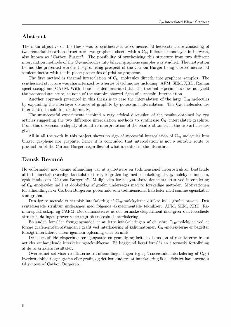
The results from their calculations can be seen in figure 2.7. Figure 2.7b and 2.7c are the electronic
band structure for graphene and a monolayer of C60, respectively. They note that a similar result as
the calculated band structure for the intercalated compound (figure 2.7a), can be obtained by simply
merging that of graphene and C60, and aligning the Fermi levels. Such a simple approach does (of
course) not give the right results, as some interaction between the graphene layers and the C60 layers
must be expected. Valence electron density calculations from the same paper does indeed show changes
compared to pure graphene and C60, with a charge transfer towards the C60-layer. The charge transfer
can be understood from a simple consideration of the π states of planar graphene and spherical C60.
Even though the carbon atoms in both graphene and C60 are sp2-hybridized, the curvature of the
C60 molecule introduces a s-orbital component to the π-state, which are not pure pz-orbital as for a
perfectly planar graphene sheet. Hence the C60 π-state is lower in energy and a finite charge transfer
from graphene to C60 must be expected. Saito and Oshiyama 75 does not estimate the size of the
charge transfer. This can be determine from a simpler system, with a monolayer of C60 deposited on a
graphene sheet, and indeed many such studies have been performed, both structural44, electrical16;82
12
C60 Intercalated Bilayer Graphene Chapter 2. Background
and theoretical82 . Cho et al. 16 determines the direct HOMO-LUMO gap of C60-molecules on an
epitaxial grown graphene on SiC to be ∼ 3.5 eV. They report reduced charge transfer from graphene
to C60, when comparing with C60 on various metallic substrates. Furthermore it is confirmed that
the C60-molecules forms a hcp monolayer on graphene, with a nearest neighbour distance of ∼ 1 nm,
comparable to that of solid C60. The charge transfer from graphene to a C60-molecule is of the order
of 0.01 electron84, hence the Fermi energy is expected to still lie within the band gap of the C60
monolayer, as calculated by Saito and Oshiyama 75 .
(a) (b) (c) (d)
Figure 2.7: C60 intercalated graphite (a) Energy band calculation of the C60C32 structure, arrangedas seen in (d). (b) Energy band calculation for C32 unit cell. (c) Energy band calculation for a C60
molecule. (d) Proposed arrangement of the intercalated C60 molecules between graphene layers ingraphite. (a), (b), (c) and (d) adopted from Saito and Oshiyama 75
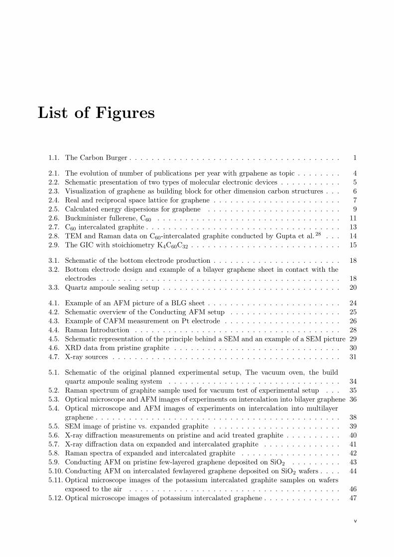
The first group to directly intercalated C60 into graphite were Gupta et al. 28 ‡. They show that
by heating C60 powder and graphite powder to 600C for 2 weeks, a highly ordered stage-1 GIC is
produced. This observation is supported by the Transmission Electron Microscope (TEM) and Raman
measurements seen in figure 2.8. Figure 2.8a is a High Resolution Transmission Electron Microscope
(HRTEM) image of pristine graphite. HRTEM image of the GIC where each individual C60 molecule
are visible and one marked by an arrow is presented in figure figure 2.8b. Gupta et al. 28 observe an
increased interlayer distance, marked by the two parallel lines , measured to 1.27 nm. The enhanced
interlayer distance was estimated to 1.29 nm, and is in good agreement with the observed distance
in figure 2.8b. The synthesized material showed hexagonal symmetry obtained from selected area
diffraction data (not shown here, but will be discussed in section 5.5).
The Raman data for the intercalated compound can be seen in figure 2.8c. Assigning the three
peaks from right to left in the same way as Gupta et al. 28 , the first is the G-peak for graphite, up-
shifted from the usual 1582 cm−1 to 1589 cm−1, due to electron transfer from graphite to C60. This
postulate is in good agreement with the small charge transfer expected by Saito and Oshiyama 75 .
The same charge transfer down-shift the peak for pristine C60 from 1469 cm−1 to 1446.1 cm−1. The
electron transfer is expected to partially fill the t1u level, making the C60 layers highly conductive.
Lastly the broad peak at 1370 cm−1 is a D-peak, indicating slightly defected graphite. From these
data Gupta et al. 28 conclude successful intercalation of a highly ordered compound of C60 intercalated
graphite.
‡Albeit they claim to use graphite they do use exfoliated graphite. But these considerations are not important at
present, but will be discussed later on.
13
Chapter 2. Background C60 Intercalated Bilayer Graphene
(a) (b) (c)
Figure 2.8: Results obtained by Gupta et al. 28 . (a) HRTEM image of graphite. (b) HRTEMimage of stage-1 C60 intercalated graphite, with a individual C60 molecule marked by the arrow andthe interplanar distance measured to 1.27 nm. (c) Raman spectrum of stage-1 C60 intercalatedgraphite, showing a small D peak around 1370 cm−1, a down shifted C60 peak at 1446.1 cm−1 anda up shifted G peak for graphite at 1589.1 cm−1.
The main part of the experiments in this project will build on these experiments, in the attempt
to produce a 2D all-carbon semiconductor. The results will be presented and discussed in section 5,
where the results obtained by Gupta et al. 28 will be more critical reviewed, partially based on the
results obtained in this project.
2.4.2 Potassium and C60 co-Intercalated Bilayer Graphene
Another approach towards C60-intercalated graphite, is through an intermediate product of potassium
intercalated graphite, C8K. This were demonstrated by Fuhrer et al. 23 in 1994. The C8K precursor
was synthesised by two-zone thermal intercalation of potassium58. The two-zone method is charac-
terized by two connected chambers, one containing the potassium and one the graphite. Heating the
chambers controlling the temperature gradient between the two sides, the stage number of the GIC
can be controlled with high precision, as is is temperature dependent58 . For the stage-1 GIC the
temperature different should be hold at a minimum, but non-zero to avoid to much adsorption on
the surface of the graphite17 . The resulting structure with stoichiometry C32K4C60 were prepared
by immersing the C8K precursor in a 80C saturated solution of C60 in dry benzene. The proposed
arrangement of the potassium atoms and C60-molecules in the interlayer sites of the graphite can
be seen in figure 2.9b. Fuhrer et al. 23 only conduct transport characterization of the synthesized
structure. These measurements showed that the sample were superconducting after annealing, with a
transition temperature of 19.5 K, close to that of K3C60 structure. Before annealing of the sample, the
sample showed no sign of superconductivity above 4.2 K. They postulate that the C60 and benzene
co-intercalate into C8K precursor, and only upon removal of excess benzene a superconducting phase
is formed. The relative high resistivity below the transition temperature, not going to zero, is assigned
to only fractional superconductivity in the sample.
The measured superconductivity was predicted by Saito and Oshiyama 75 around the same time
as the experiments. The calculation on the electronic band structure for C32K4C60, is presented in
figure 2.9a. It is seen that the band structure is similar to that of pure C60 GIC, except that the Fermi
14

C60 Intercalated Bilayer Graphene Chapter 2. Background
(a) (b) (c)
Figure 2.9: The GIC with stoichiometry K4C60C32. (a) Electronic band structure calculation bySaito and Oshiyama 75 (b) Suggested arrangement of the potassium atoms (small decorated spheres)and C60-molecules (large open spheres) in the graphite. Adapted from Saito and Oshiyama 75 .(c) Low temperature measurement by Fuhrer et al. 23 on the GIC, showing superconductivity withtransition temperature, Tc = 19.5 K.
energy lies around the original t1u-level from the C60-molecule. This is the same effect seen in the
superconducting alkali metal intercalated C60 crystal, M3C60, which can explain the similar transition
temperatures.
Fuhrer et al. 23 argue that the seen superconductivity indeed arises from the intercalation product
and not a K3C60 phase in the sample. The postulate is that C60-molecules probably would form K6C60
when reacting with potassium in excess, which is an insulating phase2;88, and not the superconducting
K3C60 phase. Furthermore they state that it is unlikely that a K3C60 phase would account for the
reproducibility they observe for all their samples. To confirm whether the superconductivity is due
to a K3C60 or C32K4C60 phase they state that XRD and Raman measurements were in the making.
These measurements are a necessity for eliminate either of the two structures. Unfortunately these
measurements were never published.
The second part of this thesis will build on these findings, with focus on easing the intercalation
of C60 into bilayer graphene through the intermediate product C8K3. The results obtained will be
presented and discussed in section 5, and compared to the results obtained by Fuhrer et al. 23 .
15


Chapter 3
Experiments
The experimental part of the thesis is presented to give an overview of techniques used
in the attempt to prepare C60 intercalated bilayer graphene and the experimental difficulties
encountered. The synthesis of C60 intercalated bilayer graphene, is a two-step process, namely
production of bilayer graphene on wafers and the intercalation of C60. The production of co-
intercalation of potassium and C60 into BLG, is done by preparing the C8K-precursor for the
C60-intercalation. For further details see appendix A, which is a step-by-step presentation of
the optimized experimental procedures.
3.1 Basic Device Fabrication
Before the intercalation experiments, devices containing BLG sheets contacted by electrodes are pro-
duced. The idea was to produce in-plane electrodes on a SiO2 wafer and then deposit graphene/gra-
phite on-top. The details are presented below.
3.1.1 Bottom Electrode Production
Bottom electrodes were produced in two different ways. Either optical lithography, for which shadow-
masks were designed using the software Clewin 486 and produced by Delta Mask47. Or electron beam
lithography (EBL), where design files were produced with the software DesignCad 3D Max33.
Photo-resist (or PMMA for EBL) were spin cast on silicon wafers with 285 nm layer of SiO2 (the
optimized oxide layer thickness for making graphene visible in an Optical Microscope, see section 4.1
for further details). After lithography the wafers were etched with a hydrofluoric acid etching mixture,
provided by Sigma Aldrich78, with a well-known etching rate. An E-gun metal evaporator was used
for metal deposition, and the photo-resist was lifted-off leaving behind the etched down electrodes.
Figure 3.1 is a schematic representation of the bottom electrodes production.
The electrode metal chosen was Platinum as its electrical properties are expected to be more stable
than e.g. gold, after exposure to elevated temperatures for longer time (600C for up to two weeks
was needed for the intercalation synthesis28). The metal to SiO2 adhesion was increased by deposition
of a thin layer (5 nm) of Titanium prior to Pt. Picture 3.2a shows the final results, including the
designed coordinate system, with the light areas being the Pt electrodes and the dark blue SiO2.
17

Chapter 3. Experiments C60 Intercalated Bilayer Graphene
SiO2
SiSpin cast
photoresist
Lithography
Etching
Metal
deposition
Lift-off
Figure 3.1: Schematic of the bottom electrode production and the different production processesused, being in right order; photoresist deposition, lithography, ething, metal evaporation and lift-off.
3.1.2 Pristine Bilayer Graphene
A wafer prepared as described above, is cleaned with acetone, methanol and IsoPropyl Alcohol (IPA),
and ashed for 5 minutes in a plasma oven. Deposition of graphene on the wafer is done using the
technique developed by Novoselov et al. 59 , where tape is used to mechanical cleave flakes of natural
graphite. The number of graphene layers per flake is reduced by repeatedly sticking together and
peeling off the tape. The hopefully few layer graphene sheets can be transferred to the wafer, simply
by putting the graphene covered side towards the wafer. The tape can be peeled off by heating the
wafer to 70C until the tape is released, leaving behind a minimal amount of glue on the sample.
(a) (b)
Figure 3.2: Sample design and preparation. (a) Bottom electrodes and coordinate system. Darkareas are SiO2 and light are the Platinum electrodes. (b) An example of a (small) bilayer graphenesheet, marked by the red circle, visible on SiO2 and invisible on Pt. Pictures are taken with anOlympus optical microscope.
3.1.3 Expanded Bilayer Graphene
In order to ease the future intercalation step, the graphite interlayer distance was attempted increased,
by preparing expanded graphite. It is reported that treating natural graphite with a mixture of sul-
phuric acid and nitric acid (4:1) for 16h, followed by a shock-heat-treatment (1050C for 15s) produce
expanded graphite13. As this acid mixture is known to dissolve some noble metals it was replaced with
fuming sulphuric acid (oleum) as the bottom electrodes consisted of noble metal platinum. Further-
18

C60 Intercalated Bilayer Graphene Chapter 3. Experiments
more is H2SO4 a known intercalant in graphite3, and hence the treatment with the highly concentrated
sulphuric acid were expected to give similar results as the acid mixture. However it turned out im-
possible to do the acid intercalation on a substrate as intercalation between the graphene sheets and
the surface resulted in almost all sheets washed off or was dissolved in the solution.
After these initial results, the acid treatment was conducted prior to deposition on the substrate.
This was done by soaking natural graphite in oleum for at least 12h, followed by rinsing in millipore
water. Attempts towards mechanical cleave the acid treated graphite with the tape technique were
unsuccessful, as the graphite did not stick to the tape, indicating change in the surface chemistry.
This and the observation that the acid treated graphite kept sticking to the metal tweezer, could
indicate charges on the surface. Further indication of successful intercalation (or at least some kind of
reaction), was the weight of the graphite pieces after acid treatment, which approximately doubled.
The vain attempt of wafer depositing the acid treated graphite, inspired the production of ex-
panded graphite prior to wafer deposition. The initial hope of doing the expansion of the graphite
after deposition on wafers was that a thickness increase of the graphite sheets could be detected using
AFM, see section 4.2. Instead was the acid treated graphite heated to 600C for 1 min in a nitrogen
atmosphere. Expansion of the graphite flakes were observed as the graphite grew into a worm-like
structure (referred to as expanded graphite). Deposition of the expanded graphite with the tape tech-
nique was possible, indicating that the before expected charges in the acid treated graphite vanished.
Further discussion and results on the different graphite samples in presented in section 5.
3.2 Synthesis of C60 Intercalated Bilayer Graphene
After production of BLG samples, the experiments on C60 intercalation could be started. The inter-
calation process used in this project is highly inspired by the work by Gupta et al. 28 .
3.2.1 Intercalation
The graphene sheets prepared as described above and C60 powder, were put in a quartz ampoule
(dimensions 1x10 cm). The ampoule was evacuated (for atleast 1 hour) using a turbo-pump, reaching
a vacuum < 10−5 mbar, see figure 3.3b for the turbo-pump setup. When a satisfactory high vacuum
was reached the ampoule was sealed using a oxy-propane burner bought from Arnold Gruppe27, see
figure 3.3a for the sealing process. The sealed and evacuated ampoule containing the graphene covered
wafer and C60-powder was heated to 600C for two weeks. Removal of excess C60-molecules adsorbed
on the surface of the wafers, were attempted with either heat treatment in a continuous nitrogen flow
or dispersion in acetone followed by drying the wafer at 80C to remove excess acetone.
Experiments with C60 intercalation into expanded graphite were conducted, in the same way as
described above.
19

Chapter 3. Experiments C60 Intercalated Bilayer Graphene
(a) (b)
Figure 3.3: Quartz ampoule sealing setup. (a) Close-up of the quartz burner sealing a pumped downquartz tube. (b) An overview of the experimental setup, including the quartz burner, turbopumpand adapter for the quartz tubes.
3.3 Synthesis of C60 Intercalated Bilayer Graphene from C8K Pre-
cursor
Another approach towards C60 intercalated bilayer graphene, synthesizing the structure C60C32K4, was
suggested. The idea of using potassium intercalated BLG, C8K, as a precursor for C60 intercalation,
was obtained from Fuhrer et al. 23 . The intercalation of potassium is carried out as described by Nixon
and Parry 58 . Apart from the solution based intercalation suggested by Fuhrer et al. 23 , an alternative
approach where all intercalation processes were done thermally was suggested.
3.3.1 Intercalation of Potassium
A quartz tube was prepared with a BLG sample, along with a small piece of solid Potassium (∼ 0.03
mg). The otassium was washed with heptane to remove paraffin and the oxide covered parts was cut
away. The quartz tube was pumped down to a pressure of approximately 10−6 mbar, and was sealed
off with an oxy-propane burner. The sealed quartz tube was heated to 300C for three hours, which is
reported to yields a stage-1 intercalation product between potassium and graphite. For intercalation
of graphite the stage-1 product can be verified by the graphite changing color from gray to gold.
No temperature gradient was induced while doing the intercalation as only stage-1 compounds was
desired.
In stead experiments on removing potassium adsorb on the wafer, were done by creating a thermal
gradient inside the sealed quartz tube, after the intercalation experiment was conducted. The part of
20

C60 Intercalated Bilayer Graphene Chapter 3. Experiments
quartz tube containing the wafer was put on a heating plate set to 100C, hopefully not resulting in
de-intercalating of potassium, only desorption.
3.3.2 Solution Based Intercalation of C60 into C8K-precursor
A saturated solution of C60 in dry benzene was prepared. The saturation can be verified by the strong
purple color of the solution. The produced C8K precursor on wafer was immersed in the solution
and heated to 80C for 24 h. Fuhrer et al. 23 report that the samples needs to be annealed in order
to remove excess solvent, and measure superconductivity. Due to different problems, which will be
discussed in chapter 5, this were never done, but should be kept in mind if the encountered problems
are solved, and transport measurements is conducted.
3.3.3 Thermal co-Intercalation of C60 and Potassium
Another approach towards the C60C32K4 structure was attempted. A sealed quartz tube containing
C60-powder, potassium and a graphene wafer sample was prepared. The sealed quartz tube was first
heated to 300C for three hours to intercalate the potassium and expanding the BLG/FLG sheets.
Afterwards was the quartz tube heated to the 600C for the 2 weeks, needed for the C60 intercalation
to take place.
21


Chapter 4
Characterization Techniques
Throughout the course of the thesis a variety of techniques were used, namely Optical Mi-
croscopy, Atomic Force Microscope (AFM), Conducting AFM (CAFM), Raman Spectroscopy,
Scanning Electron Microscopy (SEM) and X-ray Diffraction (XRD). Below are a short intro-
duction to every technique and a description of how the data manipulation was carried out.
4.1 Optical Microscopy
Optical microscopy is optimal for the initial search for bilayer graphene deposit on SiO2/Si wafers.
Even though few layer graphene sheets are transparent in visible light, they can be seen in the optical
microscope with careful choice of wafer. The wafer of choice is silicon with 285 nm of oxide layer.
This is due to a weak interference-like contrast between graphene and the SiO2 layer, compared to an
empty Si wafer. Hence the thickness of the oxide layer is very important and many experiments have
been conducted to optimize the contrast8;24. Thus all wafers used in this project have the optimal 285
nm thick SiO2 layer. Figure 3.2b is a typical example of a BLG sheet visible on SiO2 but invisible on
the Pt electrode.
Non-destructive measurements and the possibility to search large wafer areas for graphene sheets
relatively fast are the biggest advantages of the optical microscope. The disadvantage is that few
conclusions can be made from the pictures, and as such the method is mostly relevant as a sheet
detection tool.
4.2 Atomic Force Microscopy
The Atomic Force Microscope (AFM) is characterized by the use of a mechanical probe to scan surfaces
for nano scale information about the morphology of the surface7.
Different modes of operation can be employed when using AFM, some of these are: Contact mode,
non-contact mode and the intermediate tapping mode. In all of the modes it is the atomic forces
between tip and surface that are registered, or more correctly the Van der Waal forces modelled by
23

Chapter 4. Characterization Techniques C60 Intercalated Bilayer Graphene
the Lennard-Jones potential36 equation 4.1.
U(r) = 4ǫ
[
(σ
r
)12−
(σ
r
)6]
(4.1)
Where ǫ is the depth of the LJ potential well and σ is the distance between tip and sample where the
potential is zero.
All measurements in this project are conducted with tapping mode, where the vibrating cantilever
is placed in exactly such a height that the tip taps the surface with a specific resonance while scanning.
The resonance of the cantilever is kept constant by changing the distance to the surface, correcting
for either height differences or change in surface stickiness. Two AFM apparatus were used, one being
a Veeco Multimode 8 and the other a Veeco Dimension Icon. The difference between the quality of
the images obtained by the two types of AFMs is not significant hence will not be distinguished.
All AFM data processing was done with the program Gwyddion56. Figure 4.1a is an AFM picture
of the sheet seen in figure 3.2, while figure 4.1b is a line height profile from the SiO2 area to the
graphene, with the height of the bilayer graphene flake estimated by a step function to approximately
1.2 ± 0.1 nm. AFM pictures presented throughout the thesis are all manipulated, with built-in tools
in the Gwyddion software, correcting for data acquisition induced defects, e.g. non-planar surfaces.
The highest advantages of using an AFM as the main characterization tool in this project, are
unlimited access (I was one of very few users) and the relatively immediate and direct indication of
intercalation. As a rule of thumb, the height of a SLG on SiO2 is approximately 1 nm and the interlayer
distance in MLG (and graphite) is approximately 0.3 nm. From both the theory and the experimental
work, it is expected that the interlayer distance increases to ≥ 1 nm after C60 intercalation, increasing
the thickness of the graphene sheet significantly, see section 2.4.
(a) (b)
Figure 4.1: (a) AFM picture of the sheet seen in 3.2. The orange part is the SiO2 surface andthe darker more rough surface is the Pt electrode. (b) Height profile of the line seen in (a). Heightestimated by step function fit to 1.2± 0.2 nm.
24

C60 Intercalated Bilayer Graphene Chapter 4. Characterization Techniques
4.3 Conducting Atomic Force Microscopy
For electrical measurements, an AFM is modified so the tip acts as an electrode. A schematic overview
can be seen in figure 4.2. The advantages of this technique are the relatively fast data acquisition∗
and the possibility of probing the sample at different sites.
Special AFM tips made conductive with a coat of platinum, produced by µMasch 55 , were used for
the conductance measurements. A voltage supplier (Keithley 2400 Source-Meter) was connected as
seen in figure 4.2, with a 1 MΩ resistor before the tip, minimizing the current passing through. The
conducting AFM tips could not tolerate a current higher than 100 nA. The current was measured with
a Keithley 6514 System Electrometer, with a measurement sensitivity of ±100 aA. The experimental
setup system was controlled in Labview 201034. All I-V-curves in this project were taken with a bias
voltage interval from −5 mV to 5 mV in 200 steps.
1MΩ
Conductive AFM Tip
SiO2
Si
Graphene/Graphite
Pt Electrode
Figure 4.2: Schematic overview of the Conducting AFM setup. The system consists of a conductiveAFM tip in contact with the sample. A voltage supplier is connected with a 1 MΩ resistor beforethe tip, minimizing the current set through the tip. By engaging the tip at different sites of thesample I-V curves can be conducted.
Figure 4.3 shows CAFM data where the AFM tip is engaged and in contact with a bottom electrode,
basically short circuiting the system. Figure 4.3a shows raw data from 7 voltage sweeps from -5 mV
to 5 mV. It is seen that the I-V curve in this interval is linear and obeys Ohms law, and hence is a
conductor as expected. Data manipulation is done by taking the average of all the sweeps, followed
by a linear fit to this curve, the result of which can be seen in figure 4.3b.
The CAFM data presented in the results chapter contains measurements on different sites, twice on
the electrode and a couple of times on the sheet. The results are collected and presented in a table
similar to table 4.1. The average conductance is read directly from the linear fit as the slope, while
the resistance is calculated by taking the inverse of the slope. The resistance measured is a serial
resistance, originating from the experimental equipment, and is on its own not informative. Taking
the difference between a short circuit measurement (electrode) and one on a sheet, could potentially
give information on the electronic properties of the sheet. But as will be discussed below and in further
details in section 5 this is not as straight forward as first expected.
Conductance measurements on BLG in contact with an electrode was not expected to alter the
total resistance within the detection limit, as the BLG has high charge carrier mobility. Measuring on
a C60-intercalated BLG, where a band gap is introduced to the BLG, hopefully lowers the conductance
enough to be detectable. The precision of the equipment and the averaging over several sweeps should
give good statistics on the measurements, which for individual measurements is the case. The linear fit∗Within half an hour, a sample can be mount and measured
25

Chapter 4. Characterization Techniques C60 Intercalated Bilayer Graphene
-0.006 -0.004 -0.002 0.000 0.002 0.004 0.006-2.00E-009
-1.50E-009
-1.00E-009
-5.00E-010
0.00E+000
5.00E-010
1.00E-009
1.50E-009
2.00E-009
Cur
rent
[A]
Voltage [V]
Sweep 1 Sweep 2 Sweep 3 Sweep 4 Sweep 5 Sweep 6 Sweep 7
(a)
-0.006 -0.004 -0.002 0.000 0.002 0.004 0.006-2.00E-009
-1.50E-009
-1.00E-009
-5.00E-010
0.00E+000
5.00E-010
1.00E-009
1.50E-009
2.00E-009
Cur
rent
[A]
Voltage [V]
Average of Sweep 1-7 Linear Fit of Averaged Data
(b)
Figure 4.3: CAFM measurement on a Pt electrode. (a) The raw data from 7 voltage sweeps from-5 mV to 5 mV. The I-V-curve shows linear characteristics corresponding to a conductor, as expectedfor the Pt electrodes. (b) Average of the 7 sweeps in (a) and a linear fit to this curve.
has a standard error to the slope of 4.6 · 10−4 µS, or a precision to the third decimal. However as will
be seen in the section 5 the variation from measurement to measurement on the same sample varies
with the first decimal. This variation will be discussed in further detail when the relevant data is
presented, thus only a summary of the argument is given here. The possibility of CAFM tip topology
changing after having been engaged into the sample is relatively high, which might change the contact
area between tip and sample, hence the contact resistance. Also local variations in the sample might
alter the resistance undesirably. Thus a significant change in the resistance between two subsequent
measurements on the same sample at the same place with the same tip might occur. The difference is
seen to be larger than the precision on individual measurement. Hence the standard error will only be
presented in the tables for good measure, but as such is not informative as large variations between
each engagement makes the extraction of sheet resistances lower than 0.1MΩ impossible.
Table 4.1: Data from the linear fit in figure 4.3b
Avg. Conductance Avg. Resistance0.3220 ± 0.0005µS 3.106 ± 0.005MΩ
4.4 Raman Spectroscopy
Raman Spectroscopy is a strong tool when investigating the physical properties of a FLG-sheet, as the
so-called D and G peaks are highly dependent on the number of layers, doping, disorder and phonon
distribution. In order to understand this dependency, a deeper knowledge of Raman spectroscopy on
graphene is needed, but initially general Raman scattering will be introduced.
Irradiation of matter with monochromatic light can lead to different processes, i.e. the light being
transmitted, absorbed or scattered. The Raman process is in general that of inelastic scattering
of monochromatic light with matter62, as opposed to Rayleigh scattering where the light frequency
remains unchanged. The change in frequency is due to the excited electron inducing a phonon at the
26

C60 Intercalated Bilayer Graphene Chapter 4. Characterization Techniques
expense of energy.
For Raman spectroscopy the light is usually in the visible, near infra-red or near ultraviolet range,
depending on the material measured. All Raman spectra in this project were conducted with a
wavelength of λ = 514 nm and a spot size of roughly 1 µm.
Raman spectroscopy on graphene was early discovered to be a strong tool when characterizing
the properties of the material22. Even though Raman spectroscopy is a very popular technique,
misinterpretation and disagreement of peak assignment is still very common in the literature21 . The
paper by Ferrari and Basko 21 from 2013 reviews the latest development in Raman spectroscopy on
graphene and proposes a self-consistent terminology, in order to minimize peak interpretation mistakes
in the future. All Raman data in this thesis will be processed within the terms of this terminology.
The processes giving rise to Raman peaks can be visualized by a model as seen in figure 4.4b.
Here the origin of five different peaks are illustrated by different scattering processes. In the suggested
process responsible for the G peak, an electron is excited by absorption of a photon. The excited
electron relaxes back by emission of a standing phonon and a photon. In the presence of defects, the
wave vector of the emitted phonon can be non-zero, as the electron can scatter back on defects, as
illustrated for the D and D’ peaks. Hence the relative intensity of these peaks gives information on
the number of defects in the graphene sheet. Lastly a two phonon process where the conservation of
momentum is fulfilled by emission of two phonons with opposite wave vectors, leads to two peaks,
namely 2D and 2D’.
Raman data are plotted in terms of the Raman shift, defined as the difference between the incident
and scattered photon, and are by historical reasons given in wave numbers [cm−1]. Raman peaks can
be assigned to specific processes, with the most important being the E2g responsible for the G-peak,
see figure 4.4c for a visualization of the phonon mode.
A typical Raman spectrum for pristine graphene can be seen in the upper part of figure 4.4a, while
the lower part is from a graphene sheet with many defects. Such Raman spectra gives immediate infor-
mation about quality and number of layers. The D peak is due to disorder in the sheet, independent on
defect types, being e.g. missing atoms and edges, as this peak originates from Raman processes only
conserving momentum by scattering on defects. The absence of the D peak in the pristine graphene
indicates high purity. The relative ratio between the G and 2D peak, gives us information about the
number of layers. For graphene the 2D peak is more intense, whereas for three layers and up the G
peak dominates. For BLG the ratio is approximately one.
Figure 4.4d shows a Raman spectrum of a BLG sheet (the same sheet as seen in fig 3.2). Here
it is indeed seen that the G and D peak are present in a 1:1 ratio, confirming that the sheet consist
of two layer of graphene in a Bernal stacking. Furthermore the very weak D peak indicate the high
quality of the graphite used. Informations on the peak, such as position, standard error and FWHM,
are extracted by fitting a Voigt function, using the software OriginPro64.
4.5 Scanning Electron Microscopy
For higher resolution images than an optical microscope can produce, a Scanning Electron Microscope
(SEM) was used. The high resolution is the biggest advantage of this technique, but the disadvan-
27

Chapter 4. Characterization Techniques C60 Intercalated Bilayer Graphene
(a) (b)
(c)
1500 2000 2500 3000 35000
2000
4000
6000
8000
10000
12000
14000
16000
18000
20000
Ram
an In
tens
ity
Wavenumber (cm-1)
P3F22
(d)
Figure 4.4: (a) Example of Raman spectra of high quality graphene (upper) and defected graphene(lower). (b) Proposed processes behind the peaks seen in (a). (c) The phonon mode responsiblefor the G peak. It is seen that this mode is active in the graphene. (d) Raman spectrum of bilayergraphene, showing the high quality of the graphene used in the project. (a) and (c) adapted fromFerrari and Basko 21 , (b) Adapted from Basko et al. 5 .
tages, where the most serious are the destruction of graphite and deposition of amorphous carbon by
irradiation with the electron beam, minimizes the usability of this technique.
The principle behind a SEM is to take advantage of the wave-like nature of electrons, in a similar
way as an optical microscope uses light. Figure 4.5a is a schematic representation of the principal
behind SEM. Electrons are accelerated in the electron gun, from an electron source to an anode, and
focused down trough some magnetic lenses. Before reaching the sample the electron beam passes
through deflection coils, which can scan the beam over the sample and correct for astigmatism. Two
options are available when acquiring the SEM picture, both Back-Scattered Electrons (BSE) and
Secondary Electrons (SE) can be collected. All images in the project are recorded with BSE. Figure
4.5b is a SEM image of a piece of pristine graphite used in the project.
As the electron beam is destructive to carbon samples, low voltage imaging is preferable. All
images in this thesis were taken with an acceleration voltage of 10 kV, which is not very low, but the
minimum of the Jeol JSM 632OF apparatus used.
28

C60 Intercalated Bilayer Graphene Chapter 4. Characterization Techniques
Secondary Electron Detector
Electron Gun
Condensor Lens
Condensor Lens
Deflection Coils
Back-Scattered Electron DetectorBack-Scattered Electrons
Secondary Electrons
(a) (b)
Figure 4.5: Scanning Electron Microscope (a) Schematic representation of the principle behind aSEM. An electron beam is focused by a couple of magnetic lenses, before reaching the deflectioncoils. The deflection coils correct for astigmatism of the beam and are responsible for scanning thesample. (b) A SEM picture of a pristine graphite piece. Image is produced by collecting the BSEelectrons.
4.6 X-ray Diffraction
Change in the interlayer distance is a strong evidence of successful intercalation, as discussed in the
AFM section. However the experiments with expanded graphite were all conducted before deposition
onto a substrate, excluding AFM as a useful technique. Instead X-ray Diffraction (XRD) measurements
on the graphite pieces was conducted. XRD is normally used for measuring the Bragg reflections from
crystals, thus yielding information on the crystal structure and lattice parameters. In crystals the
periodic lattice planes can be regarded as semi-transparent mirrors, which give rise to backscattering
of an incident electromagnetic beam. Only at certain incident angels are the backscattered light in
phase, giving rise to constructive interference. This can be described by Braggs law, eq. 4.2, saying
that the incident wavelength, λ, equals the lattice plane separation, d, times sine to the incident angel,
θ,
nλ = 2d sin θ (4.2)
From this simple equation each diffraction peak in a XRD spectrum (which is given in terms of
2θ) can be contributed to a specific plane spacing. It is possible to assign each individual peak to a
lattice plane, albeit very tediously, especially if the crystal structure is unknown and multiple crystal
phases are present. As the technique was used for detection of intercalation, only the plane distance
was of importance, hence crystal structure information will not be extracted from the XRD data.
The highly planar structure of graphite gives rise to one very prominent Bragg reflection from the
(002)-plane, remembering the unit cell of graphite contains two atomic planes. The plane distance
of 3.5 nm for pristine graphite would give a prominent peak at 2θ = 26.6 with an x-ray wavelength
of λ = 1.54 Å, as seen in figure 4.6. Other peaks present are due to reflection from other lattice
29

Chapter 4. Characterization Techniques C60 Intercalated Bilayer Graphene
planes, but are as such not relevant for this thesis as intercalation would be visual by studying the
(002)-reflection only. In figure 4.6 these peaks are not visible, due to the high intensity from the (002)-
reflection, which also is the origin of the second peak seen, namely the second order of the (002)-peak.
To analyse the peak, Voigt (combination of Gauss and Lorentz) functions are applied. The choice is
dependent on the source but for the two kinds used in this project a Voigt distribution was suitable.
The next section further describes the two different sources. The fitting was done with the software
OriginPro64, and the standard errors were hence extracted from these fits. The calculated standard
error for the peak position was for many of the peak fits smaller than the precision on the specified
x-ray wavelength. Thus for the peaks with fitted standard error lower than the apparatus precision,
the uncertainty on position is based on the x-ray source and not the fit.
10 20 30 40 50 60 70 800
200000
400000
600000
800000
1000000
1200000
1400000
Inte
nsity
[a.u
.]
2
Pristine Graphite Lorentz Fit to peak at 26.64 Lorentz Fit to peak at 54.75 Cumulative Fit Peak
Figure 4.6: XRD data from pristine graphite. The high intensity peak at 2θ = 26.64 is the(002)-reflection, while the second visible peak is the 2nd order of this peak.
The X-ray Sources
Two different types of x-ray sources were used for the diffraction measurements. One type was a
Bruker D8 X-ray Diffraction system10. This x-ray source is a classic copper anode, which produces
Kα radiation with λ = 1.54 Å. The principle behind the design can be seen in figure 4.7a. Electrons
are accelerated from, in this case, a wolfram filament to a copper anode. When the electrons hit the
copper anode, they are decelerated due to interaction with the nuclei, sending out electromagnetic
radiation. This type of radiation is called Bremsstrahlung and is a broad spectrum of wavelengths.
Two high intensity x-ray peaks are characteristic for copper, namely Kα and Kβ. These two peaks
originate from electron-electron scattering, where the high energy electrons hitting the copper anode
kick out a K shell electron. Higher energy electrons then relax back to the vacant by sending out a
photon with a very distinct energy. The nomenclature is as follows: The capital letter denotes what
shell the core electron relaxes back into (K,L,..), whereas the subscript denotes whether it comes from
the shell closets in energy (α) or 2nd closest (β) etc. By filtering away all other energies, a high
intensity and low-energy-dispersive x-ray beam can be produced.
Other x-ray measurements were done in MaxLab Lund, beam-line 911-1 (Cassiopeia), by a student
group following an experimental course on x-ray techniques, where I was fortunate enough that they
used some of my GICs as course samples. The synchrotron source is a so-called wiggler, see figure
30

C60 Intercalated Bilayer Graphene Chapter 4. Characterization Techniques
Water CoolingElectron Beam
X-rays
Copper Target
Wolfram Filament
(a) (b)
Figure 4.7: X-ray sources (a) Schematic representation of the principle behind a Copper anode (b) Awiggler x-ray source. A electron is accelerated in opposed magnetic field, emitting light under each ac-celeration. Picture adapted from: http://www.psi.ch/media-/the-swiss-light-source-sls
- July 2013
4.7b. This source produces x-rays with a wavelength of 1.048 Å, by accelerating charged particles
(electrons) through a series of opposed magnetic fields, emitting x-rays for every acceleration. The
wiggler holds the advantage over, the normal copper anode, of producing a much higher intensity x-ray
beam, hence having better resolution in the low angle regime. This makes the synchrotron source ideal
when measuring on graphite intercalation compounds (GIC) with expected high interlayer distance.
31


Chapter 5
Results and Discussion
Chapter 5 begins with a description of some of the problems encountered while working on
the project. Next the results obtained throughout the course of the project are presented and
discussed. The result presentation is divided into three main parts, being thermal intercalation
of C60 in few-layer graphene, C60 intercalation into bulk graphite and finally co-intercalation of
Potassium and C60.
5.1 Progress of the Project
The main objective of the project was to intercalate C60-molecules in-between two graphene layers, but
before these experiments could be conducted a intercalation system was build. The initial approach
was to use a small vacuum chamber with a heating element inside, see figure 5.1a for a schematic
drawing. The idea was to use the heating element to heat a graphene sample and C60 powder to the
600C required for the intercalation inside the vacuum chamber. This setup never became operational
due to a variety of things. First of all, the basic design had at least one major flaw, namely the
continuous need for pumping. Hence it would be very tricky, if not impossible, to create the high
C60 vapour pressure required for the intercalation to take place. Furthermore the chamber has a lot
of leaking sites, e.i. only a vacuum of 10−1 mbar could initially be created. After three months of
consecutive attempts to leak detect and seal, the chamber was finally satisfactory sealed for a test run
of 7 days with the heating element powered up. After 5 of the 7 days, a leak appeared while heating to
600C, and the electrodes and the heating plate oxidized and consequently died. It was not possible
to repair the heating element, and this experimental setup was finally banned. After consulting the
literature, where the usual approach was to pump down a quartz tube and seal it, a similar setup
was build, see schematic in figure 5.1b. After 1 month where several gas burners and gas types were
tested∗, an oxy-propane burner with four nozzles from Arnold Gruppe27 was chosen, see figure 3.3a.
A turbo pump capable of creating a vacuum of 1 ·10−6 mbar was used. Thus almost half way through
the project the actual experiments were started.∗Quartz melting point is beyond the 2000C, so specialized tools were needed before the experiments could be realized
33

Chapter 5. Results and Discussion C60 Intercalated Bilayer Graphene
Vacuumpump
PressureGauge
Thermocouple
(a)
PressureGauge
Vacuumpump
(b)
Figure 5.1: The two different experimental systems attempted build in the project. (a) Theunsuccessful vacuum oven, consisting of a heating element controlled by a voltage supplier and athermocouple. The vacuum was created with a vacuum pump and measured with a pressure gauge.(b) The successful setup, consisting of the quartz tube connected to a turbo pump, capable ofcreating a vacuum < 10−5 mbar. The quartz tube can be sealed by an external gas burner.
5.1.1 Testing the Quartz Tube Setup
First step after completing the quartz tube evacuation and sealing setup, was to verify that a graphene
sheet could survive the heat treatment, i.e. if the quartz tubes did indeed hold a high vacuum (< 10−5
mbar). A tube containing multilayer graphene was evacuated and heated to 600C for 2 weeks. Figure
5.2 shows the Raman spectrum taken subsequent to the heating. From the absence of a pronounced
D-peak (around 1400 cm−1 as discussed in section 4.4) it can be seen that no noteworthy disorder has
been introduced to the multi-layered graphene sheet. If the quartz tube vacuum had been insufficient
oxidization of the carbon atoms would have lowered the quality of the graphene, i.e. induced disorder
in the form of breaking the highly conjugated system, see section 4.4. As this is not the case, it was
concluded that the experimental setup was properly optimized, and the intercalation experiments were
started. Unfortunately the access to the Raman spectrometer was limited so no Raman spectrum was
obtained prior to the heating. It is therefore unknown whether the small disorder peak is due to the
heat treatment or pre-existing disorders, see section 4.4.
5.2 C60 Intercalated Bilayer Graphene
The original idea of the project was to create a 2D all-carbon semiconductor with the in-plane trans-
port characteristics of pristine graphene. As will be presented below this turned out unsuccessful,
so alternative approaches towards intercalation of C60 into bilayer graphene were proposed, initial,
however, the original carbon burger experiments are presented.
34

C60 Intercalated Bilayer Graphene Chapter 5. Results and Discussion
1500 2000 2500 3000 3500
0
1000
2000
3000
4000
5000
6000
Inte
nsity
[a.u
.]
Raman Shift [cm-1]
S3F7 - 2 weeks at 600 C
Figure 5.2: Raman spectrum of a MLG sample heated to 600C for 2 weeks. A pronounced G-peakat 1594.6 cm−1 and the 2D-peak at 2713 cm−1 and only a small D-peak around 1400 cm−1 verifiesthat the sample still is highly graphitic and has a minimum of disorder after the heat treatment.
5.2.1 Pristine BLG
Intercalation experiments were conducted by preparation of pristine graphene samples (both BLG and
MLG) on Si/SiO2-substrates, followed by thermal intercalation proposed by Gupta et al. 28 . Figure
5.3 are optical microscope images and AFM images showing a typical example of an attempted C60
intercalation into FLG, both pre- and post-intercalation attempt. Comparing the two optical images,
the most significant change is on the Pt electrodes. After intercalation attempt the electrode surface
seems more rough. These structures were not further investigated, but are most likely large cluster
of C60-molecules. Figure 5.3c and 5.3d are AFM images of the sheet pre- and post-intercalation
attempt respectively. The indications of adsorption of material on the surface observed in the optical
microscope images were confirmed by the AFM measurements. The large amount of material on the
surface after the intercalation attempt complicated the data acquisition with the AFM, as the tip both
got unstable from hitting big structures and from material adsorbing on the tip. This made imaging
very difficult, and resulted in only small areas where the tip was stable, hence the small scan size after
the C60 treatment. Figure B.1a is an AFM image of the same area as in 5.3d before cleaning. The
cleaning processes will be introduced below. The height profiles, inset in 5.3c and 5.3d, reveals no
significant change in height of the flake after the intercalation attempt. The measured heights were
approximately 0.7 ± 0.2 nm both before and after intercalation. The 0.7 nm thickness here is not a
SLG, as the height is measured on a SLG to FLG transition, e.i. the total number of layers in the
FLG is ∼3LG, and should hence have increased to a thickness of > 3 nm for a stage-1 intercalation
structure, see section 2.4.
Cleaning
From the initial intercalation experiments and the large amount of material on the surface, it was clear
that some kind of cleaning process had to be developed and optimized, see e.g. figure B.1a showing
the same area as 5.3c before cleaning. The first idea was simply to anneal the sample 60 min at 400C
in an inert atmosphere, which resulted in the surface structures seen in 5.3d. The C60-molecules were
expected to desorb from the surface at approximately 350C35, and as can be seen from the change
35

Chapter 5. Results and Discussion C60 Intercalated Bilayer Graphene
(a) (b)
(c) (d)
(e) (f)
Figure 5.3: Optical microscope and AFM images of the initial experiments with a FLG sheet.(a) Optical microscope image of a FLG sheet prior to intercalation. (c) AFM image of the sheet,rotated 90 compared to the original scan direction. (e) is the line-profile marked in the (c) as line1, showing a height of 0.72± 0.21 nm estimated by fitting a step function. (b) Optical microscopeimage after the intercalation. The most noteworthy change are the structures on the Pt-electrodes.(d) AFM image after the intercalation and after annealing. (f) The height profile shows no signof intercalation, with a height of 0.71± 0.20 nm obtained from the step function fit. Many roundshaped structures can be seen, probably being C60-clusters.
in morphology, comparing the two AFM images, this does indeed seem as a reasonable assumption.
The remaining clusters are expected still to consist of C60-molecules, but further heating did not
remove any more material. Next the sample was soaked in acetone, to hopefully remove any excess
C60-molecules, but after two soakings with no further change, see figure B.1b, the acetone approach
was abandoned. As the heating seemed as the most effective way of cleaning, an attempt where the
quartz tube was taken directly out of the hot oven and cooled rapidly in the air (instead of slow
cooling inside the oven), showed to create a similar result (if not better) as the annealing. Figure
36

C60 Intercalated Bilayer Graphene Chapter 5. Results and Discussion
5.4d is an example of a sample undergone this treatment indicating less adsorbtion of material. It is
highly likely that the quartz tube cool faster than the sample surface inside the tube, resulting in less
material adsorbing on the sample due to an induced temperature gradient towards the sample.
Pristine MLG
The unsuccessful intercalation into FLG was speculated to be due to doping effects, e.i. the substrate
p-doping the graphene, hence screening the charge transfer from the graphene to the C60-molecules,
making the heterostructure unfavourable. These thoughts and in general to rule out the possibility
of other substrate effects hindering the intercalation, experiments with MLG on Si/SiO2-wafers were
conducted. The doping effect is completely screened after approximately 10 layers of graphene43 .
Figure 5.4 are optical microscope and AFM images of a MLG sheet pre- and post-intercalation.
AFM data from the thick part (yellowish contrast in figure 5.4a), showed no evidence of intercalation.
The data are shown in figure B.3 which shows a height of the sheet before intercalation attempt of
7.05±0.61 and after 6.29±0.47, which within the standard error are equal. From this it was concluded
that further processing of the graphite pre-intercalation was necessary, as it was expected that the
original interlayer distance of 3.3 nm was to small for the C60 to intercalate into, e.i. to high a C60
vapour pressure was required.
Before describing further measurements, a few observations from the experiments on pristine
graphene are presented. The flake seen in figure 5.4 indicates a 1 nm increase in thickness of the
thinner part (blueish contrast), see inset in figure 5.3c and 5.4d. The increase could be due to interca-
lation of a single layer of C60 molecules (probably in the SiO2/graphite interface) or a C60 monolayer
on top, but nothing can be concluded. From other samples, the creation of small islands of C60 on-top
of graphene were seen (see an example in figure B.2), but these do not show such a smooth surface
as seen in 5.4d. Another reasonable explanation which can not be ruled out is oxidation of the FLG
sheet or a mis-calibrated AFM. A Raman spectrum could give further information on which of the
above explanations are most likely. A D peak would indicate oxidation, while a shift in G peak would
indicate doping of the graphene from interaction with C60-molecules. This measurement was never
conducted as the access to the Raman spectroscope was limited and other samples were of higher
priority.
5.2.2 Expanded BLG
Realizing the difficulties of intercalation into pristine FLG, inspired a very thorough investigation of
the literature to reveal exactly what kind of graphite Gupta et al. 28 did use. They state to use the
type of graphite developed by Chen et al. 13 . The graphite developed by Chen et al. 13 was referred
to as graphite worms, and was produced through an intermediate step called graphite nano-sheets.
Graphite nano-sheets are pristine graphite which get expanded by treatment with a mixture of nitric
and sulphuric acid followed by heat treatment. The nano-sheets which basically is a powder consisting
of MLG sheets, preserve interlayer distance of 3.3 Å13. The same applies to the graphite worms, which
are exfoliated graphite nano-sheets and hence is expected to be a powder mainly consisting of FLG
sheets. As the interlayer distance is, to all practical means, constant, it was decided to start with the
37
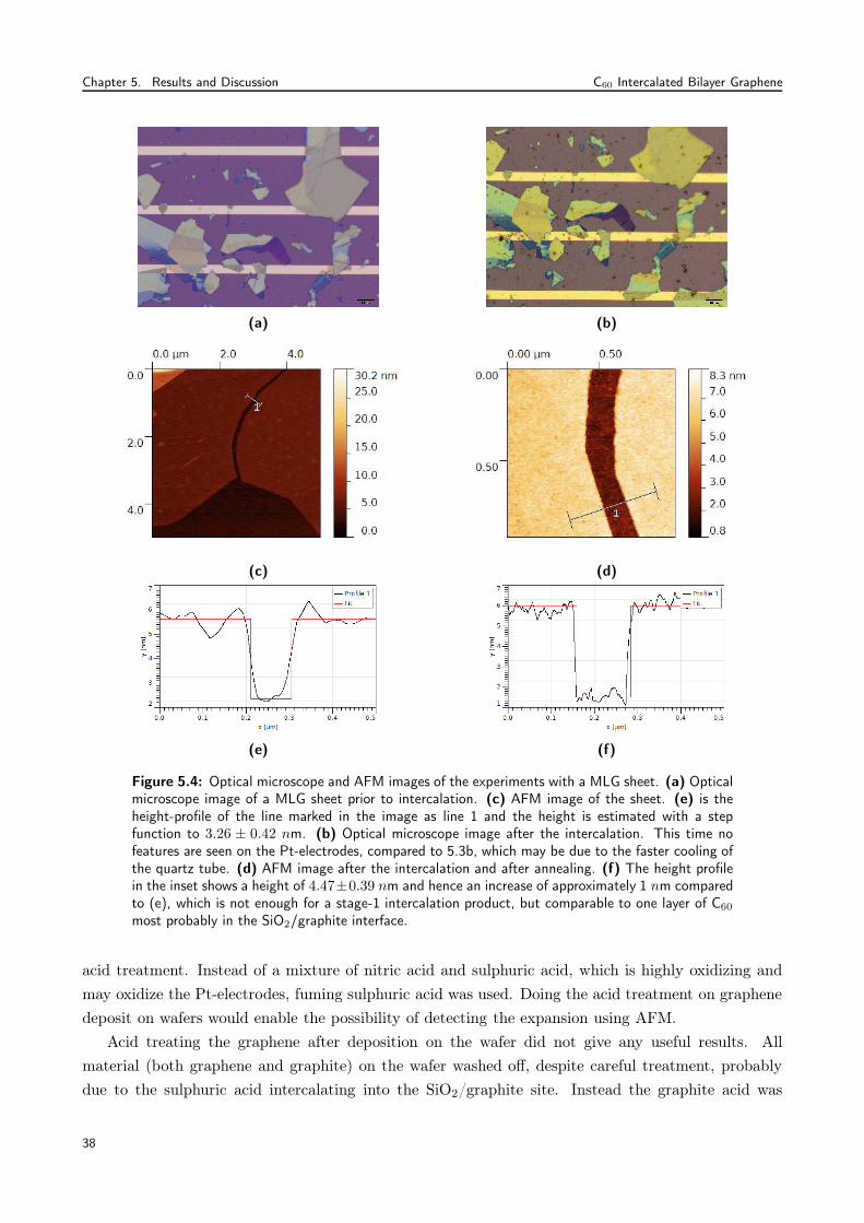
Chapter 5. Results and Discussion C60 Intercalated Bilayer Graphene
(a) (b)
(c) (d)
(e) (f)
Figure 5.4: Optical microscope and AFM images of the experiments with a MLG sheet. (a) Opticalmicroscope image of a MLG sheet prior to intercalation. (c) AFM image of the sheet. (e) is theheight-profile of the line marked in the image as line 1 and the height is estimated with a stepfunction to 3.26 ± 0.42 nm. (b) Optical microscope image after the intercalation. This time nofeatures are seen on the Pt-electrodes, compared to 5.3b, which may be due to the faster cooling ofthe quartz tube. (d) AFM image after the intercalation and after annealing. (f) The height profilein the inset shows a height of 4.47±0.39 nm and hence an increase of approximately 1 nm comparedto (e), which is not enough for a stage-1 intercalation product, but comparable to one layer of C60
most probably in the SiO2/graphite interface.
acid treatment. Instead of a mixture of nitric acid and sulphuric acid, which is highly oxidizing and
may oxidize the Pt-electrodes, fuming sulphuric acid was used. Doing the acid treatment on graphene
deposit on wafers would enable the possibility of detecting the expansion using AFM.
Acid treating the graphene after deposition on the wafer did not give any useful results. All
material (both graphene and graphite) on the wafer washed off, despite careful treatment, probably
due to the sulphuric acid intercalating into the SiO2/graphite site. Instead the graphite acid was
38

C60 Intercalated Bilayer Graphene Chapter 5. Results and Discussion
treated pre-deposition. The first indication of successful absorption of the acid into the inter-planar
sites, could be seen from the weight of the graphite, which approximately double for all graphite pieces,
independent on the initial weight of the graphite pieces.
A combination of SEM and XRD measurements, were used in order to verify that the graphite have
preserved the high order and quality after the acid treatment. Figure 5.5 is SEM images of pristine
and acid treated graphite, 5.5a and 5.5b respectively. The highly planar structure of the pristine
graphite, has been visualized by showing an edge where the layered structure is visible. The acid
treated graphite shows the same structure indicating preservation of the same highly planar structure.
The layered structure seen here is not single layers of graphene thus the interlayer distance can not
be extracted from these images, as the scale is to large. The two images look slightly different, with
the planar lines in the acid treated more separated. This is however due to variations in the specific
sample, and do not indicate a change in the sample after acid treatment. At least not on a scale of
100 nm.
(a) (b)
Figure 5.5: SEM image of (a) Pristine graphite (b) Acid treated graphite. Both images shows thelayered structure of graphite, indicating that the acid treatment does not destroy the planar order.
XRD experiments were conducted to give information on small changes to the interlayer distance
after acid treating the gaphite. The data presented in figure 5.6 are taken with a XRD apparatus
at Risø, DTU, with x-ray wavelength λ = 1.54 Å, hence the peak position values extracted from the
fits have at most a precision to the second decimal due to the limitation from the x-ray wavelength
distribution, see section 4.4 for discussion on the uncertainties of the measurements. Figure 5.6a
shows the high quality of the graphite, also seen in the SEM images. The spectrum only show two
very sharp peaks, namely one at 26.64 ± 0.01 and 54.75 ± 0.01. The first correspond to a very well-
defined reflection from the (002)-plane, and gives an interlayer distance of 3.34 Å. The second peak at
54.75 ± 0.01, corresponding to d = 1.670 Å, for n = 1, but is most probably the second order peak of
the (002)-reflection, see section 4.6. After the acid treatment a slight decrease in the position of the
(002)-peak at 25.30 ± 0.01, resulting in an increased in d spacing for the (002) direction, d = 3.52
Å, see figure 5.6b. Furthermore the peak is more broaden (going from a FWHM of 0.08 ± 0.01 to
0.70 ± 0.03), assigned to a less well-defined d-spacing. Again is the second order peak to the (002)-
39

Chapter 5. Results and Discussion C60 Intercalated Bilayer Graphene
reflection visible, namely at 51.89 ± 0.2. The two new peaks at 29.67 ± 0.09 and 56.65 ± 0.1
corresponds to a diffraction plane distance of 3.01 Å and 1.62 Å, respectively. The specific origin of
these peaks are still unknown.
The increased d-spacing after acid treatment most likely was due to intercalation of the sulphuric
acid. Which would also explain the broadening of the (002)-peak as the arrangement of the intercala-
tion molecules would not be as perfect as the pristine graphite layers. But the (002)-direction is still
preserved enough for the second order peak to be visible, indicating that the highly ordered structure
is preserved, only with a slight different plane distance. An explanation of the two new peaks could
be due to an in-plane periodic arrangement of the intercalated molecules, giving rise to lattice plane
diffraction, or due to a constant distance between intercalated molecules between graphene layers.
Instead of using a acid mixture of nitric and sulphuric acid as proposed by Chen et al. 13 , the XRD
data indicates that a pure sulphuric acid treatment is enough to produce expanded graphite. This is
concluded as it seem very likely that the observed change in diffraction pattern can be contributed to
successful intercalation. XRD measurements on the expanded graphite, obtained by heat treating the
acid treated graphite, are presented in section 5.3.
10 20 30 40 50 60 70 800
200000
400000
600000
800000
1000000
1200000
1400000
Inte
nsity
[a.u
.]
2
Pristine Graphite Lorentz Fit to peak at 26.64 Lorentz Fit to peak at 54.75 Cumulative Fit Peak
(a)
10 20 30 40 50 60 70 80
0
100000
200000
300000
400000
500000
Inte
nsity
[a.u
.]
2
Acid Treated Graphite Lorentz Fit to Peak at 25.30 Lorentz Fit to Peak at 29.67 Lorentz Fit to Peak at 51.89 Lorentz Fit to Peak at 56.65 Cumulative Fit Peak
(b)
Figure 5.6: XRD measurements on graphite. Lorentz functions are used for peak fitting. (a)Pristine graphite, with two pronounced peaks, one at 26.64 originating from the (002)-reflectionand the second order of this at 54.75, corresponding to a interlayer distance of 3.34 Å. (b) Acidtreated graphite, which shows a quit different spectrum. The (002)-reflection is moved to 25.30,with second order at 51.89 and d-spacing of d = 3.52 Å.
Due to limited time, experiments with C60 intercalation into expanded graphite on SiO2-wafer
were not conducted. Instead it was attempted to intercalate C60 into bulk graphite, and then wafer
deposit afterwards.
5.3 Graphite Intercalated Compounds
After intercalation attempt, but before wafer-deposition, XRD measurements were conducted, on both
expanded graphite and the attempted C60 graphite intercalated compound (GIC), see figure 5.7. The
expanded graphite was produced by heat treating the acid treated graphite. The GIC was produced
from expanded graphite. The two spectra, taken at MaxLab with an x-ray wavelength of λ = 1.048
40
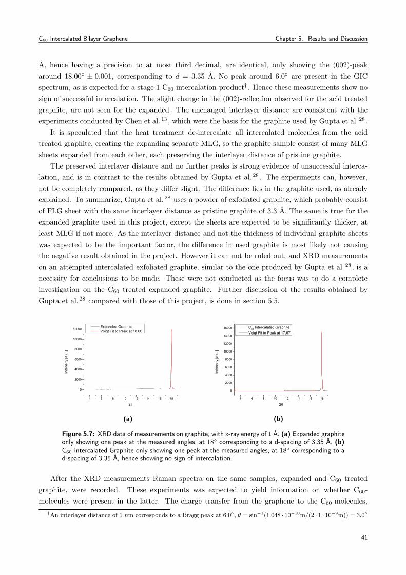
C60 Intercalated Bilayer Graphene Chapter 5. Results and Discussion
Å, hence having a precision to at most third decimal, are identical, only showing the (002)-peak
around 18.00 ± 0.001, corresponding to d = 3.35 Å. No peak around 6.0 are present in the GIC
spectrum, as is expected for a stage-1 C60 intercalation product†. Hence these measurements show no
sign of successful intercalation. The slight change in the (002)-reflection observed for the acid treated
graphite, are not seen for the expanded. The unchanged interlayer distance are consistent with the
experiments conducted by Chen et al. 13 , which were the basis for the graphite used by Gupta et al. 28 .
It is speculated that the heat treatment de-intercalate all intercalated molecules from the acid
treated graphite, creating the expanding separate MLG, so the graphite sample consist of many MLG
sheets expanded from each other, each preserving the interlayer distance of pristine graphite.
The preserved interlayer distance and no further peaks is strong evidence of unsuccessful interca-
lation, and is in contrast to the results obtained by Gupta et al. 28 . The experiments can, however,
not be completely compared, as they differ slight. The difference lies in the graphite used, as already
explained. To summarize, Gupta et al. 28 uses a powder of exfoliated graphite, which probably consist
of FLG sheet with the same interlayer distance as pristine graphite of 3.3 Å. The same is true for the
expanded graphite used in this project, except the sheets are expected to be significantly thicker, at
least MLG if not more. As the interlayer distance and not the thickness of individual graphite sheets
was expected to be the important factor, the difference in used graphite is most likely not causing
the negative result obtained in the project. However it can not be ruled out, and XRD measurements
on an attempted intercalated exfoliated graphite, similar to the one produced by Gupta et al. 28 , is a
necessity for conclusions to be made. These were not conducted as the focus was to do a complete
investigation on the C60 treated expanded graphite. Further discussion of the results obtained by
Gupta et al. 28 compared with those of this project, is done in section 5.5.
4 6 8 10 12 14 16 18
0
2000
4000
6000
8000
10000
12000
Inte
nsity
[a.u
.]
2
Expanded Graphite Voigt Fit to Peak at 18.00
(a)
4 6 8 10 12 14 16 18
0
2000
4000
6000
8000
10000
12000
14000
16000
Inte
nsity
[a.u
.]
2
C60 Intercalated Graphite Voigt Fit to Peak at 17.97
(b)
Figure 5.7: XRD data of measurements on graphite, with x-ray energy of 1 Å. (a) Expanded graphiteonly showing one peak at the measured angles, at 18 corresponding to a d-spacing of 3.35 Å. (b)C60 intercalated Graphite only showing one peak at the measured angles, at 18 corresponding to ad-spacing of 3.35 Å, hence showing no sign of intercalation.
After the XRD measurements Raman spectra on the same samples, expanded and C60 treated
graphite, were recorded. These experiments was expected to yield information on whether C60-
molecules were present in the latter. The charge transfer from the graphene to the C60-molecules,
†An interlayer distance of 1 nm corresponds to a Bragg peak at 6.0, θ = sin−1(1.048 · 10−10m/(2 · 1 · 10−9m)) = 3.0
41

Chapter 5. Results and Discussion C60 Intercalated Bilayer Graphene
should move the graphene G peak towards higher wave-numbers. The G-peak position differs slightly
between the two samples, with the position for expanded graphite around 1589.6 cm−1±0.6 and 1591.8
cm−1 ± 0.6 for the intercalated. The observed difference, albeit small, might be due to a p-doping of
the graphite from the C60. If a C60-molecule film did cover the graphite sample, the ratio of doped
graphene sheets to pristine sheets (not in direct contact to C60) might be high enough to be detected
in the measurement. Raman data of a proposed stage-4 compound of the C60-intercalation graphite,
is reported to yield a double peak, as the G peak splits for the doped and undoped layers of the
sample29. Unfortunately such a splitting might not be detectable in the spectrum in figure 5.8b as the
spectrum unfortunately was taken with a too low resolution, hence the expected difference between
the G peak position of a C60 doped and pristine graphene would possibly lie within the resolution of
the spectra which was 5 cm−1 per measuring point, see section 2.4. If this is the case a double peak
might be measured as single peak if both peak maxima is within the same measuring interval, giving
a peak position between the to original peaks. New and higher resolution measurements are desirable,
but due to reconstruction of the laboratory the Raman spectrometer was inoperative at the time the
mistake was detected.
A more thorough discussion of the results obtained compared to Gupta et al. 28 is conducted in
section 5.5.
1500 2000 2500 3000 3500
0
500
1000
1500
2000
2500
Ram
an In
tens
ity
Raman Shift [cm-1
Expanded Graphite Voigt Fit to G-peak at 1590 cm-1
(a)
1500 2000 2500 3000 3500
0
200
400
600
800
1000
1200
1400
1600
1800
Ram
an In
tens
ity
Raman Shift [cm-1]
C60 Intercalated Graphite
Voigt Fit to G-peak at 1592 cm-1
(b)
Figure 5.8: Raman spectra taken with a laser wavelength of λ = 514 nm. (a) Expanded graphite(b) Intercalated graphite
As the original goal was to do transport measurements on C60 intercalated BLG with use of
CAFM, wafers with FLG sheets were prepared from three different types of graphite, namely pristine,
expanded graphite and "intercalated" graphite. These measurements were conducted despite the
negative results from above presented experiments, but it might be possible to detect a difference in
conductance between pristine and expanded graphite.
I-V curves were recorded with CAFM at four different sites for two FLG sheet prepared from the
pristine graphite, referred to as P1 and P2, see figure 5.9 and B.4, respectively. By direct comparing
the I-V curves for P1 it can be seen that the conductance is stable for three of the four measurements,
namely for the two at the electrode (place 1 and 4) and for the sheet close to the electrode (place 2).
The measurements away from the electrode shows an slight decrease in slope, e.i. in conductance. At
first glance this could be due to the increased distance to the sheet, but are more likely bad contact
42

C60 Intercalated Bilayer Graphene Chapter 5. Results and Discussion
between the tip and the flake as will be discussed below. However a series of measurements on the
sheet with increasing distance to the electrode might reveal whether of the two are a valid explanation.
The measured conductances, for both P1 and P2, are summarized in table 5.1.
Place1 - Electrode Place2 - Sheet Place3 - Sheet Place4 - Electrode Linear Fit to Place 1 Linear Fit to Place 2 Linear Fit to Place 3 Linear Fit to Place 4
-0.004 -0.002 0.000 0.002 0.004
-2.00E-009
-1.50E-009
-1.00E-009
-5.00E-010
0.00E+000
5.00E-010
1.00E-009
1.50E-009
2.00E-009
Cur
rent
[A]
Voltage [V]
(a)
+1,4
+2 +3
(b)
Figure 5.9: Conducting AFM on a pristine few-layered graphene flake deposited on SiO2, referredto as flake 1. (a) Conducting AFM measurements of pristine few layered graphene sheet, first at theelectrode then twice at the sheet and lastly at the electrode again, see (b) for specific places. Theconductances are extracted by a linear fit to the data. (b) AFM image of flake 1. The measuringsites are marked by a +-sign and a number. Inset are the line profile 1, and the fitted square profileyields a sheet height of 4.9 nm.
Place 1 and 4 are direct measurements on the electrode, before and after engaging the flake,
verifying whether the contact between the CAFM tip and the sample changed with the number of
measurements. Comparing the two measurements for P1, 2.72 MΩ and 2.76 MΩ, no change are
observe as the slight different are within the uncertainty of the measurements. Indication on some
degradation of the tip for P2, are visualized by resistance increasing from 2.60 MΩ to 2.84 MΩ, see
figure B.4 for the I-V curves. The two measurements on P2 (place 2 and 3) shows a general degradation
after engaging the sample, with place 3 having the same total resistance as the second measurement
on the electrode (place 4).
From the measurements on pristine graphite samples, a tendency towards the resistance of the
pristine graphite sheet being too low to alter the total resistance detectable, is observed. Furthermore
it is seen that resistances between 2.6 MΩ and 3.1 MΩ are the interval of expectable values for
this type of device, taking degradation of the tip and the slightly random tip-sample resistance into
account. Hence the good statistics on the every individual I-V curve, as discussed in section 4.3, is
irrelevant as the total resistant of the system can change from 2.55 MΩ to 2.84 MΩ for the same place
on the same electrode. Thus a graphite sheet resistance of the order of MΩ might be necessary to
be detectable. This rather unstable measurements makes the technique less suitable for these highly
conductive samples.
The CAFM measurements on two flakes of C60 intercalated graphite, referred to as I1 and I2,
can be seen in figure 5.10 and B.5. Again are the differences between measurements directly on the
electrodes and on the flake not pronounced. Comparing the I-V curves for pristine graphite, figure 5.9,
and the intercalated sample, 5.10, only supports the Raman and XRD measurements in showing no
43
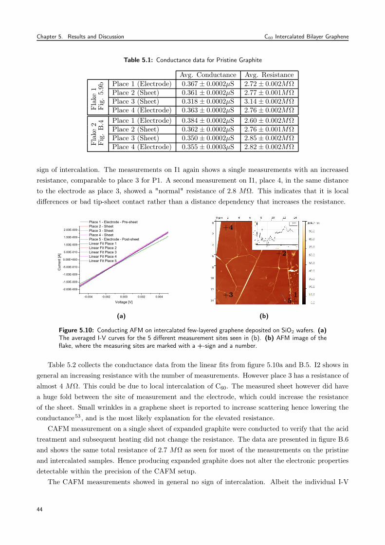
Chapter 5. Results and Discussion C60 Intercalated Bilayer Graphene
Table 5.1: Conductance data for Pristine Graphite
Avg. Conductance Avg. Resistance
Fla
ke1
Fig
.5.
9b Place 1 (Electrode) 0.367 ± 0.0002µS 2.72± 0.002MΩPlace 2 (Sheet) 0.361 ± 0.0002µS 2.77± 0.001MΩPlace 3 (Sheet) 0.318 ± 0.0002µS 3.14± 0.002MΩPlace 4 (Electrode) 0.363 ± 0.0002µS 2.76± 0.002MΩ
Fla
ke2
Fig
.B
.4 Place 1 (Electrode) 0.384 ± 0.0002µS 2.60± 0.002MΩPlace 2 (Sheet) 0.362 ± 0.0002µS 2.76± 0.001MΩPlace 3 (Sheet) 0.350 ± 0.0002µS 2.85± 0.002MΩPlace 4 (Electrode) 0.355 ± 0.0003µS 2.82± 0.002MΩ
sign of intercalation. The measurements on I1 again shows a single measurements with an increased
resistance, comparable to place 3 for P1. A second measurement on I1, place 4, in the same distance
to the electrode as place 3, showed a "normal" resistance of 2.8 MΩ. This indicates that it is local
differences or bad tip-sheet contact rather than a distance dependency that increases the resistance.
Place 1 - Electrode - Pre-sheet Place 2 - Sheet Place 3 - Sheet Place 4 - Sheet Place 5 - Electrode - Post-sheet Linear Fit Place 1 Linear Fit Place 2 Linear Fit Place 3 Linear Fit Place 4 Linear Fit Place 5
-0.004 -0.002 0.000 0.002 0.004
-2.00E-009
-1.50E-009
-1.00E-009
-5.00E-010
0.00E+000
5.00E-010
1.00E-009
1.50E-009
2.00E-009
Cur
rent
[A]
Voltage [V]
(a)
15+
+2
+3
+4
(b)
Figure 5.10: Conducting AFM on intercalated few-layered graphene deposited on SiO2 wafers. (a)The averaged I-V curves for the 5 different measurement sites seen in (b). (b) AFM image of theflake, where the measuring sites are marked with a +-sign and a number.
Table 5.2 collects the conductance data from the linear fits from figure 5.10a and B.5. I2 shows in
general an increasing resistance with the number of measurements. However place 3 has a resistance of
almost 4 MΩ. This could be due to local intercalation of C60. The measured sheet however did have
a huge fold between the site of measurement and the electrode, which could increase the resistance
of the sheet. Small wrinkles in a graphene sheet is reported to increase scattering hence lowering the
conductance53 , and is the most likely explanation for the elevated resistance.
CAFM measurement on a single sheet of expanded graphite were conducted to verify that the acid
treatment and subsequent heating did not change the resistance. The data are presented in figure B.6
and shows the same total resistance of 2.7 MΩ as seen for most of the measurements on the pristine
and intercalated samples. Hence producing expanded graphite does not alter the electronic properties
detectable within the precision of the CAFM setup.
The CAFM measurements showed in general no sign of intercalation. Albeit the individual I-V
44

C60 Intercalated Bilayer Graphene Chapter 5. Results and Discussion
Table 5.2: Conductance data for Intercalated Graphite
Avg. Conductance Avg. Resistance
Fla
ke1
Fig
.5.
10b Place 1 (Electrode) 0.369µS 2.71MΩ
Place 2 (Sheet) 0.360µS 2.78MΩPlace 3 (Sheet) 0.320µS 3.12MΩPlace 4 (Sheet) 0.359µS 2.79MΩPlace 5 (Electrode) 0.364µS 2.74MΩ
Fla
ke2
Fig
.B
.5 Place 1 (Electrode) 0.373µS 2.68MΩPlace 2 (Sheet) 0.347µS 2.87MΩPlace 3 (Sheet) 0.251µS 3.99MΩPlace 4 (Electrode) 0.327µS 3.06MΩ
curves was recorded with many measuring points, hence increasing the statistics, random tip-sample
contacts neutralized this, giving measured resistance varying 0.3 MΩ for two individual measurements
on the same sample same place.
To summarize the experiments on synthesis of a pure C60 intercalated graphite compound, non
of the results gives indications towards that the intercalation were successful. A higher resolution
Raman spectrum, would give information on whether the graphite where doped by the C60, but it
could be speculated that for a highly expanded (or exfoliated) graphite sample the surface adsorbed
C60-molecules could yield the same result as an intercalation product. Further discussion can be found
in section 5.5.
5.4 Potassium and C60 co-Intercalated Bilayer Graphene
Another approach towards intercalation of C60-molecules into bilayer graphene was attempted, thro-
ugh an intermediate product of potassium intercalated graphite. Both solution-based, inspired by the
work of Fuhrer et al. 23 , and thermal intercalation experiments were conducted. As most of the samples
from these experiments were very unstable in the atmosphere, proper characterization were difficult
and hence all discussions are based on optical microscope images, limiting the conclusive statements.
5.4.1 Pre-cursor C8K
The pre-cursor, stage-1 potassium intercalated graphite C8K, was prepared by thermal intercalation.
Characterization of this GIC is limited as the potassium covering the sample oxidized and destroyed
the samples. Figure 5.12a are an optical microscope image of a sample after intercalation of potassium
still inside the quartz tube, hence the blurry image. For a image of a sample exposed to the air after the
quartz tube were smashed see figure 5.11. The apparent wet surface is probably due to the potassium
reacting with the oxygen or water in the air forming either potassium oxide or hydroxide (probably
both). The surface of the wafer could due to the fast oxidation not be further investigated, but from
analysis of the optical microscope images (both 5.12a and 5.11b), it seems likely that a potassium film
did cover the entire wafer. The change in contrast of the graphite sheets indicate that the potassium
intercalation was successful, but this is very speculative.
45

Chapter 5. Results and Discussion C60 Intercalated Bilayer Graphene
(a) (b)
Figure 5.11: Optical microscope images of the potassium intercalated graphite samples on wafersexposed to the air. (a) Overview of such a sample. (b) Zoom of graphite sheets, which in this imagehas a gold contrast. The contrast could indicate potassium intercalation, albeit it is hard to deduceanything from these colourful images.
The potassium film covering the wafer was tried removed by creating a temperature gradient
through the quartz tube, with the wafer at the high temperature end. The hope was that it required
more energy to remove the intercalated potassium than that on the surface. Figure 5.12b is the wafer
after 35 min at 100C. Comparing figure 5.12a and 5.12b, the same contrast between the SiO2- and
Pt-areas are seen. On the contrary some of the graphite sheets have changed color. This indicates
de-intercalation of potassium rather than desorption from the surface. These observations, however
are very speculative and more experiments needs to be conducted before anything can be said. These
experiments could be a more thorough determination of the temperature dependence of the desorption
of potassium. Raman measurements could be used to determine if the potassium was intercalated and
if it did deintercalated under the heat treatment. This would be evident from the doping dependency
of the G-peak position. Also an appropriate way of handling the potassium samples are needed,
which not only should protect against the oxidization, but also hold the possibility of conducting
characterization measurements in situ.
5.4.2 Solution Based Intercalation
After potassium intercalation, C60-molecules were tried intercalated through solution. The result can
be seen in figure 5.13a, which is an optical microscope image of the same area as in 5.12 (just rotated
90). From this it evident that something had happen, but it is still unknown whether the intercalation
was successful or not. A likely scenario is that the suggested potassium film, had been intercalated
with a combination of C60 and benzene, as an intercalation product of potassium and C60 are well
documented in the literature88. A Raman measurement would give further indications towards what
reaction had taken place.
The results showed that this type of reaction are either not suited for samples on wafers or a lot of
optimization are needed. Figure 5.13b shows another part of the sample, where the bottom electrodes
have been destroyed. The observation that the electrodes seems flushed away, could indicates that
46
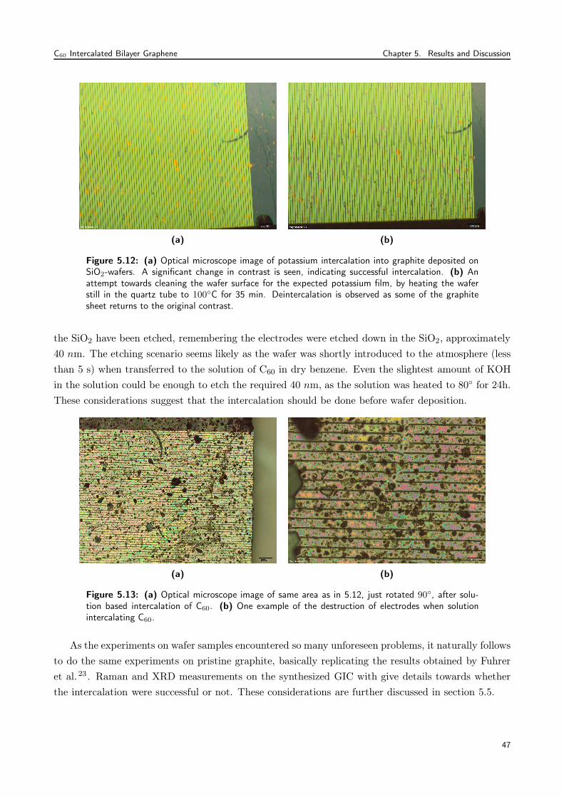
C60 Intercalated Bilayer Graphene Chapter 5. Results and Discussion
(a) (b)
Figure 5.12: (a) Optical microscope image of potassium intercalation into graphite deposited onSiO2-wafers. A significant change in contrast is seen, indicating successful intercalation. (b) Anattempt towards cleaning the wafer surface for the expected potassium film, by heating the waferstill in the quartz tube to 100C for 35 min. Deintercalation is observed as some of the graphitesheet returns to the original contrast.
the SiO2 have been etched, remembering the electrodes were etched down in the SiO2, approximately
40 nm. The etching scenario seems likely as the wafer was shortly introduced to the atmosphere (less
than 5 s) when transferred to the solution of C60 in dry benzene. Even the slightest amount of KOH
in the solution could be enough to etch the required 40 nm, as the solution was heated to 80 for 24h.
These considerations suggest that the intercalation should be done before wafer deposition.
(a) (b)
Figure 5.13: (a) Optical microscope image of same area as in 5.12, just rotated 90, after solu-tion based intercalation of C60. (b) One example of the destruction of electrodes when solutionintercalating C60.
As the experiments on wafer samples encountered so many unforeseen problems, it naturally follows
to do the same experiments on pristine graphite, basically replicating the results obtained by Fuhrer
et al. 23 . Raman and XRD measurements on the synthesized GIC with give details towards whether
the intercalation were successful or not. These considerations are further discussed in section 5.5.
47
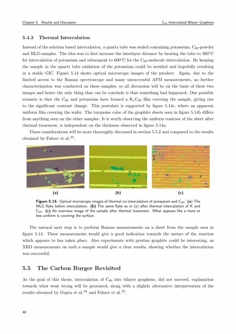
Chapter 5. Results and Discussion C60 Intercalated Bilayer Graphene
5.4.3 Thermal Intercalation
Instead of the solution based intercalation, a quartz tube was sealed containing potassium, C60-powder
and BLG-samples. The idea was to first increase the interlayer distance by heating the tube to 300C
for intercalation of potassium and subsequent to 600C for the C60-molecule intercalation. By keeping
the sample in the quartz tube oxidation of the potassium could be avoided and hopefully resulting
in a stable GIC. Figure 5.14 shows optical microscope images of the product. Again, due to the
limited access to the Raman spectroscope and many unsuccessful AFM measurements, no further
characterization was conducted on these samples, so all discussion will be on the basis of these two
images and hence the only thing that can be conclude is that something had happened. One possible
scenario is that the C60 and potassium have formed a KxC60 film covering the sample, giving rise
to the significant contrast change. This postulate is supported by figure 5.14c, where an apparent
uniform film covering the wafer. The turquoise color of the graphite sheets seen in figure 5.14b differs
from anything seen on the other samples. It is worth observing the uniform contrast of the sheet after
thermal treatment, is independent on the thickness observed in figure 5.14a.
These considerations will be more thoroughly discussed in section 5.5.2 and compared to the results
obtained by Fuhrer et al. 23 .
(a) (b) (c)
Figure 5.14: Optical microscope images of thermal co-intercalation of potassium and C60. (a) TheMLG flake before intercalation. (b) The same flake as in (a) after thermal intercalation of K andC60. (c) An overview image of the sample after thermal treatment. What appears like a more orless uniform is covering the surface.
The natural next step is to perform Raman measurements on a sheet from the sample seen in
figure 5.14. These measurements would give a good indication towards the nature of the reaction
which appears to has taken place. Also experiments with pristine graphite could be interesting, as
XRD measurements on such a sample would give a clear results, showing whether the intercalation
was successful.
5.5 The Carbon Burger Revisited
As the goal of this thesis, intercalation of C60 into bilayer graphene, did not succeed, explanation
towards what went wrong will be presented, along with a slightly alternative interpretation of the
results obtained by Gupta et al. 28 and Fuhrer et al. 23 .
48

C60 Intercalated Bilayer Graphene Chapter 5. Results and Discussion
5.5.1 C60 Intercalated Bilayer Graphene
The main goal, synthesizing a pure carbon structure by thermally intercalating C60-molecules into
BLG or graphite were unsuccessful, albeit Gupta et al. 28 have demonstrated the intercalation into
graphite. As discussed in chapter 2 they verify the structure with use of Raman spectroscopy and
TEM imagining and diffraction.
The Raman data shows a doping of the G-peak indicating charge transfer from graphene to the
C60, changing their Fermi-levels. This doping is as such not evidence for successful intercalation as
a C60 covered graphene sheet would give a similar result. Albeit one would expect a double peak
from C60 covered graphite, the type of graphite used by Gupta et al. 28 , i.e. highly exfoliated graphite
powder with a high percentage of FLG sheets13, could probably yield the published results. In another
article by Gupta et al. 29 from 2005, they publish Raman data from both stage-1 and stage-4 GICs,
see figure 5.15. The stage-1 compound is the same as discussed before, but the stage-4 shows some
different characteristics. The G-peak is split into two individual peaks, one at 1582 cm−1 and another
at 1586.6 cm−1, assigned to a pristine and an up-shifted E2g-mode of graphite, respectively. The
splitting is assigned to the difference between layers in contact with intercalated species and those not
in contact. Hence they argue that stage-1 should be a single peak, as seen from figure 5.15a, while
for stages ≥ 2 a double peak would appear, as seen in 5.15b. It is not given that a stage-2 compound
would yield a double peak as every graphene sheet in this compound are in direct contact to a C60
layer. For stage ≥ 3 it seems more likely that the graphene can screen doping from the layer not in
direct contact with the C60-molecules, which might preserve the original E2g-mode.
(a) (b)
Figure 5.15: Raman spectra of (a) stage-1 and (b) stage-4 compound of C60 intercalated. Adoptedfrom Gupta et al. 29
In the article from Gupta et al. 29 they also show the TEM data from both a stage-1 and stage-4
compound, figure 5.16a and 5.16b respectively. From the images Gupta et al. 29 find a interlayer
distance of 1.27 nm for the stage-1 compound, but does not extract the distance for the stage-4
compound. In the article from 200428 they include a diffraction image from a sample similar to the
one seen on figure 5.16a. They comment that the sample showed hexagonal symmetry, but apart from
that the diffraction pattern is not further used. For a stage-1 compound the distance between two
49
Chapter 5. Results and Discussion C60 Intercalated Bilayer Graphene
C60 monolayers is expected to be approximately 1.3 nm. The distance between C60-molecules in a
monolayer is approximately 1 nm16. In the lower left corner of figure 5.16a is a rough hand-drawn
hexagon to indicate the hexagonal nature of the sample. The distances between opposite corners
in this non-precise drawing are 3.05 nm, 2.93 nm and 2.9 nm, approximately yielding a C60-C60
distance of 1.5 nm, surprisingly independent whether they are separated by a graphene layer or not.
This is supported by the diffraction image seen in 5.16c, where 5.16d is an enlargement of the lowest
order diffraction peaks. Again a hexagon is hand-drawn to visualize the hexagonal structure and to
show the points between which the distance was measured. As the original image did not include
information on the scale, one of the opposite corner distances was set to 1. By coincident the other
two distances did also hit 1, with two decimals precision, giving further indications towards an equally
sided hexagonal lattice. Such a lattice could indicate that the measured TEM and diffraction data
might be a monolayer of C60 molecules on a FLG sheet. However the measured NN distance for the
C60-molecules of 1.5 nm larger than the 1 nm expected within the monolayer, is not in agreement
whit this statement. A diffraction pattern from the presumed stage-4 compound would have helped
describing the overall structure for the GICs. Thus the stage-4 compound can not be further discussed.
Although XRD measurements on C60 intercalated expanded graphite did not indicate intercalation,
these measurements can not be used when attempting to deduce whether the data presented by Gupta
et al. 28 show intercalated graphite or graphite covered by C60-molecules. The reason for this is the
difference in the graphite used. As mentioned before the graphite was processed within the terms
of Chen et al. 13 . The interlayer distance was expected to be the important factor. Chen et al. 13
show that both the graphite nano-sheet and the graphite worms retain the same interlayer distance
as pristine graphite. Hence it was decided to do the intercalation experiments with nano-sheets, even
though Gupta et al. 28 most probably used the graphite worms. The graphite worms, which were
exfoliated expanded graphite, is a powder consisting of many FLG sheets. Depending on the efficiency
of the exfoliation, parts of such a sample might yield the Raman data seen for both presumed stage-
1 and stage-4 compounds after intercalation. If it is presumed that the TEM data for the stage-1
compound instead shows a C60 film covering a FLG sheet, this could also be a possible scenario with
the graphite worms. Although the found C60-C60 distance is inconsistent with this explanation, it is
also difficult to describe within the intercalation scenario, as equal distances would not be expected.
A difference in distance between C60 molecules separated by a graphene layer and in direct contact is
expected.
5.5.2 Potassium and C60 co-Intercalated Bilayer Graphene
The experiments with co-intercalation of potassium and C60-molecules were inspired by the work done
by Fuhrer et al. 23 . As discussed previously they state to have synthesized the heterostructure with
the stoichiometry C32K4C60. This postulate is only backed-up by transport measurements, showing
superconductivity of the sample with Tc = 19.5C. Raman spectroscopy and XRD measurements were
at the time of publication (1994) ongoing, but have unfortunately never been published. Also the Tc’s
dependency on the electric and magnetic field were in progress, but for some reason remained un-
published. If published these measurements would clearly demonstrate whether the superconductivity
50
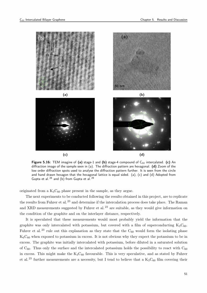
C60 Intercalated Bilayer Graphene Chapter 5. Results and Discussion
(a) (b)
(c) (d)
Figure 5.16: TEM imagine of (a) stage-1 and (b) stage-4 compound of C60 intercalated. (c) Andiffraction image of the sample seen in (a). The diffraction pattern are hexagonal. (d) Zoom of thelow order diffraction spots used to analyse the diffraction pattern further. It is seen from the circleand hand drawn hexagon that the hexagonal lattice is equal sided. (a), (c) and (d) Adopted fromGupta et al. 28 and (b) from Gupta et al. 29
originated from a K3C60 phase present in the sample, as they argue.
The next experiments to be conducted following the results obtained in this project, are to replicate
the results from Fuhrer et al. 23 and determine if the intercalation process does take place. The Raman
and XRD measurements suggested by Fuhrer et al. 23 are suitable, as they would give information on
the condition of the graphite and on the interlayer distance, respectively.
It is speculated that these measurements would most probably yield the information that the
graphite was only intercalated with potassium, but covered with a film of superconducting K3C60.
Fuhrer et al. 23 rule out this explanation as they state that the C60 would form the isolating phase
K6C60 when exposed to potassium in excess. It is not obvious why they expect the potassium to be in
excess. The graphite was initially intercalated with potassium, before diluted in a saturated solution
of C60. Thus only the surface and the intercalated potassium holds the possibility to react with C60
in excess. This might make the K3C60 favourable. This is very speculative, and as stated by Fuhrer
et al. 23 further measurements are a necessity, but I tend to believe that a K3C60 film covering their
51

Chapter 5. Results and Discussion C60 Intercalated Bilayer Graphene
graphite was the origin of the measured superconductivity and transition temperature of 19.5 K
Furthermore, the possibly large amount of potassium adsorbing to the surface have been reduced
by the two-zone intercalation technique used by Fuhrer et al. 23 , compared to what was observed for
the measurements in this project. A thermal gradient between the potassium and the graphite should
minimize the adsorption17 , albeit a thin potassium film would still be expected to cover the graphite.
This might have helped in the experiments on wafers, but is not expected to have solved the problem
totally, as the removal of the expected potassium film proved very hard. Thus it is still believed that
these experiments are not suitable for wafer-samples.
52
Chapter 6
Conclusion and Outlook
The main aim of this project was to synthesize a 2D all-carbon heterostructure consisting of a C60
monolayer between two graphene electrodes. The structure was attempted produced by fabrication of
bilayer graphene samples on bottom electrodes, followed by thermal intercalation of C60-molecules, as
proposed by Gupta et al. 28 . The structural characterization was done with an optical microscope, an
atomic force microscope, a scanning electron microscope, a Raman spectrometer and x-ray diffraction
measurements. Electrical characterization was conducted with a conducting atomic force microscope.
None of these indicated successful production of the structure.
The second part of the project was to intercalate C60 into graphite. The same characterization
techniques as in the first part did not show any signs of intercalation for these samples either.
The last part was to expand the interlayer distance of bilayer graphene by intercalation of potas-
sium into graphite, potentially easing the intercalation of C60 molecules. These samples were only
characterized with optical microscopy, hence all conclusions stated from this part are very speculative.
The results from the three different parts of the project, albeit mostly negative, will be concluded
and suggestions to future work will be given within each of these. Finally some overall conclusive
remarks are given, to wrap up the project at the final year of my education.
6.1 C60 Intercalated Bilayer Graphene
The main objective of the thesis was to intercalate BLG with a monolayer of C60 molecules and
conduct structural and electrical characterization of the compound. The structural and electrical
characterization was successfully conducted, unfortunately not showing any sign of intercalation.
The initial structural characterization measurements were done with AFM, which was the main
technique for characterization of graphene samples deposited on wafers. All samples produced, both
FLG and MLG, showed no significant increase in sheet thickness as proposed both theoretically75 and
experimentally28 for a stage-1 intercalation compound.
The small interlayer distance is thought to be the main hindering for the successful intercalation
of C60 molecules, hence the graphite interlayer distance was attempted increased. This was done by
treating the graphite with oleum followed by heat treatment, inspired by the work of Chen et al. 13 . It
proved impossible to do the acid treatment or deposition of acid treated graphite on wafers. It would
53

Chapter 6. Conclusion and Outlook C60 Intercalated Bilayer Graphene
be possible to deposit expanded graphite on Si wafers and do the intercalation experiments on these.
These experiments would most likely yield the same unsuccessful results as for the expanded graphite,
reviewed below. Hence further experiments on wafers should first be conducted, when successful
intercalation into some type of graphite has been demonstrated, it being expanded, exfoliated or a
third new type.
6.2 C60 Intercalated Graphite Compounds
The prepared expanded graphite, expected to consist of MLG sheets, was attempted thermally inter-
calated with C60-molecules. XRD measurements showed that the expanded graphite preserved the
interlayer distance of pristine graphite, also confirmed by Chen et al. 13 . Unfortunately, the attempted
intercalated sample yielded the exact same results, proving no increased d-spacing, hence no intercala-
tion. A very small successful doping of the "intercalated" graphite was indeed indicated by the Raman
spectra recorded for the two samples, however the most possible explanation for this, compared with
the XRD measurement, is due to C60-film covering the sample, rather than intercalation.
As one of the main objectives was to do electrical characterization, CAFM measurements were
conducted, albeit the AFM, XRD and Raman data revealed that the intercalation process did not
work. In addition to introduction to the CAFM, these measurements was thought to maybe give
further indications as to whether the acid treatment or the heat treatment altered the properties
of the graphene/graphite. The conductance measurements showed that the resistances were roughly
constant around 2.7±0.2MΩ, with some exceptions. These have been explained by degradation of the
tip, wrinkles in the graphene sheet and local variations of the sample. Furthermore it is the tendency
that these variations of the contact resistance makes it impossible to extract the conductance of highly
conductive graphene sheets, hence all the resistances measured are basically just the serial resistance
originating from the experimental setup. Thus the only conclusion that can be made from the electrical
measurements is that none of the graphene sheets showed a general increased resistance, at least not
measurable with the CAFM. This result is in good agreement with the structural characterization
confirming preservation of the quality of the graphite (Raman) and no intercalation (XRD).
If further experiments on C60 intercalation into graphite were to be conducted, a complete repli-
cation of the experiments by Gupta et al. 28 is the next step. XRD measurements on such samples
would give the some of missing information on the lattice planes leading to diffraction, hence give
information on a potential intercalation structure. Comparing the results obtained in this project and
the result from Gupta et al. 28 it is postulated that (almost) all the results can be explained from a
C60 film covering FLG samples, albeit the measured interlayer distance of 1.27 nm is hard to explain
in this scenario. Another peculiar feature of the hexagonal lattice measured by Gupta et al. 28 is the
independency of the C60-C60 distance of 1.5 nm on whether the molecules are separated by a graphene
layer or not. A distance between adjacent C60 molecules of 1.5 nm is not the usual distance reported in
the litterature for C60 molecules deposited on a graphene sheet. They do pack in a hexagonal lattice,
but with a NN distance of 1 nm.
54
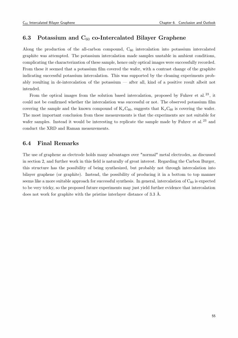
C60 Intercalated Bilayer Graphene Chapter 6. Conclusion and Outlook
6.3 Potassium and C60 co-Intercalated Bilayer Graphene
Along the production of the all-carbon compound, C60 intercalation into potassium intercalated
graphite was attempted. The potassium intercalation made samples unstable in ambient conditions,
complicating the characterization of these sample, hence only optical images were successfully recorded.
From these it seemed that a potassium film covered the wafer, with a contrast change of the graphite
indicating successful potassium intercalation. This was supported by the cleaning experiments prob-
ably resulting in de-intercalation of the potassium — after all, kind of a positive result albeit not
intended.
From the optical images from the solution based intercalation, proposed by Fuhrer et al. 23 , it
could not be confirmed whether the intercalation was successful or not. The observed potassium film
covering the sample and the known compound of KxC60, suggests that KxC60 is covering the wafer.
The most important conclusion from these measurements is that the experiments are not suitable for
wafer samples. Instead it would be interesting to replicate the sample made by Fuhrer et al. 23 and
conduct the XRD and Raman measurements.
6.4 Final Remarks
The use of graphene as electrode holds many advantages over "normal" metal electrodes, as discussed
in section 2, and further work in this field is naturally of great interest. Regarding the Carbon Burger,
this structure has the possibility of being synthesized, but probably not through intercalation into
bilayer graphene (or graphite). Instead, the possibility of producing it in a bottom to top manner
seems like a more suitable approach for successful synthesis. In general, intercalation of C60 is expected
to be very tricky, so the proposed future experiments may just yield further evidence that intercalation
does not work for graphite with the pristine interlayer distance of 3.3 Å.
55


Appendix A
Device Fabrication
Below are the optimized experimental details and recipes used throughout the project
UV-lithography
1. Disperse wafer in Acetone and sonicate for 10 min
2. Disperse in IPA and sonicate for 5 min
3. Blow dry with N2
4. Bake at 185C for 5 min. Allow to cool afterwards
5. Spin resist (AZ1505) at 4000 rpm in 45 s
6. Clean masks with Acetone and IPA and blow dry with N2
7. To remove edge beads expose with appropriate mask for 30 s
8. Change mask to desired design and expose for 4 s
9. Develop in AZ400K (1:4 in millipore water) for 30 s
10. Rinse in millipore water
11. Blow dry with N2
12. Plasma etch for 20 s
E-beam Lithography
1. Disperse wafer in Acetone and sonicate for 10 min
2. Disperse in IPA and sonicate for 5 min
3. Blow dry with N2
4. Bake at 185C for 3 min. Allow to cool afterwards
5. Spin 4% PMMA at 4000 rpm in 45 s
6. Bake at 185C for 3 min. Allow to cool afterwards
7. Do desired E-beam lithography
57

Appendix A. Device Fabrication C60 Intercalated Bilayer Graphene
8. Develop in MBIK:IPA (1:3) for 60 s
9. Disperse in IPA for 30 s
10. Blow dry with N2
Etching
1. Prepare two beakers, one with millipore water and one (NOT GLASS) with an Ammoniumfluoride - hydrofluoric acid mixture from SigmaAldrich78
2. Put wafer in the etching solution for appropriate amount of time (etching rate 1.3 nm)
3. Directly transfer the wafer to millipore water
4. Blow dry with N2
Metal Evaporation
1. Evaporate wanted metal(s)
2. Develop in PG remover for 1h
3. If development not complete try sonication in PG remover or heating to 80C
Expanded Graphite
1. Natural graphite are dispersed in fuming sulfuric acid (oleum) for 12h-16h
2. Rinse in millipore water
Quartz Ampoule Cleaning
1. Disperse in Acetone and sonicate for 10 min
2. Disperse in IPA and sonicate for 5 min
3. Blow dry with N2
4. Plasma etch for 5 min
Thermal C60 Intercalation
1. Prepare a clean quartz ampoule with a graphite sample and C60.
2. Evacuate for at least 1h to reach a pressure < 5 · 10−6 mbar
3. Seal quartz ampoule and heat to 600C for 2 weeks
58

C60 Intercalated Bilayer Graphene Appendix A. Device Fabrication
Potassium Intercalation
1. Prepare a large heptane bath
2. Take a piece Potassium, wipe off most of the mineral oil, and transfer directly to the heptane.
3. Use a scalpel to cut away some of the oxide layer, to reveal the shine metal. Do this in theheptane bath
4. A piece of clean Potassium is prepared, and another beaker is prepared with heptane and puton a weight capable of measuring with a precision of 0.1 mg
5. Weigh the small piece (target weight is 1-3 mg). Remember to wipe of most of the heptane,before weighing
6. Prepare a cleaned quartz ampoule with your graphene/graphite sample
7. Quickly transfer the potassium piece to the quartz ampoule and evacuate for at least 1h. Pressure< 5 · 10−6 mbar
8. Seal quartz tube and heat to 300C for 3h
Solvent C60 Intercalation
1. Prepare a Pyrex glass with a C60-saturated dry benzene solution
2. The quartz tube containing the potassium intercalated sample is smashed with a hammer, andthe sample is directly transferred to the solution. It can be ease the process to do an intermediatestep, where the sample is transferred to a large beaker containing e.g. heptane.
3. The Pyrex glass is sealed and heated to 80C for at least one day
4.
Thermal co-Intercalation of Potassium and C60
1. Prepare a clean quartz ampoule with a graphite sample, potassium and C60.
2. Evacuate for at least 1h to reach a pressure < 5 · 10−6 mbar
3. Seal quartz ampoule
4. Heat the quartz tube to 300C for 3 hours
5. Heat the quartz tube to 600C for 2 weeks
59

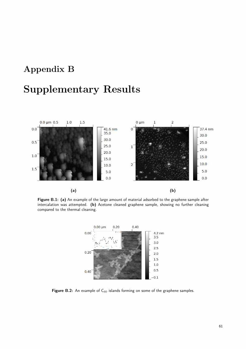
Appendix B
Supplementary Results
(a) (b)
Figure B.1: (a) An example of the large amount of material adsorbed to the graphene sample afterintercalation was attempted. (b) Acetone cleaned graphene sample, showing no further cleaningcompared to the thermal cleaning.
Figure B.2: An example of C60 islands forming on some of the graphene samples.
61

Appendix B. Supplementary Results C60 Intercalated Bilayer Graphene
(a) (b)
(c) (d)
Figure B.3: (a) AFM image of a MLG pre-intercalation attempt, with (c) being the height profileshowing a thickness of 7.05± 0.61 nm. (b) AFM image of a MLG post-intercalation attempt, with(d) being the height profile showing a thickness of 6.29± 0.47 nm.
Place 1 - Electrode - Pre-sheet Place 2 - Sheet Place 3 - Sheet Place 4 - Electrode - Post-sheet Linear Fit to Place 1 Linear Fit to Place 2 Linear Fit to Place 3 Linear Fit to Place 4
-0.004 -0.002 0.000 0.002 0.004
-3.00E-009
-2.00E-009
-1.00E-009
0.00E+000
1.00E-009
Cur
rent
[A]
Voltage [V]
(a) (b)
Figure B.4: (a) I-V curves corresponding to the points indicated in (b). (b) Optical image of thepristine FLG sample used for CAFM, with each site engaged denoted with a number and a +-sign.
62

C60 Intercalated Bilayer Graphene Appendix B. Supplementary Results
-0.006 -0.004 -0.002 0.000 0.002 0.004 0.006
-2.00E-009
-1.50E-009
-1.00E-009
-5.00E-010
0.00E+000
5.00E-010
1.00E-009
1.50E-009
2.00E-009
Cur
rent
[A]
Voltage [V]
Place1 - Electrode Place2 - Sheet Place3 - Sheet Place4 - Electrode Linear Fit of Sheet1 B Linear Fit of Sheet1 C Linear Fit of Sheet1 D Linear Fit of Sheet1 E
(a) (b)
Figure B.5: (a) I-V curves corresponding to the points indicated in (b). (b) Optical image of theattempted intercalated FLG sample used for CAFM, with each site engaged denoted with a numberand a +-sign.
-0.004 -0.002 0.000 0.002 0.004
-2.00E-009
-1.50E-009
-1.00E-009
-5.00E-010
0.00E+000
5.00E-010
1.00E-009
1.50E-009
2.00E-009
Cur
rent
[A]
Voltage [V]
Place1 - Electrode Place2 - Sheet Place3 - Sheet Place4 - Electrode Linear Fit to Place 1 Linear Fit to Place 2 Linear Fit to Place 3 Linear Fit to Place 4
Avg. Conduct Avg. ResistaPlace 1 3.67645E-7 2.72002E6Place 2 3.6133E-7 2.76756E6Place 3 3.59947E-7 2.77819E6Place 4 3.65402E-7 2.73671E6
(a) (b)
Figure B.6: (a) I-V curves corresponding to the points indicated in (b). (b) Optical image of theexpanded FLG sample used for CAFM, with each site engaged denoted with a number and a +-sign.
63


Appendix C
Supplementary Theory
Besides explaining some theoretical models in more details, this appendix includes extra calculationsthat to some extent are important for a better overview of the theory in this thesis or just somecalculations that were simple, but very tedious, time consuming and would aid the inexperiencedreader.
Tight Binding Model
For a detailed description of the band structure of graphene (SLG to FLG), the tight-binding modelyields a satisfactory result for the energy levels in proximity of the Fermi energy. Weakly interactingatoms are a crucial assumption in this model, which gives almost intact atomic orbitals after formingthe crystal.
A trial wave function are constructed as the sum between the wave functions for each of the twosub-lattices weighted with the complex functions a(k) and b(k)
ψ(k, r) = a(k)ψA(k, r) + b(k)ψB(k, r)
The electronic wave function for the two sub-lattices can be constructed from a linear combination ofatomic pz-orbitals, φs(r −Rs),
ψs(k, r) =1√N
∑
Rs
eikRsφs(r−Rs)
with s = [A,B]. Searching for solution to the Schrödinger equation, Hψ(k, r) = E(k)ψ(k, r), bymultiplying with ψ∗(k, r), yields (vector representation)
(a∗(k), b∗(k))H
(
a(k)b(k)
)
= E(k)(a∗(k), b∗(k))S
(
a(k)b(k)
)
where the 2x2 matrices (both H and S) are given as
H =
(
HAA HAB
HBA HBB
)
=
(
HAA HAB
H∗AB HAA
)
S =
(
SAA SAB
SBA SBB
)
=
(
SAA SAB
S∗AB SAA
)
where Hss′ = 〈Ψs|H|Ψs′〉 and Sss′ = 〈Ψs|Ψs′〉. As SLG contains two different carbon atoms in the unitcell, which by all practical means are indistinguishable, HAA = HBB and HBA = H∗
AB. For the overlap
65

Appendix C. Supplementary Theory C60 Intercalated Bilayer Graphene
matrix, S, it is assumed that the atomic wave functions are normalized, yielding SAA = SBB = 1 (theoverlap between two normalized identical wave functions is 1).
Including both the tight-binding Hamiltonian and the overlap matrix, for a 2D material with twodifferent atoms in the unit cell, one ends up with the following secular equation to solve
det [H− ES] = 0 (C.1)
Solving the determinant in equation C.1, yields
E =2HAASAA −H∗
ABSAB −HABS∗
AB±
√
(2HAASAA −H∗AB
SAB −HABS∗AB
)2 − 4(H2
AA−H∗
ABHAB)(S2
AA− S∗
ABSAB)
2(S2
AA− S∗
ABSAB)
With inspiration from Reich et al. 70 , this equation can be written on the form
E =2E0 − E1 ±
√
(2E0 − E1 − 4E2E3)
2E3
by substitution of the following definitions
E0 ≡ HAASAA E1 ≡ H∗ABSAB +HABS
∗AB
E2 ≡ H2AA −H∗
ABHAB E3 ≡ S2AA − S∗
ABSAB
The matrix elements are
HAA =
1√N
∑
RA
e−ikRA 〈φ2pz (r−RA)|
H
1√N
∑
RA′
eikRA′ |φ2pz (r−RA′)〉
=1
N
∑
RA
∑
RA′
eik(RA′−RA) 〈φpz(r−RA)|H|φpz(r−RA′)〉
Nearest-Neighbour Approximation For simplicity, only interactions between adjacent carbonatoms are accounted for, i.e. nearest-neighbour approximation, which for HAA only gives a result forA = A′
HAA ≈ 1
N
∑
RA
〈φ2pz(r−RA)|H|φ2pz (r−RA)〉 = ǫ2pz
ǫ2pz is the atomic energy for atom in the 2D crystal (the Hamiltonian contains the crystal potential).
66

C60 Intercalated Bilayer Graphene Appendix C. Supplementary Theory
In a similar way can HAB and SAB be determined.
HAB =
1√N
∑
RA
e−ikRA 〈φ2pz (r−RA)|
H
1√N
∑
RB
eikRB |φ2pz(r−RB)〉
=1
N
∑
RA
∑
RB
eik(RB−RA) 〈φpz(r−RA)|H|φpz(r−RB)〉
=1
N
∑
RA
∑
Ri
eik(RA−RA+Ri) 〈φpz(r−RA)|H|φpz(r−RA −Ri)〉
≈ γ0f(k) , with γ0 = 〈φpz(r−RA)|H|φpz (r−RA −Ri)〉
SAB =1
N
∑
RA
∑
Ri
eik(RA−RA+Ri) 〈φpz(r−RA)|φpz (r−RA −Ri)〉
≈ s0f(k) , with s0 = 〈φpz(r−RA)|φpz (r−RA −Ri)〉
Here γ0 and s0 are the transfer integral and overlap integral between nearest neighbours, respectively,and f(k) = eikR1 + eikR2 + eikR3 , with R1 = a(−1/2, 1/(2
√3)), R2 = and R3 =, the three vectors to
the nearest neighbours.Inserting the calculated matrix elements in the energy dispersion equation, yields:
E(k) =2ǫ2pz − 2γ0s0f(k)
2 ±√
(2γ0s0f(k)2 − 2ǫ2pz)2 − 4(1− s20f(k)
2)(ǫ22pz − γ20f(k)2)
1− s20f(k)2
=ǫ2pz ± γ0
√
|f(k)|21± s0
√
|f(k)|2
The three parameters ǫ2pz , s0 and γ0, can be estimated by fitting either experimental or first-principlescalculation data70. The sum of phase factors, f(k), is
f(k) = 2 cos(a
2kx
)
exp
(
ia
2√3ky
)
+ exp
(
−i a√3ky
)
67


Bibliography
[1] DSL Abergel, V Apalkov, J Berashevich, K Ziegler, and T Chakraborty. Properties of graphene:a theoretical perspective. Advances in Physics, 59(4):261–482, 2010.
[2] W Andreoni, P Giannozzi, and M Parrinello. Molecular-structure and chemical bonding in k3c60and k6c60. Physical Review B, 51(4):2087–2097, Jan 15 1995.
[3] S Aronson, C Frishberg, and G Frankl. Thermodynamic properties of the graphite-bisulfatelamellar compounds. Carbon, 9(6):715–72, 1971.
[4] A Aviram and MA Ratner. Molecular rectifiers. Chemical Physics Letters, 29(2):277–283, 1974.
[5] DM Basko, S Piscanec, and AC Ferrari. Electron-electron interactions and doping dependence ofthe two-phonon raman intensity in graphene. Physical Review B, 80(16), Oct 2009.
[6] C Berger, ZM Song, TB Li, XB Li, AY Ogbazghi, R Feng, ZT Dai, AN Marchenkov, EH Conrad,PN First, and WA de Heer. Ultrathin epitaxial graphite: 2d electron gas properties and a routetoward graphene-based nanoelectronics. Journal of Physical Chemistry B, 108(52):19912–19916,Dec 30 2004.
[7] G Binnig, CF Quate, and C Gerber. Atomic force microscope. Physical Review Letters, 56(9):930–933, Mar 3 1986.
[8] P Blake, EW Hill, AH Castro Neto, KS Novoselov, D Jiang, R Yang, TJ Booth, and AK Geim.Making graphene visible. Apllied Physics Letters, 91(6), Aug 6 2007.
[9] F Boerrnert, L Fu, S Gorantla, M Knupfer, B Buechner, and MH Ruemmeli. Programmablesub-nanometer sculpting of graphene with electron beams. ACS Nano, 6(11):10327–10334, Nov2012.
[10] Bruker, Jun 2013. URL http://www.bruker.com.
[11] EV Castro, KS Novoselov, SV Morozov, NMR Peres, JMBL Dos Santos, J Nilsson, F Guinea,AK Geim, and AH Castro Neto. Biased bilayer graphene: Semiconductor with a gap tunable bythe electric field effect. Physical Review Letters, 99(21), Nov 23 2007.
[12] AH Castro Neto, F Guinea, NMR Peres, KS Novoselov, and AK Geim. The electronic propertiesof graphene. Reviews of Modern Physics, 81(1):109–162, Jan-Mar 2009.
[13] GH Chen, DJ Wu, WU Weng, and CL Wu. Exfoliation of graphite flake and its nanocomposites.Carbon, 41(3):619–621, 2003.
[14] J Chen, MA Reed, AM Rawlett, and JM Tour. Large on-off ratios and negative differentialresistance in a molecular electronic device. Science, 286(5444):1550–1552, Nov 19 1999.
69

Bibliography C60 Intercalated Bilayer Graphene
[15] Z Chen, YM Lin, MJ Rooks, and P Avouris. Graphene nano-ribbon electronics. Physica E-Low-
Dimensional Systems & Nanostructures, 40(2):228–232, Dec 2007.
[16] J Cho, J Smerdon, L Gao, O Suezer, JR. Guest, and NP. Guisinger. Structural and electronicdecoupling of c-60 from epitaxial graphene on sic. Nano Letters, 12(6):3018–3024, Jun 2012.
[17] MS Dresselhaus and G Dresselhaus. Intrecalation Compounds of Graphite. Advances in Physics,30(2):139–326, 1981.
[18] MS Dresselhuas, G Dresselhaus, and PC Eklund. Science of Fullerenes and Carbon Nanotubes.Academic Press, 1996.
[19] G Eda, G Fanchini, and M Chhowalla. Large-area ultrathin films of reduced graphene oxide as atransparent and flexible electronic material. Nature Nanotechnology, 3(5):270–274, May 2008.
[20] H Fernandezmoran. Single-crystal of graphite and of mica as specimen support for electronmicroscopy. Journal of Applied Physics, 31(10):1840, 1960.
[21] AC Ferrari and DM Basko. Raman spectroscopy as a versatile tool for studying the properties ofgraphene. Nature Nanotechnology, 8(4):235–246, Apr 2013.
[22] AC Ferrari, JC Meyer, V Scardaci, C Casiraghi, M Lazzeri, F Mauri, S Piscanec, D Jiang,KS Novoselov, S Roth, and AK Geim. Raman spectrum of graphene and graphene layers. Physical
Review Letters, 97(18), Nov 3 2006.
[23] MS Fuhrer, JG Hou, XD Xiang, and A Zetil. C60 intercalated graphite - predictions and experi-ments. Solid State Communications, 90(6):357–360, May 1994.
[24] AK Geim and KS Novoselov. The rise of graphene. Nature Materials, 6(3):183–191, Mar 2007.
[25] MO Goerbig. Electronic properties of graphene in a strong magnetic field. Review of Modern
Physics, 83:1193–1243, Nov 2011.
[26] A Grüneis, C Attaccalite, L Wirtz, H Shiozawa, R Saito, T Pichler, and A Rubio. Tight-bindingdescription of the quasiparticle dispersion of graphite and few-layer graphene. Physical Review
B, 78:205425, Nov 2008.
[27] Arnold Gruppe, Feb 2013. URL http://www.arnold-gruppe.de.
[28] V Gupta, P Scharff, K Risch, H Romanus, and R Muller. Synthesis of c-60 intercalated graphite.Solid State Communications, 131(3-4):153–155, Jul 2004.
[29] V Gupta, P Scharff, LC Abelmann, and L Spiess. C-60 intercalated graphite: A new form ofcarbon. Fullerenes Nanotubes and Carbon Nanostructures, 13(1):427–430, May 24-28 2005.
[30] CR Hansen, TJ Sørensen, M Glyvradal, J Larsen, SH Eisenhardt, T Bjørnholm, MM Nielsen,R Feidenhans’l, and BW Laursen. Structure of the buried metal-molecule interface in organicthin film devices. Nano Letters, 9(3):1052–1057, 2009.
[31] AF Hebard, MJ Rosseinsky, RC Haddon, DW Murphy, SH Glarum, TTM Palstra, AP Ramirez,and AR Kortan. Superconductivity at 18-k in potassium-doped c-60. Nature, 350(6319):600–601,Apr 18 1991.
[32] WC Hu, K Sarveswaran, M Lieberman, and GH Bernstein. Sub-10 nm electron beam lithographyusing cold development of poly(methylmethacrylate). Journal of Vacuum Science & Technology
B, 22(4):1711–1716, Jul-Aug 2004.
70
C60 Intercalated Bilayer Graphene Bibliography
[33] IMSI/Design. Designcad 3d max, Jul 2013. URL http://www.imsidesign.com/.
[34] National Instruments. Labview, Aug 2013. URL http://sine.ni.com/np/app/main/p/docid/
nav-104/lang/da/.
[35] HG Jee, JH Han, HN Hwang, YD Kim, and CC Hwang. Adsorption and desorption of fullereneon graphene/sic(0001). Surface Science, 605(7-8):649–653, Apr 2011.
[36] JE Jones. On the determination of molecular fields. ii. from the equation of state of a gas.Proceedings of the Royal Society of London. Series A, 106(738):463–477, 1924.
[37] KS Kim, Y Zhao, H Jang, SY Lee, JM Kim, KS Kim, JH Ahn, P Kim, JY Choi, and BH Hong.Large-scale pattern growth of graphene films for stretchable transparent electrodes. Nature, 457(7230):706–710, Feb 5 2009.
[38] DV Kosynkin, AL Higginbotham, A Sinitskii, JR Lomeda, A Dimiev, BK Price, and JM Tour.Longitudinal unzipping of carbon nanotubes to form graphene nanoribbons. Nature, 458(7240):872–U5, Apr 16 2009.
[39] W Kratschmer, LD Lamb, K Fostiropoulos, and DR Huffman. Solid c-60 - a new form of carbon.Nature, 347(6291):354–358, Sep 27 1990.
[40] HW Kroto, JR Heath, SC Obrien, RF Curl, and RE Smalley. C-60 - buckminsterfullerene. Nature,318(6042):162–163, 1985.
[41] HW Kroto, AW Allaf, and SP Balm. C-60 - buckminsterfullerene. Chemical Reviews, 91(6):1213–1235, Sep-Oct 1991.
[42] C Lee, X Wei, JW Kysar, and J Hone. Measurement of the elastic properties and intrinsicstrength of monolayer graphene. Science, 321(5887):385–388, Jul 18 2008.
[43] NJ Lee, JW Yoo, YJ Choi, CJ Kang, DY Jeon, DC Kim, S Seo, and HJ Chung. The interlayerscreening effect of graphene sheets investigated by kelvin probe -force microscopy. APPLIED
PHYSICS LETTERS, 95(22), Nov 30 2009.
[44] G Li, HT Zhou, LD Pan, Y Zhang, JH Mao, Q Zou, HM Guo, YL Wang, SX Du, and HJ Gao. Self-assembly of c-60 monolayer on epitaxially grown, nanostructured graphene on ru(0001) surface.Applied Physics Letters, 100(1):013304, 2012.
[45] LM Malard, MA Pimenta, G Dresselhaus, and MS Dresselhaus. Raman spectroscopy in graphene.Physics Report-Review Section of Physics Letters, 473(5-6):51–87, Apr 2009.
[46] CA Martin, D Ding, JK Sorensen, T Bjornholm, JM van Ruitenbeek, and HSJ van der Zant.Fullerene-based anchoring groups for molecular electronics. Journal of the American Chemical
Society, 130(40):13198–13199, Oct 8 2008.
[47] Delta Mask, May 2013. URL http://www.deltamask.nl/.
[48] MathWorks. Matlab, Jul 2013. URL http://www.mathworks.se/products/matlab/.
[49] E McCann. Asymmetry gap in the electronic band structure of bilayer graphene. Physical Review
B, 74(16), Oct 2006.
[50] E McCann and VI Fal’ko. Landau-level degeneracy and quantum hall effect in a graphite bilayer.Physical Review Letters, 96(8), Mar 3 2006.
71

Bibliography C60 Intercalated Bilayer Graphene
[51] E McCann and M Koshino. The electronic properties of bilayer graphene. Reports on Progress
in Physics, 76(5), May 2013.
[52] AM Moore, AA Dameron, BA Mantooth, RK Smith, DJ Fuchs, JW Ciszek, F Maya, YX Yao,JM Tour, and PS Weiss. Molecular engineering and measurements to test hypothesized mecha-nisms in single molecule conductance switching. Journal of the American Chemical Society, 128(6):1959–1967, Feb 15 2006.
[53] SV Morozov, KS Novoselov, MI Katsnelson, F Schedin, DC Elias, JA Jaszczak, and AK Geim.Giant intrinsic carrier mobilities in graphene and its bilayer. Physical Review Letters, 100(1),Jan11 2008.
[54] K Moth-Poulsen and T Bjornholm. Molecular electronics with single molecules in solid-statedevices. Nature Nanotechnology, 4(9):551–556, Sep 2009.
[55] µMasch. Spm tip producer, Jul 2013. URL http://www.spmtips.com/.
[56] D Necas and P Klapetek. Gwyddion: an open-source software for SPM sata analysis, 2012. URLhttp://gwyddion.net/.
[57] J Nilsson, AH Castro Neto, F Guinea, and NMR Peres. Electronic properties of bilayer andmultilayer graphene. Physical Review B, 78(4), Jul 2008.
[58] DE Nixon and GS Parry. Formation and structure of potassium graphites. Journal of Physics
D-Applied Physics, 1(3):291–&, 1968.
[59] KS Novoselov, AK Geim, SV Morozov, D Jiang, Y Zhang, SV Dubonos, IV Grigorieva, andAA Firsov. Electric field effect in atomically thin carbon films. Science, 306(5696):666–669, Oct22 2004.
[60] KS Novoselov, AK Geim, SV Morozov, D Jiang, MI Katsnelson, IV Grigorieva, SV Dubo-nos,and AA Firsov. Two-dimensional gas of massless dirac fermions in graphene. Nature, 438(7065):197–200, Nov 10 2005.
[61] KS Novoselov, Z Jiang, Y Zhang, SV Morozov, HL Stormer, U Zeitler, JC Maan, GS Boebinger,P Kim, and AK Geim. Room-temperature quantum hall rffect in graphene. Science, 315(5817):1379, Mar 9 2007.
[62] P O’Brien, H Craighead, H Kroto, and MS Amer. Raman Spectroscopy Fullerenes and Nanotech-
nology. RSC Nanoscience and Nanotechnology. The Royal Society of Chemistry, 2010.
[63] T Ohta, A Bostwick, T Seyller, K Horn, and E Rotenberg. Controlling the Electronic Structureof Bilayer Graphene. Science, 313(5789):951–954, Aug 18 2006.
[64] OriginLab. Originpro 8.6, Aug 2013. URL http://www.originlab.com/.
[65] TTM Palstra, O Zhou, Y Iwasa, PE Sulewski, RM Fleming, and BR Zegarski. Superconductivityat 40k in cesium doped c-60. Solid State Communications, 93(4):327–330, Jan 1995.
[66] H Park, AKL Lim, AP Alivisatos, J Park, and PL McEuen. Fabrication of Metallic Electrodeswith Nanometer Separation by Electromigration. Applied Physics Letters, 75(2):301–303, Jul 121999.
[67] NMR. Peres. The electronic properties of graphene and its bilayer. Vacuum, 83(10):1248–1252,Jun 16 2009.
72

C60 Intercalated Bilayer Graphene Bibliography
[68] NMR Peres. Colloquium: The transport properties of graphene: An introduction. Reviews of
Modern Physics, 82(3):2673–2700, Sep 15 2010.
[69] MA Reed, C Zhou, CJ Muller, TP Burgin, and JM Tour. Conductance of a Molecular Junction.Science, 278(5336):252–254, Oct 10 1997.
[70] S Reich, J Maultzsch, C Thomsen, and P Ordejón. Tight-binding description of graphene. Physical
Review B, 66:035412, Jul 2002.
[71] C Rogero, JI Pascual, J Gomez-Herrero, and AM Baro. Resolution of site-specific bondingproperties of c-60 adsorbed on au(111). Journal of Chemical Physics, 116(2):832–836, Jan 82002.
[72] R Saito, G Dresselhaus, and MS Dresselhaus. Physical Properties of Carbon Nanotube. ImperialCollege Press, 1998.
[73] S Saito and A Oshiyama. Ionic metal kxc60 - cohesion and energy-bands. Physical Review B, 44(20):11536–11539, Nov 15 1991.
[74] S Saito and A Oshiyama. Cohesive mechanism and energy-bands of solid c60. Physical Review
Letters, 66(20):2637–2640, May 20 1991.
[75] S Saito and A Oshiyama. Design of c(60)-graphite cointercalation compounds. Physical Review
B, 49(24):17413–17419, Jun 15 1994.
[76] F Schwierz. Graphene transistors. Nature Nanotechnology, 5(7):487–496, Jul 2010.
[77] SHR Sena, JM Pereira, Jr., GA Farias, FM Peeters, and RN Costa Filho. The electronic propertiesof graphene and graphene ribbons under simple shear strain. Journal of Physics-Condensed
Matter, 24(37), Sep 19 2012.
[78] Sigma-Aldrich, Dec 2012. URL http://www.sigmaaldrich.com.
[79] JK Sorensen, J Fock, AH Pedersen, AB Petersen, K Jennum, K Bechgaard, K Kilsa, V Geskin,J Cornil, T Bjornholm, and MB Nielsen. Fulleropyrrolidine end-capped molecular wires formolecular electronics-synthesis, spectroscopic, electrochemical, and theoretical characterization.Journal of Organic Chemistry, 76(1):245–263, Jan 7 2011.
[80] K Tanigaki, TW Ebbesen, S Saito, J Mizuki, JS Tsai, Y Kubo, and S Kuroshima. Superconduc-tivity at 33-k in csxrbyc60. Nature, 352(6332):222–223, Jul 18 1991.
[81] P Venezuela, M Lazzeri, and F Mauri. Theory of double-resonant raman spectra in graphene:Intensity and line shape of defect-induced and two-phonon bands. Physical Review B, 84:035433,Jul 2011.
[82] M. Švec, P. Merino, Y. J. Dappe, C. González, E. Abad, P. Jelínek, and J. A. Martín-Gago. vander waals interactions mediating the cohesion of fullerenes on graphene. Physical Review B, 86:121407, Sep 2012.
[83] PR Wallace. The band theory of graphite. Physical Review, 71(9):622–634, 1947.
[84] R Wang, S Wang, X Wang, JAS Meyer, P Hedegard, BW Laursen, Z Cheng, and X Qiu. Chargetransfer and current fluctuations in single layer graphene transistors modified by self-assembledc60 adlayers. Small, 9:2420–6, Jul 22 2013.
73

Bibliography C60 Intercalated Bilayer Graphene
[85] X Wang and H Dai. Etching and narrowing of graphene from the edges. Nature Chemistry, 2(8):661–665, Aug 2010.
[86] Wieweb. Clewin 4, Dec 2012. URL http://www.wieweb.com/ns6/index.html.
[87] G Xie, Z Shi, R Yang, D Liu, W Yang, M Cheng, D Wang, D Shi, and G Zhang. Graphene edgelithography. Nano Letters, 12(9):4642–4646, Sep 2012.
[88] O Zhou, JE Fischer, N Coustel, S Kycia, Q Zhu, AR McGhie, WJ Romanow, JP McCauley,AB Smith, and DE Cox. Structure and bonding in alkali-metal-doped c60. Letters to Nature,351:462–464, Jun 1991.
74