Embed Size (px)
Citation preview

Copyright 2008, Toshiba Corporation.
CAE Flow in the Development for the Digital Equipments
Motochika OkanoPC Development Center
Toshiba Corporation2008/09/19(Fri)

Copyright 2008, Toshiba Corporation.
CAE Flow for PCB Design
Chip / Package / PCB Modeling

Copyright 2008, Toshiba Corporation.
CAE Flow for PCB Design
Chip / Package / PCB Modeling

4
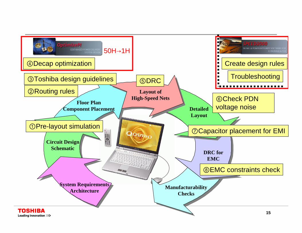
PCB Design Flow
DRC forEMC
DetailedLayout
Circuit DesignSchematic
System RequirementsArchitecture
Floor PlanComponent Placement
ManufacturabilityChecks
Layout ofHigh-Speed Nets

5
DRC forEMC
DetailedLayout
Circuit DesignSchematic
System RequirementsArchitecture
Floor PlanComponent Placement
ManufacturabilityChecks
Layout ofHigh-Speed Nets
Create design rules
Troubleshooting③Toshiba design guidelines
④Decap optimization
⑤DRC
⑥Check PDN voltage noise
⑦Capacitor placement for EMI
⑧EMC constraints check
①Pre-layout simulation
②Routing rules
PCB Design Flow

6
DRC forEMC
DetailedLayout
Circuit DesignSchematic
System RequirementsArchitecture
Floor PlanComponent Placement
ManufacturabilityChecks
Layout ofHigh-Speed Nets
Create design rules
Troubleshooting③Toshiba design guidelines
④Decap optimization
⑤DRC
⑥Check PDN voltage noise
⑦Capacitor placement for EMI
⑧EMC constraints check
①Pre-layout simulation
②Routing rules
PCB Design Flow

7
Decaps
↓
DC-DCConverter LSI
GND
VCC
Bulk Caps
L1L2L3
C1C2
Observationof PDN impedance
Case Study for Decap Optimization

8
CPU
Bulk caps Decoupling Capicators
< Typical Methodology (before OptimizePI) > 1. Identify decap placement locations from CPU supplier specifications

9
2. Pickup possible decap combinations based on Design of Experimentapproach ( 1 hour for this design )
Bulk caps Decaps
45identifiedpossibleschemes

10
3. Simulation of impedance for all 45 combinations one by one. ( 1 hour per combination. This takes about 45 hours in total. )
Freq [Hz]
Impe
danc
e [O
hms]
Target Impedance

11
4. The best scheme, based on performance and cost, is identifiedby engineers. ( This typically takes 4 hours. )
A typical project takes 50 hoursfor decap optimization.

12
< OptimizePIis now used instead >
1. Automatically identify the best scheme in 1 hour.
Extract23 optimized
schemes
Target Impedance
Impedance profilefor all 23 schemes

13
2. Result with OptimizePI enables engineer to quickly select the bestscheme from the 23 candidates
Cost / Performance Trade-off
Impedance Results
14
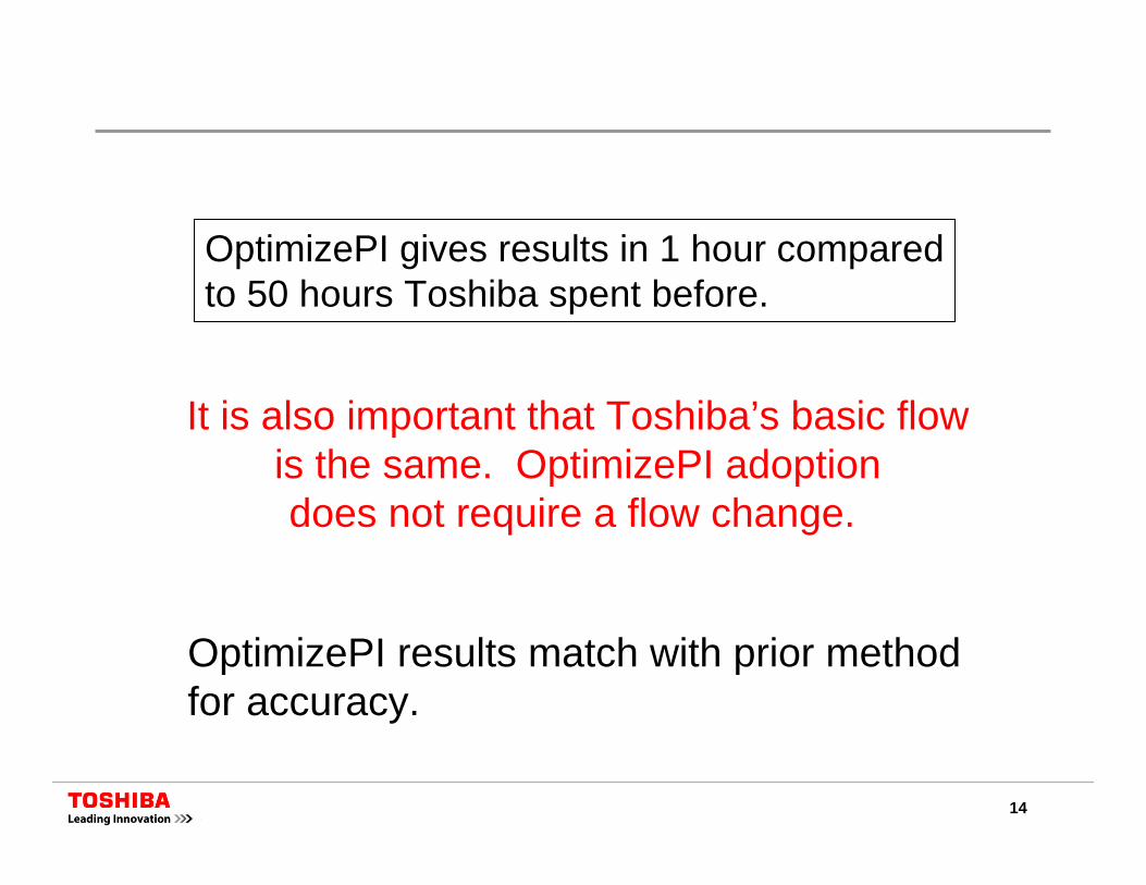
It is also important that Toshiba’s basic flowis the same. OptimizePI adoptiondoes not require a flow change.
OptimizePI gives results in 1 hour comparedto 50 hours Toshiba spent before.
OptimizePI results match with prior methodfor accuracy.
15
DRC forEMC
DetailedLayout
Circuit DesignSchematic
System RequirementsArchitecture
Floor PlanComponent Placement
ManufacturabilityChecks
Layout ofHigh-Speed Nets
Create design rules
Troubleshooting③Toshiba design guidelines
④Decap optimization
⑤DRC
⑥Check PDN voltage noise
⑦Capacitor placement for EMI
⑧EMC constraints check
①Pre-layout simulation
②Routing rules
50H→1H

Copyright 2008, Toshiba Corporation.
CAE Design Flow for PCB Design
Chip / Package / PCB Modeling

17
Methods to determine the target impedancefor PDN optimization
・LSI vendor provides – We use their information.
・LSI vendor doesn’t provide – We make our own calculations.

18
planning
Synthesis from RTL
Floor planning
Place & Route
RC Extraction
Pad IO (Bump) assignment
Chip Sign Off
Package selection
Fix package constraints
Package+PCB SI/PI/Thermal/EMI
Detailed route in PVP
Package + PCB SI/PI
Package Sign Off
Package+PCBpin map constraints
CPS Co-Optimization flow(in-hose tools)
Chip Design flow Package / PCB Design Flow
Opt
imiz
atio
n
Package +PCB EMI
CPS Co-Implementation & Sign Off
Impl
emen
tatio
n &
SO
2008/3Q 3rd Party tool
Timing closure
Package virtual prototype
SPICE mode complier
Final package design
Chip desing
PCB desing(Customer)
Detailed route in PVP
Chip PI
Pcake moeling
PKG/PCB PI
CPS-Co-verificationSignal & Power Integrity analysis
(customer + TOSHIBA)
Chip Power Integritytool
IO padplanner
CAE Effort by Semiconductor group at Toshiba
Nikkei Microdevices August, 2008

19
TIME
CPM Model
PCB
ICThe total chip power current is extracted
from all the power pin current observations.
CPM (Chip Power Model)includes parasitic of entire chip power delivery network
current currentballs
CU
RR
EN
T

20
Frequency
Fourier transform of CPM current waveforms
I = I(f)
Cur
rent
Den
sity

21
Frequency
Impe
danc
e)
The current spectrum in frequency domainis used to calculate target impedance.
Target Impedance

22
IC PackageModelModel

23
Frequency
Impe
danc
e
Impedance observedat IC power pins
Target Impedance

24
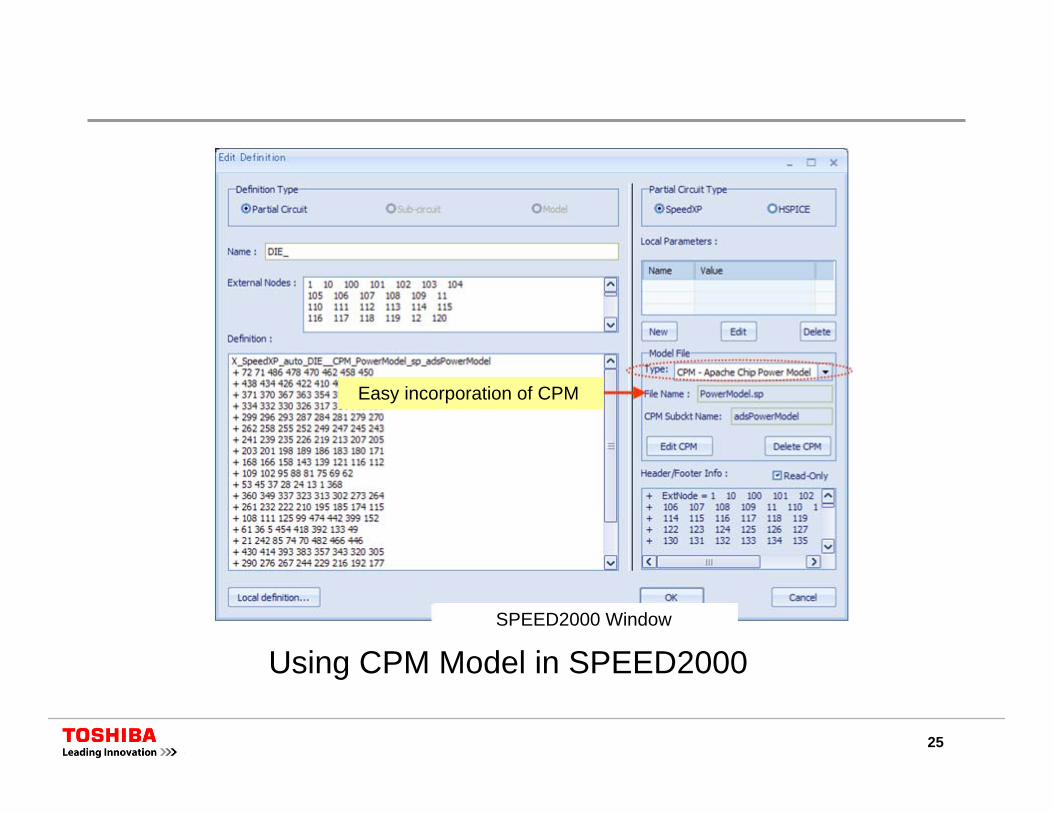
CPM and SPEED2000 used together
Importing CPM
Exporting Package model with CPP header
25
Using CPM Model in SPEED2000SPEED2000 Window
Easy incorporation of CPM

26
CPM model used as a noise source in SPEED2000 simulation.Far Field results show good correlation to measurements.
Frequency
Far F
ield
Mag
nitu
de fo
r PC
B EMI simulation by SPEED2000 with CPM
EMI measured results

27
Summary
CAE Utilization in PCB Design
- Decap optimization flow with OptimizePI
- CPM can help in calculating target impedance
- CPM can be used with SPEED2000 for EMC analysis

28