Embed Size (px)
Citation preview
CALICE ECAL/AHCAL Electronics 5-6 July 2010 @ DESY L.Caponetto, H.Mathez 1
Developments and Planning towards
1 m3 Technological
DHCAL Prototype
Didier BON, Luigi CAPONETTO, Christophe COMBARET Didier DELAUNAY, Rodolphe DELLA-NEGRA, Hervé MATHEZ,
Imad LAKTINEH, William TROMEUR
(CNRS IN2P3 IPNL)
Collaboration with LAL

CALICE ECAL/AHCAL Electronics 5-6 July 2010 @ DESY L.Caponetto, H.Mathez 2
Beam
DIF
DIF
DIF
gas
gas
H.V
Technological semi-digital hadronic calorimeter project
40 Sqm•Detector•PCB
CALICE ECAL/AHCAL Electronics 5-6 July 2010 @ DESY L.Caponetto, H.Mathez 3
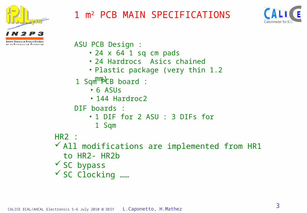
1 m2 PCB MAIN SPECIFICATIONS
ASU PCB Design :• 24 x 64 1 sq cm pads• 24 Hardrocs Asics chained• Plastic package (very thin 1.2 mm)
1 Sqm PCB board : • 6 ASUs• 144 Hardroc2
DIF boards : • 1 DIF for 2 ASU : 3 DIFs for 1 Sqm
HR2 : All modifications are implemented from HR1 to
HR2- HR2b SC bypass SC Clocking ……

CALICE ECAL/AHCAL Electronics 5-6 July 2010 @ DESY L.Caponetto, H.Mathez 4
ASU PCB DESIGN50 cm
36
cm
1536 pads on Bottom Layer
DIF connector
ASU to ASU connector
ASU to ASU connector
Power and Gnd ConnectorASU to ASU on X axis
GND Connection ASU to ASU on Y axis
Y
X
HR1
HR24
GND Connection ASU to ASU on Y axis
Buffers(Other signals)
Buffers(Clocks)
• Buried and Blind Vias are implemented
All buffers are optional(Normally not mounted)

CALICE ECAL/AHCAL Electronics 5-6 July 2010 @ DESY L.Caponetto, H.Mathez 5
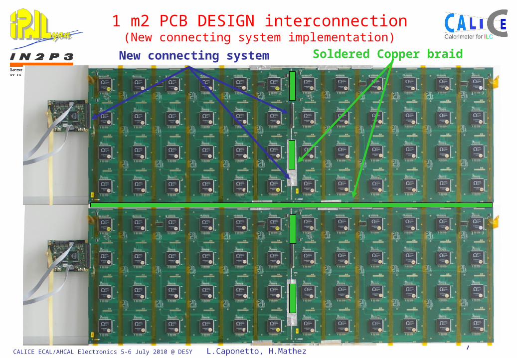
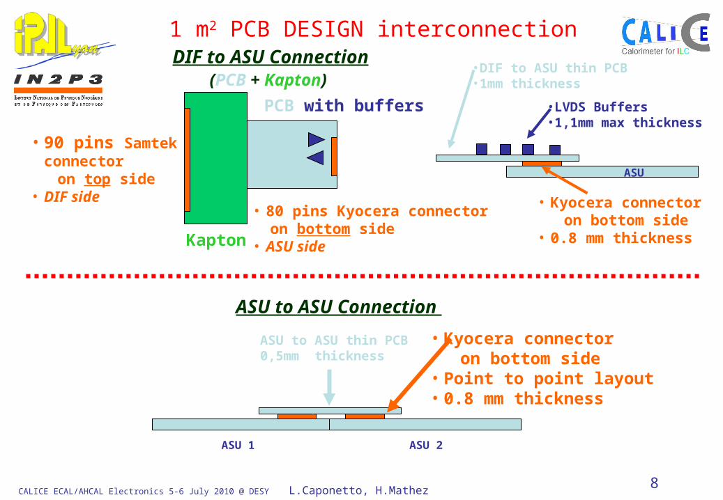
1 m2 PCB DESIGN interconnection
DIF Board
• Problems with 90 pins Samtek connector : Pad are teared off after several connect/disconnect DIF board
• Added a kapton/PCB cable between board and ASU to reduce connections problems• New connector on ASU board• Kyocera connector used for the ECAL

CALICE ECAL/AHCAL Electronics 5-6 July 2010 @ DESY L.Caponetto, H.Mathez 6
1 m2 PCB DESIGN interconnection
1 DIF for 2 ASUs
DIF Board
9216 pads on Bottom Layer
Same Kyocera connector • ASU to ASU• DIF to ASU
• Shielding between ASU at any place where it is possible• Soldered Copper braid
CALICE ECAL/AHCAL Electronics 5-6 July 2010 @ DESY L.Caponetto, H.Mathez 7
New connecting system Soldered Copper braid
1 m2 PCB DESIGN interconnection(New connecting system implementation)
CALICE ECAL/AHCAL Electronics 5-6 July 2010 @ DESY L.Caponetto, H.Mathez 8
ASU to ASU Connection
ASU 1 ASU 2
ASU to ASU thin PCB0,5mm thickness
• Kyocera connector on bottom side• Point to point layout• 0.8 mm thickness
1 m2 PCB DESIGN interconnectionDIF to ASU Connection
(PCB + Kapton)
• 80 pins Kyocera connector on bottom side• ASU side
• 90 pins Samtek connector
on top side• DIF side
PCB with buffers
Kapton
ASU
• Kyocera connector on bottom side• 0.8 mm thickness
•LVDS Buffers•1,1mm max thickness
•DIF to ASU thin PCB•1mm thickness
CALICE ECAL/AHCAL Electronics 5-6 July 2010 @ DESY L.Caponetto, H.Mathez 9
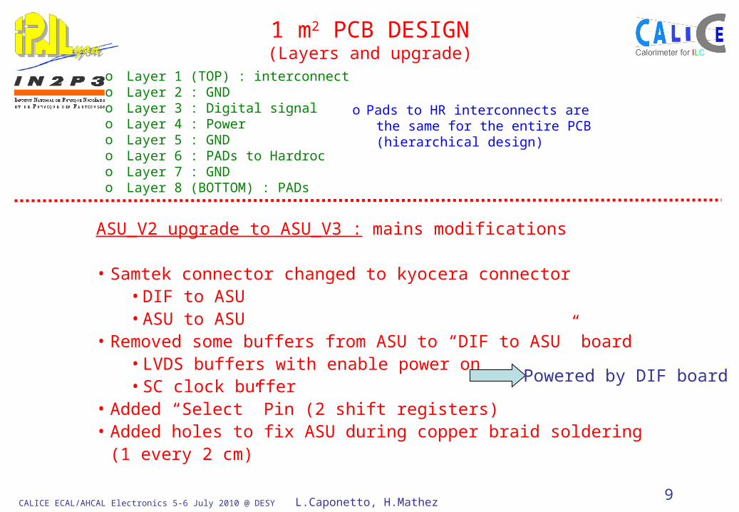
1 m2 PCB DESIGN(Layers and upgrade)
o Layer 1 (TOP) : interconnecto Layer 2 : GNDo Layer 3 : Digital signalo Layer 4 : Powero Layer 5 : GNDo Layer 6 : PADs to Hardroc o Layer 7 : GNDo Layer 8 (BOTTOM) : PADs
o Pads to HR interconnects are the same for the entire PCB (hierarchical design)
ASU_V2 upgrade to ASU_V3 : mains modifications
• Samtek connector changed to kyocera connector•DIF to ASU •ASU to ASU
• Removed some buffers from ASU to “DIF to ASU” board•LVDS buffers with enable power on •SC clock buffer
• Added “Select” Pin (2 shift registers)• Added holes to fix ASU during copper braid soldering
(1 every 2 cm)
Powered by DIF board
CALICE ECAL/AHCAL Electronics 5-6 July 2010 @ DESY L.Caponetto, H.Mathez 10
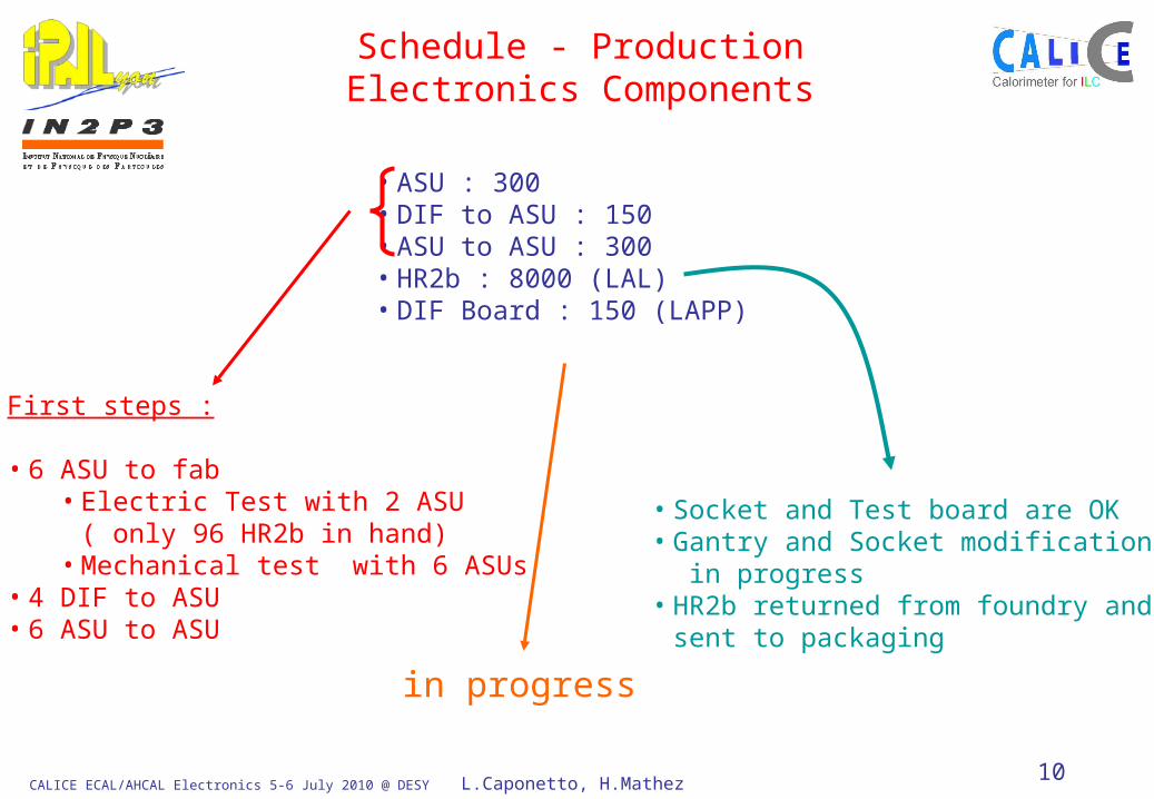
Schedule - ProductionElectronics Components
• ASU : 300 • DIF to ASU : 150• ASU to ASU : 300• HR2b : 8000 (LAL)• DIF Board : 150 (LAPP)
First steps :
• 6 ASU to fab• Electric Test with 2 ASU
( only 96 HR2b in hand)• Mechanical test with 6 ASUs
• 4 DIF to ASU• 6 ASU to ASU
• Socket and Test board are OK• Gantry and Socket modification
in progress• HR2b returned from foundry and
sent to packaging
in progress
CALICE ECAL/AHCAL Electronics 5-6 July 2010 @ DESY L.Caponetto, H.Mathez 11
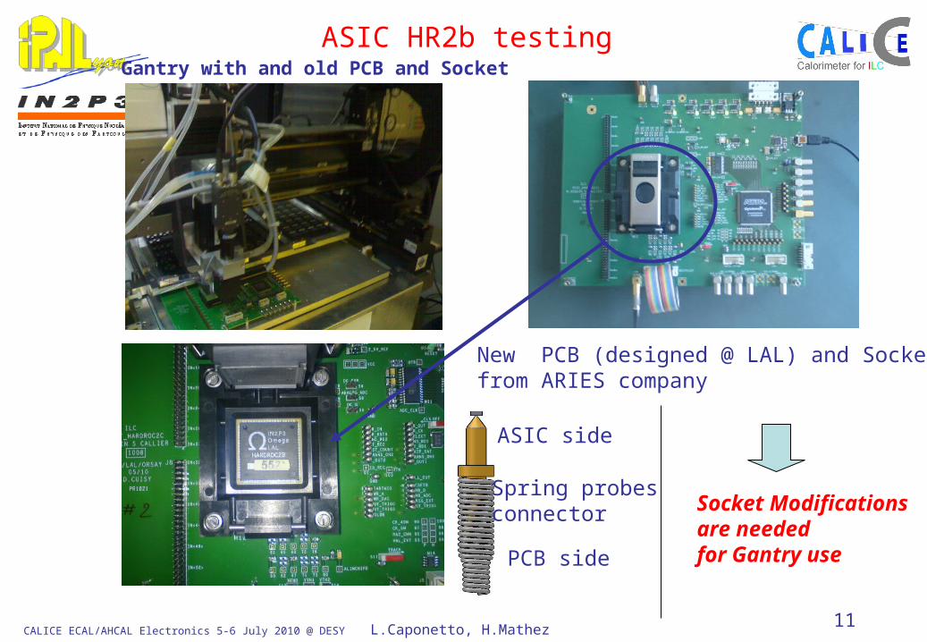
Gantry with and old PCB and Socket
New PCB (designed @ LAL) and Socketfrom ARIES company
Spring probes connector
ASIC side
PCB side
ASIC HR2b testing
Socket Modifications are neededfor Gantry use
CALICE ECAL/AHCAL Electronics 5-6 July 2010 @ DESY L.Caponetto, H.Mathez 12
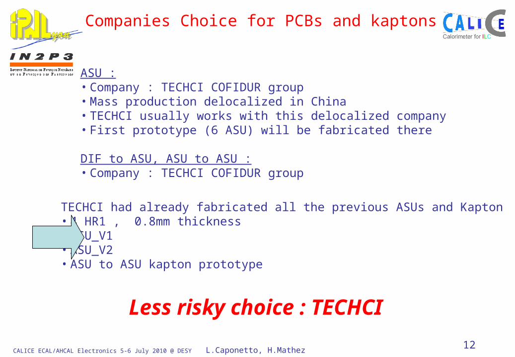
Companies Choice for PCBs and kaptons
ASU :• Company : TECHCI COFIDUR group• Mass production delocalized in China• TECHCI usually works with this delocalized company• First prototype (6 ASU) will be fabricated there
DIF to ASU, ASU to ASU :• Company : TECHCI COFIDUR group
TECHCI had already fabricated all the previous ASUs and Kapton • 4 HR1 , 0.8mm thickness• ASU_V1• ASU_V2• ASU to ASU kapton prototype
Less risky choice : TECHCI
CALICE ECAL/AHCAL Electronics 5-6 July 2010 @ DESY L.Caponetto, H.Mathez 13
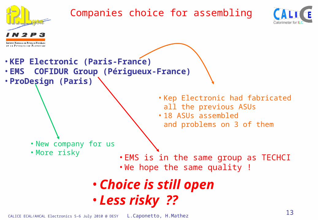
Companies choice for assembling
•KEP Electronic (Paris-France)•EMS COFIDUR Group (Périgueux-France)•ProDesign (Paris)
• Kep Electronic had fabricated all the previous ASUs
• 18 ASUs assembled and problems on 3 of them
• New company for us• More risky •EMS is in the same group as TECHCI
•We hope the same quality !
•Choice is still open•Less risky ??

CALICE ECAL/AHCAL Electronics 5-6 July 2010 @ DESY L.Caponetto, H.Mathez 14
Planning
Aggressive planning :
• 6 ASUs return from Fab on 14 or 21 of July (3 weeks after purchase order)
• 2 ASU to ASU PCB (5 weeks after purchase order)
• 2 DIFF to ASU (3 weeks after purchase order)
• 2 ASUs + Interconnect assembling in few days !!!• Testing before the end of July• Send purchase order for the whole production before vacation
More realistic planning :
• 6 ASUs return fron Fab by the end of July• 2 ASU to ASU PCB • 2 DIFF to ASU• 2 ASUs + Interconnect assembling during August• Testing : beginning of September
CALICE ECAL/AHCAL Electronics 5-6 July 2010 @ DESY L.Caponetto, H.Mathez 15
Trig_ext (Lemo1)
Enable Acq
Enable PP
Vth2
Power On
Power Off
50 µs
Enable PP
Vref -G.R.I
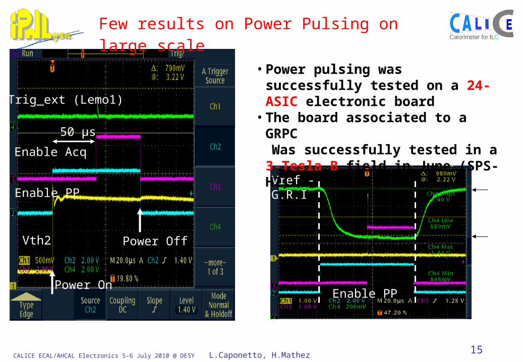
• Power pulsing was successfully tested on a 24-ASIC electronic board
• The board associated to a GRPC Was successfully tested in a 3-Tesla
B field in June (SPS-H2)
Few results on Power Pulsing on large scale
CALICE ECAL/AHCAL Electronics 5-6 July 2010 @ DESY L.Caponetto, H.Mathez 16
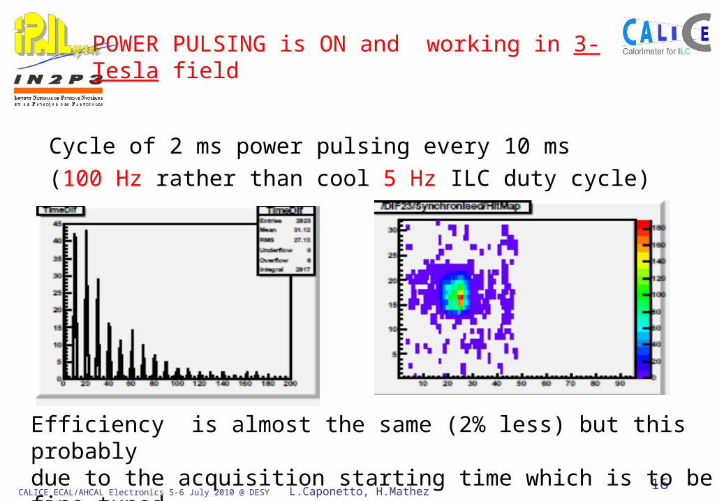
POWER PULSING is ON and working in 3-Tesla field
Cycle of 2 ms power pulsing every 10 ms
(100 Hz rather than cool 5 Hz ILC duty cycle)
Efficiency is almost the same (2% less) but this probablydue to the acquisition starting time which is to be fine-tuned.
CALICE ECAL/AHCAL Electronics 5-6 July 2010 @ DESY L.Caponetto, H.Mathez 17
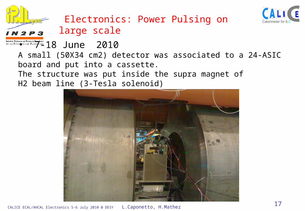
• 7-18 June 2010 A small (50X34 cm2) detector was associated to a 24-ASIC board and put into a cassette.The structure was put inside the supra magnet of H2 beam line (3-Tesla solenoid)
Electronics: Power Pulsing on large scale
CALICE ECAL/AHCAL Electronics 5-6 July 2010 @ DESY L.Caponetto, H.Mathez 18
Conclusion
ASU_V3• Mechatronic
• Modified Connector (Samtek , Kyocera)• Added DIF to ASU board• Added ASU to ASU board• Added holes for 1 sqm assembly
• Electrical modifications to reduce power supply• LVDS buffers with enable • “Select” pin implementation
• Time to manufacturing increase due to this main modifications :(2 months)
• Technical study with TECHCI • before mass production• Delocalization required more detailed
fabrication data exchange with TECHCI
•Test bench for HR production characterization : in progress