Embed Size (px)
Citation preview
IOSR Journal of Electronics and Communication Engineering (IOSR-JECE)
e-ISSN: 2278-2834,p- ISSN: 2278-8735.Volume 10, Issue 1, Ver. 1 (Jan - Feb. 2015), PP 15-19 www.iosrjournals.org
DOI: 10.9790/2834-10111519 www.iosrjournals.org 15 | Page
Canny Edge Detection Algorithm on FPGA
1Malathy H Lohithaswa
Abstract: Edge detection is one of the most commonly used operations in image analysis particularly in the
areas of feature extraction. Edge indicates the boundary between overlapping objects. An edge is the boundary
between an object and the background, hence if the edges are identified accurately in an image all its objects
can be located and basic properties such as area, perimeter and shape of an image can be measured. An edge
can be defined as a set of connected pixels that forms a boundary between two disjoints regions. Edge detection
is basically, a method of segmenting an image into regions of discontinuity. The data of edge detection is very large, so the achievement of high speed of image processing is a difficult task. Field Programmable Gate Array
(FPGA) can overcome this difficult task and it is an effective device to realize real-time parallel processing for
vast amounts of image and video data. The proposed work shows the implementation of Canny Edge detection
algorithm on FPGA.
I. Introduction An image may be defined as a two-dimensional function, where x and y are spatial (plane) coordinates,
and the amplitude of f at any pair of coordinates(x, y) is called the intensity or gray level of the image at that
point. There are two methods available in Image Processing: Analog image processing and Digital image
processing. Analog Image Processing refers to the alteration of image through electrical means. The most
common example is the television image. The television signal is a voltage level which varies in amplitude to
represent brightness through the image. In digital image processing digital computers are used to process the image. It is defined as the subjecting numerical representation of objects to a series of operations in order to
obtain a desired result. A digital image is an array of real numbers represented by a finite number of bits. An
image, f(x,y) defined in the "real world" is considered to be a function of two real variables with f as the
amplitude (brightness) of the image at the real coordinate position (x,y). Digital image is composed of a finite
number of elements, each of which has a particular location and value. These elements are called picture
elements, image elements and pixels. The effect of digitization and pixel representation is shown in Figure 1.1
and Figure1.2 respectively.
Image processing involves changing the nature of an image in order to either improve its pictorial
information for human perception, or render it more suitable for autonomous machine perception.
Figure 1.1: Image representation
Figure 1.2: Pixel representation of given image
Canny edge detection algorithm on FPGA
DOI: 10.9790/2834-10111519 www.iosrjournals.org 16 | Page
1.2 Problem Statement
The problem chosen here is to study the canny edge detection algorithm and implementation of the
design in Verilog HDL and to run the design on Spartan 3E FPGA board. The main aim is to transfer the image data to Visual Display Unit (monitor) through Canny Edge detection algorithm on FPGA and to compare the
software and synthesized hardware algorithm outputs
1.3 Canny Edge Detector
Canny edge detector is optimal edge detection and has advanced algorithm derived from the previous
work of Marr and Hildreth. It provides good image detection, clear response and good localization. It is widely
used in current image processing techniques.
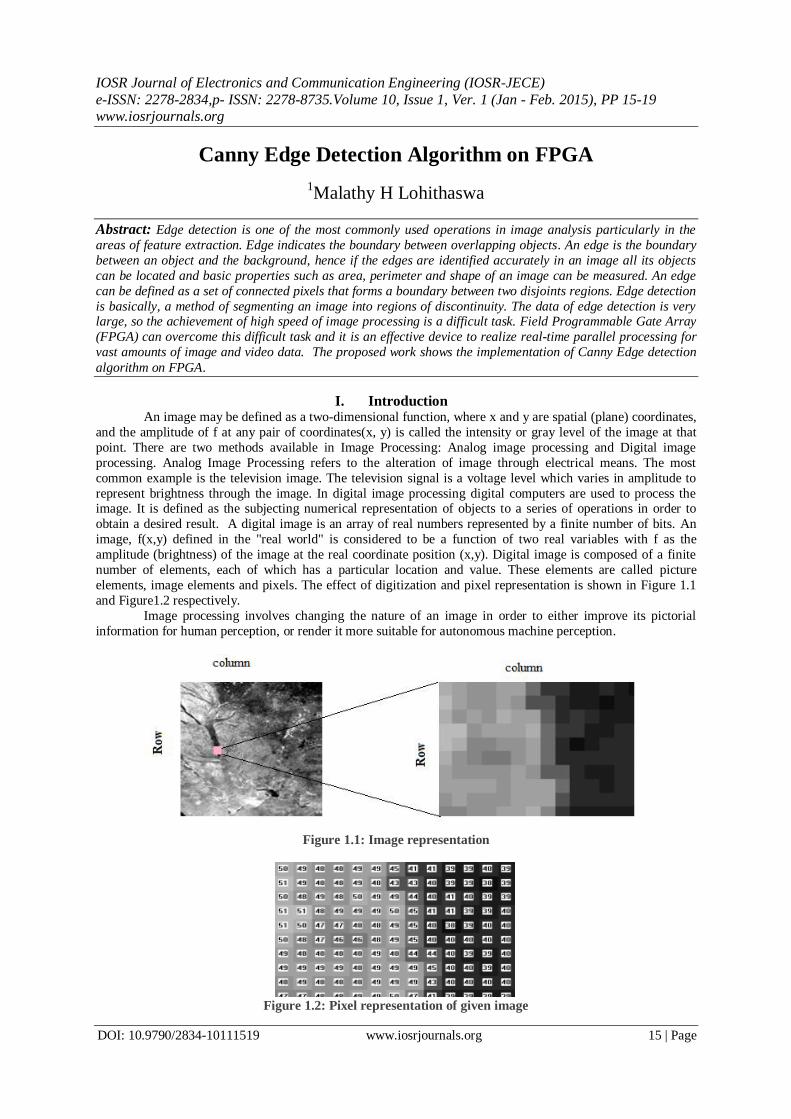
II. High Level Implentation Figure 2.1 Implementation of Canny Edge Detection algorithm is designed using Simulink
From the figure2.1 we can see image from file block which is used to import an image from specified
file. Here the image taken is a static image of M-by-N-by-P array and the block outputs a color image, where M
is the number of rows and N is the number of columns in each color plane, P. Next we have color space
conversion where the color image is converted into gray scale image. Once the image conversion is done it is
passed through an edge detection block where canny edge block is selected and threshold value is set for edge
detection process.
Figure 2.2 Input image converted into gray scale image
Figure 2.3 Edge detected output image of canny edge detector algorithm
Canny edge detection algorithm on FPGA
DOI: 10.9790/2834-10111519 www.iosrjournals.org 17 | Page
There are Pre processing and post processing Block. The pre processing block is used to convert the
two dimensional (2D) image data into one dimensional data and post processing the values are given as the
input to the file block.The Buffer block which converts scalar samples to frame output at lower sampling rate, followed by a 1D to 2D (matrix) format signal block, finally a sink is used to display the output image
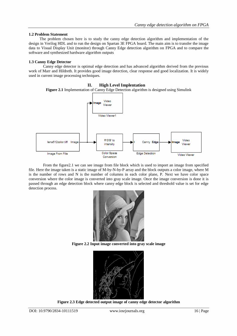
III. Design And Implementation
Figure 3.1: System level block diagram of the entire design
The block diagram of the system level implementation is as shown in the Figure 3.1. The input image
is gray scale image of size 128x128 each pixel of 8 bits wide. The Coefficient (coe) file contains the contents of
the Memory Block for the specified read depth and read width values of the image. The coe file of the input
image is generated using MATLAB. This coe file is loaded into the Block ROM which is then processed using
the Canny edge detection algorithm. The resulting image is displayed on monitor using VGA interfacing.
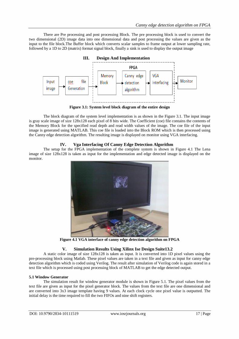
IV. Vga Interfacing Of Canny Edge Detection Algorithm The setup for the FPGA implementation of the complete system is shown in Figure 4.1 The Lena
image of size 128x128 is taken as input for the implementation and edge detected image is displayed on the
monitor.
Figure 4.1 VGA interface of canny edge detection algorithm on FPGA
V. Simulation Results Using Xilinx Ise Design Suite13.2 A static color image of size 128x128 is taken as input. It is converted into 1D pixel values using the
pre-processing block using Matlab. These pixel values are taken in a text file and given as input for canny edge
detection algorithm which is coded using Verilog. The result after simulation of Verilog code is again stored in a text file which is processed using post processing block of MATLAB to get the edge detected output.
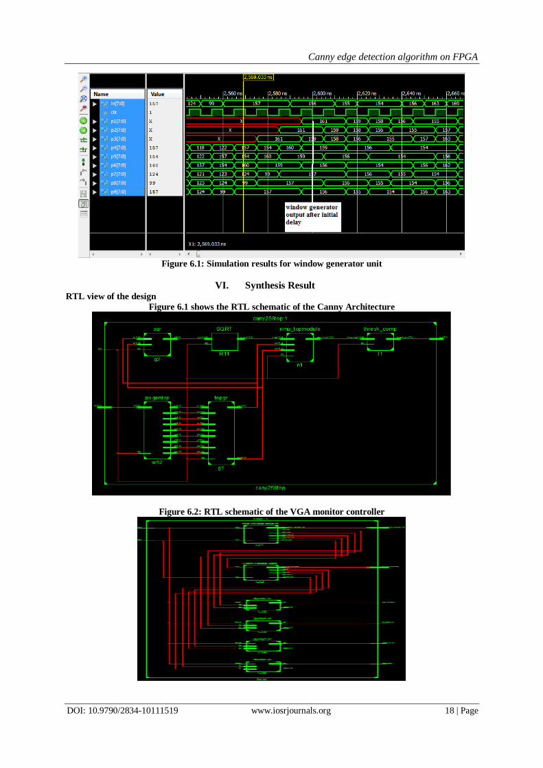
5.1 Window Generator
The simulation result for window generator module is shown in Figure 5.1. The pixel values from the
text file are given as input for the pixel generator block. The values from the text file are one dimensional and
are converted into 3x3 image template having 9 values. At each clock cycle one pixel value is outputted. The
initial delay is the time required to fill the two FIFOs and nine shift registers.
Canny edge detection algorithm on FPGA
DOI: 10.9790/2834-10111519 www.iosrjournals.org 18 | Page
Figure 6.1: Simulation results for window generator unit
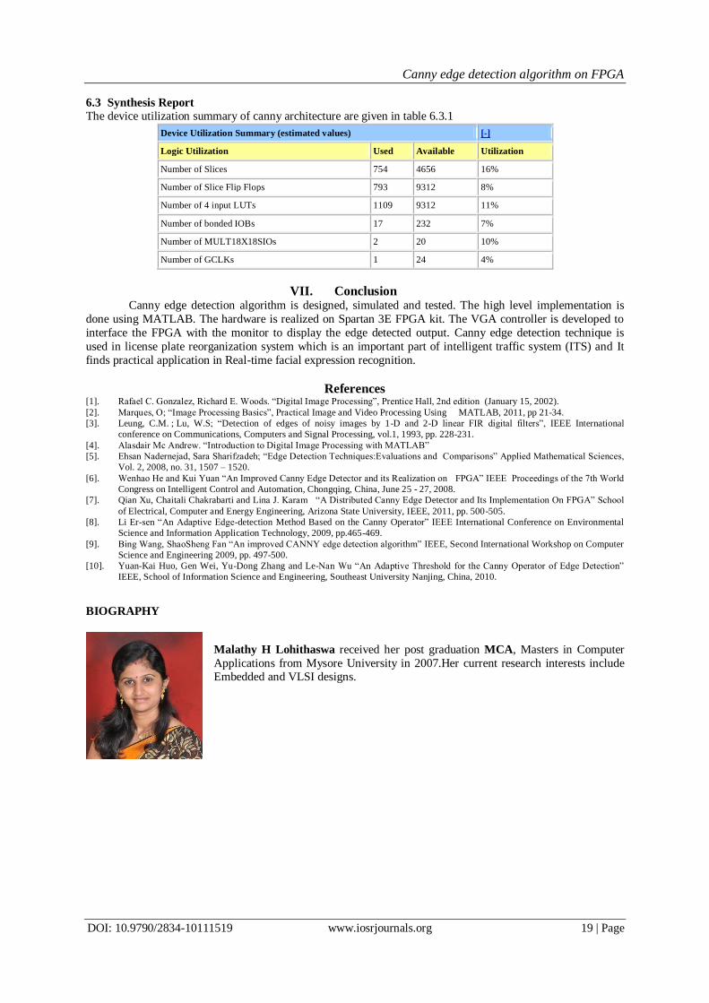
VI. Synthesis Result RTL view of the design
Figure 6.1 shows the RTL schematic of the Canny Architecture
Figure 6.2: RTL schematic of the VGA monitor controller
Canny edge detection algorithm on FPGA
DOI: 10.9790/2834-10111519 www.iosrjournals.org 19 | Page
6.3 Synthesis Report
The device utilization summary of canny architecture are given in table 6.3.1
Device Utilization Summary (estimated values) [-]
Logic Utilization Used Available Utilization
Number of Slices 754 4656 16%
Number of Slice Flip Flops 793 9312 8%
Number of 4 input LUTs 1109 9312 11%
Number of bonded IOBs 17 232 7%
Number of MULT18X18SIOs 2 20 10%
Number of GCLKs 1 24 4%
VII. Conclusion Canny edge detection algorithm is designed, simulated and tested. The high level implementation is
done using MATLAB. The hardware is realized on Spartan 3E FPGA kit. The VGA controller is developed to
interface the FPGA with the monitor to display the edge detected output. Canny edge detection technique is
used in license plate reorganization system which is an important part of intelligent traffic system (ITS) and It
finds practical application in Real-time facial expression recognition.
References [1]. Rafael C. Gonzalez, Richard E. Woods. “Digital Image Processing”, Prentice Hall, 2nd edition (January 15, 2002).
[2]. Marques, O; “Image Processing Basics”, Practical Image and Video Processing Using MATLAB, 2011, pp 21-34.
[3]. Leung, C.M. ; Lu, W.S; “Detection of edges of noisy images by 1-D and 2-D linear FIR digital filters”, IEEE International
conference on Communications, Computers and Signal Processing, vol.1, 1993, pp. 228-231.
[4]. Alasdair Mc Andrew. “Introduction to Digital Image Processing with MATLAB”
[5]. Ehsan Nadernejad, Sara Sharifzadeh; “Edge Detection Techniques:Evaluations and Comparisons” Applied Mathematical Sciences,
Vol. 2, 2008, no. 31, 1507 – 1520.
[6]. Wenhao He and Kui Yuan “An Improved Canny Edge Detector and its Realization on FPGA” IEEE Proceedings of the 7th World
Congress on Intelligent Control and Automation, Chongqing, China, June 25 - 27, 2008.
[7]. Qian Xu, Chaitali Chakrabarti and Lina J. Karam “A Distributed Canny Edge Detector and Its Implementation On FPGA” School
of Electrical, Computer and Energy Engineering, Arizona State University, IEEE, 2011, pp. 500-505.
[8]. Li Er-sen “An Adaptive Edge-detection Method Based on the Canny Operator” IEEE International Conference on Environmental
Science and Information Application Technology, 2009, pp.465-469.
[9]. Bing Wang, ShaoSheng Fan “An improved CANNY edge detection algorithm” IEEE, Second International Workshop on Computer
Science and Engineering 2009, pp. 497-500.
[10]. Yuan-Kai Huo, Gen Wei, Yu-Dong Zhang and Le-Nan Wu “An Adaptive Threshold for the Canny Operator of Edge Detection”
IEEE, School of Information Science and Engineering, Southeast University Nanjing, China, 2010.
BIOGRAPHY
Malathy H Lohithaswa received her post graduation MCA, Masters in Computer
Applications from Mysore University in 2007.Her current research interests include Embedded and VLSI designs.


![Canny Edge Detection on NVIDIA CUDAusers.umiacs.umd.edu/~ramani/pubs/luo_gpu_canny_fin_2008.pdf · Canny edge detector [3]. This algorithm has remained a standard in edge finding](https://img.pdfslide.net/doc/110x75/5ec99bcd02f2c14ba77679b2/canny-edge-detection-on-nvidia-ramanipubsluogpucannyfin2008pdf-canny-edge.jpg)
![HARDWARE REALIZATION OF CANNY EDGE DETECTION ALGORITHM …jestec.taylors.edu.my/Vol 12 issue 9 September 2017/12_9_19.pdf · detector [16, 17]. Canny edge detector is recognized as](https://img.pdfslide.net/doc/110x75/5ec997e30faed455df46e742/hardware-realization-of-canny-edge-detection-algorithm-12-issue-9-september-201712919pdf.jpg)