Embed Size (px)
Citation preview

Capacitance of Silicon Pixels
Sally Seidel, Grant Gorfine, Martin Hoeferkamp,
Veronica Mata-Bruni, and Geno Santistevan
University of New Mexico
PIXEL 2000 Conference
5 June 2000
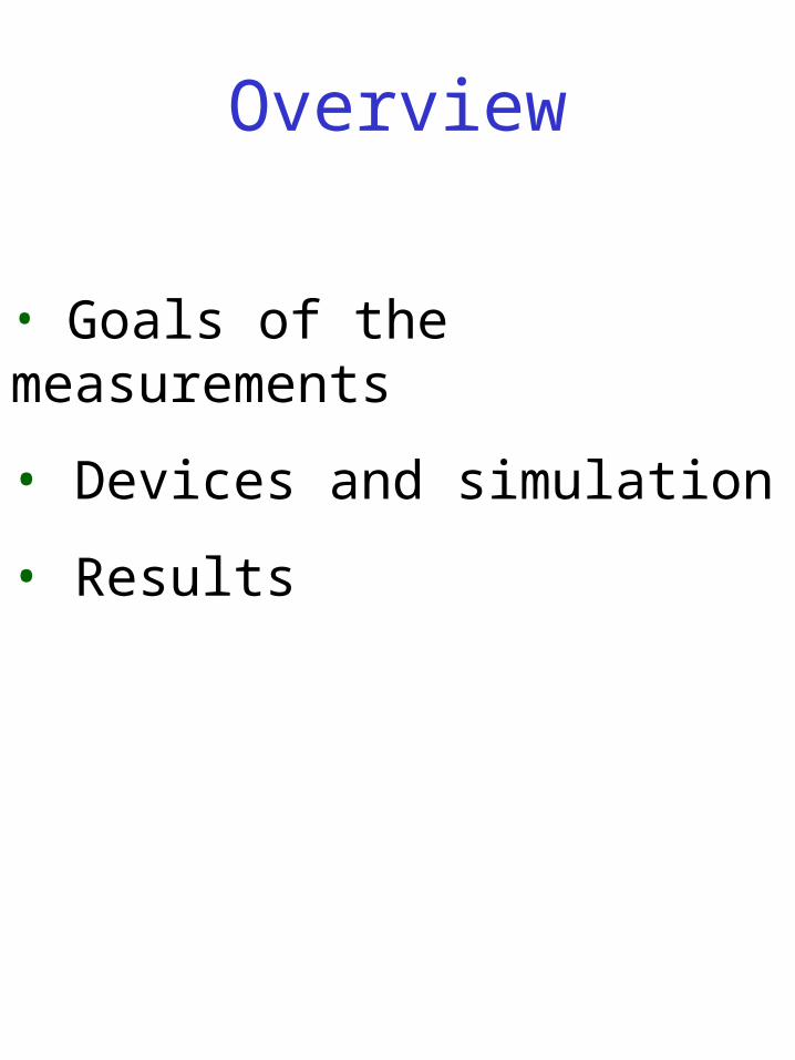
Overview
• Goals of the measurements
• Devices and simulation
• Results
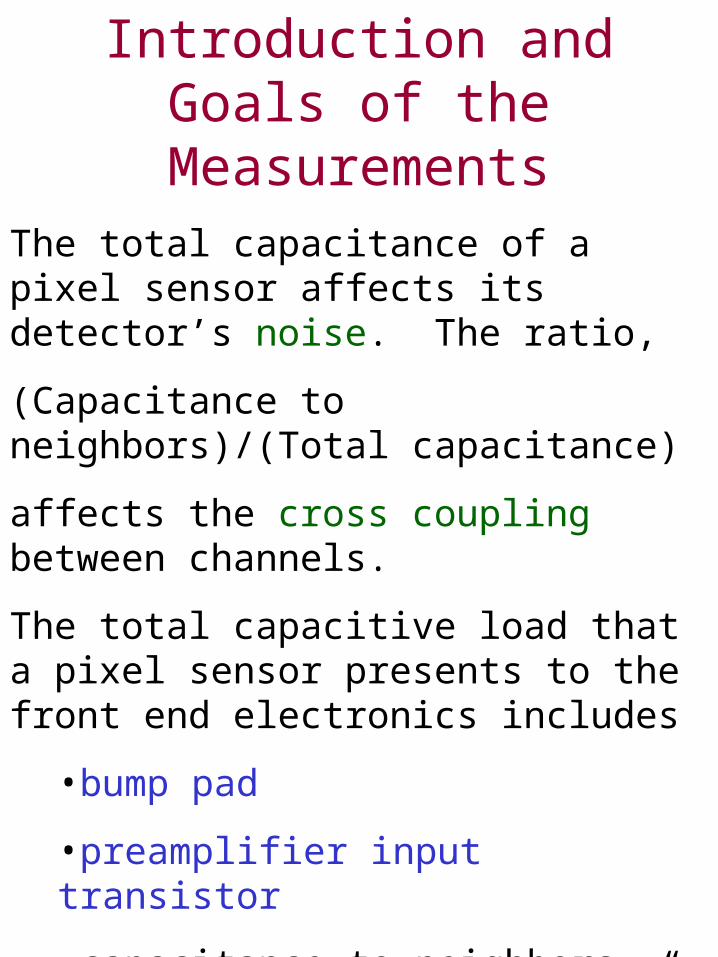
Introduction and Goals of the Measurements
The total capacitance of a pixel sensor affects its detector’s noise. The ratio,
(Capacitance to neighbors)/(Total capacitance)
affects the cross coupling between channels.
The total capacitive load that a pixel sensor presents to the front end electronics includes
•bump pad
•preamplifier input transistor
•capacitance to neighbors (“inter-pixel contribution”)
•backplane contribution
This study examines inter-pixel + backplane capacitance.
For application to LHC + Tevatron experiments, we include the effects of
•radiation damage and
•low temperature operation.
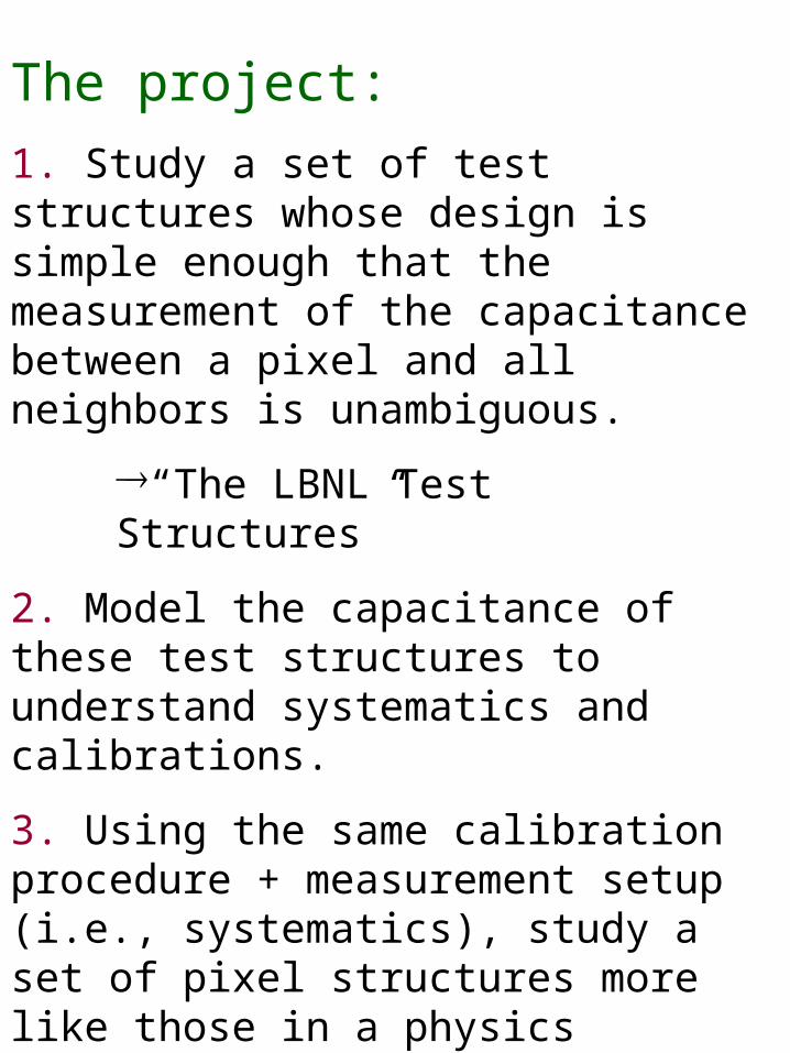
The project:
1. Study a set of test structures whose design is simple enough that the measurement of the capacitance between a pixel and all neighbors is unambiguous.
“The LBNL Test Structures”
2. Model the capacitance of these test structures to understand systematics and calibrations.
3. Using the same calibration procedure + measurement setup (i.e., systematics), study a set of pixel structures more like those in a physics detector. These sensors use p-stop isolation.
“Structure 6”
4. Measure the inter-pixel and backplane capacitance of ATLAS prototype (p-spray) sensors.
5. Investigate the dependence of the capacitance on operating temperature.
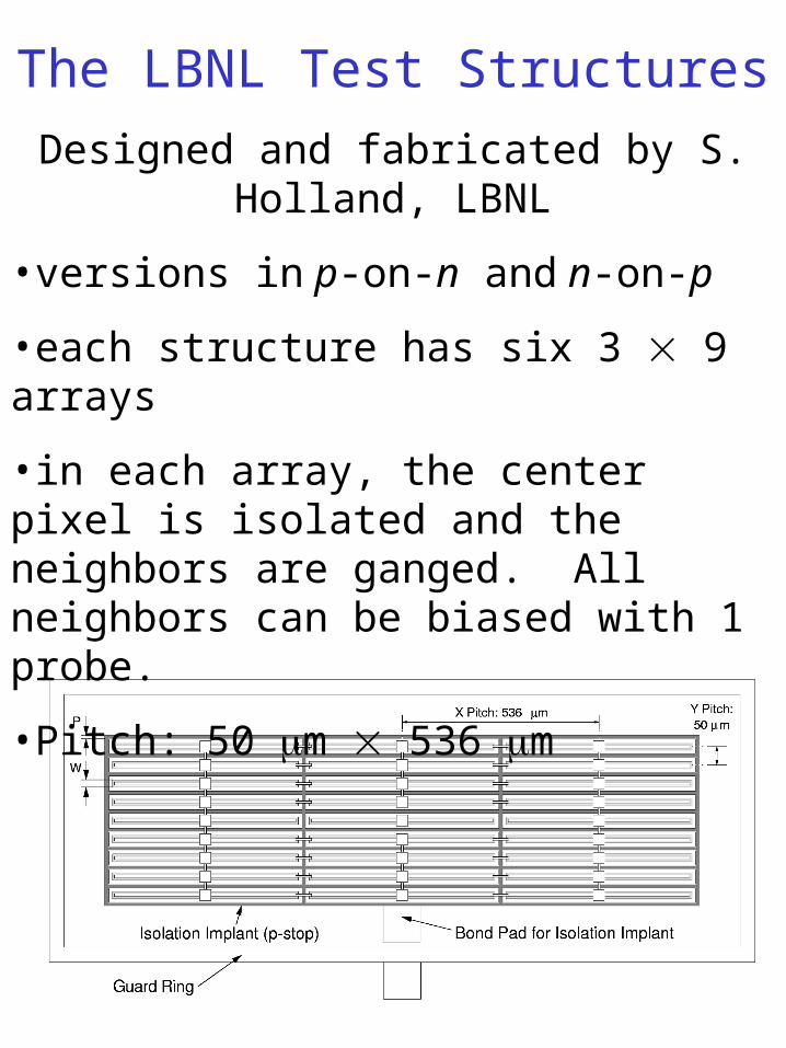
The LBNL Test Structures
Designed and fabricated by S. Holland, LBNL
•versions in p-on-n and n-on-p
•each structure has six 3 9 arrays
•in each array, the center pixel is isolated and the neighbors are ganged. All neighbors can be biased with 1 probe.
•Pitch: 50 m 536 m
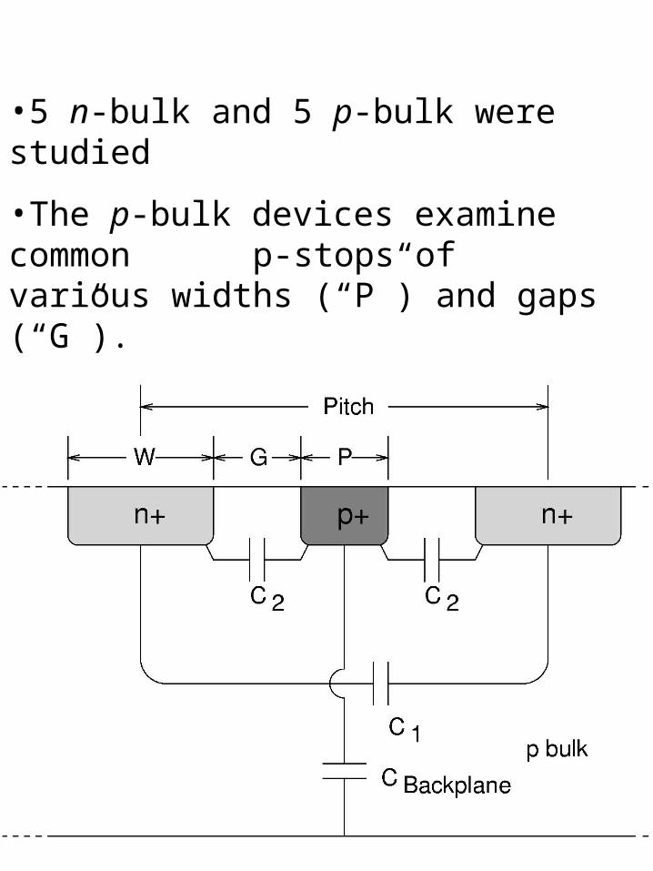
•5 n-bulk and 5 p-bulk were studied
•The p-bulk devices examine common p-stops of various widths (“P”) and gaps (“G”).
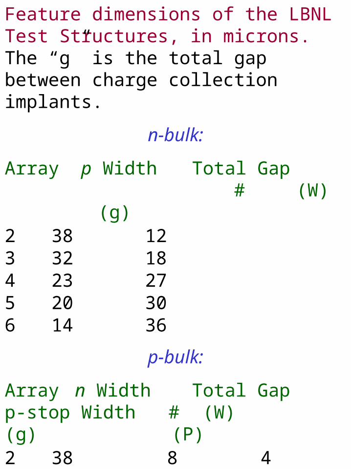
Feature dimensions of the LBNL Test Structures, in microns. The “g” is the total gap between charge collection implants.
n-bulk:
Array p Width Total Gap # (W) (g) 2 38 123 32 184 23 275 20 306 14 36
p-bulk:
Array n Width Total Gap p-stop Width # (W) (g) (P)2 38 8 43 32 12 64 23 19 85 20 20 106 14 24 12
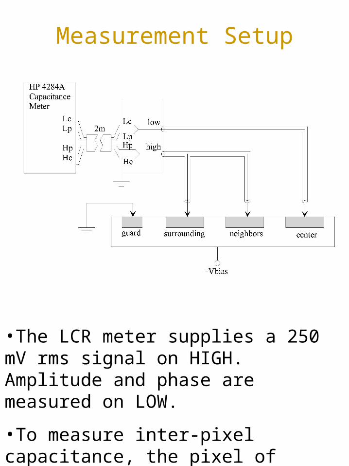
Measurement Setup
•The LCR meter supplies a 250 mV rms signal on HIGH. Amplitude and phase are measured on LOW.
•To measure inter-pixel capacitance, the pixel of interest is connected to LOW, all others to HIGH.
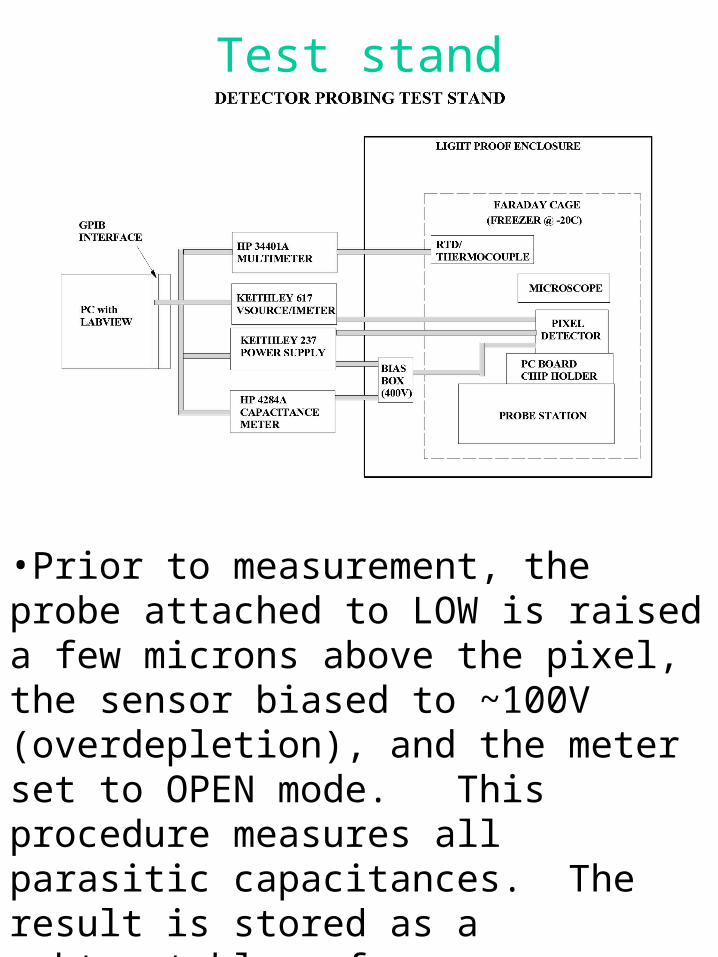
Test stand
•Prior to measurement, the probe attached to LOW is raised a few microns above the pixel, the sensor biased to ~100V (overdepletion), and the meter set to OPEN mode. This procedure measures all parasitic capacitances. The result is stored as a subtractable reference.
•Residual parasitic capacitance after OPEN correction: < 2 fF.
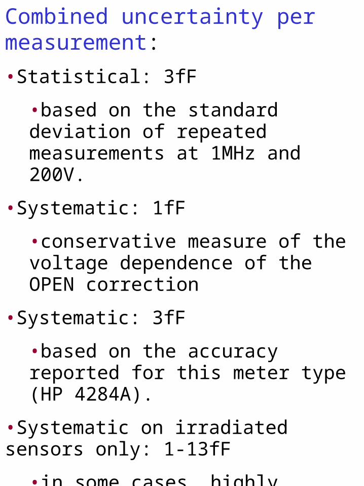
Combined uncertainty per measurement:
•Statistical: 3fF
•based on the standard deviation of repeated measurements at 1MHz and 200V.
•Systematic: 1fF
•conservative measure of the voltage dependence of the OPEN correction
•Systematic: 3fF
•based on the accuracy reported for this meter type (HP 4284A).
•Systematic on irradiated sensors only: 1-13fF
•in some cases, highly irradiated sensors risked thermal runaway if operated at room temperature at voltages required to plateau their Cinter-pixel-V curve. For them, the minimum Cinter-pixel was determined by extrapolation.
LBNL Test Structure Measurement Results:
•for p-on-n and n-on-p
•for frequencies of 3 kHz, 10 kHz, 100 kHz, and 1 MHz
•unirradiated and after 4.8 x 1013 cm-2 (1 MeV neutron equivalent) fluence
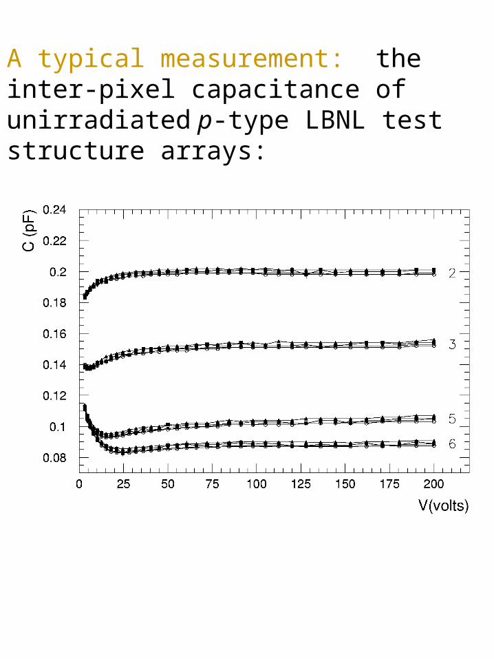
A typical measurement: the inter-pixel capacitance of unirradiated p-type LBNL test structure arrays:
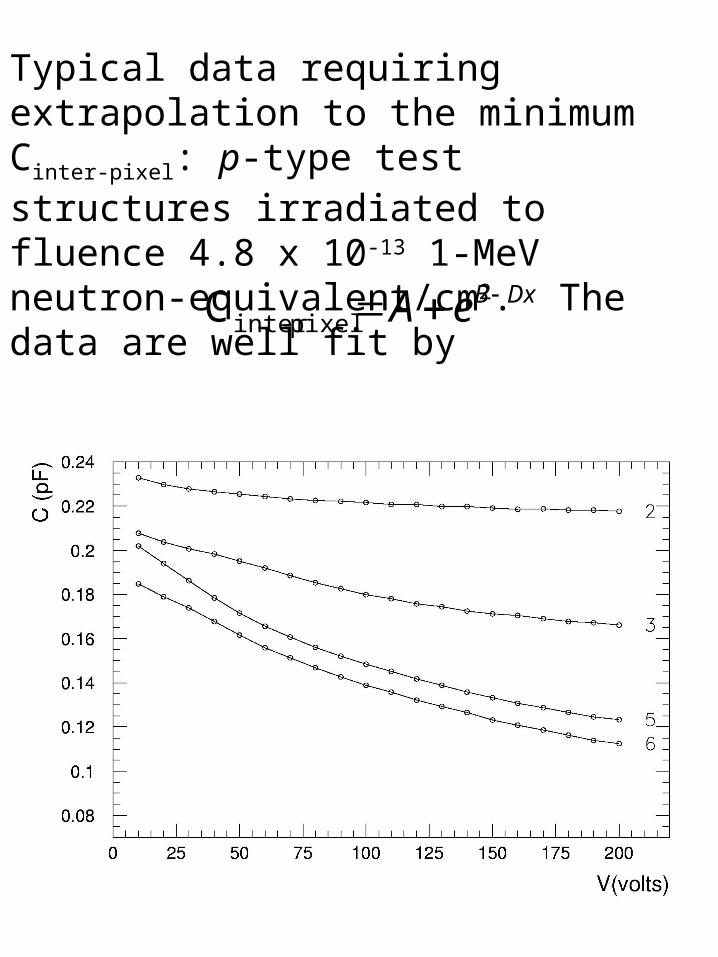
Typical data requiring extrapolation to the minimum Cinter-pixel: p-type test structures irradiated to fluence 4.8 x 10⁻¹³ 1-MeV neutron-equivalent/cm2. The data are well fit by
DxBeA pixel-interC
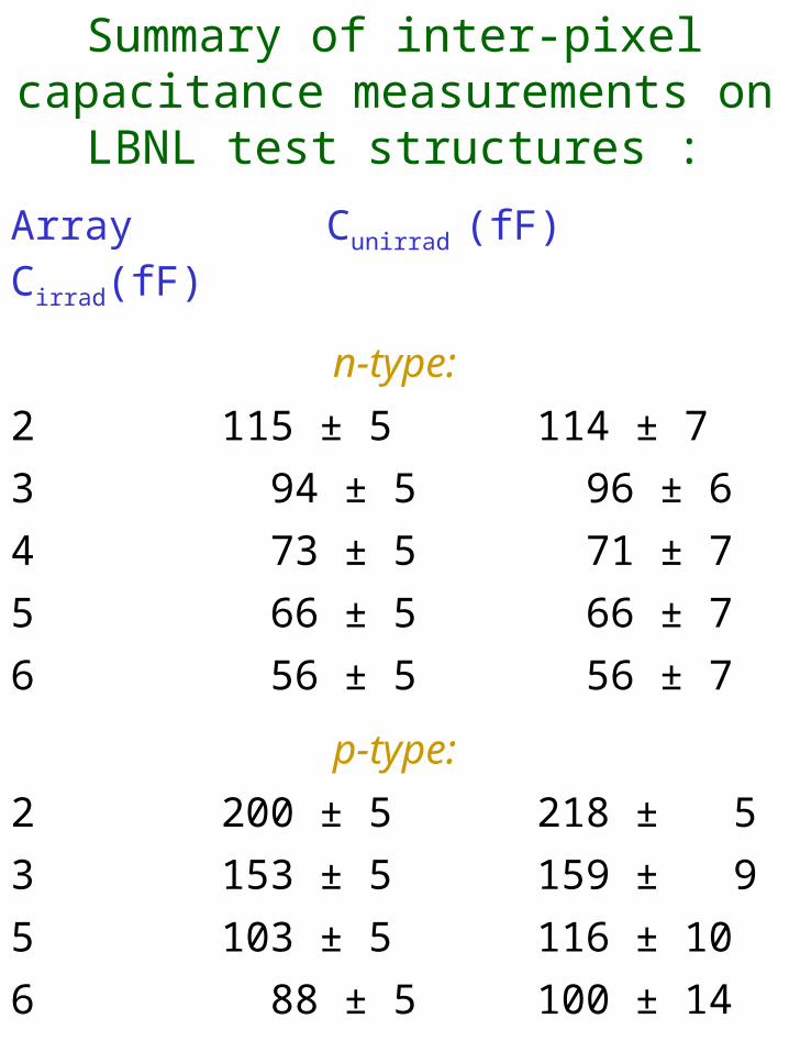
Summary of inter-pixel capacitance measurements on LBNL test structures :
Array Cunirrad (fF) Cirrad(fF)
n-type:
2 115 ± 5 114 ± 7
3 94 ± 5 96 ± 6
4 73 ± 5 71 ± 7
5 66 ± 5 66 ± 7
6 56 ± 5 56 ± 7
p-type:
2 200 ± 5 218 ± 5
3 153 ± 5 159 ± 9
5 103 ± 5 116 ± 10
6 88 ± 5 100 ± 14
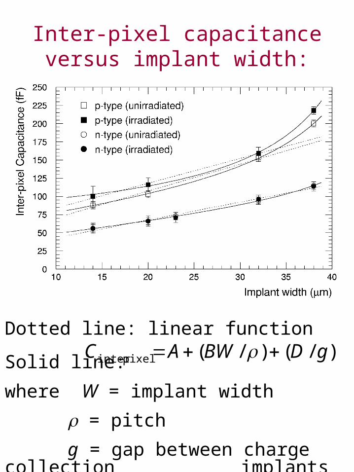
Inter-pixel capacitance versus implant width:
Dotted line: linear function
Solid line:
where W = implant width
= pitch
g = gap between charge collection implants
),/()/(pixel-inter gDBWAC
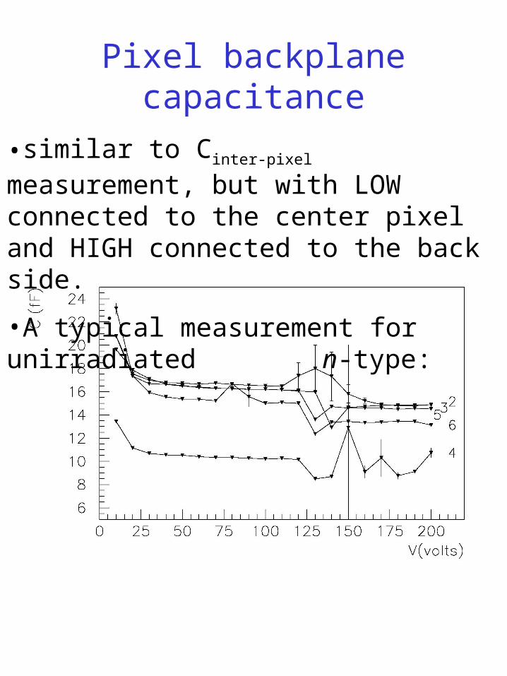
Pixel backplane capacitance
•similar to Cinter-pixel measurement, but with LOW connected to the center pixel and HIGH connected to the back side.
•A typical measurement for unirradiated n-type:
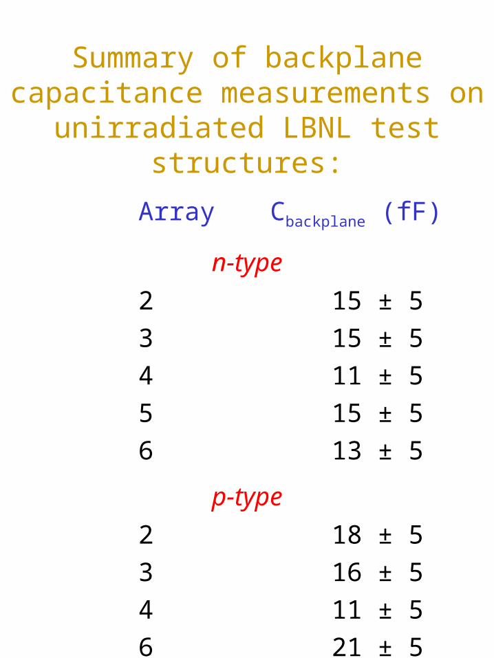
Summary of backplane capacitance measurements on unirradiated LBNL
test structures:
Array Cbackplane (fF)
n-type
2 15 ± 5
3 15 ± 5
4 11 ± 5
5 15 ± 5
6 13 ± 5
p-type
2 18 ± 5
3 16 ± 5
4 11 ± 5
6 21 ± 5
Simulation of the LBNL Test Structures
•Results of 2-D simulators HSPICE and IES Electro and 3-D simulator IES Coulomb were compared to interpret the measurements, indicate the precision of simulation, and estimate the size of contribution of non-adjacent neighbors.
•The simulators take as input the geometry of the sensor and information about the dielectrics and solve the electrostatic field equations.
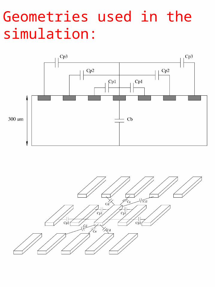
Geometries used in the simulation:
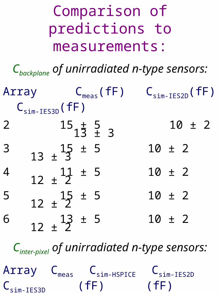
Comparison of predictions to measurements:
Cbackplane of unirradiated n-type sensors:
Array Cmeas(fF) Csim-IES2D(fF) Csim-IES3D(fF)
2 15 ± 5 10 ± 2 13 ± 33 15 ± 5 10 ± 2 13 ± 34 11 ± 5 10 ± 2 12 ± 25 15 ± 5 10 ± 2 12 ± 26 13 ± 5 10 ± 2 12 ± 2
Cinter-pixel of unirradiated n-type sensors:
Array Cmeas Csim-HSPICE Csim-IES2D Csim-IES3D
(fF) (fF) (fF) (fF)
2 115±5 130±46 109±38 124±433 94±5 115±40 91±32 111±394 73±5 95±32 78±27 93±335 66±5 89±31 72±25 87±306 56±5 75±26 66±23 76±27
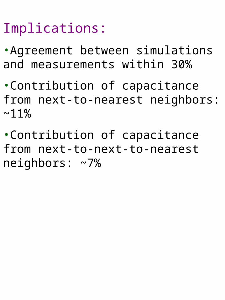
Implications:
•Agreement between simulations and measurements within 30%
•Contribution of capacitance from next-to-nearest neighbors: ~11%
•Contribution of capacitance from next-to-next-to-nearest neighbors: ~7%
Implications of the LBNL Test Structure studies:
•good agreement between measurement and simulation suggests that the measurement procedure may be used for values in the range 10 fF - a few hundred fF.
•For sensors with 50 m pitch, 300m thickness, typical ratio Cbackplane/Cinter-pixel is 10-25%.
We next apply the procedure to a set of more realistic pixel arrays, Structure 6...
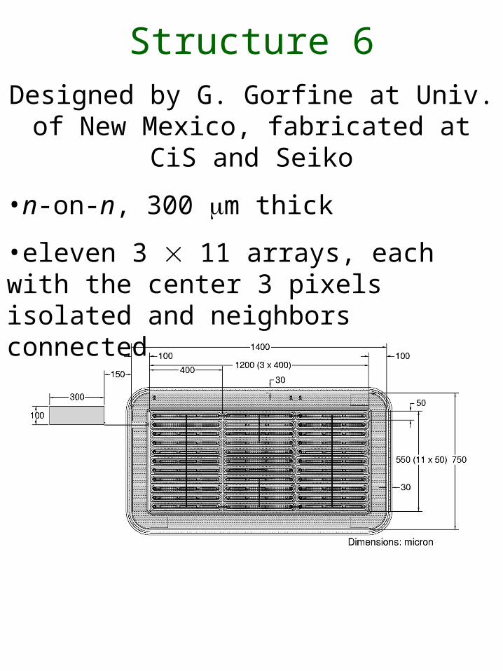
Structure 6Designed by G. Gorfine at Univ. of New
Mexico, fabricated at CiS and Seiko
•n-on-n, 300 m thick
•eleven 3 11 arrays, each with the center 3 pixels isolated and neighbors connected
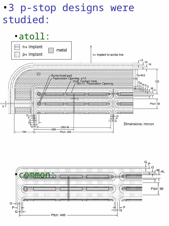
•3 p-stop designs were studied:
•atoll:
•common:
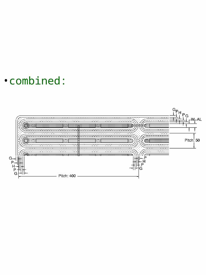
•combined:
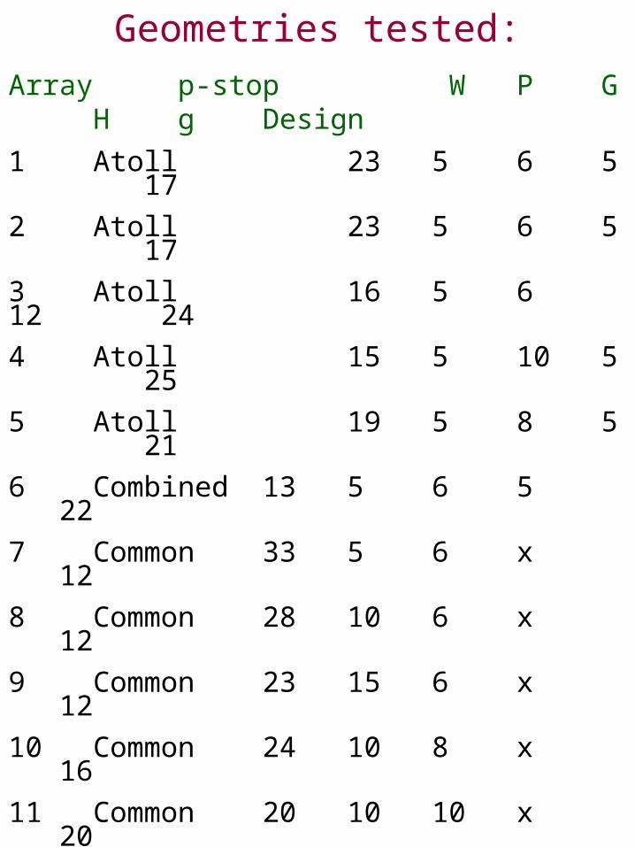
Geometries tested:
Array p-stop W P G H gDesign
1 Atoll 23 5 6 5 17
2 Atoll 23 5 6 5 17
3 Atoll 16 5 6 12 24
4 Atoll 15 5 10 5 25
5 Atoll 19 5 8 5 21
6 Combined 13 5 6 5 22
7 Common 33 5 6 x 12
8 Common 28 10 6 x 12
9 Common 23 15 6 x 12
10 Common 24 10 8 x 16
11 Common 20 10 10 x 20
W = n-implant widthP = p-stop widthG = gap between n- and p-implantsH = gap between neighboring p-implantsg = total gap between charge collection implantsAll arrays except #2 have metal narrower than implant.
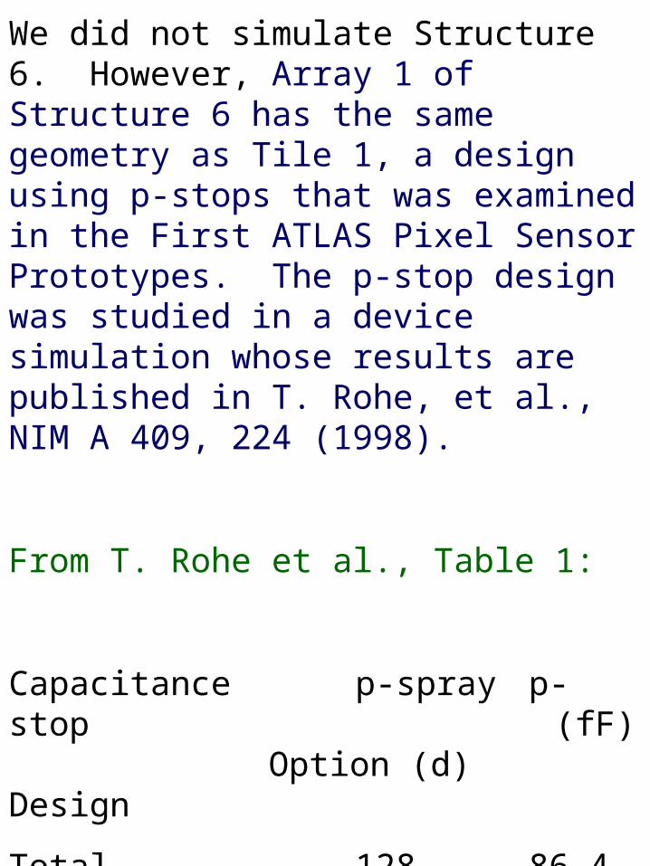
We did not simulate Structure 6. However, Array 1 of Structure 6 has the same geometry as Tile 1, a design using p-stops that was examined in the First ATLAS Pixel Sensor Prototypes. The p-stop design was studied in a device simulation whose results are published in T. Rohe, et al., NIM A 409, 224 (1998).
From T. Rohe et al., Table 1:
Capacitance p-spray p-stop (fF) Option (d) Design
Total 128 86.4
1st neighbor 54.0 33.0
2nd neighbor 3.96 3.6
Backplane 7.35 7.4
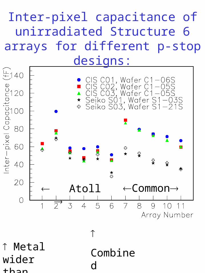
Inter-pixel capacitance of unirradiated Structure 6 arrays for different p-stop
designs:
Atoll Common
Combined
Metal wider than implant
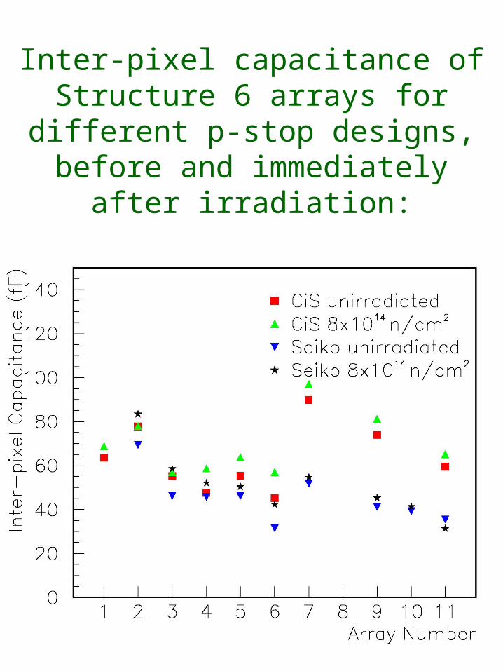
Inter-pixel capacitance of Structure 6 arrays for different p-stop designs,
before and immediately after irradiation:
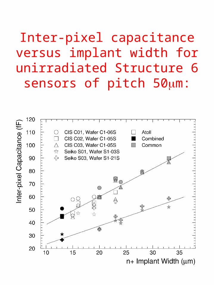
Inter-pixel capacitance versus implant width for unirradiated Structure 6
sensors of pitch 50m:
We next apply the procedure to the ATLAS prototype pixel sensors with p-spray* isolation…
*R. H. Richter et al., NIM A 377, 412 (1996).
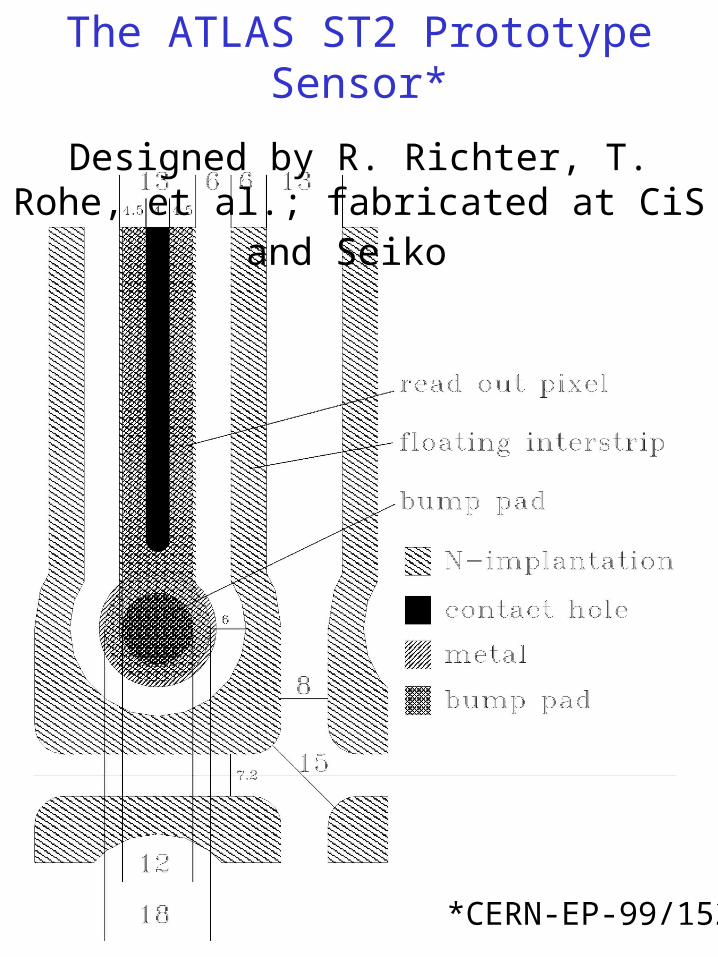
The ATLAS ST2 Prototype Sensor*
Designed by R. Richter, T. Rohe, et al.; fabricated at CiS and Seiko
*CERN-EP-99/152
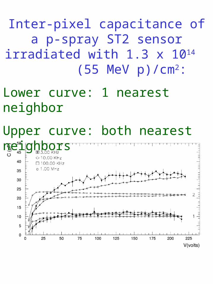
Inter-pixel capacitance of a p-spray ST2 sensor irradiated with 1.3 x 10¹⁴ (55
MeV p)/cm2:
Lower curve: 1 nearest neighbor
Upper curve: both nearest neighbors
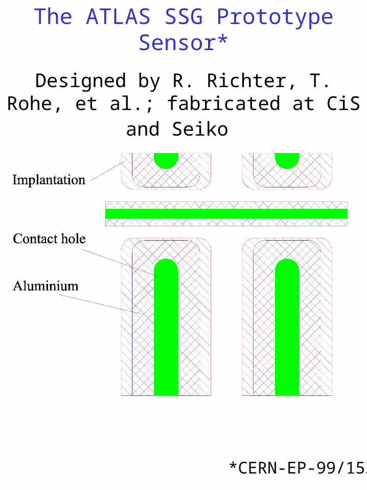
The ATLAS SSG Prototype Sensor*
Designed by R. Richter, T. Rohe, et al.; fabricated at CiS and Seiko
*CERN-EP-99/152
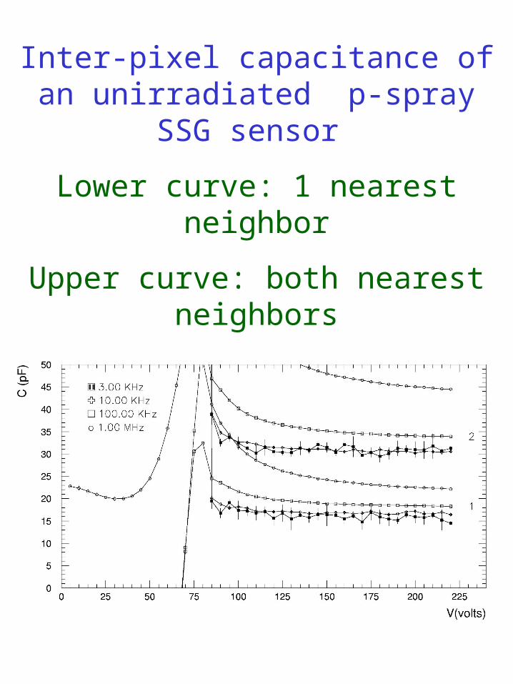
Inter-pixel capacitance of an unirradiated p-spray SSG sensor
Lower curve: 1 nearest neighbor
Upper curve: both nearest neighbors
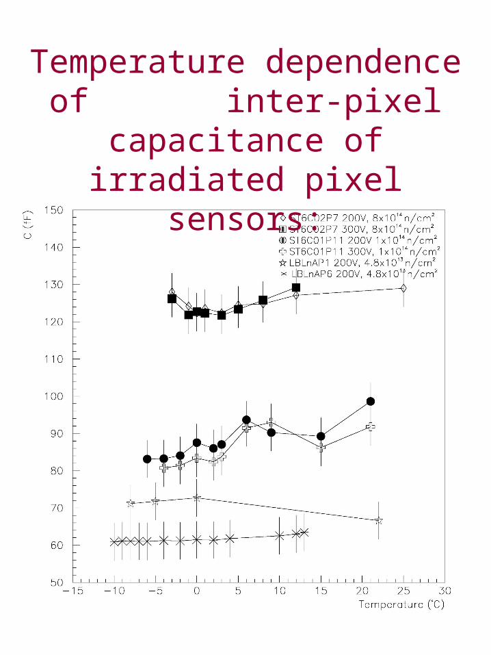
Temperature dependence of inter-pixel capacitance of irradiated
pixel sensors: