Embed Size (px)
Citation preview

©2003 by Elsevier Science (USA).From The System Designer's Guide to VHDL-AMS, by Peter J. Ashenden, Greg D. Peterson and Darrell A. Teegarden.
18chapter eighteen
Case Study 3:DC-DC Power Converter
With a contribution by Tom Egel,Mentor Graphics Corporation
This case study illustrates how VHDL-AMS can be
used for the detailed design of a DC-DC switching
power supply. For the RC airplane system, a step-
down converter is required to convert the 42 V bat-
tery voltage used to power the propeller motor to the
4.8 V needed for the on-board servo electronics. In
this case study we briefly introduce switched-mode
power supply theory, and then perform a detailed
design of a simple step-down (buck) converter. We
discuss averaging techniques that facilitate analy-
sis of the closed-loop system and use VHDL-AMS
simulations to perform system-level design trade-
offs.

558 chapter eighteen Case Study 3: DC-DC Power Converter
©2003 by Elsevier Science (USA).From The System Designer's Guide to VHDL-AMS, by Peter J. Ashenden, Greg D. Peterson and Darrell A. Teegarden.
18.1 Buck Converter Theory and Design
In this case study, we examine the design of a switching power converter for the RCairplane, outlined in Figure 18-1. Switch-mode power supplies have all but replacedtheir linear counterparts as the preferred method for converting the supply of DCpower from one voltage level to another. This is especially true in today’s world ofhandheld compact electronic systems, where size, weight, efficiency and cost are allcritical to the overall system design. All switching supplies use pulse-width modula-tion (PWM) techniques to achieve efficiency and provide the necessary control of theoutput voltage as load conditions change. Because of the combination of electronicand magnetic components in a switching power supply, computer simulation plays avital role in creating a successful design. As we will see, VHDL-AMS is well suited tohandle both this mixed-technology aspect and the state-averaging techniques com-monly used for the design and analysis of switch-mode power supply systems. For amore complete study on switching power converter theory and design, see Brown [7].
Selecting a Switching Regulator Topology
There are two basic types of PWM switching regulators: forward mode and flybackmode. From these two basic modes, the common topologies are formed. The buck(step-down) converter is a forward-mode converter, whereas the boost (step-up) andthe buck-boost (step-up/down) are derivations of the flyback-mode converter. All ofthese converters have the same four basic elements: a power switch for creating thePWM control waveform, a diode, an inductor and a capacitor. The duty cycle of the
FIGURE 18-1
The RC airplane system with the switching power converter outlined.
– +Battery(42 V)
Amp
Throttle AmpMotor/Propeller
Control Stick Analog to Bitstream
Bitstream to Pulse-Width Pulse-Width to Analog
RF Transmit/Receive
Buck Converter
s+as+b
Rudder Servo and Amp
DC
DCMotor/Rudder
Assembly
18.1 Buck Converter Theory and Design 559
©2003 by Elsevier Science (USA).From The System Designer's Guide to VHDL-AMS, by Peter J. Ashenden, Greg D. Peterson and Darrell A. Teegarden.
switch control signal determines how long the switch is closed during any given pe-riod and thus can be used to control the amount of energy stored in the inductor. Acomplete switching power supply also includes a transformer to provide isolation be-tween the input and output and feedback to control the duty cycle of the PWM wave-form as load conditions change.
The requirements of our regulator design are shown in Figure 18-2. They indicatethat we need to convert a 42 V DC battery input to 4.8 V DC. For this we need todesign a forward-mode (buck) converter. The basic topology is shown in Figure 18-3.In the remainder of this section we describe the detailed operation of a buck converterand walk through the design process.
The buck converter shown in Figure 18-3 has two basic modes of operation: con-tinuous mode and discontinuous mode, referring to the current flowing through theinductor (L1). In continuous mode, current is always flowing through L1 whether theswitch (SW1) is on or off, while in discontinuous mode the inductor current goes tozero during part of the off time of SW1. Since the frequency response is significantlydifferent between the two modes, it is best to operate in only one of the modes. Forthis case study, we design the converter to operate only in the continuous mode bysizing the inductor according to the worst-case load conditions to avoid the zero cur-rent threshold. Keeping the buck converter operating in continuous mode also sim-plifies the design and analysis considerably.
FIGURE 18-3
Basic buck converter topology.
FIGURE 18-2
Input Specifications Output Specifications
Vin 42 V DC Vout 4.8 V DC
Fswitching 25 kHz Vout(ripple) < 100 mV p-p
Iout 15 mA to 2 A
Iout(ripple) < 30 mA p-p
Regulator design requirements.
+–DC D1 C1 Rload
L1
SW1
Vin Vmid Vout
Ctrl

560 chapter eighteen Case Study 3: DC-DC Power Converter
©2003 by Elsevier Science (USA).From The System Designer's Guide to VHDL-AMS, by Peter J. Ashenden, Greg D. Peterson and Darrell A. Teegarden.
In continuous mode, the circuit operates in two states: the on state and the offstate, referring to the state of the power switch (SW1) in Figure 18-3. It is commonto draw the equivalent circuit for each of these states to aid in the understanding andderive the circuit equations. We can deduce the equivalent circuits from the originalcircuit. The diode (D1) in a buck converter circuit is sometimes referred to as a passiveswitch, since it also has an on and off state determined by the circuit conditions. Dur-ing the circuit on state, SW1 is on, D1 is reversed biased (off) and current passesthrough the inductor to the load. During the circuit off state, SW1 is off, and D1 isforward biased (on), maintaining the forward current through L1. The equivalent cir-cuits for the on state and off state are shown in Figure 18-4.
The amount of energy transferred to the load is controlled by the duty cycle ofthe switch control waveform. The duty cycle (D) is defined as
(18-1)
where Ts is the total switching period and Ton is the amount of time the switch is on.The duty cycle can range from 0.0 to 1.0, but typically falls between 0.05 and 0.95 (5%to 95%). From Equation 18-1 we can derive equations for Ton and Toff :
(18-2)
(18-3)
FIGURE 18-4
Equivalent circuits for on and off states.
+–DC C1 Rload
L1Vin VmidRon Vout
D1 C1 Rload
L1Vmid
+ Vd = 0.7
–
Vout
On state
Off state
DTon
Ts
--------=
Ton D Ts×=
Toff 1 D–( ) Ts×=

18.1 Buck Converter Theory and Design 561
©2003 by Elsevier Science (USA).From The System Designer's Guide to VHDL-AMS, by Peter J. Ashenden, Greg D. Peterson and Darrell A. Teegarden.
These times are shown in Figure 18-5, which also shows some representative wave-forms for the buck converter operating in continuous mode at steady state with a dutycycle of about 30%.
From Figure 18-5 we see that when the switch is on (ctrl signal is high), the in-ductor current increases while the diode current is zero. When the switch is off, theinductor current decreases and the diode is conducting.
The first step in designing a switching regulator is to select the duty cycle. Forthe buck converter operating in continuous mode, the following relationship can beused to approximate the duty cycle:
(18-4)
From our specifications we can easily calculate the duty cycle required to give the de-sired output. However, since our desired output is relatively small (4.8 V), we shouldinclude the diode voltage drop in the calculation as follows:
(18-5)
Solving for D, the equation becomes
FIGURE 18-5
Buck converter continuous-mode steady-state waveforms.
Ctrl
Switch current
Diode current
Inductor current
0
1
Ts
Ton Toff
∆IL
Vout Vin D×=
Vout Vin D×( ) Vd–=

562 chapter eighteen Case Study 3: DC-DC Power Converter
©2003 by Elsevier Science (USA).From The System Designer's Guide to VHDL-AMS, by Peter J. Ashenden, Greg D. Peterson and Darrell A. Teegarden.
(18-6)
From Equations 18-2 and 18-3 we can also calculate the on and off time of the controlinput. Recall from the power supply requirements that the switching frequency, fs, is25 kHz. Thus, Ts = 1/fs = 40 µs. Noting that Ts = Ton + Toff and substituting inEquations 18-2 and 18-3:
(18-7)
(18-8)
The next step is to calculate the values for the inductor (L1) and capacitor (C1) in theoutput filter. For the inductor we use the familiar equation
(18-9)
where VL is the voltage across the inductor and IL is the inductor current. The goalhere is to select a minimum value for L1 such that the converter operates in continu-ous mode.
In the output specifications we have a minimum output current of 15 mA. Thisminimum current level also sets the maximum allowed current ripple, . If the rip-ple current exceeds 30 mA peak to peak, the inductor current goes to zero during partof the off time, causing the converter to operate in discontinuous mode. This is illus-trated in Figure 18-6.
FIGURE 18-6
Inductor current for continuous and discontinuous modes.
DVout Vd+
Vin
----------------------- 4.8 0.7+42
--------------------- 0.131= = =
Ton 0.131 40 µs× 5.24 µs= =
Toff 1 0.131–( ) 40 µs× 34.76 µs= =
VL Ltd
dIL× LIL∆t∆
-------×≈=
IL∆
Inductor current(continuous mode)
Inductor current(discontinuous mode)
Time
Time
25 mA
0 mA
30 mA
0 mA

18.1 Buck Converter Theory and Design 563
©2003 by Elsevier Science (USA).From The System Designer's Guide to VHDL-AMS, by Peter J. Ashenden, Greg D. Peterson and Darrell A. Teegarden.
To calculate the minimum inductance to remain in continuous mode, we can re-arrange Equation 18-9 to solve for Lmin:
(18-10)
where Ton is the on time and is the maximum ripple current. Here we haveused the equivalent circuit for the on state shown in Figure 18-4, neglecting the onresistance for the switch. The inductor value calculated guarantees continuous-modeoperation as long as the load current does not exceed 15 mA.
The capacitor controls the amount of ripple voltage on the output. The followingformula can be used to calculate the minimum capacitance for a buck converter:
(18-11)
Using a capacitor value equal to or greater than this value guarantees the ripple volt-age will be below 100 mV. The exact value for the capacitor is not critical and is oftenup to 10 times the minimum calculated value.
The final step is to calculate the minimum and maximum load resistance. Thiscan easily be determined from the load current and voltage specifications:
(18-12)
(18-13)
The RLoad(max) value is critical to ensure the current does not fall below 15 mA andforce the circuit into the discontinuous mode.
This completes the design of the basic buck converter. Figure 18-7 shows a struc-tural VHDL-AMS model of the completed open-loop (no feedback) circuit fromFigure 18-3. The time domain simulation results of the output voltage and inductorcurrent are shown in Figure 18-8. To simulate this circuit, we need models for the
Lmin VLt∆
IL max( )∆--------------------×=
Vin Vout–( )Ton
IL max( )∆--------------------×=
42 4.8–( ) 5.2 µs30 mA----------------×=
6.5 mH=
IL max( )∆
Cmin
Iout∆8 Fs× Vout∆×---------------------------------- 30 mA
8 25 kHz× 100 mV×----------------------------------------------------- 1.5 µF= = =
RLoad min( )Vout
Iout max( )--------------------- 4.8 V
2 A------------- 2.4 Ω= = =
RLoad max( )Vout
Iout min( )-------------------- 4.8 V
15 mA---------------- 320 Ω= = =

564 chapter eighteen Case Study 3: DC-DC Power Converter
©2003 by Elsevier Science (USA).From The System Designer's Guide to VHDL-AMS, by Peter J. Ashenden, Greg D. Peterson and Darrell A. Teegarden.
individual components and a test bench that creates the digital control signal with a13.1% duty cycle (see the exercises at the end of this chapter).
From these results the following measurements verify that the open-loop designmeets the specifications:
• Vout(avg) = 4.76 V
• Vout(ripple) = 50 mV
• Iout(avg) = 1.97 A
• Iout(ripple) = 30 mA
FIGURE 18-7
library ieee; use ieee.std_logic_1164.all;library ieee_proposed; use ieee_proposed.electrical_systems.all;
entity tb_BuckConverter isport ( ctrl : std_logic );
end tb_BuckConverter;
––––––––––––––––––––––––––––––––––––––––––––––––––––
architecture tb_BuckConverter of tb_BuckConverter is
terminal vin : electrical;terminal vmid : electrical;terminal vout : electrical;
begin
L1 : entity work.inductor(ideal)generic map ( ind => 6.5e–3 )port map ( p1 => vmid, p2 => vout );
C1 : entity work.capacitor(ideal)generic map ( cap => 1.5e–6 )port map ( p1 => vout, p2 => electrical_ref );
VinDC : entity work.v_constant(ideal)generic map ( level => 42.0 )port map ( pos => vin, neg => electrical_ref );
RLoad : entity work.resistor(ideal)generic map ( res => 2.4 )port map ( p1 => vout, p2 => electrical_ref );
D1 : entity work.diode(ideal)port map ( p => electrical_ref, n => vmid );
sw1 : entity work.switch_dig(ideal)port map ( sw_state => ctrl, p2 => vmid, p1 => vin );
end architecture tb_BuckConverter;
Structural VHDL-AMS code for a buck converter.

18.2 Modeling with VHDL-AMS 565
©2003 by Elsevier Science (USA).From The System Designer's Guide to VHDL-AMS, by Peter J. Ashenden, Greg D. Peterson and Darrell A. Teegarden.
18.2 Modeling with VHDL-AMS
The next step in the design process is to close the loop and provide compensation toensure stability as the load conditions change. Before doing this, however, we willexamine some of the VHDL-AMS models needed for this design in more detail.
The resistor, capacitor, inductor and diode are elementary electrical componentsthat can be easily modeled using the techniques we saw in Chapter 6. Models writtenin VHDL-AMS can be as detailed as desired, including numerous effects beyond idealbehavior. However, it is good practice to include only as much detail as is necessaryfor the analysis being performed. With VHDL-AMS we can write models with varyingdegrees of detail by creating multiple architectures of an entity. It is important to un-derstand what effects are included in a model (and, equally, what effects are exclud-ed) before using the model in a simulation. This helps us to interpret the simulationresults.
Capacitor Model
In previous chapters, we have seen models of an ideal capacitor using the familiarcurrent-voltage relationship:
(18-14)
FIGURE 18-8
Buck converter open-loop transient simulation results.
4.72
4.74
4.76
4.78
4.80
Vol
tage
(V
)
1.9501.960
1.970
1.980
1.990
2.000
2.010
Cur
rent
(A
)
4.730
1.9680
4.759
1.9975
Vout
i ( L1)
19.88 19.90 19.92 19.96 19.98Time (ms)
C2: 19.962 (dx = 0.035)
C1: 19.927
IC Ctd
dVC×=

566 chapter eighteen Case Study 3: DC-DC Power Converter
©2003 by Elsevier Science (USA).From The System Designer's Guide to VHDL-AMS, by Peter J. Ashenden, Greg D. Peterson and Darrell A. Teegarden.
where IC is the current through the capacitor and VC is the voltage across the capac-itor. For switching power supplies it is often necessary to consider the effect of theequivalent series resistance (ESR). If the ESR is too large, it can introduce an unwant-ed “zero” in the frequency response, which may lead to instability.
We can model this effect in VHDL-AMS by including an additional generic con-stant, r_esr, in the entity declaration and creating an additional architecture, as shownin Figure 18-9. In this model, the capacitor is an open circuit at DC and uses the user-specified initial voltage v_ic, provided the value is other than real'low. This value isthe default value for the generic constant and is used to determine whether initializa-tion is required. During time domain simulation, the voltage across the capacitor isreduced by the voltage drop across the equivalent series resistance. The reduced volt-age is used in the statement representing Equation 18-14.
Ideal Switch Model
In the final switching power-supply design, the switch component will typically be apower bipolar transistor or power MOSFET. In the early design stages, we may nothave determined which particular device to use. However, since we are only using
FIGURE 18-9
library ieee_proposed; use ieee_proposed.electrical_systems.all;
entity capacitor isgeneric ( cap : capacitance;
r_esr : resistance := 0.0;v_ic : voltage := real'low );
port ( terminal p1, p2 : electrical );end entity capacitor;
––––––––––––––––––––––––––––––––––––––––––––––––––––
architecture esr of capacitor is
quantity v across i through p1 to p2;quantity vc : voltage; –– Internal voltage across capacitor
begin
if domain = quiescent_domain and v_ic /= real'low usevc == v_ic;i == 0.0;
elsevc == v – (i * r_esr); i == cap * vc'dot;
end use;
end architecture esr;
Capacitor architecture with equivalent series resistance.
18.2 Modeling with VHDL-AMS 567
©2003 by Elsevier Science (USA).From The System Designer's Guide to VHDL-AMS, by Peter J. Ashenden, Greg D. Peterson and Darrell A. Teegarden.
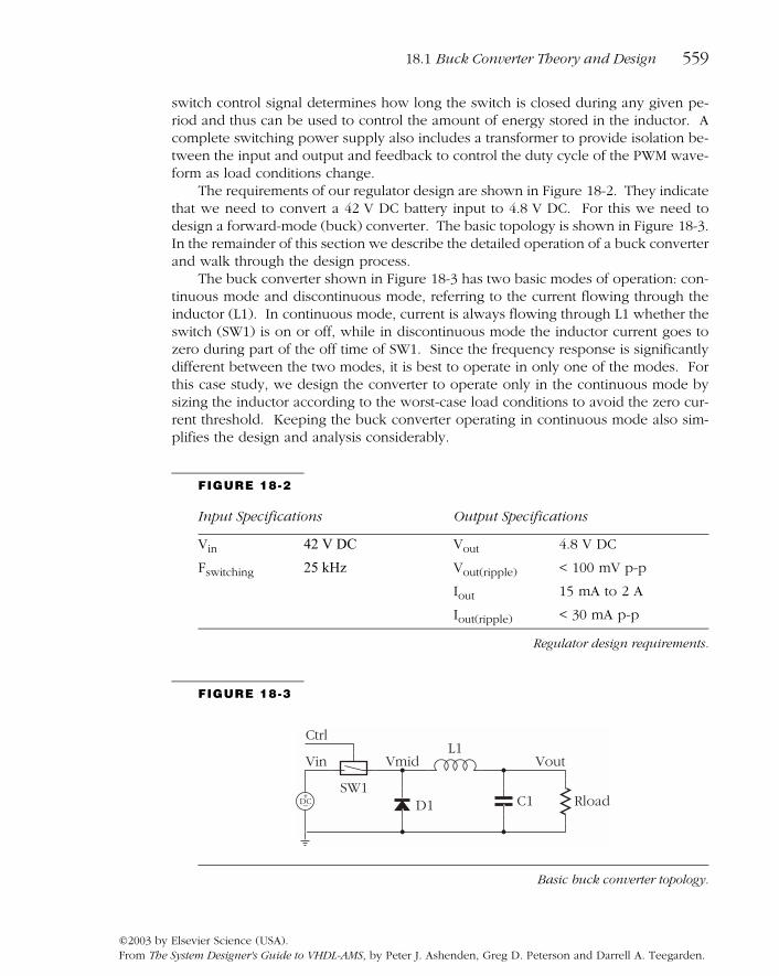
the device as a switch, it will be either on (saturated) or off, so its detailed character-istics are not relevant. We can proceed with simulations of the system using an ide-alized model of the device.
The switch model shown in Figure 18-10 models the on and off resistance andhas a linear transition between the two states. The switch is controlled by the portsw_state, which, in the power-supply system, is connected to the signal ctrl and drivenby the 25 kHz clock. This switch model provides sufficient detail for the early designstages, where we are designing the L-C filter and performing load analysis. For moredetailed analysis, we could substitute an architecture that provides logarithmic transi-tions between on and off resistances, or use a SPICE-based model, as described inAppendix A.
FIGURE 18-10
library ieee; use ieee.std_logic_1164.all;library ieee_proposed; use ieee_proposed.electrical_systems.all;
entity switch_dig isgeneric ( r_open : resistance := 1.0e6;
r_closed : resistance := 1.0e–3;trans_time : real := 1.0e–9 );
port ( sw_state : in std_logic;terminal p1, p2 : electrical );
end entity switch_dig;
––––––––––––––––––––––––––––––––––––––––––––––––––––
architecture linear of switch_dig is
signal r_sig : resistance := r_open;quantity v across i through p1 to p2;quantity r : resistance;
begin
–– detect switch state and assign resistance value to r_sigDetectState: process (sw_state)begin
if (sw_state'event and sw_state = '0') thenr_sig <= r_open;
elsif (sw_state'event and sw_state = '1') thenr_sig <= r_closed;
end if;end process DetectState;
r == r_sig'ramp(trans_time, trans_time);v == r * i;
end architecture linear;
Digitally controlled ideal switch model.

568 chapter eighteen Case Study 3: DC-DC Power Converter
©2003 by Elsevier Science (USA).From The System Designer's Guide to VHDL-AMS, by Peter J. Ashenden, Greg D. Peterson and Darrell A. Teegarden.
18.3 Voltage-Mode Control
As we saw in Section 18.1, the output voltage of the buck regulator is a function ofthe input voltage and the duty cycle of the switching waveform. Thus, we can adjustthe output voltage simply by changing the duty cycle. Pulse-width modulation (PWM)control techniques provide an effective way of doing this. The simplest method forcontrolling the output voltage level in PWM switching regulators is voltage-mode con-trol. This method involves sensing the output voltage in a closed-loop configuration,comparing to a reference voltage and adjusting the duty cycle of the PWM waveformbased on the error signal. In order to do this we need to modify the basic buck con-verter from Figure 18-3 to provide a voltage control input.
The schematic in Figure 18-11 shows one way to control the duty cycle of thePWM waveform. The control voltage is compared to a sawtooth waveform using acomparator with a digital output. The comparator output is then inverted, and theresulting waveform is used to control the switch.
Examining the simulation results in Figure 18-12, we see that a control voltage of0.327 V provides a PWM waveform, sw_ctrl, with the desired duty cycle of 13.1% cal-culated in Equation 18-6. This control voltage value was derived from the followingrelationship:
(18-15)
where Vc is the control voltage, and Vramp is the amplitude of the sawtooth waveform.Note that this equation is identical to Equation 18-5 with the duty cycle replaced bythe ratio Vc/Vramp. Setting Vramp to 2.5 V and solving for Vc, the equation becomes
FIGURE 18-11
Buck converter with voltage-mode PWM control.
+–
+–
+–DC
+–DC
comp_out
Vsaw
Vin
Vctrl
D1 C1 Rload
L1Vmid Vout
Vsaw
Vctrl 0.327 V
Vin 42 V
Comparator (digital output)
Sawtooth Generator
sw_ctrl
Vout Vin
Vc
Vramp
--------------× Vd–=

18.4 Averaged Model 569
©2003 by Elsevier Science (USA).From The System Designer's Guide to VHDL-AMS, by Peter J. Ashenden, Greg D. Peterson and Darrell A. Teegarden.
(18-16)
Note the resulting digital control signal is the same as that used in the originaldesign, with a duty cycle of 13.1%. In order to simulate this design, we need a fewadditional elementary models: a pulse waveform generator, an analog comparatorwith digital output (see Exercise 23) and a simple logic inverter. The simulation re-sults for the buck converter using this PWM control scheme are identical to thoseshown in Figure 18-8.
18.4 Averaged Model
We can replace the switching elements in the switched power supply with a state-averaged model, producing a smooth (averaged) voltage on the output. By replacingthe simulation-intensive switching model, the simulation times are significantly re-duced. An averaged model also allows us to run a small-signal frequency (AC) anal-ysis and examine the stability of the control loop. Furthermore, it allows us to run aclosed-loop time domain analysis and examine how the system responds to suddenchanges in load or line conditions. For our buck converter example, we can createan averaged model to replace the circuitry shown within the dashed box inFigure 18-11 (the diode, switch and digital control circuitry). The averaged model forthe buck converter operating in continuous mode contains the basic relationship fromEquation 18-15 and is shown in Figure 18-13. The simulation results using the aver-aged model and the switching model are compared in Figure 18-14. Note that theaveraged waveforms are a “smooth” approximation of the original waveforms.
FIGURE 18-12
Waveforms illustrating PWM voltage control technique.
-0.2
0.2
0.6
1.0
1.4
1.8
2.2
2.6
Vol
tage
(V
Vctrl
SW_CTRL
COMP_OUT
Vsawtooth)
1
01
0
14.65 14.67 14.68 14.69 14.70 14.71 14.72Time (ms)
C1: 14.651
C2: 14.657 (dx = 0.005) C3: 14.691 (dx = 0.040)
Vc Vramp
Vout Vd+
Vin
-----------------------× 2.54.8 0.7+
42---------------------× 0.327 V= = =

570 chapter eighteen Case Study 3: DC-DC Power Converter
©2003 by Elsevier Science (USA).From The System Designer's Guide to VHDL-AMS, by Peter J. Ashenden, Greg D. Peterson and Darrell A. Teegarden.
FIGURE 18-13
library ieee_proposed; use ieee_proposed.electrical_systems.all;
entity buck_sw isgeneric ( Vd : voltage := 0.7; –– diode voltage
Vramp : voltage := 2.5 ); –– p–p amplitude of ramp voltageport ( terminal input, output, ref, ctrl: electrical );
end entity buck_sw;
––––––––––––––––––––––––––––––––––––––––––––––––––––
architecture average of buck_sw is
quantity Vout across Iout through output to ref;quantity Vin across input to ref;quantity Vctrl across ctrl to ref;
begin
Vout == Vctrl * Vin / Vramp – Vd; –– averaged equation
end architecture average;
Averaged model for buck switching converter.
FIGURE 18-14
Simulation results for switching and averaged models.
4.71
4.73
4.75
4.77
4.79
4.81
Vol
tage
(V
Vout - switching
Vout - averaged
i ( L1 ) - switching
i ( L1 ) - averaged
)
1.9601.9651.9701.9751.9801.9851.9901.9952.000
Cur
rent
(A
)
4.791
1.9961
19.86 19.88 19.90 19.96 19.98 20.00Time (ms)
C1: 19.915

18.5 Closing the Loop 571
©2003 by Elsevier Science (USA).From The System Designer's Guide to VHDL-AMS, by Peter J. Ashenden, Greg D. Peterson and Darrell A. Teegarden.
18.5 Closing the Loop
At steady state, the output voltage of the power supply is only a function of the inputvoltage, diode voltage drop and duty cycle, as described earlier and shown inEquation 18-5. DC-DC converters, however are subject to sudden changes in condi-tions, such as input voltage (line) variations or output load changes. These changescan cause the output voltage to vary outside of the specified limits. To complete thedesign, we need to provide a feedback mechanism that senses a change in the outputvoltage and adjusts the duty cycle to bring the voltage back to the desired level.
The schematic for performing these types of analyses is shown in Figure 18-15.The hierarchical block buck_sw has replaced the switch, diode and PWM circuitry.This allows us to use either the switching model or the averaged model simply bychanging architectures, depending on the type of analysis required. Initially, we usethe averaged model shown in Figure 18-13; we will use the switching model later toexamine the effects of line and load transients. The load resistor has been replacedby a load model that can be enabled or disabled to provide sudden changes in theload conditions. The two-pole switch between the compensator and the control inputallows to use the same circuit for both open-loop and closed-loop simulations. Theposition of this switch is controlled by a generic parameter that we set prior to runninga simulation. Opening the switch breaks the loop so that the control-to-output trans-fer characteristic can be obtained. This information is useful for designing the com-pensation. The compensator block compares the output voltage to a reference andgenerates the appropriate control voltage. The block is introduced in the closed-loopconfiguration to allow stability analysis. We will discuss these models and the differ-ent types of analyses in more detail in the following sections.
FIGURE 18-15
Buck converter with voltage feedback.
+–DC
+–DC
C1 6 µF
L1 6.5 mH
ref
ref
output
p1
p2
p1
p2
Vmid
comp_2p2z
buck_sw
Voutinput
ctrl
sw2output
PWM
+–
(s + z1)(s + z2)
(s + p1)(s + p2)
LoadVin
42 V
Vctrl 0.327 V
Vref 4.8 V
Vctrl
inputVcomp_out
Vctrl_init

572 chapter eighteen Case Study 3: DC-DC Power Converter
©2003 by Elsevier Science (USA).From The System Designer's Guide to VHDL-AMS, by Peter J. Ashenden, Greg D. Peterson and Darrell A. Teegarden.
Compensation Design
The first step in designing the compensation is to determine the frequency character-istics of the system, commonly referred to as the “control-to-output” transfer charac-teristic or transfer function. To do this, we remove the load and break the feedbackloop, as discussed above. Figure 18-16 shows the model of the switch used to breakthe feedback loop. When the generic constant sw_state is 1, the common terminal cis connected to the terminal p1 with resistance r_closed and to p2 with resistancer_open. When sw_state is 2, the connections are reversed.
To generate the control-to-output transfer curve, we set sw_state to 2. This breaksthe loop and connects a voltage source of 0.327 V to the control input. For this anal-ysis, we must also remove the load. While we could do so simply by deleting theload, a more flexible approach is to add an “enable” generic constant. We will returnto this approach shortly. To generate the control-to-output transfer function, we need
FIGURE 18-16
library ieee_proposed; use ieee_proposed.electrical_systems.all;
entity sw_LoopCtrl isgeneric ( r_open : resistance := 1.0e6;
r_closed : resistance := 1.0e–3;sw_state : integer range 1 to 2 := 1 );
port ( terminal c, p1, p2 : electrical );end entity sw_LoopCtrl;
––––––––––––––––––––––––––––––––––––––––––––––––––––
architecture ideal of sw_LoopCtrl is
quantity v1 across i1 through c to p1;quantity v2 across i2 through c to p2;quantity r1, r2 : resistance;
begin
sw1 : if sw_state = 1 generater1 == r_closed;r2 == r_open;
end generate sw1;
sw2 : if sw_state = 2 generater1 == r_open;r2 == r_closed;
end generate sw2;
v1 == r1 * i1;v2 == r2 * i2;
end architecture ideal;
Switch model used to break the feedback loop.

18.5 Closing the Loop 573
©2003 by Elsevier Science (USA).From The System Designer's Guide to VHDL-AMS, by Peter J. Ashenden, Greg D. Peterson and Darrell A. Teegarden.
to perform a frequency analysis, as we discussed in Chapter 13. We sweep the fre-quency over a range of interest and use the resulting Bode plot to analyze the mag-nitude and phase response. The Bode plot of our control-to-output curve using theaveraged model is shown in Figure 18-17.
We can use the corner frequencies of the control-to-output curve to determine theplacement of the poles and zeros of the compensator design. The curve shows thedouble pole contributed by the L-C output filter at a frequency of 806 Hz, along witha –40 dB/decade rolloff and a –180° phase shift. This frequency can also be calculatedby
(18-17)
Note that we have substituted a capacitance value of 6 µF for the minimum value of1.5 µF in order to shift this pole slightly to the left, simplifying the compensator de-sign. The larger capacitor slows the time response, but also decrease the amount ofvoltage ripple on the output.
The Bode plot also reveals a zero occurring at about 530 kHz. This is due to the50 mΩ equivalent series resistance of the capacitor and can be calculated by
(18-18)
FIGURE 18-17
Control-to-output transfer characteristics.
Y1
-120.0
-100.0
-80.0
-60.0
-40.0
-20.0
0.0
20.0
40.0
60.0
Mag
nitu
de(d
B)
Y2
-200.0
-180.0
-160.0
-140.0
-120.0
-100.0
-80.0
-60.0
-40.0
-20.0
0.0
20.0
40.0
60.0
80.0
Pha
se(d
egre
es)
-47.07
56.63
-7.09
Y1VDB(VOUT)
Y2VP(VOUT)
e+2 1.0e+343
1.0e+443
1.0e+543
1.0e+643
1.0e+743
Frequency (Hz)
C2: 5.00e+4 (dx = 4.50e+4)C3: 8.06e+2 (dx = -4.19e+3)
C1: 5.00e+31.0e
fLC1
2π LC------------------ 1
2π 6.5 mH 6 µF×----------------------------------------------- 805.9 Hz= = =
fESR1
2πRESRC---------------------- 1
2π 50 mΩ 6 µF××------------------------------------------------ 530.5 kHz= = =
574 chapter eighteen Case Study 3: DC-DC Power Converter
©2003 by Elsevier Science (USA).From The System Designer's Guide to VHDL-AMS, by Peter J. Ashenden, Greg D. Peterson and Darrell A. Teegarden.
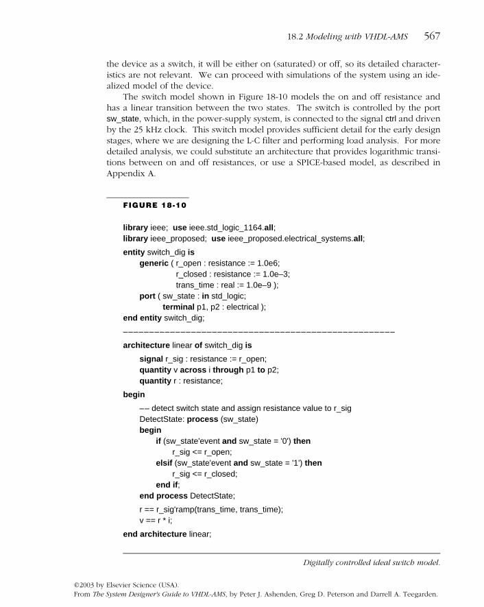
The detailed compensator design is beyond the scope of this book (see [7] and[40]), but generally the compensation should be designed to counteract the poles andzeros in the control-to-output response that may lead to instability. We choose a two-pole, two-zero method here due to the –40 dB/decade rolloff above the L-C poles andthe –180° phase lag. Factors to take into account when designing the compensationare the overall desired crossover frequency of the system, fxo, usually selected to bewell below the switching frequency (we select fxo = fs/5 = 5 kHz); the gain needed tobring the control-to-output transfer function up to 0 dB at the crossover frequency;and the pole and zero locations. We can see from Figure 18-17 that the required gainis 7.09 dB at 5 kHz. The zeros are typically placed at fLC/2 to counteract the L-C filterpoles, giving a resulting phase margin of 45°. One pole is placed well beyond thedesired crossover frequency (fp1 = 1.5fxo = 7.5 kHz) to increase the overall band-width. The second pole is placed at 531 kHz to compensate for the equivalent seriesresistance of the filter capacitor.
We can create a behavioral transfer function model containing the desired poleand zero locations and use it in the system simulation until the detailed compensatordesign is completed. The transfer function we use for the compensation is
(18-19)
where z1 and z2 are the zero locations and p1 and p2 are the pole locations. We canuse the 'ltf attribute to create high-level transfer function models. First the equationmust be simplified to the general form
(18-20)
Simplifying Equation 18-19 to this form gives us the following:
(18-21)
H s( )Vout
Vin
---------- K
sz1
----- 1+ s
z2
----- 1+
s sp1
----- 1+ s
p2
----- 1+ ×
-------------------------------------------------×= =
H s( )
aksk
k 0=
m
∑
bksk
k 0=
n
∑
--------------------a0 a1s a2s2 … amsm+ + + +
b0 b1s b2s2 … bnsn+ + + +---------------------------------------------------------------------= =
Vout
Vin
---------- K
s2
z1z2
----------- sz1 z2+
z1z2
----------------- 1+ +
s3
p1p2
----------- s2p1 p2+
p1p2
----------------- s+ +
-----------------------------------------------------×=

18.5 Closing the Loop 575
©2003 by Elsevier Science (USA).From The System Designer's Guide to VHDL-AMS, by Peter J. Ashenden, Greg D. Peterson and Darrell A. Teegarden.
Figure 18-18 shows a model that implements Equation 18-21. A high-level modelsuch as this simulates very quickly and is extremely useful when performing systemdesign trade-offs. Using this model, we can also easily modify the compensator polesand zeros to accommodate any unexpected system design changes that may occur.
The frequency analysis results for the compensator block (vcomp) overlaid on topof the original control-to-output transfer curve (vout) are shown in Figure 18-19.Again, since we are using very high-level models, we can easily adjust the desired re-sponse to accommodate design changes. For example, we could deemphasize thehigh Q of the L-C filter pole pair by separating the zeros. For now, this response issufficient to continue with our design until further information becomes available.
FIGURE 18-18
library ieee; use ieee.math_real.all;library ieee_proposed; use ieee_proposed.electrical_systems.all;
entity comp_2p2z isgeneric ( gain : real := 100.0; –– high DC gain for good load regulation
fp1 : real := 7.5e3; –– pole location to achieve crossover frequencyfp2 : real := 531.0e3; –– pole location to cancel effect of ESR fz1 : real := 403.0; –– zero locations to cancel L–C filter polesfz2 : real := 403.0 );
port ( terminal input, output, ref : electrical );end entity comp_2p2z;
––––––––––––––––––––––––––––––––––––––––––––––––––––
architecture ltf of comp_2p2z is
quantity vin across input to ref;quantity vout across iout through output to ref;constant wp1 : real := math_2_pi * fp1; –– Pole freq (in radians)constant wp2 : real := math_2_pi * fp2;constant wz1 : real := math_2_pi * fz1; –– Zero freq (in radians)constant wz2 : real := math_2_pi * fz2;constant num : real_vector := ( 1.0,
(wz1 + wz2) / (wz1 * wz2),1.0 / (wz1 * wz2) );
constant den : real_vector := ( 1.0e–9, 1.0,(wp1 + wp2) / (wp1 * wp2),1.0 / (wp1 * wp2) );
begin
vout == –1.0 * gain * vin'ltf(num, den);
end architecture ltf;
Behavioral model of the loop compensator.

576 chapter eighteen Case Study 3: DC-DC Power Converter
©2003 by Elsevier Science (USA).From The System Designer's Guide to VHDL-AMS, by Peter J. Ashenden, Greg D. Peterson and Darrell A. Teegarden.
FIGURE 18-19
Control-to-output transfer curve and compensator response.
Load Regulation
The next step is to place the compensator into the design shown in Figure 18-15 andrun the closed-loop time domain simulation. Before doing this, we need to changethe sw_state parameter on sw2 to 1 to close the loop and connect the output of thecompensator to the control input. We also reintroduce the load into the system. Toexamine how the system responds to a sudden change in load conditions, the originalresistor load model is replaced with a load model that changes value at a nominatedtime. The load model is shown in Figure 18-20. The load is basically a piecewise-linear resistor model with initial resistance res_init. At time t1 the resistance changesto res1, and at time t2 the resistance changes again to res2. This allows us to run atime domain simulation and examine the effect of instantaneous load changes on ourbuck converter. The model also has a generic parameter, load_enable, that is used toinsert or remove the load depending on the desired analysis.
The simulation results shown in Figure 18-21 arise from an initial resistance of2.4 Ω changing to 1 Ω at 5 ms, and to 5 Ω at 30 ms. The response shows that theloop is able to recover from the instantaneous change in load conditions, returningthe output to the desired 4.8 V.
-140.0-120.0
-100.0
-80.0-60.0
-40.0
-20.0
0.020.0
40.0
60.080.0
Mag
nitu
de(d
B)
-3.5
-2.5
-1.5
-0.5
0.5
1.5
2.5
3.5
4.5
Pha
se(r
adia
ns)
e+0 1.0e+1 1.0e+2 1.0e+3 1.0e+4 1.0e+5 1.0e+6 1.0e+7 1.0e+8
Frequency (Hz)1.0e
dB(vcomp)
dB(vout)
Phase(vcomp)
Phase(vout)

18.5 Closing the Loop 577
©2003 by Elsevier Science (USA).From The System Designer's Guide to VHDL-AMS, by Peter J. Ashenden, Greg D. Peterson and Darrell A. Teegarden.
FIGURE 18-20
library ieee_proposed; use ieee_proposed.electrical_systems.all;
entity pwl_load isgeneric ( load_enable : boolean := true;
res_init : resistance;res1 : resistance; t1 : time;res2 : resistance;t2 : time );
port ( terminal p1, p2 : electrical );end entity pwl_load;
––––––––––––––––––––––––––––––––––––––––––––––––––––
architecture ideal of pwl_load is
quantity v across i through p1 to p2;signal res_signal : resistance := res_init;
begin
load_present : if load_enable generate
if domain = quiescent_domain or domain = frequency_domain usev == i * res_init;
else v == i * res_signal'ramp(1.0e–6, 1.0e–6);
end use;
create_event : process isbegin
wait for t1;res_signal <= res1;wait for t2 – t1;res_signal <= res2;wait;
end process create_event;
end generate load_present;
load_absent : if not load_enable generate
i == 0.0;
end generate load_absent;
end architecture ideal;
Piecewise-linear load model.

578 chapter eighteen Case Study 3: DC-DC Power Converter
©2003 by Elsevier Science (USA).From The System Designer's Guide to VHDL-AMS, by Peter J. Ashenden, Greg D. Peterson and Darrell A. Teegarden.
FIGURE 18-21
Closed-loop time domain simulation results with changing load conditions.
Line Regulation
We can perform a similar test to examine how the supply responds to a change ininput (line) voltage. In the RC airplane system, the 42 V input voltage to the buckconverter is also used to power the propeller motor. If there is a sudden change inthis voltage, for example, due to a motor stall condition, the converter must be ableto continue regulating at 4.8 V. Figure 18-22 shows how the system responds to asudden droop in the input voltage from 42 V to 30 V. The transient response showsa corresponding droop in the output voltage of about 0.5 V and a recovery time ofabout 20 ms. These are important system-level performance measurements and willbe useful information when integrating the power converter with the rest of the RCairplane system.
18.6 Design Trade-Off Study
Now that we have completed and verified the basic design, we can use VHDL-AMSmodels and simulation as tools for studying the various design trade-offs. For exam-ple, we could study various topology decisions, such as selecting between differentconverter modes (buck mode versus forward mode), control methods (voltage modeversus current mode) and compensator topologies. We will not go into such a de-tailed level of design in this case study. Instead, we will consider one particular sys-tem design trade-off decision that can be made using high-level models and that can
-2.0
0.0
2.0
4.0
6.0
8.0
10.0
12.0
14.0
16.0
18.0
20.0
22.0V
olta
ge(V
)
4.80 4.78
VOUT
0 5.0 10.0 15.0 20.0 25.0 30.0m 35.0 40.0
Time (ms)C1: 2.87 (dx = -24.26)
C2: 27.130.0

18.6 Design Trade-Off Study 579
©2003 by Elsevier Science (USA).From The System Designer's Guide to VHDL-AMS, by Peter J. Ashenden, Greg D. Peterson and Darrell A. Teegarden.
assist in completing the detailed converter design. We will consider the trade-off be-tween the switching frequency and the values for the L-C filter.
As we saw in Equations 18-10 and 18-11, there is an inverse relationship betweenthe L-C values and the clock frequency. Other factors affect these values as well(namely, output voltage and current), but the selection of the clock speed is a con-trollable design parameter and is somewhat arbitrary. The system design challenge isto find the optimum L-C values and clock speed that meet the overall system require-ments. We can use the equations mentioned above to manually calculate differentvalues for Lmin and Cmin for given clock frequencies. Alternatively, we can expressthe equations in a VHDL-AMS model and use a simulator to calculate the values. Anexample of such a model is shown in Figure 18-23. This model contains all the basicrelationships from Equations 18-1 through 18-11. The input parameters (Vout, Vin, Im-in, Vripple, Vd) are generic constants with default values taken from the system speci-fication. The switching frequency is input using a quantity port so that it can be easilyvaried during a simulation by a ramped source model. The outputs Lmin and Cminare output quantity ports that can be plotted.
FIGURE 18-23
library ieee_proposed; use ieee_proposed.electrical_systems.all;
entity CalcBuckParams is
generic ( Vin : voltage range 1.0 to 50.0 := 42.0; –– input voltage [volts]Vout : voltage := 4.8; –– output voltage [volts]Vd : voltage := 0.7; –– diode voltage [volts]Imin : current := 15.0e–3; –– min output current [amps]
(continued on page 580)
FIGURE 18-22
Simulation results of converter output with sudden change in input voltage.
4.254.304.354.404.454.504.554.604.654.704.754.804.854.904.95
Vol
tage
(V)
4.80044.8000
VOUT
0 5.0m 10.0m 15.0 20.0 25.0 30.0 35.0 40.0
Time (ms)C2: 36.54 (dx = 31.25)
C1: 5.290.0

580 chapter eighteen Case Study 3: DC-DC Power Converter
©2003 by Elsevier Science (USA).From The System Designer's Guide to VHDL-AMS, by Peter J. Ashenden, Greg D. Peterson and Darrell A. Teegarden.
(continued from page 579)
Vripple : voltage range 1.0e–6 to 100.0:= 100.0e–3 ); –– output voltage ripple [volts]
port ( quantity Fsw : in real range 1.0 to 1.0e6:= 2.0; –– switching frequency [Hz]
quantity Lmin : out inductance; –– minimum inductance [henries]quantity Cmin : out capacitance ); –– minimum capacitance [farads]
end entity CalcBuckParams;
––––––––––––––––––––––––––––––––––––––––––––––––––––
architecture behavioral of CalcBuckParams is
constant D : real := (Vout + Vd) / Vin; –– duty cyclequantity Ts : real; –– periodquantity Ton : real; –– on time
begin
Ts == 1.0 / Fsw;
Ton == D * Ts;
Lmin == (Vin – Vout) * Ton / (2.0 * Imin);
Cmin == (2.0 * Imin) / (8.0 * Fsw * Vripple);
end architecture behavioral;
Model for calculating L and C values for the buck converter.
For the simulation, we use a pulse source with a quantity port output to sweepthe input frequency from 25 kHz to 200 kHz. The simulation results are shown inFigure 18-24. Inductance values for switching frequencies of 50 kHz and 100 kHz arehighlighted. The results verify the inverse relationship between Lmin and the clock-switching frequency mentioned above and allow us to quickly find the appropriatevalues for each.
The model could be expanded further to include the poles and zeros for the be-havioral compensator model in Figure 18-18 (see Exercise 18). Such a model can bevery useful, since many of the circuit parameters are interrelated. For example, chang-ing the switching frequency changes the values for L and C, which also changes thecontrol-to-output transfer curve (see Figure 18-17) by moving the location of the dou-ble pole. This changes the compensation requirements and probably affects systemperformance. Using high-level models, such as the state-averaged model of the switchand the transfer function model for the compensator, we can run system-level simu-lations very quickly to optimize system performance prior to completing the detaileddesign.
To illustrate this, we repeated the line regulation test from Figure 18-22, simulta-neously varying the L and C values and the pole and zero locations of the compensa-tor according to the values calculated by the model in Figure 18-23. The results areshown in Figure 18-25. Examining this plot closely reveals an inverse relationship be-tween the output voltage droop and settling time as a function of switching frequency.

18.6 Design Trade-Off Study 581
©2003 by Elsevier Science (USA).From The System Designer's Guide to VHDL-AMS, by Peter J. Ashenden, Greg D. Peterson and Darrell A. Teegarden.
The relationships can be plotted, as shown in Figure 18-26, by performing a series ofmeasurements on the original simulation data. The plot reveals that, as the switchingfrequency is increased, a definite trade-off exists between maximum voltage droopand the settling time when the system is recovering from a sudden change in the linevoltage.
FIGURE 18-24
Inductance versus switching frequency.
FIGURE 18-25
Line regulation for various switching frequencies.
0.5
1.0
1.5
2.0
2.5
3.0
3.5
4.0
4.5
5.0
5.5
6.0
6.5
7.0
Indu
ctan
ce(m
H)
1.62
3.25
40.0 60.0k 80.0 100.0 120.0 140.0 160.0 180.0 200.0
Freq (kHz)C2: 100.00 (dx = 50.00)
C1: 50.00
Lmin
3.73.83.94.04.14.24.34.44.54.64.74.84.95.0
Vol
tage
(V)
0m 2.0 4.0 6.0 8.0 12.0 16.0 20.0 24.0 28.0
Time (ms)0.0
VOUT (Fs = 25 kHz)VOUT (Fs = 30 kHz)VOUT (Fs = 40 kHz)VOUT (Fs = 50 kHz)VOUT (Fs = 75 kHz)VOUT (Fs = 100 kHz)VOUT (Fs = 125 kHz)VOUT (Fs = 150 kHz)
VOUT (Fs = 200 kHz)

582 chapter eighteen Case Study 3: DC-DC Power Converter
©2003 by Elsevier Science (USA).From The System Designer's Guide to VHDL-AMS, by Peter J. Ashenden, Greg D. Peterson and Darrell A. Teegarden.
FIGURE 18-26
Output voltage droop and settle time measurements.
Exercises
1. [➊ 18.1] For a buck converter, what is the relationship between input voltage, out-put voltage and duty cycle?
2. [➊ 18.1] What topology is be needed to convert 4.8 VDC to 42 VDC?
3. [➊ 18.1] What is the main purpose of adding a transformer to complete the DC-DC converter design?
4. [➊ 18.1] How is the operation of the buck converter affected if the load resistancerises above the maximum allowed value?
5. [➊ 18.2] Why is the ideal switch model sufficient for much of the buck converterdesign process?
6. [➊ 18.4] What is the advantage of the averaged model over the switching modelwhen designing a buck converter?
7. [➊ 18.5] What role does the compensation block play in the buck converter de-sign, and why is it advantageous to use a behavioral model that utilizes the 'ltfattribute?
8. [➊ 18.5] What is the purpose of the two-pole switch (SW2) in Figure 18-15?
9. [➊ 18.5] How do you generate the control-to-output transfer curve, and what is itused for?
Y1
0.50
0.55
0.60
0.65
0.70
0.75
0.80
0.85
0.90
0.95
1.00
1.05V
olta
ge(V
)Y2
2.0
4.0
6.0
8.0
10.0
12.0
14.0
16.0
18.0
20.0
Tim
e(m
s)
Y1
Y2
40.0 60.0 80.0 100.0 120.0 140.0 160.0 180.0 200.0
Frequency (kHz)
VOLTAGE_DROOP
SETTLE_TIME

Exercises 583
©2003 by Elsevier Science (USA).From The System Designer's Guide to VHDL-AMS, by Peter J. Ashenden, Greg D. Peterson and Darrell A. Teegarden.
10. [➊ 18.6] What is the relationship between the L-C values and switching frequency?
11. [➋ 18.2] Create a model for a linear resistor with electrical ports that includes therelationship .
12. [➋ 18.2] Add an architecture to the resistor model where the resistance varies lin-early with temperature. Hint: Use the equation
where Rnom is the nominal resistance, α is the linear temperature coefficient andTenv is the ambient temperature in °C.
13. [➋ 18.2] Create a model for a linear capacitor with electrical ports that includesthe relationship
14. [➋ 18.2] Create a model for a linear inductor with electrical ports that includes therelationship
15. [➋ 18.2] Create a model for a diode with electrical ports that includes the rela-tionship
16. [➋ 18.2] Create a model for a constant (DC) voltage source.
17. [➋ 18.6] Create a pulse source with a quantity port output to test the CalcBuck-Params model in Figure 18-23.
18. [➋ 18.6] Modify the model in Figure 18-23 to calculate the poles and zeros for thecompensator model.
19. [➌ 18.1] Write a test bench with a 25 kHz digital clock to run the structural VHDL-AMS model shown in Figure 18-7, and verify the simulation results.
20. [➌ 18.2] Add an architecture to the capacitor model that includes leakage resis-tance. Hint: Use a second through variable to define a parallel resistance acrossthe capacitor terminals.
v i R×=
RT Rnom 1 α Tenv 27°C–( )+( )=
i vtd
dv×=
i L v td∫×=
i isat ev vt⁄ 1–( )=
584 chapter eighteen Case Study 3: DC-DC Power Converter
©2003 by Elsevier Science (USA).From The System Designer's Guide to VHDL-AMS, by Peter J. Ashenden, Greg D. Peterson and Darrell A. Teegarden.
21. [➌ 18.2] Add an architecture to the switch model in Figure 18-10 to provide alogarithmic transition between the on and off resistances.
22. [➌ 18.2] Create a behavioral model for a two-winding transformer with the fol-lowing equations:
where the subscript p signifies the primary winding and the subscript s signifiesthe secondary winding.
23. [➌ 18.3] Write a model for a comparator with electrical input pins and a digital(std_logic) output pin for the PWM control method shown in Figure 18-11.
24. [➌ 18.5] Design a detailed (component-level) compensator circuit and comparethe simulation results to the behavioral models in Figure 18-18.
25. [➍ 18.4] Modify the averaged model in Figure 18-13 to handle discontinuousmode.
26. [➍ 18.5] Create a model for a complete forward converter that includes a trans-former, snubber circuitry and a detailed compensator design.
27. [➍ 18.5] Create a PWL load model where the (time, resistance) pairs are a two-dimensional array of variable length.
28. [➍ ] Create a battery model that has inputs of voltage and amp-hour ratings witha state-of-charge and voltage-versus-time outputs.
vp Ip Rp× Lp td
dIp× mtd
dIs×+ +=
vs Is Rs× Ls td
dIs× mtd
dIs×+ +=