Embed Size (px)
Citation preview

Instructions for use
Title Cathodic pulse breakdown of anodic films on aluminium in alkaline silicate electrolyte : Understanding the role ofcathodic half-cycle in AC plasma electrolytic oxidation
Author(s) Sah, Santosh Prasad; Tsuji, Etsushi; Aoki, Yoshitaka; Habazaki, Hiroki
Citation Corrosion Science, 55: 90-96
Issue Date 2012-02
Doc URL http://hdl.handle.net/2115/48644
Type article (author version)
File Information CS55_90-96.pdf
Hokkaido University Collection of Scholarly and Academic Papers : HUSCAP
1
Cathodic Pulse Breakdown of Anodic Films on Aluminium in Alkaline Silicate Electrolyte
– Understanding the Role of Cathodic Half-cycle in AC Plasma Electrolytic Oxidation
Santosh Prasad Sah, Etsushi Tsuji, Yoshitaka Aoki and Hiroki Habazaki*
Division of Materials Chemistry, Faculty of Engineering, Hokkaido University, Sapporo,
Hokkaido, 060-8628, Japan
*Corresponding author: Phone & Fax: +81-11-706-6575, e-mail: [email protected]
2
Abstract
Sequential anodic and cathodic pulse voltages were applied on anodized Al micro-electrodes in
alkaline silicate electrolyte to explore the role of cathodic pulse in AC or bipolar plasma
electrolytic oxidation (PEO) process. SEM observation was carried out to observe the sites of
anodic and cathodic breakdown and their morphologies. The prior anodic breakdown accelerated
the cathodic breakdown at -50 V, and the acceleration was associated with the preferential
cathodic breakdown at the anodic breakdown sites. However, the succeeding anodic breakdown
during applying anodic pulse of 420 V for 2 ms was highly suppressed at the cathodic breakdown
sites.
Keywords: A: aluminium, B: SEM, C: anodic films
1. Introduction
Plasma electrolytic oxidation (PEO), often also referred to as micro-arc oxidation, spark
anodizing or micro-plasma oxidation, has attracted recent attention as a surface engineering
process of light metals (Al, Mg and Ti) and their alloys to form ceramic coatings [1] . The
thickness of the coatings ranges from tens to hundreds of micrometers, and show good
thermo-mechanical properties, corrosion resistance and tribological properties [1-14]. The process
involves generation of a large number of short-lived microdischarges on the entire substrate
surface. The microdischarges, caused by dielectric breakdown of oxide coatings at high voltages,
induce rapid heating and cooling of the coatings, forming highly crystalline, often
3
high-temperature phases. The coatings contain many characteristic discharge channels, with the
channels becoming larger with the time of PEO treatment, such that the coatings formed by PEO
are essentially porous. Thus, large discharge pores (with diameter larger than 10 µm) connecting
the inner coating close to the metal/film interface with the oxide surface, are often found in the
PEO coatings. Such large discharges are detrimental for corrosion and wear resistance of the
coatings. Destructive discharges are found to be avoided by employing AC or bipolar power
supply and proper electrolytes.
Recently, much attention is paid to ‘soft’ sparking of PEO, which is often observed at a
selected AC or bipolar PEO condition with higher cathodic current with respect to the anodic
current [15-20]. Under the ‘soft’ sparking condition, the formation of a relatively dense and
uniform coating of ~100 μm thickness is promoted. The ‘soft’ sparking is characterized by
reduction in the rms voltage and greatly reduced acoustic emission and increased emissions from
bound-free electron transitions in the optical emission spectrum [15, 16 ]. Three-layer coatings are
usually formed under the ‘soft’ sparking condition, comprising an outer layer with a highly porous
morphology, a relatively thick and dense intermediate layer and an inner thin barrier layer [21].
The transition to the ‘soft’ sparking on aluminium is also accelerated by the presence of
pre-formed anodic porous alumina layer [18, 22]. The recent extensive studies of the PEO process
are improving the coating properties, but the key factors that control the PEO process are not yet
fully understood.
Since micro-discharges play a crucial role in the growth of PEO coatings, understanding of the
factors affecting characteristics of dielectric discharges and resultant morphology of discharge
channels is of importance. So far, the ‘soft’ sparking has been observed only in alkaline silicate
electrolyte, and recently, we have reported that electrolyte as well as pulse voltage during single
4
pulse anodizing influences largely the morphology of discharge channels. In alkaline silicate
electrolyte groove-like discharge channels are formed predominantly and healing of discharge
pores is promoted in this electrolyte [23].
The ‘soft’ sparking occurs under AC or bipolar PEO. Further, it is well accepted that dense
coatings with less micro-cracks are obtained by AC PEO compared with DC PEO [24]. However,
the role of cathodic process in PEO is not yet well understood. In the present study, cathodic
breakdown of the anodic oxide films has been examined by applying a single cathodic pulse
voltage on a pre-anodized aluminium micro-electrode. The influence of the cathodic breakdown in
the succeeding anodic breakdown is also examined for a better understanding the AC PEO process.
An aluminium microelectrode is used in this study to reduce the number of discharge events on the
entire surface and hence to assist more ready analysis of the breakdown behaviour.
2. Experimental
Highly pure aluminium wire (99.99%, Nilaco Corporation) of 0.2 mm diameter was first
anodized up to 450 V in 0.01 mol dm-3
ammonium pentaborate electrolyte to cover the entire wire
surface by a thick anodic oxide film. Then, the anodized wire was embedded in resin. The
embedded aluminium wire was sectioned by ultramicrotomy technique (RMC, MT-7) using a
glass knife to expose a clean and relatively flat surface (hereafter denoted as as-polished Al
specimen). The specimen was then anodized in alkaline silicate electrolyte of 0.075 mol dm-3
Na2SiO3 + 0.05 mol dm-3
KOH (pH 12.5) to 350 V at a sweep rate of 3.5 V s-1
and held at 350 V for
50 s (350 V-anodized Al specimen). Anodic pulse voltage of 420 V with pulse width of 2 ms and
cathodic pulse voltage of -50 V with a pulse width of either 10 ms or 1 s were applied solely or in
5
sequence. The application of the extended cathodic pulse width (1 s), unlike a practical value of 5
or 10 ms, was carried out to visualize the morphological change in anodic oxide film or metal
substrate clearly. The voltage waveforms were fed from a Hokuto-Denko, HB-105 function
generator to a Chroma, 61501 Programmable AC Source. Current transients were recorded with a
sampling time of 0.1 ms using an Agilent 3441A digital multimeter controlled by NI Labview
software. The oxide films of selected specimen were chemically stripped out in a mixed solution
of 20 g L-1
CrO3 and 45 ml L-1
H3PO4 at 363 K for 1.8 ks to expose the metal surface. The surface
of oxide film as well as metal substrate was observed with JEOL JSM-6500F field-emission
electron microscope (SEM).
3. Results
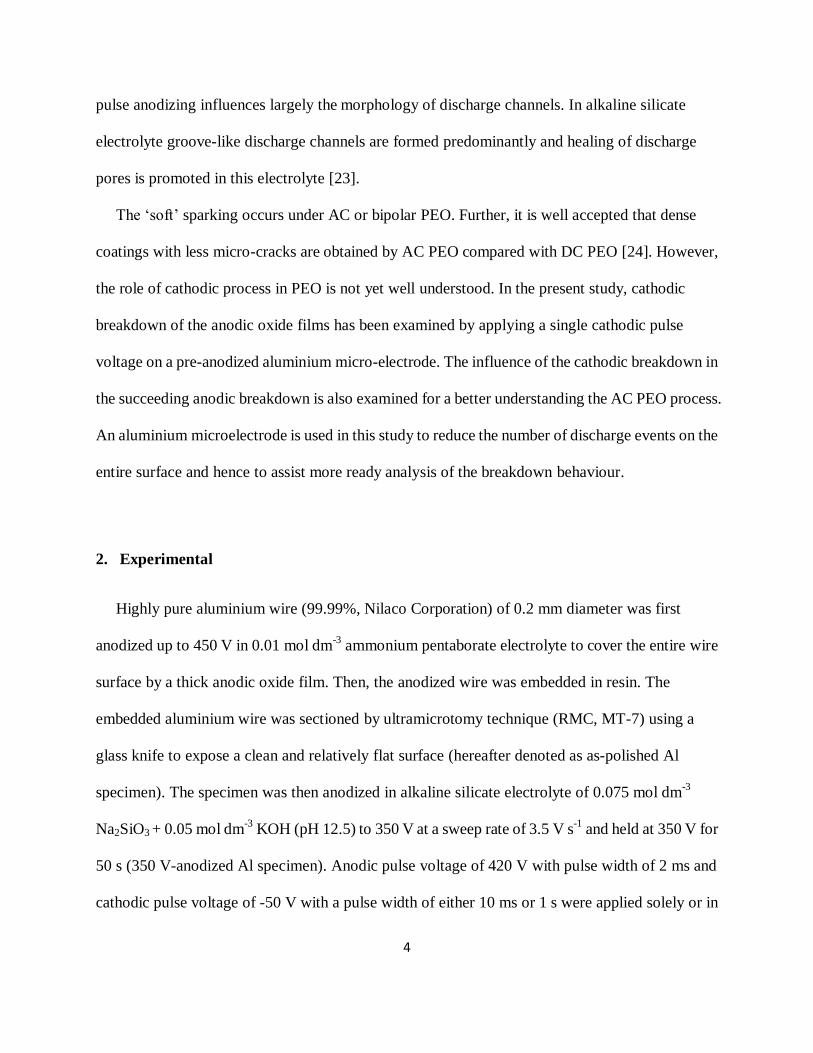
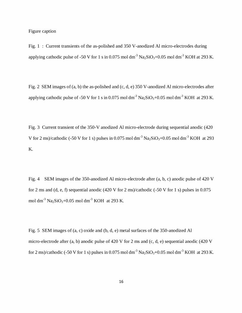
Fig. 1 shows the current transient during applying -50 V pulse voltage for 1 s on the as-polished
and 350 V-anodized Al specimens. For the as-polished specimen, the cathodic current increases
immediately to ~150 A cm-2
and oscillates largely between 2 and 190 A cm-2
. Such current
oscillations may be associated with the generation of hydrogen gas, which may cover the small
electrode surface repeatedly [25]. Such large current fluctuation is a characteristic of the
micro-electrode, since such large current fluctuation was not observed for the aluminium specimen
of ~1 cm2 size. When the cathodic pulse voltage is applied to the 350 V-anodized Al specimen, the
initial cathodic current is as low as 1 A cm-2
, and the cathodic current increase to the order of 10 A
cm-2
, which may be associated with film breakdown by hydrogen generation [20], occurs after
~120 ms. From the repeated experiments, the time to reach the breakdown for the 350 V-anodized
specimens varied between 15 and 250 ms. Therefore, the cathodic breakdown of 350 V-anodized
Al by applying -50 V pulse for 10 ms or less (a practical value of cathodic pulse time in actual
6
PEO) is not possible. The current after breakdown of the anodic film is still low, compared with
the as-polished specimen. The breakdown of the anodic film might occur locally, not on entire
surface, resulting in the relatively low cathodic current.
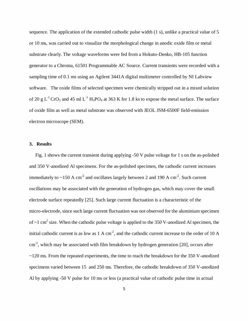
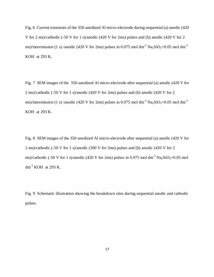
Figs. 2a and 2b show the SEM images of the as-polished specimen after application of -50
V for 1 s. In the low magnification image (Fig. 2a), the surface of aluminium micro-electrode,
which is surrounded by resin, is uniform and no remarkable features are visible. The high
magnification image (Fig. 2b) reveals that the aluminium surface is covered with a nanoporous
layer, which is probably composed of a hydrated alumina corrosion product. In contrast, the 350
V-anodized specimen shows locally damaged surface after application of the cathodic pulse (Fig.
2c). Obviously, the anodic film is broken locally and the development of a porous hydrated oxide
layer is visible at a breakdown site (Fig. 2d). In other regions, where no breakdown occurred,
anodic oxide film is remained with embryo of a porous layer developing due to alkaline nature of
the electrolyte used (Fig. 2e).
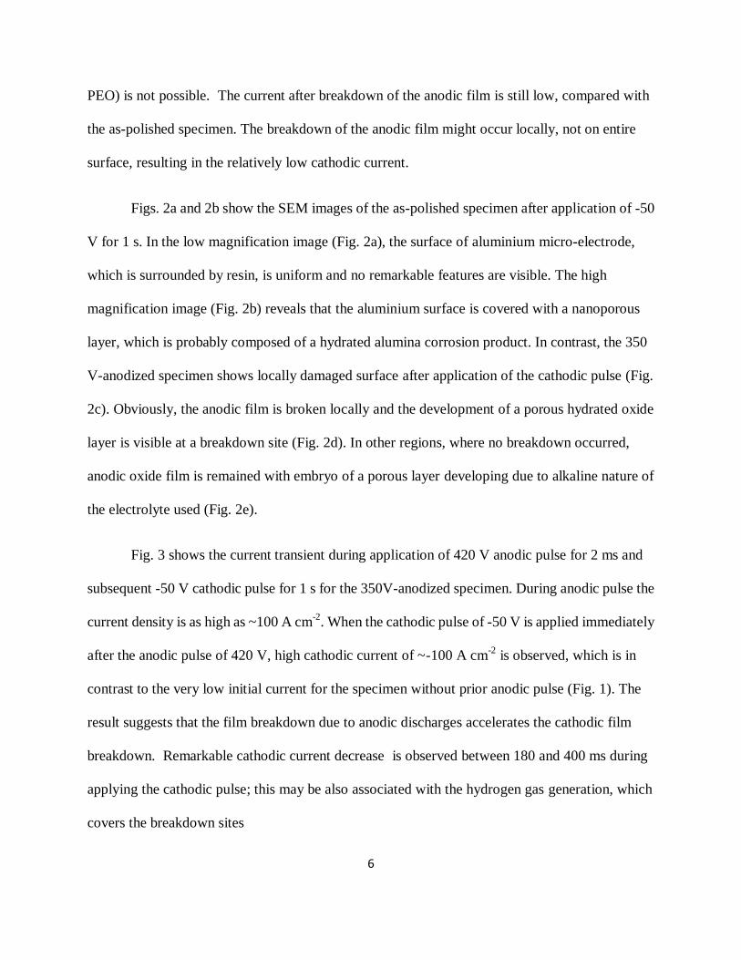
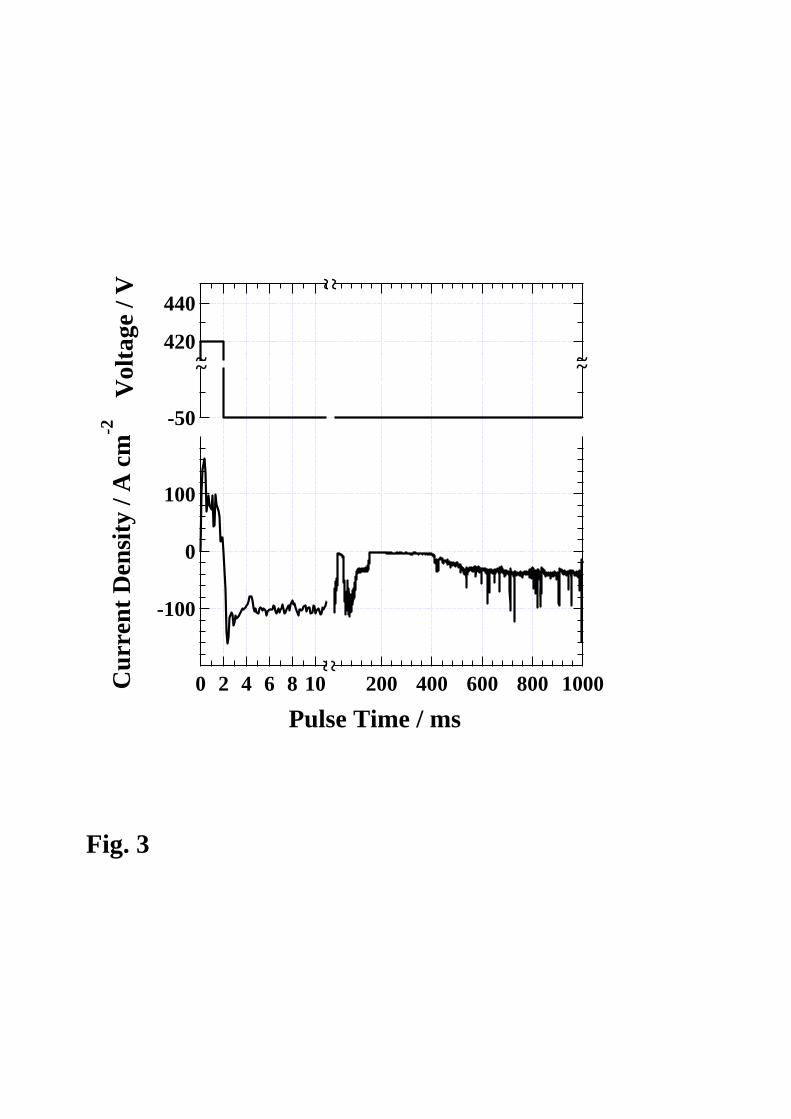
Fig. 3 shows the current transient during application of 420 V anodic pulse for 2 ms and
subsequent -50 V cathodic pulse for 1 s for the 350V-anodized specimen. During anodic pulse the
current density is as high as ~100 A cm-2
. When the cathodic pulse of -50 V is applied immediately
after the anodic pulse of 420 V, high cathodic current of ~-100 A cm-2
is observed, which is in
contrast to the very low initial current for the specimen without prior anodic pulse (Fig. 1). The
result suggests that the film breakdown due to anodic discharges accelerates the cathodic film
breakdown. Remarkable cathodic current decrease is observed between 180 and 400 ms during
applying the cathodic pulse; this may be also associated with the hydrogen gas generation, which
covers the breakdown sites
7
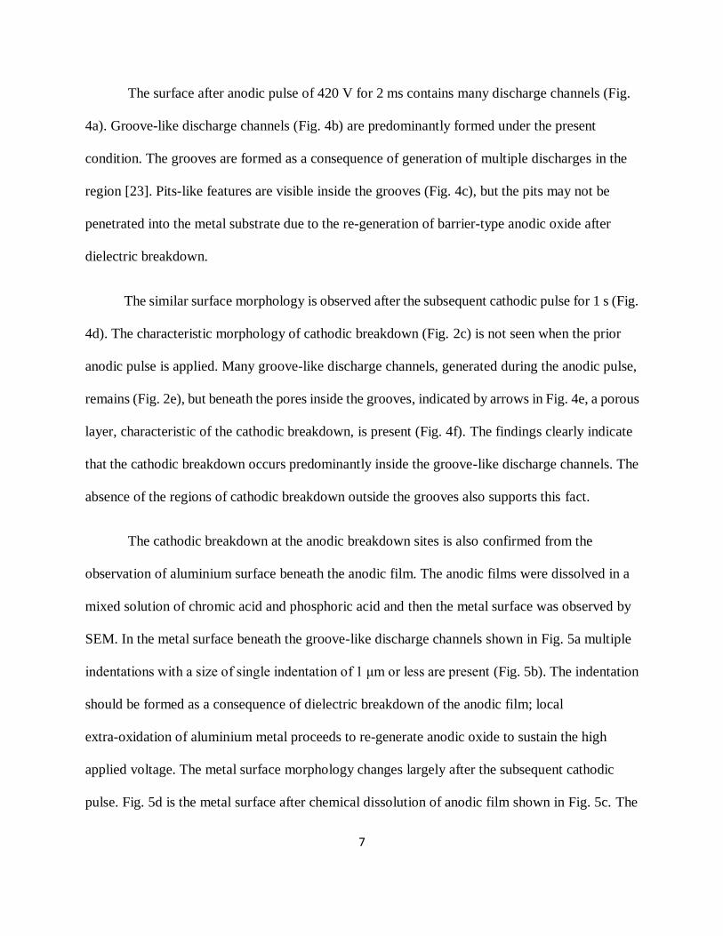
The surface after anodic pulse of 420 V for 2 ms contains many discharge channels (Fig.
4a). Groove-like discharge channels (Fig. 4b) are predominantly formed under the present
condition. The grooves are formed as a consequence of generation of multiple discharges in the
region [23]. Pits-like features are visible inside the grooves (Fig. 4c), but the pits may not be
penetrated into the metal substrate due to the re-generation of barrier-type anodic oxide after
dielectric breakdown.
The similar surface morphology is observed after the subsequent cathodic pulse for 1 s (Fig.
4d). The characteristic morphology of cathodic breakdown (Fig. 2c) is not seen when the prior
anodic pulse is applied. Many groove-like discharge channels, generated during the anodic pulse,
remains (Fig. 2e), but beneath the pores inside the grooves, indicated by arrows in Fig. 4e, a porous
layer, characteristic of the cathodic breakdown, is present (Fig. 4f). The findings clearly indicate
that the cathodic breakdown occurs predominantly inside the groove-like discharge channels. The
absence of the regions of cathodic breakdown outside the grooves also supports this fact.
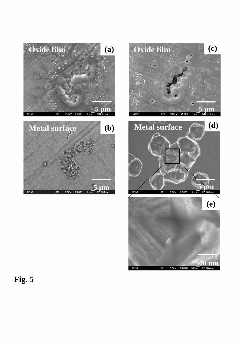
The cathodic breakdown at the anodic breakdown sites is also confirmed from the
observation of aluminium surface beneath the anodic film. The anodic films were dissolved in a
mixed solution of chromic acid and phosphoric acid and then the metal surface was observed by
SEM. In the metal surface beneath the groove-like discharge channels shown in Fig. 5a multiple
indentations with a size of single indentation of 1 μm or less are present (Fig. 5b). The indentation
should be formed as a consequence of dielectric breakdown of the anodic film; local
extra-oxidation of aluminium metal proceeds to re-generate anodic oxide to sustain the high
applied voltage. The metal surface morphology changes largely after the subsequent cathodic
pulse. Fig. 5d is the metal surface after chemical dissolution of anodic film shown in Fig. 5c. The
8
cathodic pulse changes the multiple indentations developed during anodic pulse to large craters of
several micrometers in size. From the images shown in Figs. 5d and 5e it is likely that the craters
appear to develop due to faceted dissolution of aluminium during applying cathodic pulse for 1 s.
Next, the influence of the cathodic pulse on the anodic discharge during the succeeding
anodic pulse has been examined. Fig. 6a shows a current transient during the sequential anodic
pulse (420 V, 2 ms)/cathodic pulse (-50 V, 1 s)/anodic pulse (420 V, 2 ms). For comparison, the
current transient during two anodic pulses of 420 V for 2 ms with intermission for 1 s is revealed
(Fig. 6b). Comparable anodic currents are obtained for the 1st and 2
nd anodic pulses when no
cathodic voltage is applied. From the repeated experiments of more than four times, the electric
charge passed during the first anodic pulse is 139 ± 19 mC cm-2
while that during the second
anodic pulse is 171 ± 20 mC cm-2
. In contrast, when the cathodic pulse of 1 s is applied, the current
during the second anodic pulse is almost one order of magnitude lower than that during the first
anodic pulse (Fig. 6a). The electric charge is also reduced from 139 ± 19 mC cm-2
for the first
anodic pulse to 15 ± 5 mC cm-2
for the second anodic pulse. Therefore, the cathodic pulse affects
largely the succeeding anodic discharge. When the cathodic pulse time was reduced to 10 ms, the
current during the second anodic pulse increased, and the electric charge during the second anodic
pulse is approximately 0.58 ± 0.09 of that during the first anodic pulse. Thus, even for the short
cathodic pulse, the anodic discharges during the succeeding anodic pulse are suppressed to some
extent.
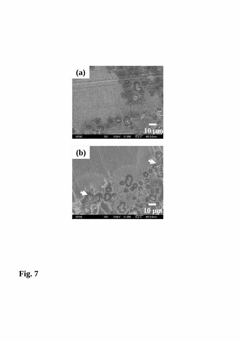
Surface observations after the second anodic pulse reveal that larger discharge channels of
~35 μm in size are developed, as indicated arrows in Fig. 7b, after the second anodic pulse with the
intermission for 1 s, while the size of the discharge channels of 15 μm or less is maintained even
9
after the second anodic pulse with cathodic pulse (Fig. 7a). During the second anodic pulse after
the intermission for 1 s, the dielectric breakdown appears to occur preferentially in the groove-like
discharge channels developed during the first anodic pulse, enlarging the discharge channels.
When the cathodic pulse is applied between two anodic pulses, no such large discharge channels
are absent. The discharge channels formed during the first anodic pulse appear to become more
resistive for the succeeding anodic breakdown after the cathodic breakdown, leading to the
remarkable reduction of the current during the second anodic pulse. When the second anodic pulse
of 300 V was applied after the cathodic pulse, a porous layer in the discharge channels (Fig. 8a and
8b) changed to an apparently non-porous layer. Since no anodic breakdown occurs at this anodic
voltage, this non-porous layer is developed by usual growth of anodic oxide without dielectric
breakdown. Even when the second anodic pulse of 420 V is applied, similar non-porous oxide
layer is found in the discharge channels (upper-right discharge channel of Fig. 8c and 8d). In
addition, new discharge channels are developed during the second anodic pulse, as indicated by an
arrow in Fig. 8c.
4. Discussion
The findings obtained in the present study should be of importance for understanding the
AC PEO of aluminium and its alloys. Relatively large discharge pores are usually developed in the
PEO coatings and the pore size increases with thickening of the coatings [27]. However, if the
‘soft’ sparking condition is established, relatively compact and thick intermediate layer develops,
although an outer layer is still rather rough and highly porous [21]. The ‘soft’ sparking has been
reported only in alkaline silicate electrolyte for aluminium and its alloys. Further, larger cathodic
10
current with respect to the anodic current in AC or bipolar PEO is one of the essential requisites for
‘soft’ sparking. Thus, the cathodic process should have a crucial role in establishing the ‘soft’
sparking condition in AC PEO.
The present study reveals that the cathodic breakdown is accelerated by the presence of
anodic discharge channels developed by dielectric breakdown of an anodic film at high anodic
pulse voltage. The acceleration is associated with the preferential cathodic breakdown at the
anodic breakdown sites, where groove-like discharge channels are mainly formed. This means that
the anodic film re-generated at the anodic breakdown sites during anodic pulse is less resistive for
cathodic breakdown than the regions where no breakdown occurs. This is true even for the second
anodic breakdown such that discharge channels of enlarged sizes are developed during the second
anodic pulse when no cathodic pulse applies between two anodic pulses. The formation of
less-protective film at the anodic breakdown sites must be electrolyte-dependent; in ammonium
pentaborate electrolyte, a more resistive film is re-generated at the anodic breakdown sites [23].
It has been reported that an anodic film is locally broken due to hydrogen gas generation
beneath the anodic film during cathodic polarization [28]. It is generally hypothesized that such
cathodic breakdown may introduce the sites for next anodic breakdown. However, an opposite
result is obtained in the present study. Although the anodic breakdown sites are less protective, the
sites change to be more protective after the cathodic breakdown, such that anodic dielectric
breakdown in the succeeding anodic pulse occurs preferentially in the regions where no prior
breakdown occurs. Improved protectiveness of the cathodic breakdown sites avoids the repeated
breakdown at the same sites, which induce the generation of large discharge pores. The cathodic
breakdown in the silicate electrolytes can thus randomize the anodic breakdown sites, probably
11
contributing to the formation of more uniform PEO coatings in this electrolyte. The suppression of
the anodic breakdown in the succeeding anodic pulse was remarkable when relatively long
cathodic pulse width was applied. Such breakdown behaviour in sequential anodic and cathodic
pulse voltages is schematically illustrated in Fig. 9. The present finding on the effective
suppression of anodic breakdown after the longer cathodic pulse may also be correlated to the
requisite of the higher cathodic current with respect to the anodic current for establishing the ‘soft’
sparking.
5. Conclusions
1. Cathodic breakdown of anodic film on aluminium in alkaline silicate electrolyte at -50 V
occurs preferentially at the prior anodic breakdown sites, since less-protective oxide layer
is probably present at the anodic discharge sites.
2. At the cathodic breakdown sites a characteristic nanoporous layer, probably composed of
hydrated alumina, is developed.
3. The second anodic breakdown is significantly suppressed by the preceding cathodic
breakdown. The nanoporous layer at the cathodic breakdown sites changes to a compact
non-porous oxide layer, which is more resistive for anodic breakdown than the regions
where no breakdown occurs. Thus, the cathodic breakdown can randomize the sites of
succeeding anodic breakdown and avoid repeated breakdown at the same sites and
formation of large discharge channels.
12
Acknowledgements
The present work was supported in part by Grant-in-Aids for Scientific Research (A) No.
19206077 from the Japan Society for the Promotion of Science, the Light Metal Educational
Foundation, Inc. and the Global COE Program (Project No. B01: Catalysis as the Basis for
Innovation in Materials Science) from the Ministry of Education, Culture, Sports, Science and
Technology (MEXT), Japan.
References
[1] A.L. Yerokhin, X. Nie, A. Leyland, A. Matthews, S.J. Dowey, Plasma electrolysis for surface
engineering, Surf. Coat. Technol., 122 (1999) 73-93.
[2] J. Tian, Z.Z. Luo, S.K. Qi, X.J. Sun, Structure and antiwear behavior of micro-arc oxidized
coatings on aluminum alloy, Surf. Coat. Technol., 154 (2002) 1-7.
[3] J.A. Curran, T.W. Clyne, Thermo-physical properties of plasma electrolytic oxide coatings on
aluminium, Surf. Coat. Technol., 199 (2005) 168-176.
[4] X.T. Sun, Z.H. Jiang, S.G. Xin, Z.P. Yao, Composition and mechanical properties of hard
ceramic coating containing α-Al2O3 produced by microarc oxidation on ti-6al-4v alloy, Thin
Solid Films, 471 (2005) 194-199.
[5] T.B. Wei, F.Y. Yan, J. Tian, Characterization and wear- and corrosion-resistance of microarc
oxidation ceramic coatings on aluminum alloy, J. Alloys Compd., 389 (2005) 169-176.
[6] H.P. Duan, K.Q. Du, C.W. Yan, F.H. Wang, Electrochemical corrosion behavior of composite
coatings of sealed mao film on magnesium alloy AZ91D, Electrochim. Acta, 51 (2006)
2898-2908.
13
[7] R. Arrabal, E. Matykina, F. Viejo, P. Skeldon, G.E. Thompson, Corrosion resistance of WE43
and AZ91D magnesium alloys with phosphate PEO coatings, Corros. Sci., 50 (2008)
1744-1752.
[8] P.B. Srinivasan, C. Blawert, W. Dietzel, Effect of plasma electrolytic oxidation treatment on
the corrosion and stress corrosion cracking behaviour of AM50 magnesium alloy, Mater. Sci.
Eng. A, 494 (2008) 401-406.
[9] D.Y. Hwang, Y.A. Kim, D.H. Shin, Corrosion resistance of plasma-anodized AZ91 Mg alloy
in the electrolyte with/without potassium fluoride, Mater. Trans., 50 (2009) 671-678.
[10] P.B. Srinivasan, J. Liang, C. Blawert, M. Stormer, W. Dietzel, Effect of current density on the
microstructure and corrosion behaviour of plasma electrolytic oxidation treated AM50
magnesium alloy, Appl. Surf. Sci., 255 (2009) 4212-4218.
[11] H.A. Chen, G.H. Lv, G.L. Zhang, H. Pang, X.Q. Wang, H. Lee, S.Z. Yang, Corrosion
performance of plasma electrolytic oxidized AZ31 magnesium alloy in silicate solutions with
different additives, Surf. Coat. Technol., 205 (2010) S32-S35.
[12] W.H. Song, Y.K. Jun, Y. Han, S.H. Hong, Biomimetic apatite coatings on micro-arc oxidized
titania, Biomaterials, 25 (2004) 3341-3349.
[13] H. Habazaki, T. Onodera, K. Fushimi, H. Konno, K. Toyotake, Spark anodizing of β-Ti alloy
for wear-resistant coating, Surf. Coat. Technol., 201 (2007) 8730-8737.
[14] S. Tsunekawa, Y. Aoki, H. Habazaki, Two-step plasma electrolytic oxidation of
Ti-15V-3Al-3Cr-3Sn for wear-resistant and adhesive coating, Surf. Coat. Technol., 205
(2011) 4732-4740.
14
[15] F. Jaspard-Mecuson, T. Czerwiec, G. Henrion, T. Belmonte, L. Dujardin, A. Viola, J. Beauvir,
Tailored aluminium oxide layers by bipolar current adjustment in the plasma electrolytic
oxidation (PEO) process, Surf. Coat. Technol., 201 (2007) 8677-8682.
[16] A.I. Slonova, O.P. Terleeva, Morphology, structure, and phase composition of microplasma
coatings formed on Al-Cu-Mg alloy, Protect. Met., 44 (2008) 65-75.
[17] R. Arrabal, E. Matykina, T. Hashimoto, P. Skeldon, G.E. Thompson, Characterization of AC
PEO coatings on magnesium alloys, Surf. Coat. Technol., 203 (2009) 2207-2220.
[18] E. Matykina, R. Arrabal, A. Mohamed, P. Skeldon, G.E. Thompson, Plasma electrolytic
oxidation of pre-anodized aluminium, Corros. Sci., 51 (2009) 2897-2905.
[19] E. Matykina, R. Arrabal, D.J. Scurr, A. Baron, P. Skeldon, G.E. Thompson, Investigation of
the mechanism of plasma electrolytic oxidation of aluminium using O-18 tracer, Corros. Sci.,
52 (2010) 1070-1076.
[20] E. Matykina, R. Arrabal, P. Skeldon, G.E. Thompson, Optimisation of the plasma electrolytic
oxidation process efficiency on aluminium, Surf. Interface Anal., 42 (2010) 221-226.
[21] E. Matykina, R. Arrabal, P. Skeldon, G.E. Thompson, Investigation of the growth processes
of coatings formed by ac plasma electrolytic oxidation of aluminium, Electrochim. Acta, 54
(2009) 6767-6778.
[22] E. Matykina, R. Arrabal, P. Skeldon, G.E. Thompson, P. Belenguer, AC PEO of aluminium
with porous alumina precursor films, Surf. Coat. Technol., 205 (2010) 1668-1678.
[23] S.P. Sah, Y. Tatsuno, Y. Aoki, H. Habazaki, Dielectric breakdown and healing of anodic
oxide films on aluminium under single pulse anodizing, Corros. Sci., 53 (2011) 1838-1844.
15
[24] S. Xin, L. Song, R. Zhao, X. Hu, Influence of cathodic current on composition, structure and
properties of Al2O3 coatings on aluminum alloy prepared by micro-arc oxidation process,
Thin Solid Films, 515 (2006) 326-332.
[25] P. Kristof, M. Pritzker, Effect of electrolyte composition on the dynamics of hydrogen gas
bubble evolution at copper microelectrodes, J. Appl. Electrochem., 27 (1997) 255-265.
[26] A.R. Despic, J. Radosevic, P. Dabic, M. Kliskic, Abnormal yields of hydrogen and the
mechanism of its evolution during cathodic polarization of aluminum, Electrochim. Acta, 35
(1990) 1743-1746.
[27] E. Matykina, A. Berkani, P. Skeldon, G.E. Thompson, Real-time imaging of coating growth
during plasma electrolytic oxidation of titanium, Electrochim. Acta, 53 (2007) 1987-1994.
[28] H. Takahashi, K. Fujiwara, M. Seo, The cathodic polarization of aluminum covered with
anodic oxide-films in a neutral borate solution .2. Film breakdown and pit formation, Corros.
Sci., 36 (1994) 689-705.
16
Figure caption
Fig. 1 : Current transients of the as-polished and 350 V-anodized Al micro-electrodes during
applying cathodic pulse of -50 V for 1 s in 0.075 mol dm-3
Na2SiO3+0.05 mol dm-3
KOH at 293 K.
Fig. 2 SEM images of (a, b) the as-polished and (c, d, e) 350 V-anodized Al micro-electrodes after
applying cathodic pulse of -50 V for 1 s in 0.075 mol dm-3
Na2SiO3+0.05 mol dm-3
KOH at 293 K.
Fig. 3 Current transient of the 350-V anodized Al micro-electrode during sequential anodic (420
V for 2 ms)/cathodic (-50 V for 1 s) pulses in 0.075 mol dm-3
Na2SiO3+0.05 mol dm-3
KOH at 293
K.
Fig. 4 SEM images of the 350-anodized Al micro-electrode after (a, b, c) anodic pulse of 420 V
for 2 ms and (d, e, f) sequential anodic (420 V for 2 ms)/cathodic (-50 V for 1 s) pulses in 0.075
mol dm-3
Na2SiO3+0.05 mol dm-3
KOH at 293 K.
Fig. 5 SEM images of (a, c) oxide and (b, d, e) metal surfaces of the 350-anodized Al
micro-electrode after (a, b) anodic pulse of 420 V for 2 ms and (c, d, e) sequential anodic (420 V
for 2 ms)/cathodic (-50 V for 1 s) pulses in 0.075 mol dm-3
Na2SiO3+0.05 mol dm-3
KOH at 293 K.
17
Fig. 6 Current transients of the 350-anodized Al micro-electrode during sequential (a) anodic (420
V for 2 ms)/cathodic (-50 V for 1 s)/anodic (420 V for 2ms) pulses and (b) anodic (420 V for 2
ms)/intermission (1 s) /anodic (420 V for 2ms) pulses in 0.075 mol dm-3
Na2SiO3+0.05 mol dm-3
KOH at 293 K.
Fig. 7 SEM images of the 350-anodized Al micro-electrode after sequential (a) anodic (420 V for
2 ms)/cathodic (-50 V for 1 s)/anodic (420 V for 2ms) pulses and (b) anodic (420 V for 2
ms)/intermission (1 s) /anodic (420 V for 2ms) pulses in 0.075 mol dm-3
Na2SiO3+0.05 mol dm-3
KOH at 293 K.
Fig. 8 SEM images of the 350-anodized Al micro-electrode after sequential (a) anodic (420 V for
2 ms)/cathodic (-50 V for 1 s)/anodic (300 V for 2ms) pulses and (b) anodic (420 V for 2
ms)/cathodic (-50 V for 1 s)/anodic (420 V for 2ms) pulses in 0.075 mol dm-3
Na2SiO3+0.05 mol
dm-3
KOH at 293 K.
Fig. 9 Schematic illustration showing the breakdown sites during sequential anodic and cathodic
pulses.
Fig. 1
-200
-150
-100
-50
0
Cu
rren
t D
ensi
ty /
A c
m-2
10008006004002000
Pulse Time / ms
-50
-25
0
Vol
tage
/ V
as-polished Al
350 V film
Fig. 2
50 µm
(a)
50 nm
(b)
(d)
50 µm
(c)
resin
resin
(e)
100 nm
100 nm
100 nm
-100
0
100
Cu
rren
t D
ensi
ty /
A c
m-2
1000800600400200
Pulse Time / ms
1086420
440
420
Vol
tage
/ V
-50
~ ~~ ~
~~ ~~
Fig. 3
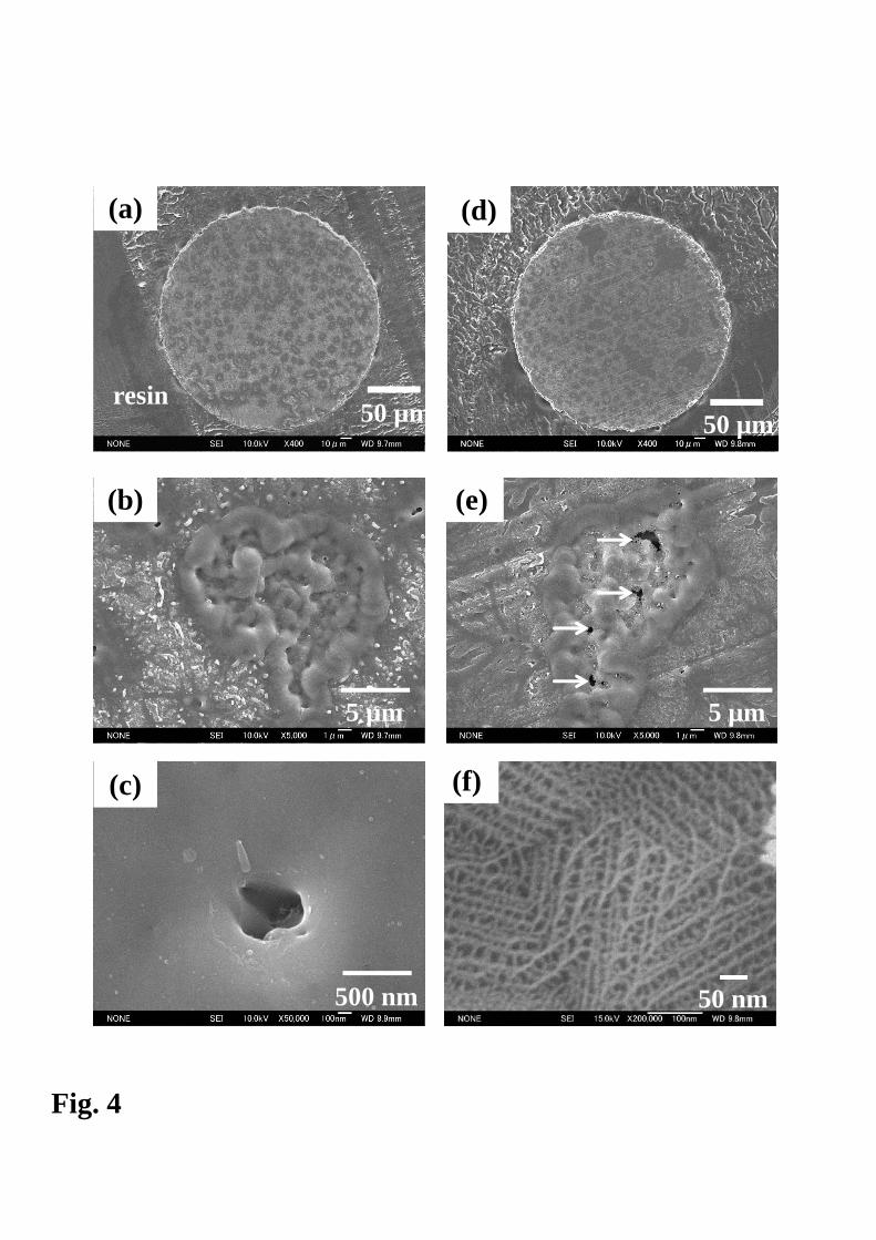
Fig. 4
(b)
(d)
50 µm
5 µm
(e)
50 nm
(f)
resin50 µm
(a)
(c)
5 µm
500 nm
(e)
Fig. 5
(a)
5 µm
Oxide film (c)
5 µm
Oxide film
(d)
5 µm
Metal surface(b)
5 µm
Metal surface
500 nm
(e)
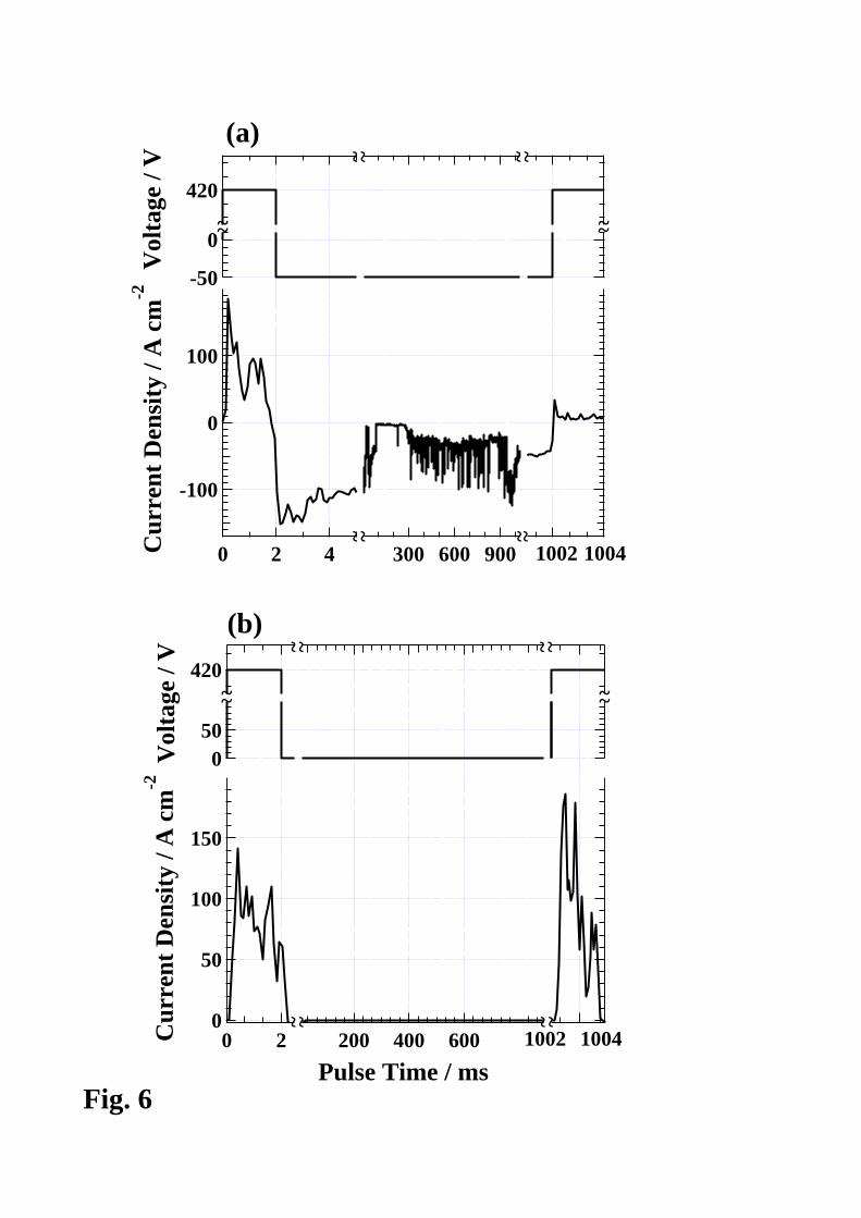
Fig. 6
(b)
(a)
150
100
50
0
Cu
rren
t D
ensi
ty /
A c
m-2
600400200
Pulse Time / ms20
500V
olta
ge /
V
420
~~~~
~~ ~~
1002 1004
~~ ~ ~
100
0
-100
Cu
rren
t D
ensi
ty /
A c
m-2
420
420
Vol
tage
/ V
-50
0
900600300 1002 1004
~ ~
~~~~
~ ~
~ ~~ ~
10 µm
(b)
Fig. 7
10 µm
(a)
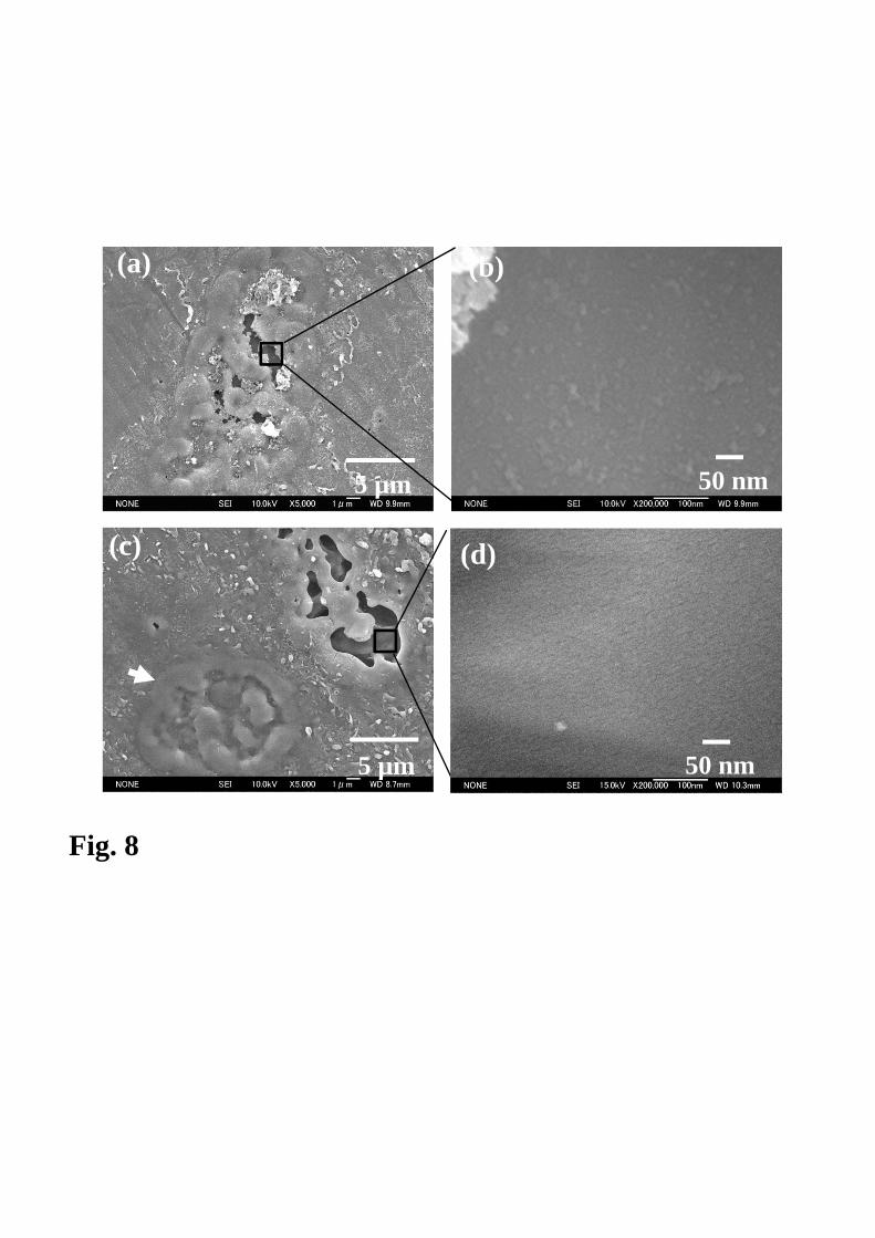
Fig. 8
(b)
50 nm
(a)
5 µm
(c)
5 µm
(d)
50 nm
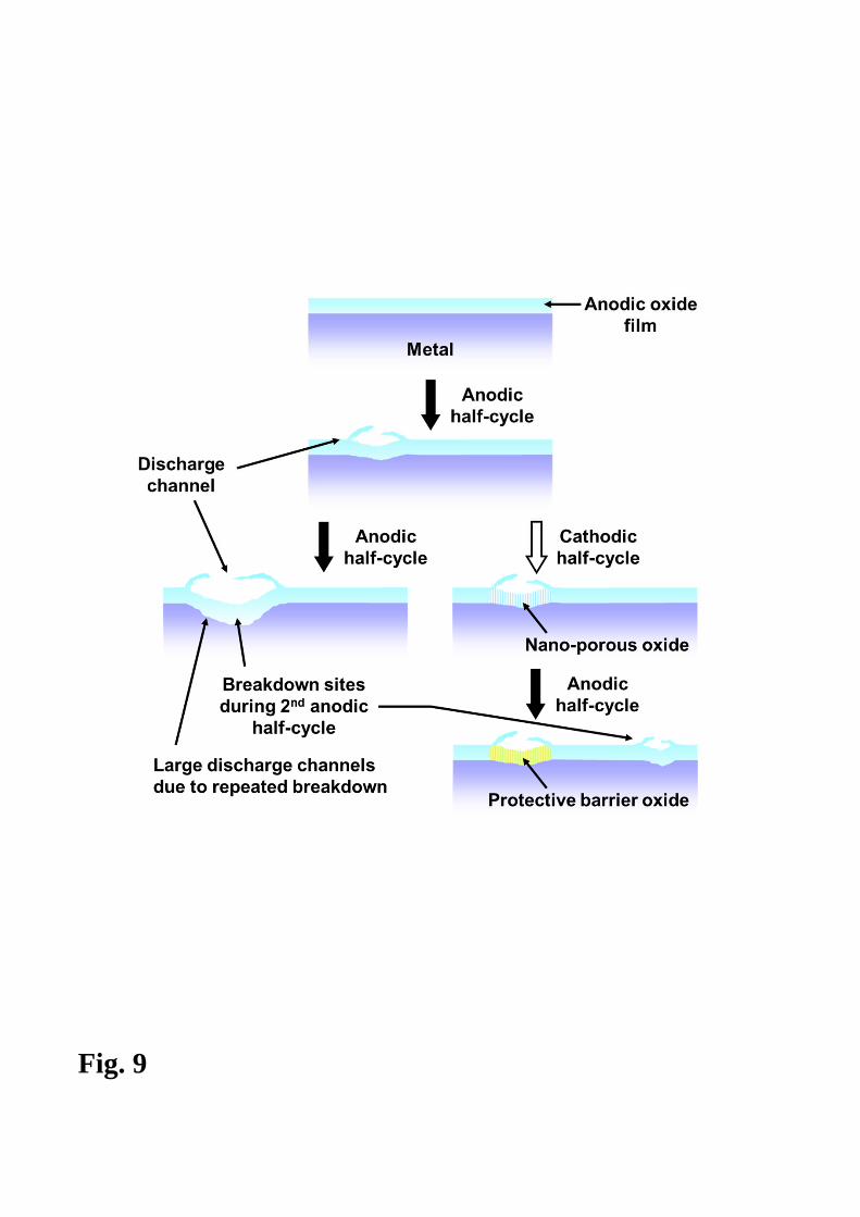
Fig. 9