Embed Size (px)
Citation preview
1
CCD Charge Injection Structure at Very SmallSignal Levels.
Gregory Prigozhin, Barry Burke, Marshall Bautz, Steve Kissel, Beverly LaMarr
Abstract—A frame transfer CCD designed for X-ray detectionon-board the SUZAKU spacecraft includes an input serial regis-ter and a charge injection structure which allows a very uniforminjection of extremely small charge packets into the imagingsection of the device. A variation of the fill-and-spill methodwas implemented to inject charge into the CCD. Very smallcharge packets (down to just a few electrons) can be reproduciblyinjected with noise as low as 5 electrons rms. The operationof the structure is described, and results of the measurementsare compared with the simulations. We have measured electron“evaporation” over potential barrier as a function of time, resultsbeing in excellent agreement with our model. By fitting a modelto the data it is possible to determine internal capacitance of theinput node. Charge injection noise as a function of signal chargewas measured, and the results are also in agreement with theory.The designed structure can be used as a tool for studying andmitigating radiation damage effects in CCDs.
Index Terms—X-ray, charge coupled device, active pixel sensor,charge injection, kTC noise
I. INTRODUCTION
Charge-Coupled Devices (CCDs) on high resistivity sub-strates have become detectors of choice for almost all soft X-ray space-based cameras performing imaging and spectroscopyin high-energy astrophysics. Several generations of X-raytelescopes, beginning with ASCA, progressing to the ChandraX-ray Telescope, XMM-Newton, SWIFT, and, most recently,SUZAKU carry on-board instruments based on such CCDsensors.
The space environment is known to be harmful for thesedetectors - high energy particles found there in high abundancegenerate defects in the crystal lattice of silicon. These defectsform traps for carriers that can capture signal electrons (n-channel devices will be considered here) and release them at alater time when the signal charge has already been transferredto a different pixel. Accumulation of such defects leads togradual deterioration of device performance due to increaseof charge transfer inefficiency (CTI).
We have shown previously [1] that periodic injection ofrows filled with “sacrificial charge” into a damaged arraymay improve device performance. Electrons from these rowsfill the traps, and the traps stay full for some time after the“sacrificial charge” packet leaves the pixel. So, when the signalcharge packet arrives, filled traps do not contribute to thecharge loss. In order to implement this technique, a new CCDchip, CCID-41, was designed for an X-ray camera on-board
G. Prigozhin, M. Bautz, S. Kissel, B. LaMarr are with Kavli Institute forAstrophysics at the Massachusetts Institute of Technology
Barry Burke is with Lincoln Laboratory at the Massachusetts Institute ofTechnology
the SUZAKU mission. SUZAKU was launched in July of2005 by the Institute of Space and Astronautical Sciences ofJapan’s Aerospace Exploration Agency (JAXA) and carriesinstruments developed by JAXA and NASA. The new chip issimilar to the CCID-17 device [2] originally developed at MITLincoln Laboratory for the ACIS instrument of the ChandraX-ray Observatory, but it was modified to include a chargeinjection structure and a serial register at the top of the imagingarray. The details of the design are discussed in section II.
The challenge here was to design a structure that wouldallow injection of very small charge packets with a very highreproducibility. CCDs for soft X-ray detection typically dealwith miniscule charge packets, sometimes only few hundredelectrons. In order to prevent trapping of the signal electrons,the injected packets should be just a little larger than thepackets generated by X-rays. Otherwise, a large injected signalwill reemit substantial numbers of electrons back into thepixels after passing through them and increase the noise level.Reemitted charge is somewhat similar to dark current and, ofcourse, needs to be minimized.
Key parameters of charge injection process were discussedin early work [3]–[5], but they were investigated for relativelylarge signals. Recently, several papers on the subject were pub-lished, showing a renewed interest in both experimental [6],[7] and theoretical aspects [8] of the regime of extremely smallcharge packets. Also, it is interesting to note that numerouspublications in the last few years discussed noise and chargelag of an Active Pixel Sensor (APS) in a subthreshold resetregime [9], [10]. This is the same process described by thesame equations as the spill phase of the charge injection. Wefind that the model used in [9], [10] is not adequate at verysmall signal levels and present both the theoretical formulationand comparison to experimental results in section III. Fittingthe model to the experimental data allowed us to measureinternal capacitance of the injection node, and that, in turn,can be used to evaluate kTC noise contribution at signal levelsthat are difficult to achieve by other means.
Testing in the lab and in flight indicates that charge injectionworks as intended mitigating the effects of proton irradiation.In addition, an ability to inject very uniformly controlledamount of charge opens up several unique opportunities formeasuring characteristics of the radiation damaged CCD.Some of the results of such tests were described in ourearlier work [7], [11], a more detailed paper will be publishedsoon. In section IV we describe briefly an example of usingcharge injection for characterization of the column-to-columnnonuniformity in radiation damaged CCDs. However, the mainfocus of this work is the operation and basic properties of the
2
charge injection circuit itself.
II. CHARGE INJECTION STRUCTURE
A simple solution for a charge injection structure is toplace an injecting diode, separated by a control gate, alongthe top of the imaging array. This would allow simultaneousinjection into all the columns of the device, thus being a fastway to inject charge. A very serious disadvantage of such anapproach, implemented in [6], is inevitable column-to-columnnonuniformity of the injected charge. In addition to the vari-ations caused by geometry fluctuations in different columns,there would be additional variations caused by differences intime delays in the signal propagation along the polysilicongates of such an injection structure.
In order to achieve very high uniformity of the injected sig-nal, a somewhat more complicated scheme was implementedhere – a single injection structure that injects charge into theserial register placed at the top of the imaging section. In thiscase charge injection to fill an entire row takes significantlylonger, but, since charge is always injected into the same inputstructure, pixel-to-pixel variability is minimized.
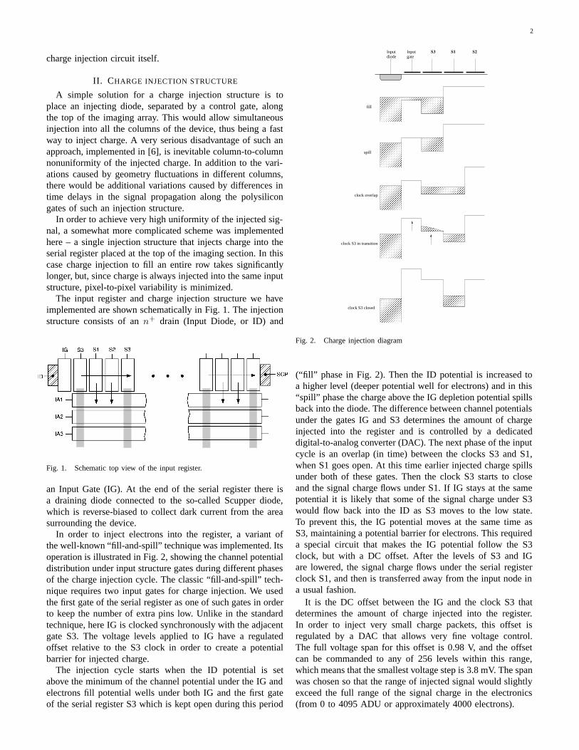
The input register and charge injection structure we haveimplemented are shown schematically in Fig. 1. The injectionstructure consists of an n+ drain (Input Diode, or ID) and
Fig. 1. Schematic top view of the input register.
an Input Gate (IG). At the end of the serial register there isa draining diode connected to the so-called Scupper diode,which is reverse-biased to collect dark current from the areasurrounding the device.
In order to inject electrons into the register, a variant ofthe well-known “fill-and-spill” technique was implemented. Itsoperation is illustrated in Fig. 2, showing the channel potentialdistribution under input structure gates during different phasesof the charge injection cycle. The classic “fill-and-spill” tech-nique requires two input gates for charge injection. We usedthe first gate of the serial register as one of such gates in orderto keep the number of extra pins low. Unlike in the standardtechnique, here IG is clocked synchronously with the adjacentgate S3. The voltage levels applied to IG have a regulatedoffset relative to the S3 clock in order to create a potentialbarrier for injected charge.
The injection cycle starts when the ID potential is setabove the minimum of the channel potential under the IG andelectrons fill potential wells under both IG and the first gateof the serial register S3 which is kept open during this period
Inputdiode
Inputgate
������������������������������
������������������������������
���������������
���������������
������������������������������
������������������������������
��������������������
������������������������������
������������������������������
��������������������������������������������
������������������������������
������������������������������
��������������������
��������������������
������������������������������������������������������������������������������������������
������������������������������������������������������������������������������������������
��������������������
clock overlap
spill
fill
S3 S1 S2
clock S3 in transition
clock S3 closed
Fig. 2. Charge injection diagram
(“fill” phase in Fig. 2). Then the ID potential is increased toa higher level (deeper potential well for electrons) and in this“spill” phase the charge above the IG depletion potential spillsback into the diode. The difference between channel potentialsunder the gates IG and S3 determines the amount of chargeinjected into the register and is controlled by a dedicateddigital-to-analog converter (DAC). The next phase of the inputcycle is an overlap (in time) between the clocks S3 and S1,when S1 goes open. At this time earlier injected charge spillsunder both of these gates. Then the clock S3 starts to closeand the signal charge flows under S1. If IG stays at the samepotential it is likely that some of the signal charge under S3would flow back into the ID as S3 moves to the low state.To prevent this, the IG potential moves at the same time asS3, maintaining a potential barrier for electrons. This requireda special circuit that makes the IG potential follow the S3clock, but with a DC offset. After the levels of S3 and IGare lowered, the signal charge flows under the serial registerclock S1, and then is transferred away from the input node ina usual fashion.
It is the DC offset between the IG and the clock S3 thatdetermines the amount of charge injected into the register.In order to inject very small charge packets, this offset isregulated by a DAC that allows very fine voltage control.The full voltage span for this offset is 0.98 V, and the offsetcan be commanded to any of 256 levels within this range,which means that the smallest voltage step is 3.8 mV. The spanwas chosen so that the range of injected signal would slightlyexceed the full range of the signal charge in the electronics(from 0 to 4095 ADU or approximately 4000 electrons).
3
If the potential of the ID during the injection cycle is setto a high positive level no charge will flow into the CCD.Thus, disabling the ID switching to low level at certain clockcycles allowed us to produce any desired pattern of injectedpixels. The IG offset (and, hence, amount of injected charge)was kept the same for all the pixels in a given frame.
III. CHARGE INJECTION RESULTS AND DISCUSSION
A. Measurement procedure and charge as a function of volt-age
To study the parameters of the injection structure we madescans of the IG offset so that the injected charge changed from0 to the level where saturation of the readout ADC was reached(this level corresponds to a few thousand electrons in a CCDpotential well). For each value of the IG offset 15 framesof identical data were taken to improve the accuracy of theresult. We used a specific pattern of the injected pixels to avoidthe distortion of measurement results by the CTI. Each framehad eight sequential rows of pixels containing injected charge.These rows with injected charge were transferred through theentire array to the bottom of the frame store section at a speedof 24 µs/transfer (strictly speaking the first injected row was10 rows away from the serial register after this transfer). Thenthe frame store section was read out in a regular mode throughthe serial registers. The rest of the pixels in the frame, exceptfor the eight injected rows, were empty.
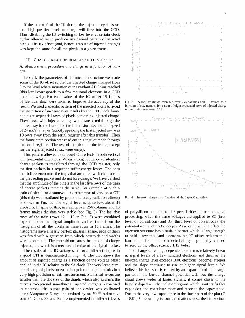
This pattern allowed us to avoid CTI effects in both verticaland horizontal directions. When a long sequence of identicalcharge packets is transferred through the CCD register, onlythe first packets in a sequence suffer charge losses. The onesthat follow encounter the traps that are filled with electrons ofthe preceeding packet and do not lose charge. We have verifiedthat the amplitude of the pixels in the last five rows of the trainof charge packets remains the same. An example of such atrain of pixels for a somewhat extreme case of very poor CTI(this chip was irradiated by protons to study radiation effects)is shown in Fig. 3. The signal level is quite low, about 34electrons. In spite of this, averaging over 256 columns and 15frames makes the data very stable (see Fig. 3). The last fiverows of the train (rows 12 – 16 in Fig. 3) were combinedtogether to extract signal amplitude and variance from thehistogram of all the pixels in these rows in 15 frames. Thehistograms have a nearly perfect gaussian shape, each of themwas fitted with a gaussian from which centroids and widthswere determined. The centroid measures the amount of chargeinjected, the width is a measure of noise of the signal packet.
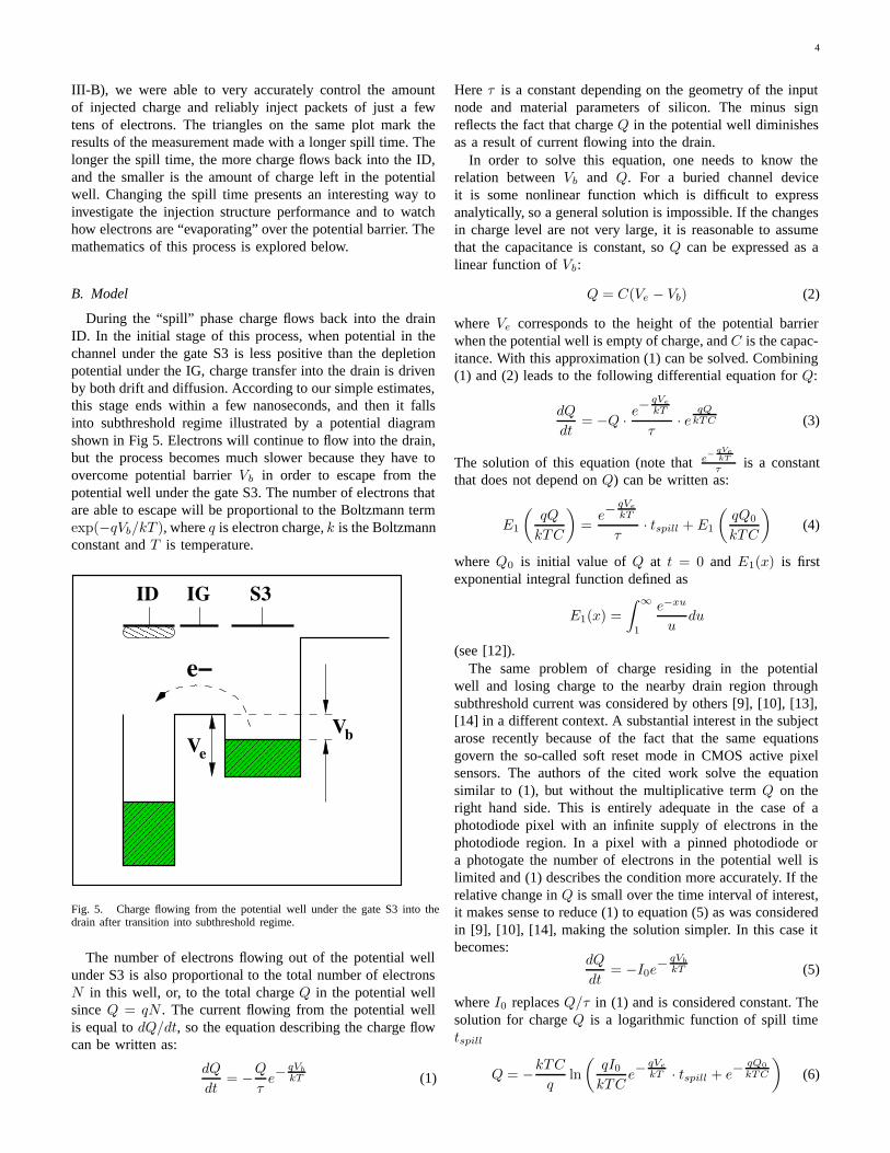
The results of the IG voltage scan for a different chip witha good CTI is demonstrated in Fig. 4. The plot shows theamount of injected charge as a function of the voltage offsetapplied to the IG relative to the S3 clock. The very large num-ber of sampled pixels for each data point in the plot results in avery high precision of this measurement. Statistical errors aresmaller than the dot size of the graph, which also explains thecurve’s exceptional smoothness. Injected charge is expressedin electrons (the output gain of the device was calibratedusing Manganese X-ray line emitted by an Fe55 radioactivesource). Gates S3 and IG are implemented in different levels
Fig. 3. Signal amplitude averaged over 256 columns and 15 frames as afunction of row number for a train of eight sequential rows of injected chargein the proton irradiated CCD.
Fig. 4. Injected charge as a function of the Input Gate offset.
of polysilicon and due to the peculiarities of technologicalprocessing, when the same voltages are applied to S3 (firstlevel of polysilicon) and IG (third level of polysilicon), thepotential well under S3 is deeper. As a result, with no offset theinjection structure has a built-in barrier which is large enoughto hold a few thousand electrons. An IG offset reduces thisbarrier and the amount of injected charge is gradually reducedto zero as the offset reaches 1.15 Volts.
The charge-vs-voltage dependence remains relatively linearat signal levels of a few hundred electrons and then, as theinjected charge level exceeds 1000 electrons, becomes steeperand the slope continues to rise at higher signal levels. Webelieve this behavior is caused by an expansion of the chargepacket in the buried channel potential well. As the chargecloud grows wider at larger signals, it comes closer to theheavily doped p+ channel-stop regions which limit its furtherexpansion and contribute more and more to the capacitance.Due to the very low capacitance in the linear part of the plot (C= 0.81fF according to our calculations described in section
4
III-B), we were able to very accurately control the amountof injected charge and reliably inject packets of just a fewtens of electrons. The triangles on the same plot mark theresults of the measurement made with a longer spill time. Thelonger the spill time, the more charge flows back into the ID,and the smaller is the amount of charge left in the potentialwell. Changing the spill time presents an interesting way toinvestigate the injection structure performance and to watchhow electrons are “evaporating” over the potential barrier. Themathematics of this process is explored below.
B. Model
During the “spill” phase charge flows back into the drainID. In the initial stage of this process, when potential in thechannel under the gate S3 is less positive than the depletionpotential under the IG, charge transfer into the drain is drivenby both drift and diffusion. According to our simple estimates,this stage ends within a few nanoseconds, and then it fallsinto subthreshold regime illustrated by a potential diagramshown in Fig 5. Electrons will continue to flow into the drain,but the process becomes much slower because they have toovercome potential barrier Vb in order to escape from thepotential well under the gate S3. The number of electrons thatare able to escape will be proportional to the Boltzmann termexp(−qVb/kT ), where q is electron charge, k is the Boltzmannconstant and T is temperature.
����������������
����������������
������������
������������
e−
S3IGID
VVb
e
Fig. 5. Charge flowing from the potential well under the gate S3 into thedrain after transition into subthreshold regime.
The number of electrons flowing out of the potential wellunder S3 is also proportional to the total number of electronsN in this well, or, to the total charge Q in the potential wellsince Q = qN . The current flowing from the potential wellis equal to dQ/dt, so the equation describing the charge flowcan be written as:
dQ
dt= −Q
τe−
qVb
kT (1)
Here τ is a constant depending on the geometry of the inputnode and material parameters of silicon. The minus signreflects the fact that charge Q in the potential well diminishesas a result of current flowing into the drain.
In order to solve this equation, one needs to know therelation between Vb and Q. For a buried channel deviceit is some nonlinear function which is difficult to expressanalytically, so a general solution is impossible. If the changesin charge level are not very large, it is reasonable to assumethat the capacitance is constant, so Q can be expressed as alinear function of Vb:
Q = C(Ve − Vb) (2)
where Ve corresponds to the height of the potential barrierwhen the potential well is empty of charge, and C is the capac-itance. With this approximation (1) can be solved. Combining(1) and (2) leads to the following differential equation for Q:
dQ
dt= −Q · e−
qVe
kT
τ· e
qQkTC (3)
The solution of this equation (note that e− qVe
kT
τ is a constantthat does not depend on Q) can be written as:
E1
kTC
)=
e−qVe
kT
τ· tspill + E1
(qQ0
kTC
)(4)
where Q0 is initial value of Q at t = 0 and E1(x) is firstexponential integral function defined as
E1(x) =∫ ∞
1
e−xu
udu
(see [12]).The same problem of charge residing in the potential
well and losing charge to the nearby drain region throughsubthreshold current was considered by others [9], [10], [13],[14] in a different context. A substantial interest in the subjectarose recently because of the fact that the same equationsgovern the so-called soft reset mode in CMOS active pixelsensors. The authors of the cited work solve the equationsimilar to (1), but without the multiplicative term Q on theright hand side. This is entirely adequate in the case of aphotodiode pixel with an infinite supply of electrons in thephotodiode region. In a pixel with a pinned photodiode ora photogate the number of electrons in the potential well islimited and (1) describes the condition more accurately. If therelative change in Q is small over the time interval of interest,it makes sense to reduce (1) to equation (5) as was consideredin [9], [10], [14], making the solution simpler. In this case itbecomes:
dQ
dt= −I0e
− qVb
kT (5)
where I0 replaces Q/τ in (1) and is considered constant. Thesolution for charge Q is a logarithmic function of spill timetspill
Q = −kTC
qln
(qI0
kTCe−
qVe
kT · tspill + e−qQ0kTC
)(6)
5
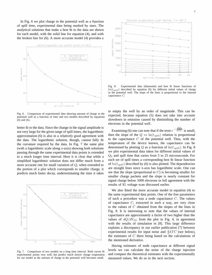
In Fig. 6 we plot charge in the potential well as a functionof spill time, experimental data being marked by stars. Theanalytical solutions that make a best fit to the data are shownfor each model, with the solid line for equation (4), and withthe broken line for (6). A more accurate model (4) provides a
Fig. 6. Comparison of experimental data showing amount of charge in thepotential well as a function of time and two models described by equations(4) and (6).
better fit to the data. Since the change in the signal amplitude isnot very large for the given range of spill times, the logarithmicapproximation (6) is also in a relatively good agreement withthe data. The logarithmic solution, though, cannot fully fitthe curvature required by the data. In Fig. 7 the same plot(with a logarithmic scale along x-axis) showing both solutionspassing through the same experimental data points is extendedto a much longer time interval. Here it is clear that while asimplified logarithmic solution does not differ much from amore accurate one for small variation of Q, when extended tothe portion of a plot which corresponds to smaller charge, itpredicts much faster decay, underestimating the time it takes
Fig. 7. Comparison of two models on a long time interval. Both curves fitexperimental points very well, but predict much slower charge evaporationfor our model as the amount of charge in the potential well becomes small.
Fig. 8. Experimental data (diamonds) and best fit linear functions ofln(tspill) described by equation (6) for different initial values of chargein the potential well. The slope of the lines is proportional to the internalcapacitance C.
to empty the well by an order of magnitude. This can beexpected, because equation (5) does not take into accountslowdown in emission caused by diminishing the number ofelectrons in the potential well.
Examining (6) one can note that if the term e−qQ0kTC is small,
then the slope of the Q vs ln(tspill) relation is proportionalto the capacitance C of the potential well. Thus, with thetemperature of the device known, the capacitance can bedetermined by plotting Q as a function of ln(tspill). In Fig. 8we plot experimental data taken for different initial values ofQ0 and spill time that varies from 5 to 25 microseconds. Foreach set of spill times a corresponding best fit linear functionof ln(tspill) described by (6) is also plotted. The dependenciesare straight lines since x-axis has logarithmic scale. One cansee that the slope (proportional to C) is becoming smaller forsmaller charge packets and the slope is nearly constant forsignal charge below 1000 electrons in full agreement with theresults of IG voltage scan discussed earlier.
We also fitted the more accurate model in equation (4) tothe same experimental data points. One of the free parametersof such a procedure was a node capacitance C. The valuesof capacitance C, extracted in such a way, are very closeto the values of C obtained from the slopes of the lines inFig. 8. It is interesting to note that the values of internalcapacitance are approximately a factor of two higher than thevalues of dQ/dVIG from the plot in Fig. 4, in agreementwith the results of simulation in [8]. This large differenceexplains a discrepancy in our earlier publication [7] betweenexperimental results for input noise and 1
2kTC (see below),the estimates of C there being based on the calculations ofthe mentioned derivative.
Having estimates of node capacitance at different signallevels we can calculate the noise of the charge injectionand compare the theoretical estimates with the experimentallymeasured values. We do so in the next section.
6
Fig. 9. Noise of the injected charge as a function of Input Gate offset fortwo different spill times.
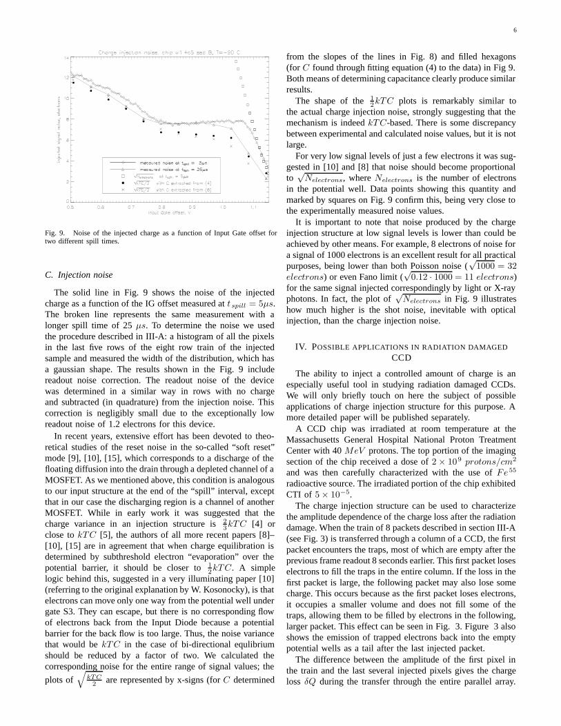
C. Injection noise
The solid line in Fig. 9 shows the noise of the injectedcharge as a function of the IG offset measured at tspill = 5µs.The broken line represents the same measurement with alonger spill time of 25 µs. To determine the noise we usedthe procedure described in III-A: a histogram of all the pixelsin the last five rows of the eight row train of the injectedsample and measured the width of the distribution, which hasa gaussian shape. The results shown in the Fig. 9 includereadout noise correction. The readout noise of the devicewas determined in a similar way in rows with no chargeand subtracted (in quadrature) from the injection noise. Thiscorrection is negligibly small due to the exceptionally lowreadout noise of 1.2 electrons for this device.
In recent years, extensive effort has been devoted to theo-retical studies of the reset noise in the so-called “soft reset”mode [9], [10], [15], which corresponds to a discharge of thefloating diffusion into the drain through a depleted channel of aMOSFET. As we mentioned above, this condition is analogousto our input structure at the end of the “spill” interval, exceptthat in our case the discharging region is a channel of anotherMOSFET. While in early work it was suggested that thecharge variance in an injection structure is 2
3kTC [4] orclose to kTC [5], the authors of all more recent papers [8]–[10], [15] are in agreement that when charge equilibration isdetermined by subthreshold electron “evaporation” over thepotential barrier, it should be closer to 1
2kTC. A simplelogic behind this, suggested in a very illuminating paper [10](referring to the original explanation by W. Kosonocky), is thatelectrons can move only one way from the potential well undergate S3. They can escape, but there is no corresponding flowof electrons back from the Input Diode because a potentialbarrier for the back flow is too large. Thus, the noise variancethat would be kTC in the case of bi-directional equlibriumshould be reduced by a factor of two. We calculated thecorresponding noise for the entire range of signal values; the
plots of√
kTC2 are represented by x-signs (for C determined
from the slopes of the lines in Fig. 8) and filled hexagons(for C found through fitting equation (4) to the data) in Fig 9.Both means of determining capacitance clearly produce similarresults.
The shape of the 12kTC plots is remarkably similar to
the actual charge injection noise, strongly suggesting that themechanism is indeed kTC-based. There is some discrepancybetween experimental and calculated noise values, but it is notlarge.
For very low signal levels of just a few electrons it was sug-gested in [10] and [8] that noise should become proportionalto
√Nelectrons, where Nelectrons is the number of electrons
in the potential well. Data points showing this quantity andmarked by squares on Fig. 9 confirm this, being very close tothe experimentally measured noise values.
It is important to note that noise produced by the chargeinjection structure at low signal levels is lower than could beachieved by other means. For example, 8 electrons of noise fora signal of 1000 electrons is an excellent result for all practicalpurposes, being lower than both Poisson noise (
√1000 = 32
electrons) or even Fano limit (√
0.12 · 1000 = 11 electrons)for the same signal injected correspondingly by light or X-rayphotons. In fact, the plot of
√Nelectrons in Fig. 9 illustrates
how much higher is the shot noise, inevitable with opticalinjection, than the charge injection noise.
IV. POSSIBLE APPLICATIONS IN RADIATION DAMAGED
CCD
The ability to inject a controlled amount of charge is anespecially useful tool in studying radiation damaged CCDs.We will only briefly touch on here the subject of possibleapplications of charge injection structure for this purpose. Amore detailed paper will be published separately.
A CCD chip was irradiated at room temperature at theMassachusetts General Hospital National Proton TreatmentCenter with 40 MeV protons. The top portion of the imagingsection of the chip received a dose of 2 × 10⁹ protons/cm2
and was then carefully characterized with the use of Fe55
radioactive source. The irradiated portion of the chip exhibitedCTI of 5 × 10⁻⁵.
The charge injection structure can be used to characterizethe amplitude dependence of the charge loss after the radiationdamage. When the train of 8 packets described in section III-A(see Fig. 3) is transferred through a column of a CCD, the firstpacket encounters the traps, most of which are empty after theprevious frame readout 8 seconds earlier. This first packet loseselectrons to fill the traps in the entire column. If the loss in thefirst packet is large, the following packet may also lose somecharge. This occurs because as the first packet loses electrons,it occupies a smaller volume and does not fill some of thetraps, allowing them to be filled by electrons in the following,larger packet. This effect can be seen in Fig. 3. Figure 3 alsoshows the emission of trapped electrons back into the emptypotential wells as a tail after the last injected packet.
The difference between the amplitude of the first pixel inthe train and the last several injected pixels gives the chargeloss δQ during the transfer through the entire parallel array.
7
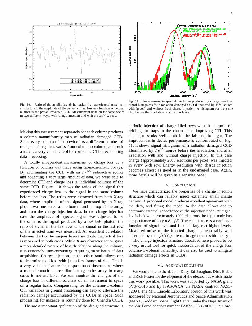
Fig. 10. Ratio of the amplitudes of the packet that experienced maximumcharge loss to the amplitude of the packet with no loss as a function of columnnumber in the proton irradiated CCD. Measurement done on the same devicein two different ways: with charge injection and with 5.9 keV X-rays.
Making this measurement separately for each column producesa column nonuniformity map of radiation damaged CCD.Since every column of the device has a different number oftraps, the charge loss varies from column to column, and sucha map is a very valuable tool for correcting CTI effects duringdata processing.
A totally independent measurement of charge loss as afunction of column was made using monochromatic X-rays.By illuminating the CCD with an Fe55 radioactive sourceand collecting a very large amount of data, we were able todetermine CTI and charge loss in individual columns of thesame CCD. Figure 10 shows the ratios of the signal thatexperienced charge loss to the signal in the same columnbefore the loss. The ratios were extracted from both X-raydata, where amplitude of the signal generated by an X-rayphoton was measured at the bottom and the top of the array,and from the charge injection data. In the charge injectioncase the amplitude of injected signal was adjusted to bethe same as the signal produced by a 5.9 keV photon; theratio of signal in the first row to the signal in the last rowof the injected train was measured. An excellent correlationbetween the two techniques leaves no doubt that actual lossis measured in both cases. While X-ray characterization givesa more detailed picture of loss distribution along the column,it is extremely time-consuming, requiring many hours of dataacquisition. Charge injection, on the other hand, allows oneto determine total loss with just a few frames of data. This isa very valuable feature for a space-based instrument, wherea monochromatic source illuminating entire array in manycases is not available. We can monitor the changes of thecharge loss in different columns of an instrument in spaceon a regular basis. Compensating for the column-to-columnCTI variations in ground processing can help to alleviate theradiation damage accumulated by the CCDs in space. Suchprocessing, for instance, is routinely done for Chandra CCDs.
The most important application of the designed structure is
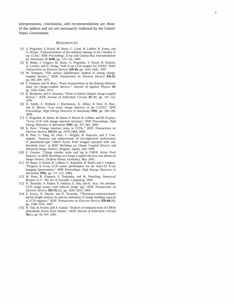
Fig. 11. Improvement in spectral resolution produced by charge injection.Signal histograms for a radiation damaged CCD illuminated by Fe55 sourcewith (green) and without (red) charge injection. A histogram for the samechip before the irradiation is shown in black.
periodic injection of charge-filled rows with the purpose ofrefilling the traps in the channel and improving CTI. Thistechnique works well, both in the lab and in flight. Theimprovement in device performance is demonstrated on Fig.11. It shows signal histograms of a radiation damaged CCDilluminated by Fe55 source before the irradiation, and afterirradiation with and without charge injection. In this casecharge (approximately 2000 electrons per pixel) was injectedin every 54th row. Energy resolution with charge injectionbecomes almost as good as in the undamaged case. Again,more details will be given in a separate paper.
V. CONCLUSION
We have characterized the properties of a charge injectionstructure which can reliably inject extremely small chargepackets. A proposed model produces excellent agreement withthe data, and fitting the model to the data allows one todetermine internal capacitance of the injection node. At signallevels below approximately 1000 electrons the input node hasa capacitance of only 0.81 fF . The capacitance is a nonlinearfunction of signal level and is much larger at higher levels.Measured noise of the injected charge is reasonably welldescribed by the
√kTC/2 term, in agreement with theory.
The charge injection structure described here proved to bea very useful tool for quick measurement of the charge losscolumn-to-column variability. It can also be used to mitigateradiation damage effects in CCDs.
VI. ACKNOWLEDGMENTS
We would like to thank John Doty, Ed Boughan, Dick Elder,and Rick Foster for development of the electronics which madethis work possible. This work was supported by NASA grantSV3-73016 and by ISAS/JAXA via NASA contract NAS5-02094. The MIT Lincoln Laboratory portion of this work wassponsored by National Aeronautics and Space Administration(NASA) Goddard Space Flight Center under the Department ofthe Air Force contract number FA8721-05-C-0002. Opinions,
8
interpretations, conclusions, and recommendations are thoseof the authors and are not necessarily endorsed by the UnitedStates Government.
REFERENCES
[1] G. Prigozhin, S. Kissel, M. Bautz, C. Grant, B. LaMarr, R. Foster, andG. Ricker, “Characterization of the radiation damage in the Chandra X-ray CCDs,” SPIE Proceedings, X-ray and Gamma-Ray Instrumentationfor Astronomy XI 4140, pp. 123–134, 2000.
[2] B. Burke, J. Gregory, M. Bautz, G. Prigozhin, S. Kissel, B. Kosicki,A. Loomis, and D. Young, “Soft X-ray CCD imagers for AXAF,” IEEETransactions on Electron Devices ED-44, pp. 1633–1642, 1997.
[3] M. Tompsett, “The surface equilibration method of setting charge-coupled devices.,” IEEE Transactions on Electron Devices ED-22,pp. 305–309, 1975.
[4] S. Emmons and D. Buss, “Noise measurement on the floating diffusioninput for charge-coupled devices.,” Journal of Applied Physics 45,pp. 5303–5306, 1974.
[5] R. Brodersen and S. Emmons, “Noise in buried channel charge-coupleddevices.,” IEEE Journal of Solid-State Circuits SC-11, pp. 147–155,1976.
[6] D. Smith, A. Holland, I. Hutchinson, A. Abbey, P. Pool, D. Burt,and D. Morris, “Low noise charge injection in the CCD22,” SPIEProceedings, High Energy Detectors in Astronomy 5501, pp. 189–196,2004.
[7] G. Prigozhin, B. Burke, M. Bautz, S. Kissel, B. LaMarr, and M. Freytsis,“X-ray CCD with charge injection structure,” SPIE Proceedings, HighEnergy Detectors in Astronomy 5501, pp. 357–365, 2004.
[8] B. Kern, “Charge injection noise in CCDs.,” IEEE Transactions onElectron Devices ED-53, pp. 2478–2484, 2006.
[9] B. Pain, G. Yang, M. Ortiz, C. Wrigley, B. Hancock, and T. Cun-ingham, “Analysis and enhancement of low-light-level performanceof photodiode-type CMOS Active Pixel Imagers operated with sub-threshold reset,” in IEEE Workshop on Charge Coupled Devices andAdvanced Image Sensors, (Nagano, Japan), June 1999.
[10] E. Fossum, “Charge transfer noise and lag in CMOS Active PixelSensors,” in IEEE Workshop on Charge Coupled Devices and AdvancedImage Sensors, (Schloss Elmau, Germany), May 2003.
[11] M. Bautz, S. Kissel, B. LaMarr, G. Prigozhin, B. Burke, and J. Gregory,“Progress in X-ray CCD sensor performance for the Astro-E2 X-rayImaging Spectrometer,” SPIE Proceedings, High Energy Detectors inAstronomy 5501, pp. 111–122, 2004.
[12] W. Press, B. Flannery, S. Teukolsky, and W. Vetterling, NumericalRecipes in C: The Art of Scientific Computing, 1990.
[13] N. Teranishi, A. Kohno, Y. Ishihara, E. Oda, and K. Arai, “An interlineCCD image sensor with reduced image lag,” IEEE Transactions onElectron Devices ED-31(12), pp. 1829–1833, 1984.
[14] S. Kawai, N. Mutoh, and N. Teranishi, “Thermionic-emission-basedbarrier height analysis for precise estimation of charge handling capacityin CCD registers,” IEEE Transactions on Electron Devices ED-44(10),pp. 1588–1592, 1997.
[15] H. Tian, B. Fowler, and A. Gamal, “Analysis of temporal noise in CMOSphotodiode Active Pixel Sensor.,” IEEE Journal of Solid-State Circuits36(1), pp. 92–101, 2001.