Embed Size (px)
Citation preview
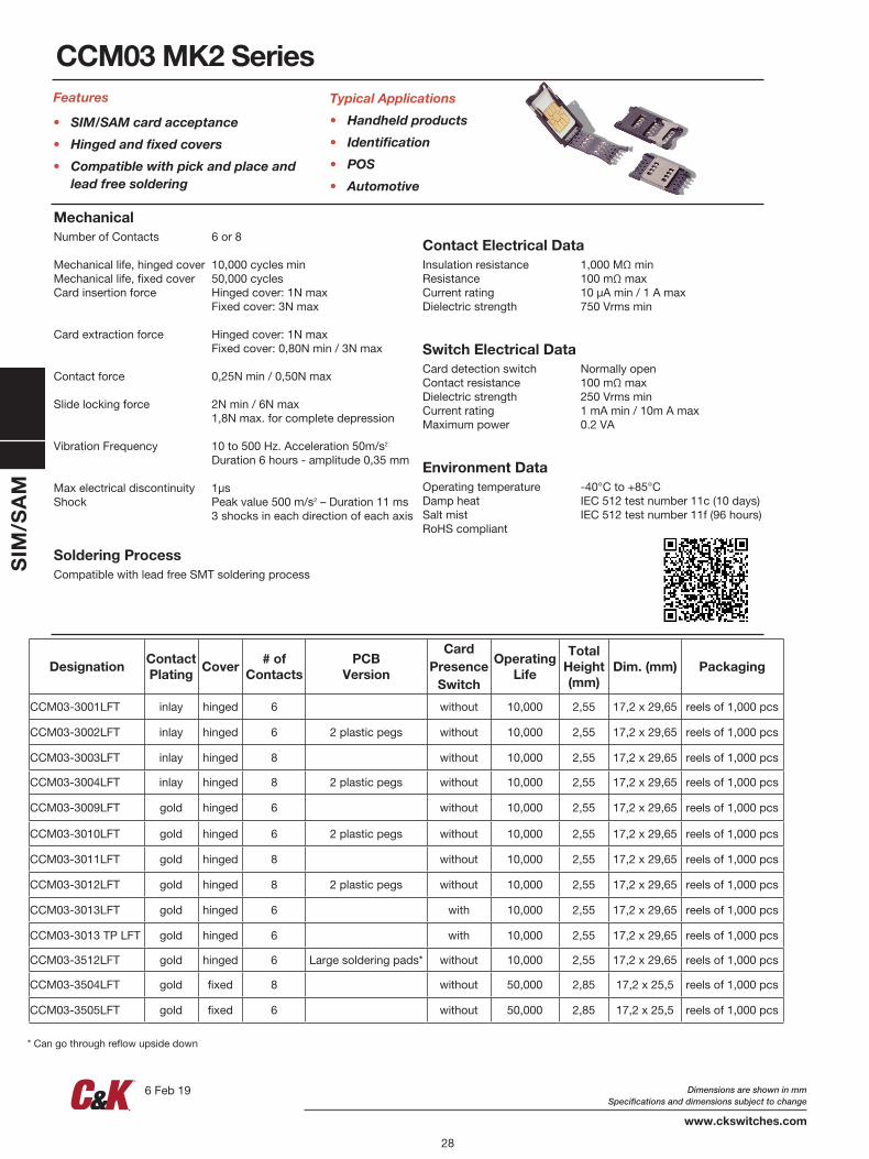
DesignationContact Plating
Cover# of
ContactsPCB
Version
CardPresence
Switch
Operating Life
Total Height (mm)
Dim. (mm) Packaging
CCM03-3001LFT inlay hinged 6 without 10,000 2,55 17,2 x 29,65 reels of 1,000 pcs
CCM03-3002LFT inlay hinged 6 2 plastic pegs without 10,000 2,55 17,2 x 29,65 reels of 1,000 pcs
CCM03-3003LFT inlay hinged 8 without 10,000 2,55 17,2 x 29,65 reels of 1,000 pcs
CCM03-3004LFT inlay hinged 8 2 plastic pegs without 10,000 2,55 17,2 x 29,65 reels of 1,000 pcs
CCM03-3009LFT gold hinged 6 without 10,000 2,55 17,2 x 29,65 reels of 1,000 pcs
CCM03-3010LFT gold hinged 6 2 plastic pegs without 10,000 2,55 17,2 x 29,65 reels of 1,000 pcs
CCM03-3011LFT gold hinged 8 without 10,000 2,55 17,2 x 29,65 reels of 1,000 pcs
CCM03-3012LFT gold hinged 8 2 plastic pegs without 10,000 2,55 17,2 x 29,65 reels of 1,000 pcs
CCM03-3013LFT gold hinged 6 with 10,000 2,55 17,2 x 29,65 reels of 1,000 pcs
CCM03-3013 TP LFT gold hinged 6 with 10,000 2,55 17,2 x 29,65 reels of 1,000 pcs
CCM03-3512LFT gold hinged 6 Large soldering pads* without 10,000 2,55 17,2 x 29,65 reels of 1,000 pcs
CCM03-3504LFT gold fixed 8 without 50,000 2,85 17,2 x 25,5 reels of 1,000 pcs
CCM03-3505LFT gold fixed 6 without 50,000 2,85 17,2 x 25,5 reels of 1,000 pcs
SIM
/SA
M
MechanicalNumber of Contacts 6 or 8 Mechanical life, hinged cover 10,000 cycles min Mechanical life, fixed cover 50,000 cycles Card insertion force Hinged cover: 1N max Fixed cover: 3N max Card extraction force Hinged cover: 1N max Fixed cover: 0,80N min / 3N max Contact force 0,25N min / 0,50N max Slide locking force 2N min / 6N max 1,8N max. for complete depression Vibration Frequency 10 to 500 Hz. Acceleration 50m/s2 Duration 6 hours - amplitude 0,35 mm Max electrical discontinuity 1µs Shock Peak value 500 m/s2 – Duration 11 ms 3 shocks in each direction of each axis
Soldering Process
Compatible with lead free SMT soldering process
Contact Electrical DataInsulation resistance 1,000 MΩ min Resistance 100 mΩ max Current rating 10 µA min / 1 A max Dielectric strength 750 Vrms min
Switch Electrical DataCard detection switch Normally open Contact resistance 100 mΩ max Dielectric strength 250 Vrms min Current rating 1 mA min / 10m A max Maximum power 0.2 VA
Environment DataOperating temperature -40°C to +85°C Damp heat IEC 512 test number 11c (10 days) Salt mist IEC 512 test number 11f (96 hours) RoHS compliant
Features
• SIM/SAM card acceptance
• Hinged and fixed covers
• Compatible with pick and place and lead free soldering
Typical Applications
• Handheld products
• Identification
• POS
• Automotive
* Can go through reflow upside down
CCM03 MK2 Series
28
Dimensions are shown in mm Specifications and dimensions subject to change
www.ckswitches.com
6 Feb 19
29
SIM
/SA
M
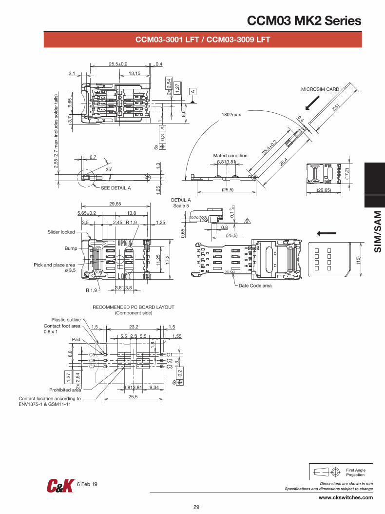
CCM03-3001 LFT / CCM03-3009 LFT
MICROSIM CARD
R 1,9
1,3
1,25
2,55
(2,7
max
. inc
lud
es s
old
er t
ails
)
11,2
5
17,2
3,81 3,8
3,5 2,45 1,25
5,65±0,2 13,8
29,65
(17,
2)
(29,65)
00,
1 -
0,1
0,7
25˚
0,8
(25,5)
9,65
0,65
2,1
25,5±0,2 0,4
13,15
R 1,9
2x2,
54
10,
3A
1,27
8,6
3,7
3,813,81
25,4
±0,2
0,4180?max
(25,5)
(25)
28,4
(15)
XX-XXX
SEE DETAIL A
Date Code area
Mated condition6x
Pick and place area ø 3,5
Slider locked
Bump
DETAIL AScale 5
A
2
1,27
8,6
23,2
25,5
2,5 5,55,5
1,3
0,2
3,813,81
1,8
1,5 1,5
9,342x2,
54
1,55
Contact location according to ENV1375-1 & GSM11-11
C5
Contact foot area 0,8 x 1
RECOMMENDED PC BOARD LAYOUT(Component side)
C6C7
C1C2C3
6x
Plastic outline
Pad
Prohibited area
Dimensions are shown in mm Specifications and dimensions subject to change
www.ckswitches.com
CCM03 MK2 Series
6 Feb 19
30
Dimensions are shown in mm Specifications and dimensions subject to change
www.ckswitches.com
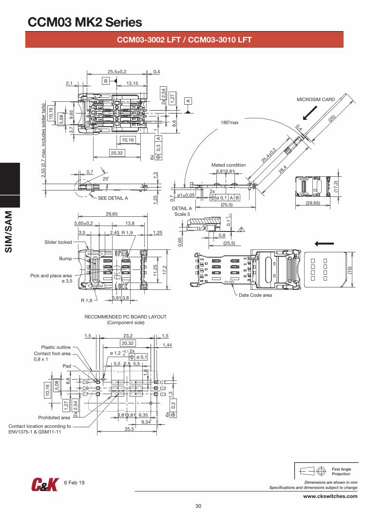
CCM03-3002 LFT / CCM03-3010 LFT
SIM
/SA
M
CCM03 MK2 Series
MICROSIM CARD
R 1,9
1,3
1,25
2,55
(2,7
max
. inc
lud
es s
old
er t
ails
)
11,2
5
17,2
3,81 3,8
3,5 2,45 1,25
5,65±0,2 13,8
29,65
(17,
2)
(29,65)
00,
1 -
0,1
0,7
25˚
0,8
(25,5)
R 1,9
9,65
2,1
25,5±0,2
13,15
0,4
2x2,
54
0,65
10,
3A10,16
20,32
10,1
6
5,08
8,6
1,27
3,7
3,813,81
25,4
±0,2
0,4180˚max
(25,5)
(25)
28,4
(15)
ø1±0,05 ø 0,1 A B0,7
XX-XXX
SEE DETAIL A
Date Code area
Mated condition
6x
2x
Pick and place area ø 3,5
Slider locked
Bump
DETAIL AScale 5
B
A
2
1,27
8,6
23,2
25,5
2,5 5,55,5
3,813,81
1,8
1,5 1,5
9,34
6,35
20,32
10,1
6
5,08
+0,1ø 1,2 0�ø 0,1
1,44
2x2,
54
1,3
0,2
Contact location according to ENV1375-1 & GSM11-11
Contact foot area 0,8 x 1
RECOMMENDED PC BOARD LAYOUT(Component side)
6x
C5
Plastic outline
Pad
Prohibited area
C6C7
C1C2C3
2x
6 Feb 19
31
Dimensions are shown in mm Specifications and dimensions subject to change
www.ckswitches.com
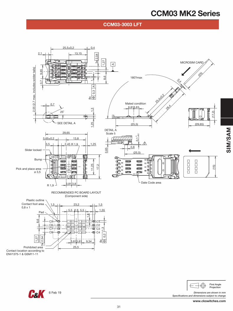
CCM03-3003 LFT
SIM
/SA
M
CCM03 MK2 Series
MICROSIM CARD
R 1,9
1,3
1,25
2,55
(2,7
max
. inc
lud
es s
old
er t
ails
)
11,2
5
17,2
3,81 3,8
3,5 2,45 1,25
5,65±0,2 13,8
29,65
(17,
2)
(29,65)
00,
1 -
0,1
0,7
25˚
0,8
(25,5)
3x2,
54
13,15
0,425,5±0,2
2,1
9,65
3,7
0,65
R 1,9
10,
3A
1,27
8,6
3,813,81
25,4
±0,2
0,4180?max
(25,5)
(25)
28,4
(15)
XX-XXX
SEE DETAIL A
Date Code area
Mated condition
8x
Pick and place area ø 3,5
Slider locked
Bump
DETAIL AScale 5
A
2
1,27
8,6
23,2
25,5
2,5 5,55,5
3,813,81
1,8
1,5 1,5
9,34
1,55
3x2,
54
1,3
0,2
Contact location according to ENV1375-1 & GSM11-11
C5
Contact foot area 0,8 x 1
RECOMMENDED PC BOARD LAYOUT(Component side)
Prohibited area
C6C7
C1C2C3
C8 C4
8x
Plastic outline
Pad
6 Feb 19
32
Dimensions are shown in mm Specifications and dimensions subject to change
www.ckswitches.com
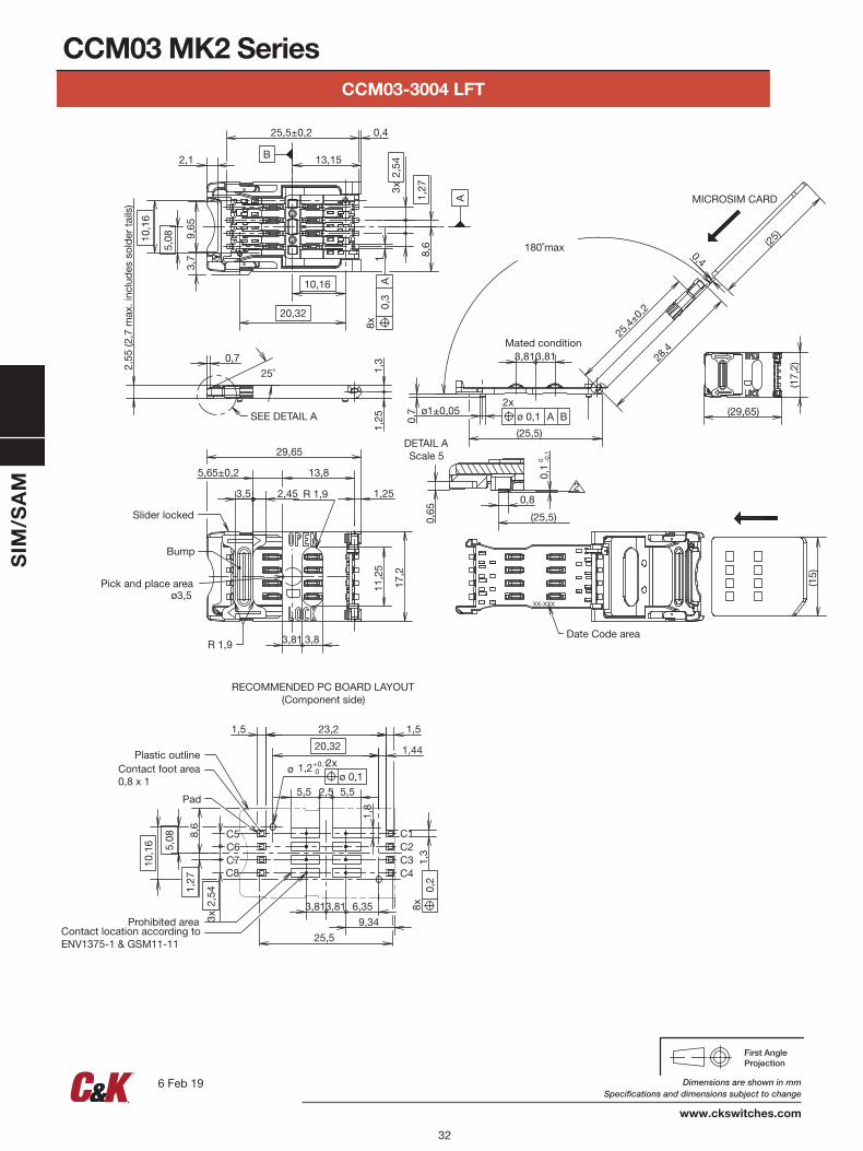
CCM03-3004 LFT
CCM03 MK2 SeriesS
IM/S
AM
MICROSIM CARD
R 1,9
1,3
1,25
2,55
(2,7
max
. inc
lud
es s
old
er t
ails
)
11,2
5
17,2
3,81 3,8
3,5 2,45 1,25
5,65±0,2 13,8
29,65
(17,
2)
(29,65)
00,
1 -
0,1
0,7
25˚
0,8
(25,5)
3x2,
54
R 1,9
0,65
0,425,5±0,2
13,152,1
9,65
3,7 1
0,3
A
1,27
8,6
10,16
20,32
5,0810
,16
3,813,81
25,4
±0,2
0,4180˚max
(25,5)
(25)
28,4
(15)
�ø1±0,05 ø 0,1 A B0,7
XX-XXX
SEE DETAIL A
Date Code area
Mated condition
8x
2x
Pick and place area ø3,5
Slider locked
Bump
DETAIL AScale 5
A
B
2
1,27
8,6
23,2
25,5
2,5 5,55,5
3,813,81
1,8
1,5 1,5
9,34
6,35
20,32
10,1
6 5,08
+0,1ø 1,2 0ø 0,1
1,44
3x2,
54
1,3
0,2
Contact location according to ENV1375-1 & GSM11-11
Contact foot area 0,8 x 1
RECOMMENDED PC BOARD LAYOUT(Component side)
Prohibited area
8x
C5
Plastic outline
Pad
C6C7
C1C2C3
2x
C8 C4
6 Feb 19
33
Dimensions are shown in mm Specifications and dimensions subject to change
www.ckwitches.com
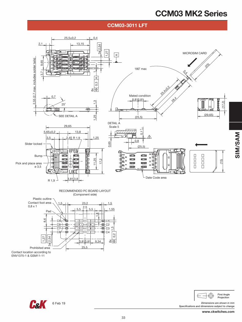
CCM03-3011 LFT
CCM03 MK2 Series
SIM
/SA
M
MICROSIM CARD
R 1,9
1
1,3
1,25
2,55
(2,7
max
. inc
lud
es s
old
er t
ails
)
11,2
5
17,2
3,81 3,8
3,5 2,45 1,25
5,65±0,2 13,8
29,65
(17,
2)
(29,65)
00,
1 -
0,1
0,7
25˚
0,8
(25,5)
3x2,
54
13,15
0,425,5±0,2
2,19,
653,
7
0,65
R 1,9
10,
3A
1,27
3,813,81
25,4
±0,2
0,4180˚ max
(25,5)
(25)
28,4
(15)
XX-XXX
SEE DETAIL A
Date Code area
Mated condition8x
Pick and place area ø 3,5
Slider locked
Bump
DETAIL AScale 5
A
2
1,27
8,6
23,2
25,5
2,55,55,5
3,813,81
1,8
1,5 1,5
9,34
1,55
3x2,
54
1,3
0,2
Contact location according to ENV1375-1 & GSM11-11
C5
Contact foot area 0,8 x 1
RECOMMENDED PC BOARD LAYOUT(Component side)
Prohibited area
C6C7
C1C2C3
C8 C4
8x
Plastic outline
Pad
6 Feb 19
34
Dimensions are shown in mm Specifications and dimensions subject to change
www.ckwitches.com
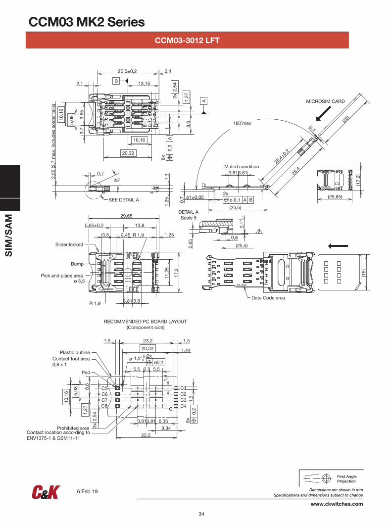
CCM03-3012 LFT
CCM03 MK2 SeriesS
IM/S
AM
MICROSIM CARD
R 1,9
1,3
1,25
2,55
(2,7
max
. inc
lud
es s
old
er t
ails
)
11,2
5
17,2
3,81 3,8
3,5 2,45 1,25
5,65±0,2 13,8
29,65
(17,
2)
(29,65)
00,
1 -
0,1
0,7
25˚
0,8
(25,5)
3x2,
54
R 1,9
0,65
0,425,5±0,2
13,152,19,
65
10,
3A
1,27
8,6
10,16
20,32
5,0810
,16
3,7
3,813,81
25,4
±0,2
0,4180˚max
(25,5)
(25)
28,4
(15)
�ø1±0,05 ø 0,1 A B0,7
XX-XXX
SEE DETAIL A
Date Code area
Mated condition8x
2x
Pick and place area �ø 3,5
Slider locked
Bump
DETAIL AScale 5
A
B
2
1,27
8,6
23,2
25,5
2,5 5,55,5
3,813,81
1,8
1,5 1,5
9,34
6,35
20,32
10,1
6 5,08
+0,1ø 1,2 0�ø0,1
1,44
3x2,
54
1,3
0,2
Contact location according to ENV1375-1 & GSM11-11
Contact foot area 0,8 x 1
RECOMMENDED PC BOARD LAYOUT(Component side)
Prohibited area
8x
C5
Plastic outline
Pad
C6C7
C1C2C3
2x
C8 C4
6 Feb 19
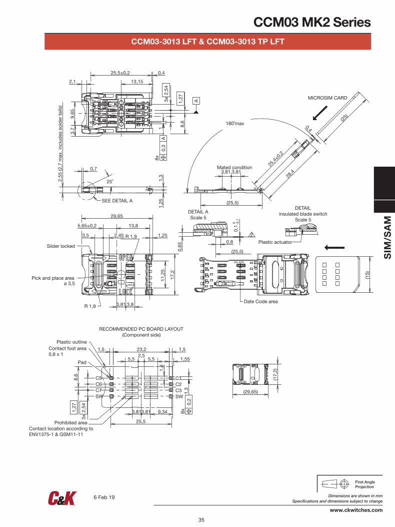
35
Dimensions are shown in mm Specifications and dimensions subject to change
www.ckwitches.com
CCM03-3013 LFT & CCM03-3013 TP LFT
CCM03 MK2 Series
SIM
/SA
M
MICROSIM CARD
R 1,9
1,3
1,25
2,55
(2,7
max
. inc
lud
es s
old
er t
ails
)
11,2
5
17,2
3,81 3,8
3,5 2,45 1,25
5,65±0,2 13,8
29,65
(17,
2)
(29,65)
0,7
25˚
13,152,1
9,65
0,65
R 1,9
10,
3A
00,
1-0
,10,8
25,5±0,2 0,4
(25,5)
3x2,
54
8,6
1,27
3,7
3,81 3,8125
,4±0,
2
0,4180˚max
(25)
28,4
(15)
(25,5)
XX-XXX
SEE DETAIL A
Date Code area
Mated condition
8x
DETAILinsulated blade switch
Scale 5
Pick and place area ø 3,5
Slider locked
DETAIL AScale 5
Plastic actuator
A
2
1,27
8,6
23,2
25,5
2,55,55,5
3,813,81
1,8
1,5 1,5
9,34
1,55
3x2,
54
1,3
0,2
Contact location according to ENV1375-1 & GSM11-11
C5
Contact foot area 0,8 x 1
RECOMMENDED PC BOARD LAYOUT(Component side)
Prohibited area
C6C7
C1C2C3
SW SW
8x
Plastic outline
Pad
6 Feb 19
36
Dimensions are shown in mm Specifications and dimensions subject to change
www.ckswitches.com
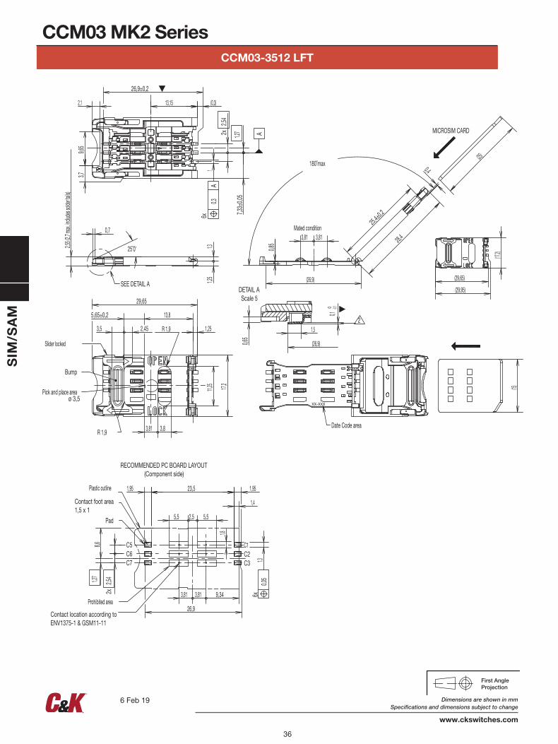
CCM03-3512 LFT
SIM
/SA
M
CCM03 MK2 Series
MICROSIM CARD
R 1,9
1,31,2
5
2,55 (2
,7 max.
includ
es sol
der tai
ls)
17,2
3,81 3,8
3,5 2,45 1,25
5,65±0,2 13,8
29,65
(17,2)
(29,65)
0,7
25˚0'
1,27
26,9±0,2
(26,9)
1,5 0
0,1-0,1
0,65
R 1,9
9,65
2x2,5
4
(0,3)13,152,1
10,3
A
(29,95)
11,25
7,33±
0,05
3,7
3,81 3,81
25,4±0,2
0,4180˚max
(25)
28,4
(15)
(26,9)0,8
5
XX-XXX
SEE DETAIL A
RECOMMENDED PC BOARD LAYOUT(Component side)
Date Code area
Mated condition
6x
Pick and place area ø 3,5
Slider locked
Bump
DETAIL AScale 5
A
2
1,27
8,6
23,5
26,9
2,5 5,55,5
3,81 3,81
1,8
1,95 1,95
9,34
1,30,0
5
2x2,5
4
1,4
Contact location according to ENV1375-1 & GSM11-11
C5
Contact foot area 1,5 x 1
C6C7
6x
Plastic outline
Pad
Prohibited area
C1C2C3
6 Feb 19
37
Dimensions are shown in mm Specifications and dimensions subject to change
www.ckswitches.com
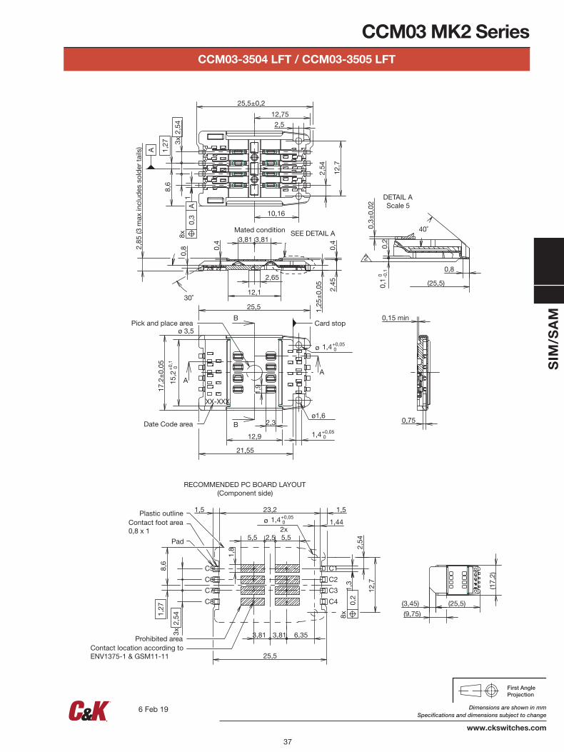
CCM03-3504 LFT / CCM03-3505 LFT
CCM03 MK2 Series
SIM
/SA
M
2
(3,45)
21,55
+0,05ø 1,4 0
0,15 min
2,45
ø1,6
+0,051,4 0
0,8
30˚
0,8
1,25
±0,
05
0,2
2,65
12,1
+0,
115
,2 0
17,2
±0,
05
AA
B
B
1,9
2,3
40˚
(25,5)
0,75
25,5±0,2
12,7
2,5
3x2,
541
0,3
A
10,16
3,813,81
0,3±
0,02
0,4
2,54
00,
1-0
,1
8,6
1,27
12,75
25,5
(25,5)
(17,
2)
(9,75)
12,9
0,4
2,85
(3 m
ax in
clud
es s
old
er t
ails
)
Date Code area
Card stop
Mated condition
XX-XXX
Pick and place area ø 3,5
SEE DETAIL A 8x
RECOMMENDED PC BOARD LAYOUT(Component side)
DETAIL AScale 5
A
6,35
2,542,55,5 5,5
1,8
25,5
3,81 3,81
+0,05ø 1,4 0
2x
8,6
1,523,21,5
1,44
3x2,
541,27
12,7
1,3
0,2
Contact location according to ENV1375-1 & GSM11-11
C1C5
Contact foot area 0,8 x 1
C2
C3
C4
C6
C7
C8
8x
Plastic outline
Pad
Prohibited area
6 Feb 19