Embed Size (px)
Citation preview
CCS811Ultra-Low Power Digital Gas Sensor for Monitoring Indoor Air Quality
The CCS811 is an ultra-low power digital gas sensor solution which integrates a metal oxide (MOX) gas sensor to detect a wide range of Volatile Organic Compounds (VOCs) for indoor air quality monitoring with a microcontroller unit (MCU), which includes an Analog-to-Digital converter (ADC), and an I²C interface.
CCS811 is based on ams unique micro-hotplate technology which enables a highly reliable solution for gas sensors, very fast cycle times and a significant reduction in average power consumption.
The integrated MCU manages the sensor driver modes and measurements. The I²C digital interface significantly simplifies the hardware and software design, enabling a faster time to market.
CCS811 supports intelligent algorithms to process raw sensor measurements to output equivalent total VOC (eTVOC) and equivalent CO2 (eCO2) values, where the main cause of VOCs is from humans.
CCS811 supports multiple measurement modes that have been optimized for low-power consumption during an active sensor measurement and idle mode extending battery life in portable applications.
CCS811 is available in a 10 lead 2.7mm x 4.0mm x 1.1mm, 0.6mm pitch LGA package.
Ordering Information and Content Guide appear at end of datasheet.
General Description
ams Datasheet Page 1[v1-06] 2019-Feb-07 Document Feedback
CCS811 − General Description
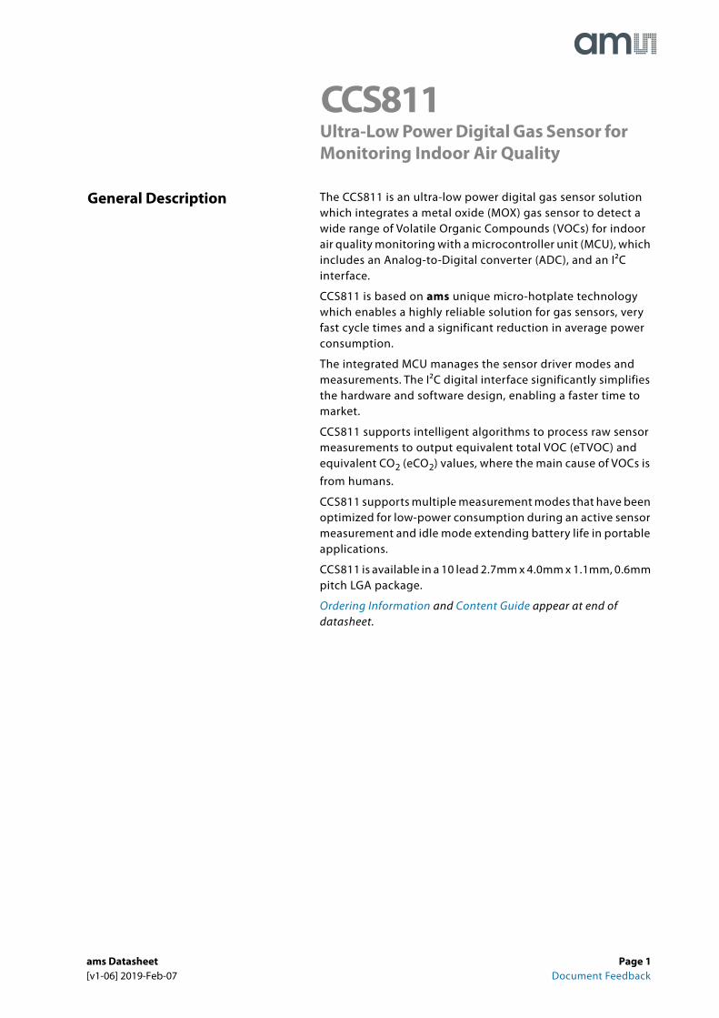
Key Benefits & FeaturesThe benefits and features of CCS811, Ultra-Low Power Digital Gas Sensor for Monitoring Indoor Air Quality are listed below:
Figure 1:Added Value of Using CCS811 Sensor
ApplicationsThis device can be mainly used for indoor air quality monitoring in:
• Smart phones
• Air cleaners and purifiers
• Smart thermostats
• Home controllers
• Smart accessories and IoT devices
Benefits Features
• Manages the sensor drive modes and measurements while detecting VOCs
• Integrated MCU
• Provides eCO2 level or eTVOC indication with no host intervention
• On-board processing
• Simplifies the hardware and software integration• Standard (100kbit/s) and fast (400kbit/s)
I²C interface
• Extend battery life in portable applications • Optimised low-power modes
• Suitable for small form-factor designs • 2.7mm x 4.0mm x 1.1mm LGA package
• Saves up to 60% in PCB footprint • Low component count
• Designed for high volume and reliability (>5years lifetime)
• Proven technology platform
Page 2 ams Datasheet Document Feedback [v1-06] 2019-Feb-07
CCS811 − General Description
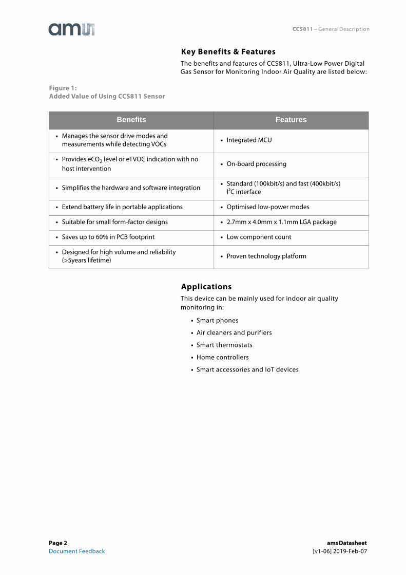
Block DiagramThe functional blocks of this device are shown below:
Figure 2:CCS811 Block Diagram
MOXGas Sensor
S+
H-
H+
nINT
nRESET
ADDR
SDA
SCL
V DD
GND
nWAK
E S-
7
2
3
4EP
18 9 10
5
6
MCU(With Integrated ADC)
PWM
Sens
e
Pins 4 and 5 must be connected together
ams Datasheet Page 3[v1-06] 2019-Feb-07 Document Feedback
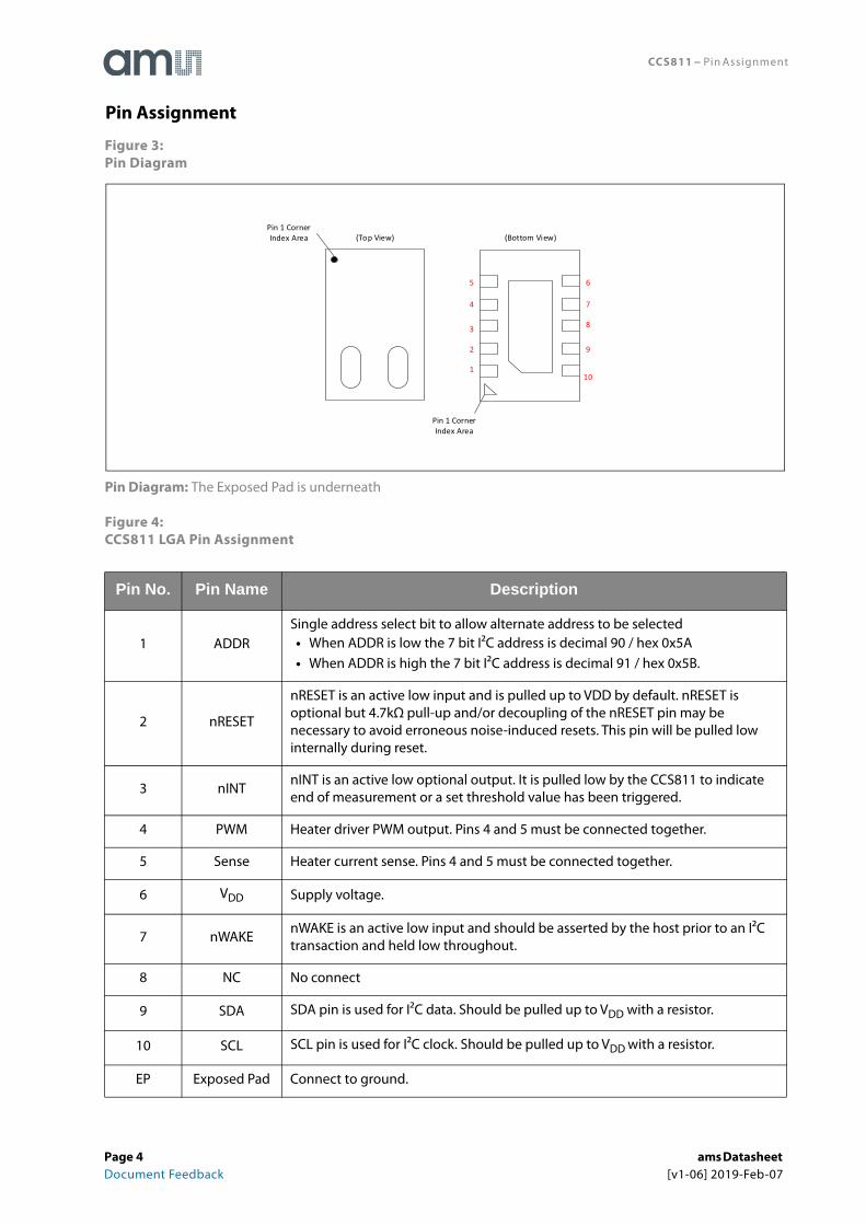
CCS811 − Pin Assignment
Figure 3:Pin Diagram
Pin Diagram: The Exposed Pad is underneath
Figure 4:CCS811 LGA Pin Assignment
Pin No. Pin Name Description
1 ADDRSingle address select bit to allow alternate address to be selected• When ADDR is low the 7 bit I²C address is decimal 90 / hex 0x5A• When ADDR is high the 7 bit I²C address is decimal 91 / hex 0x5B.
2 nRESET
nRESET is an active low input and is pulled up to VDD by default. nRESET is optional but 4.7kΩ pull-up and/or decoupling of the nRESET pin may be necessary to avoid erroneous noise-induced resets. This pin will be pulled low internally during reset.
3 nINTnINT is an active low optional output. It is pulled low by the CCS811 to indicate end of measurement or a set threshold value has been triggered.
4 PWM Heater driver PWM output. Pins 4 and 5 must be connected together.
5 Sense Heater current sense. Pins 4 and 5 must be connected together.
6 VDD Supply voltage.
7 nWAKEnWAKE is an active low input and should be asserted by the host prior to an I²C transaction and held low throughout.
8 NC No connect
9 SDA SDA pin is used for I²C data. Should be pulled up to VDD with a resistor.
10 SCL SCL pin is used for I²C clock. Should be pulled up to VDD with a resistor.
EP Exposed Pad Connect to ground.
Pin Assignment
Pin 1 Corner Index Area (Top View)
Pin 1 Corner Index Area
(Bottom View)
1
5
10
6
7
8
9
4
3
2
Page 4 ams Datasheet Document Feedback [v1-06] 2019-Feb-07
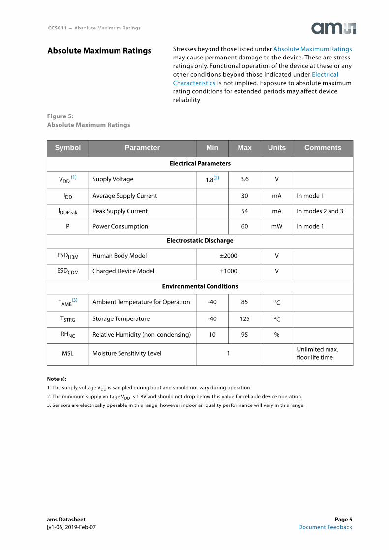
CCS811 − Absolute Maximum Ratings
Stresses beyond those listed under Absolute Maximum Ratings may cause permanent damage to the device. These are stress ratings only. Functional operation of the device at these or any other conditions beyond those indicated under Electrical Characteristics is not implied. Exposure to absolute maximum rating conditions for extended periods may affect device reliability
Figure 5:Absolute Maximum Ratings
Note(s):
1. The supply voltage VDD is sampled during boot and should not vary during operation.
2. The minimum supply voltage VDD is 1.8V and should not drop below this value for reliable device operation.
3. Sensors are electrically operable in this range, however indoor air quality performance will vary in this range.
Symbol Parameter Min Max Units Comments
Electrical Parameters
VDD (1) Supply Voltage 1.8(2) 3.6 V
IDD Average Supply Current 30 mA In mode 1
IDDPeak Peak Supply Current 54 mA In modes 2 and 3
P Power Consumption 60 mW In mode 1
Electrostatic Discharge
ESDHBM Human Body Model ±2000 V
ESDCDM Charged Device Model ±1000 V
Environmental Conditions
TAMB(3) Ambient Temperature for Operation -40 85 oC
TSTRG Storage Temperature -40 125 oC
RHNC Relative Humidity (non-condensing) 10 95 %
MSL Moisture Sensitivity Level 1Unlimited max. floor life time
Absolute Maximum Ratings
ams Datasheet Page 5[v1-06] 2019-Feb-07 Document Feedback
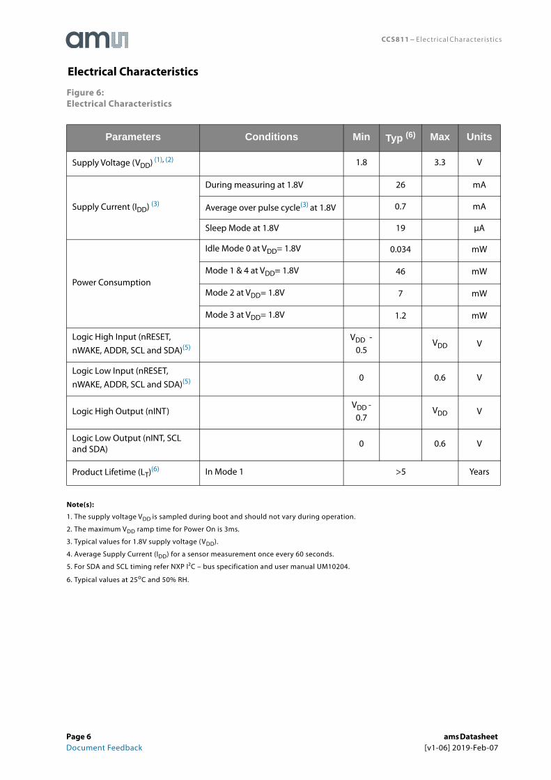
CCS811 − Electrical Characteristics
Figure 6:Electrical Characteristics
Note(s):
1. The supply voltage VDD is sampled during boot and should not vary during operation.
2. The maximum VDD ramp time for Power On is 3ms.
3. Typical values for 1.8V supply voltage (VDD).
4. Average Supply Current (IDD) for a sensor measurement once every 60 seconds.
5. For SDA and SCL timing refer NXP I²C – bus specification and user manual UM10204.
6. Typical values at 25oC and 50% RH.
Parameters Conditions Min Typ (6) Max Units
Supply Voltage (VDD) (1), (2) 1.8 3.3 V
Supply Current (IDD) (3)
During measuring at 1.8V 26 mA
Average over pulse cycle(3) at 1.8V 0.7 mA
Sleep Mode at 1.8V 19 μA
Power Consumption
Idle Mode 0 at VDD= 1.8V 0.034 mW
Mode 1 & 4 at VDD= 1.8V 46 mW
Mode 2 at VDD= 1.8V 7 mW
Mode 3 at VDD= 1.8V 1.2 mW
Logic High Input (nRESET, nWAKE, ADDR, SCL and SDA)(5)
VDD - 0.5
VDD V
Logic Low Input (nRESET, nWAKE, ADDR, SCL and SDA)(5) 0 0.6 V
Logic High Output (nINT)VDD -
0.7VDD V
Logic Low Output (nINT, SCL and SDA)
0 0.6 V
Product Lifetime (LT)(6) In Mode 1 >5 Years
Electrical Characteristics
Page 6 ams Datasheet Document Feedback [v1-06] 2019-Feb-07
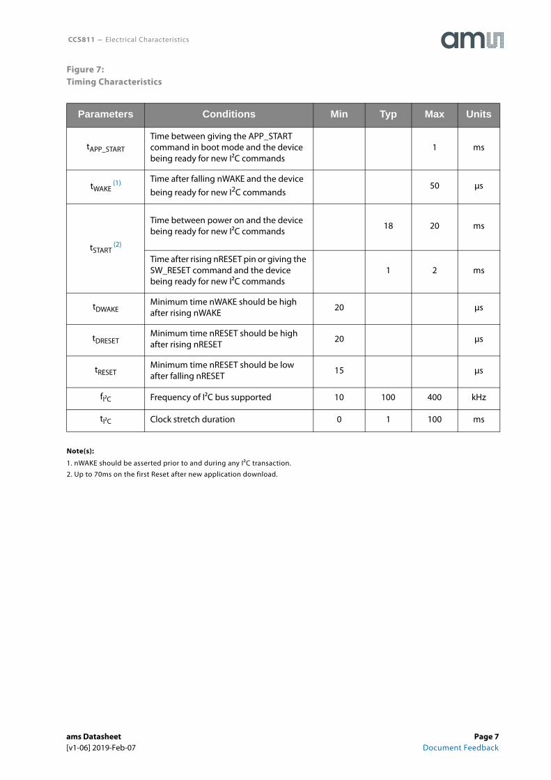
CCS811 − Electrical Characteristics
Figure 7:Timing Characteristics
Note(s):
1. nWAKE should be asserted prior to and during any I²C transaction.
2. Up to 70ms on the first Reset after new application download.
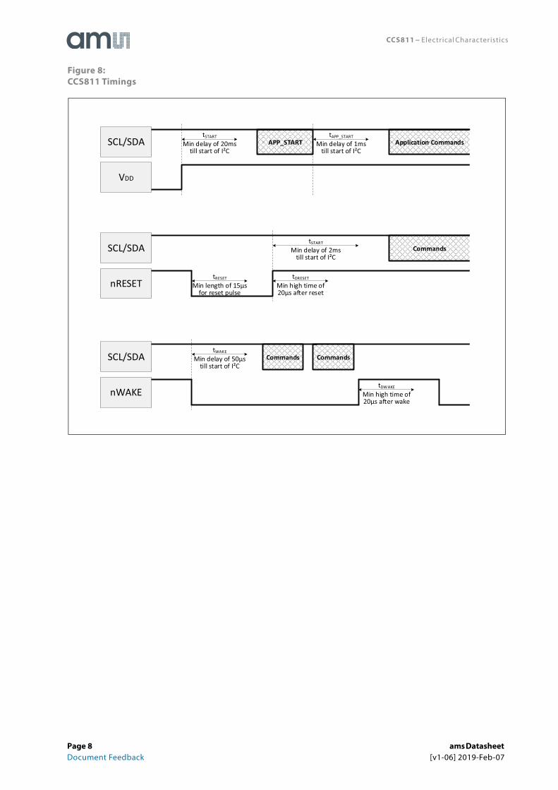
Parameters Conditions Min Typ Max Units
tAPP_START
Time between giving the APP_START command in boot mode and the device being ready for new I²C commands
1 ms
tWAKE (1) Time after falling nWAKE and the device
being ready for new I2C commands50 μs
tSTART (2)
Time between power on and the device being ready for new I²C commands
18 20 ms
Time after rising nRESET pin or giving the SW_RESET command and the device being ready for new I²C commands
1 2 ms
tDWAKEMinimum time nWAKE should be high after rising nWAKE
20 μs
tDRESETMinimum time nRESET should be high after rising nRESET
20 μs
tRESETMinimum time nRESET should be low after falling nRESET
15 μs
fI²C Frequency of I²C bus supported 10 100 400 kHz
tI²C Clock stretch duration 0 1 100 ms
ams Datasheet Page 7[v1-06] 2019-Feb-07 Document Feedback
CCS811 − Electrical Characteristics
Figure 8:CCS811 Timings
Min delay of 20ms till start of I²C
tSTARTAPP_START Min delay of 1ms
till start of I²C
tAPP_START
Min high time of 20μs after reset
tDRESET
nRESET
SCL/SDA
VDD
Application Commands
Min length of 15μs for reset pulse
tRESET
Min delay of 2ms till start of I²C
tSTARTCommands
nWAKE
SCL/SDA Commands
SCL/SDA
Min delay of 50μs till start of I²C
tWAKECommands
tDWAKE
Min high time of 20μs after wake
Page 8 ams Datasheet Document Feedback [v1-06] 2019-Feb-07
CCS811 − Detailed Description
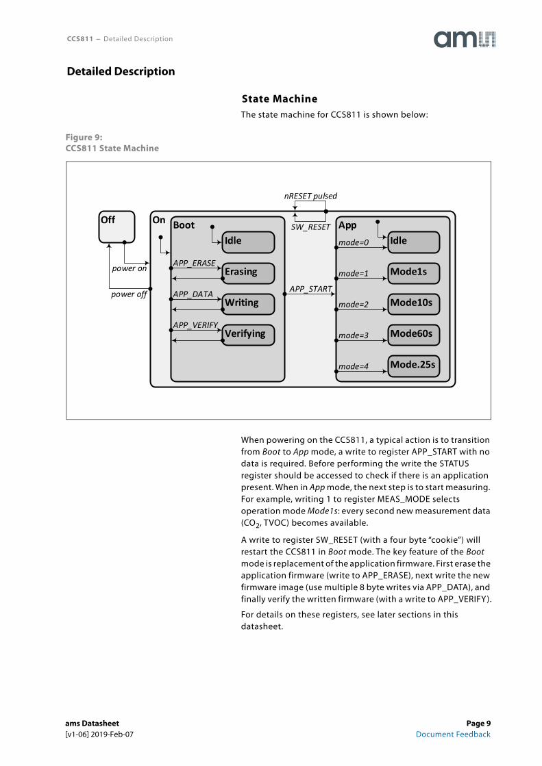
State MachineThe state machine for CCS811 is shown below:
Figure 9:CCS811 State Machine
When powering on the CCS811, a typical action is to transition from Boot to App mode, a write to register APP_START with no data is required. Before performing the write the STATUS register should be accessed to check if there is an application present. When in App mode, the next step is to start measuring. For example, writing 1 to register MEAS_MODE selects operation mode Mode1s: every second new measurement data (CO2, TVOC) becomes available.
A write to register SW_RESET (with a four byte “cookie”) will restart the CCS811 in Boot mode. The key feature of the Boot mode is replacement of the application firmware. First erase the application firmware (write to APP_ERASE), next write the new firmware image (use multiple 8 byte writes via APP_DATA), and finally verify the written firmware (with a write to APP_VERIFY).
For details on these registers, see later sections in this datasheet.
Detailed Description
Off On Boot AppSW_RESET
nRESET pulsed
power on
power off APP_START
ErasingAPP_ERASE
WritingAPP_DATA
VerifyingAPP_VERIFY
Idle
Mode1s
Mode10s
Mode60s
mode=0
mode=1
mode=2
mode=3
Idle
Mode.25smode=4
ams Datasheet Page 9[v1-06] 2019-Feb-07 Document Feedback
CCS811 − Detailed Description
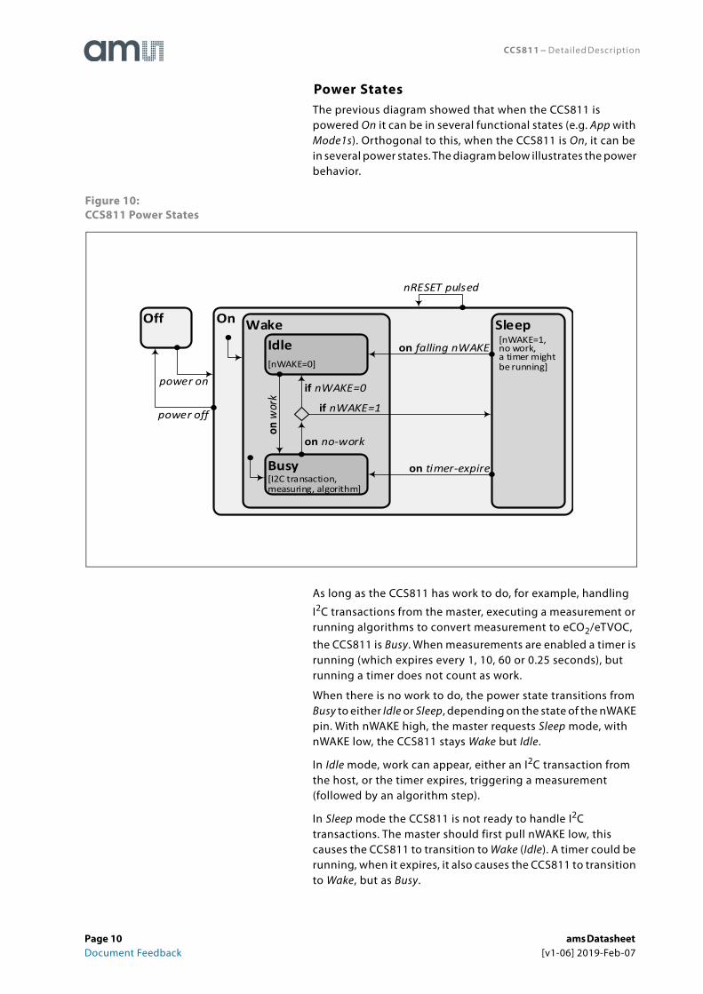
Power StatesThe previous diagram showed that when the CCS811 is powered On it can be in several functional states (e.g. App with Mode1s). Orthogonal to this, when the CCS811 is On, it can be in several power states. The diagram below illustrates the power behavior.
Figure 10:CCS811 Power States
As long as the CCS811 has work to do, for example, handling
I2C transactions from the master, executing a measurement or running algorithms to convert measurement to eCO2/eTVOC, the CCS811 is Busy. When measurements are enabled a timer is running (which expires every 1, 10, 60 or 0.25 seconds), but running a timer does not count as work.
When there is no work to do, the power state transitions from Busy to either Idle or Sleep, depending on the state of the nWAKE pin. With nWAKE high, the master requests Sleep mode, with nWAKE low, the CCS811 stays Wake but Idle.
In Idle mode, work can appear, either an I2C transaction from the host, or the timer expires, triggering a measurement (followed by an algorithm step).
In Sleep mode the CCS811 is not ready to handle I2C transactions. The master should first pull nWAKE low, this causes the CCS811 to transition to Wake (Idle). A timer could be running, when it expires, it also causes the CCS811 to transition to Wake, but as Busy.
On WakeIdle
Busy
on no-work
if nWAKE=0
if nWAKE=1
Sleepon falling nWAKE
on timer-expire
on w
ork
[I2C transaction, measuring, algorithm]
[nWAKE=0]
Off
power on
power off
[nWAKE=1, no work, a timer might be running]
nRESET pulsed
Page 10 ams Datasheet Document Feedback [v1-06] 2019-Feb-07
CCS811 − Detailed Description
Note that a hardware reset (via the nRESET) pin can be triggered irrespective of the power state (assuming On), for a SW_RESET, the CCS811 needs to be Wake.
So, tying nWAKE to ground is the simplest hardware configuration – CCS811 will always be Wake and ready to communicate but consumes more power. If power consumption is a concern, the master should set nWAKE low
before I2C communication and high afterwards. If measurements are enabled, the CCS811 will use a timer to wake up itself periodically to execute a measurement.
Modes of OperationThe CCS811 has 5 modes of operation as follows
• Mode 0: Idle, low current mode
• Mode 1: Constant power mode, IAQ measurement every second
• Mode 2: Pulse heating mode IAQ measurement every 10 seconds
• Mode 3: Low power pulse heating mode IAQ measurement every 60 seconds
• Mode 4: Constant power mode, sensor measurement every 250ms
In Modes 1, 2, 3, the equivalent CO2 concentration (ppm) and eTVOC concentration (ppb) are calculated for every sample.
• Mode 1 reacts fastest to gas presence, but has a higher operating current
• Mode 3 reacts more slowly to gas presence but has the lowest average operating current.
When a sensor operating mode is changed to a new mode with a lower sample rate (e.g. from Mode 1 to Mode 3), it should be placed in Mode 0 (Idle) for at least 10 minutes before enabling the new mode. When a sensor operating mode is changed to a new mode with a higher sample rate (e.g. from Mode 3 to Mode 1), there is no requirement to wait before enabling the new mode.
Mode 4 is intended for systems where an external host system wants to run an algorithm with raw data and this mode provides new sample data every 250ms. Mode 4 is also recommended for end-of-line production test to save test time. For additional information please refer to application note ams AN000373: CCS811 Factory test procedure.
Note(s): Mode timings are subject to typical 2% tolerance due to accuracy of internal clock
ams Datasheet Page 11[v1-06] 2019-Feb-07 Document Feedback
CCS811 − Detailed Description
Early-Life (Burn-In)CCS811 performance in terms of resistance levels and sensitivities will change during early life. The change in resistance is greatest over the first 48 hours of operation. CCS811 controls the burn-in period allowing eCO2 and eTVOC readings to be used from first power-on after 60 minutes of operation in modes 1-3.
Conditioning Period (Run-In)After early-life (Burn-In) the conditioning or run-in period is the time required to achieve good sensor stability before measuring VOCs after long idle period.
After writing to MEAS_MODE to configure the sensor in mode 1-4, run CCS811 for 20 minutes, before accurate readings are generated.
The conditioning period must also be observed before writing to the BASELINE register.
eCO2
The equivalent CO2 (eCO2) output range for CCS811 is from 400ppm up to 29206ppm.
eTVOCThe equivalent Total Volatile Organic Compound (eTVOC) output range for CCS811 is from 0ppb up to 32768ppb.
Temperature and Humidity CompensationIf an external sensor is available this information can be written to CCS811 so that they will be used to compensate gas readings due to temperature and humidity changes. When ENV_DATA has been written, the next eCO2 and eTVOC readings (in ALG_RESULT_DATA) may not yet use the latest ENV_DATA. All subsequent reading will use the ALG_RESULT_DATA. Refer to the ENV_DATA (Environment Data) Register (0x05).
Interrupt and Interrupt on ThresholdAt the end of each measurement cycle (250ms, 1s, 10s, 60s) a flag is set and optionally interrupt (nINT) pin asserted. Refer to the MEAS_MODE (Measurement and Conditions) Register (0x01). The user can choose to only assert nINT if the eCO2 value changes into a different range set by register values. Refer to the THRESHOLDS Register (0x10).
Page 12 ams Datasheet Document Feedback [v1-06] 2019-Feb-07
CCS811 − Detailed Description
Automatic Baseline CorrectionThe resistance RS of the sensitive layer is the output of the sensor. However, metal oxide sensors do not give absolute readings. The resistance RS varies from sensor to sensor (manufacturing variation), from use-case to use-case, and over time. To mitigate this problem, the output of the sensor is normalized: RS is divided by RA. The value of RA is known as the baseline. RA cannot be determined by a one-time calibration; it is maintained on-the-fly in software. This process is known as baseline correction. The air quality is expected to vary in a typical environment so the minimum time over which a baseline correction is applied is 24 hours. Automatic baseline correction is enabled after initial device operation.
Manual Baseline CorrectionThere is a mechanism within CCS811 to manually save and restore a previously saved baseline value using the BASELINE register.
For additional information on manual baseline control please refer to application note ams AN000370: CCS811 Clean Air Baseline Save and Restore.
ams Datasheet Page 13[v1-06] 2019-Feb-07 Document Feedback
CCS811 − Application Information
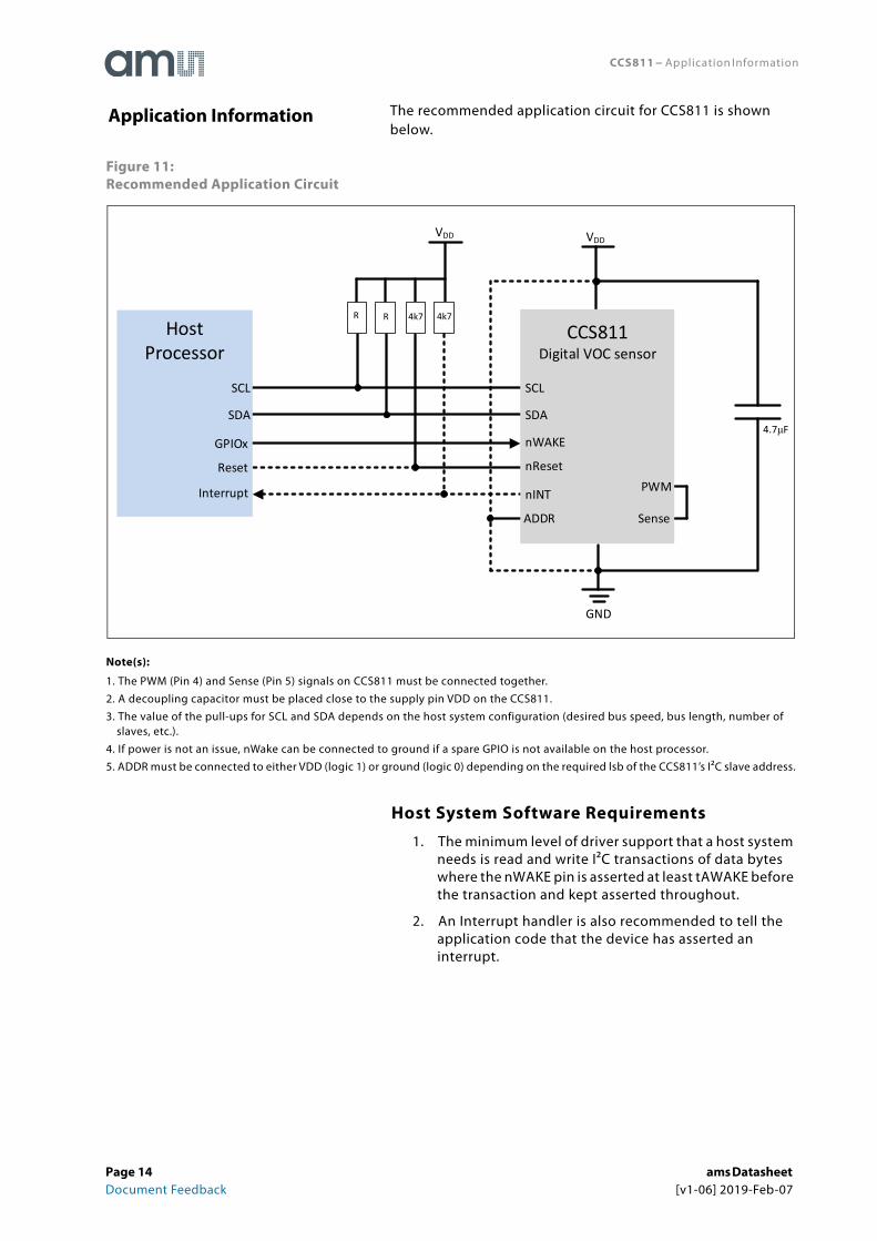
The recommended application circuit for CCS811 is shown below.
Figure 11:Recommended Application Circuit
Note(s):
1. The PWM (Pin 4) and Sense (Pin 5) signals on CCS811 must be connected together.
2. A decoupling capacitor must be placed close to the supply pin VDD on the CCS811.
3. The value of the pull-ups for SCL and SDA depends on the host system configuration (desired bus speed, bus length, number of slaves, etc.).
4. If power is not an issue, nWake can be connected to ground if a spare GPIO is not available on the host processor.
5. ADDR must be connected to either VDD (logic 1) or ground (logic 0) depending on the required lsb of the CCS811’s I²C slave address.
Host System Software Requirements
1. The minimum level of driver support that a host system needs is read and write I²C transactions of data bytes where the nWAKE pin is asserted at least tAWAKE before the transaction and kept asserted throughout.
2. An Interrupt handler is also recommended to tell the application code that the device has asserted an interrupt.
Application Information
Host Processor
VDD
R
SDA
SCL
VDD
GND
CCS811Digital VOC sensor
4k7
4.7μFGPIOx
SDA
ADDR
SCL
nWAKE
PWM
Sense
nResetReset
R
nINTInterrupt
4k7
Page 14 ams Datasheet Document Feedback [v1-06] 2019-Feb-07
CCS811 − Application Information
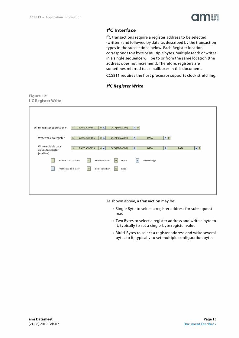
I²C InterfaceI²C transactions require a register address to be selected (written) and followed by data, as described by the transaction types in the subsections below. Each Register location corresponds to a byte or multiple bytes. Multiple reads or writes in a single sequence will be to or from the same location (the address does not increment). Therefore, registers are sometimes referred to as mailboxes in this document.
CCS811 requires the host processor supports clock stretching.
I²C Register Write
Figure 12:I²C Register Write
As shown above, a transaction may be:
• Single Byte to select a register address for subsequent read
• Two Bytes to select a register address and write a byte to it, typically to set a single-byte register value
• Multi-Bytes to select a register address and write several bytes to it, typically to set multiple configuration bytes
SLAVE ADDRESSS W A DATA(REG ADDR)
DATA
A P
SLAVE ADDRESSS W A DATA(REG ADDR) A
PSLAVE ADDRESSS W A DATA(REG ADDR) A
P
A
A
ADATA
DATA
Write, register address only
Write value to register
Write multiple data values to register (mailbox)
From master to slave
From slave to master
S Start condition
P STOP condition
W
R
Write
Read
A Acknowledge
ams Datasheet Page 15[v1-06] 2019-Feb-07 Document Feedback
CCS811 − Application Information
I²C Register Read
Figure 13:I²C Register Read
• Since no register address can be supplied during an I²C read, an I²C write needs to be prepended to select the required register first.
• The write and read operations can optionally be combined into a single transaction using a repeated start condition, as shown in the second example above.
• Select and repeatedly read multiple data values from register, if the three reads are from the same register (mailbox), or from three subsequent registers (mailboxes).
SLAVE ADDRESSS W A DATA(REG ADDR) A P
SLAVE ADDRESSS R A PNDATA
Select and read register value
Select and repeatedly read multiple data values from register
(select register address)
(read register value)
Select and read register value, as single transaction
SLAVE ADDRESSS W A DATA(REG ADDR) A S SLAVE ADDRESS R A PNDATA
SLAVE ADDRESSS W A DATA(REG ADDR) A P (select register address)
(select register address) (read register value)
SLAVE ADDRESSS R A PADATA NDATA (read register multiple data)
SLAVE ADDRESSS R A PADATA NDATA (read register multiple data)
SLAVE ADDRESSS R A PADATA NDATA (read register multiple data)
From master to slave
From slave to master
S Start condition
P STOP condition
W
R
Write
Read
A
N
Acknowledge
Not acknowledge
Page 16 ams Datasheet Document Feedback [v1-06] 2019-Feb-07
CCS811 − Application Register Overview
All I²C transactions must use the (7 bits) slave address 0x5A or 0x5B depending on status of ADDR pin when writing to and reading from the CCS811. Figure 14 shows the register map for CCS811. Figure 25 shows the bootloader register map.
Figure 14:CCS811 Application Register Map
Note(s):
1. The number of bytes read from a register must not exceed the size in this table.
2. For more information on CCS811 programming requirements please refer to ams application note AN000369.
Address Register R/W Size Description
0x00 STATUS R 1 byte Status register
0x01 MEAS_MODE R/W 1 byte Measurement mode and conditions register
0x02 ALG_RESULT_DATA Rup to
8 bytes
Algorithm result. The most significant 2 bytes contain a ppm estimate of the equivalent CO2 (eCO2) level, and the next two bytes contain a ppb estimate of the total VOC level.
0x03 RAW_DATA R 2 bytesRaw ADC data values for resistance and current source used.
0x05 ENV_DATA W 4 bytesTemperature and humidity data can be written to enable compensation
0x10 THRESHOLDS W 4 bytesThresholds for operation when interrupts are only generated when eCO2 ppm crosses a threshold
0x11 BASELINE R/W 2 bytesThe encoded current baseline value can be read. A previously saved encoded baseline can be written.
0x20 HW_ID R 1 byte Hardware ID. The value is 0x81
0x21 HW Version R 1 byte Hardware Version. The value is 0x1X
0x23 FW_Boot_Version R 2 bytesFirmware Boot Version. The first 2 bytes contain the firmware version number for the boot code.
0x24 FW_App_Version R 2 bytesFirmware Application Version. The first 2 bytes contain the firmware version number for the application code
0xA0 Internal_State R 1 byte Internal Status register
0xE0 ERROR_ID R 1 byteError ID. When the status register reports an error its source is located in this register
0xFF SW_RESET W 4 bytesIf the correct 4 bytes (0x11 0xE5 0x72 0x8A) are written to this register in a single sequence the device will reset and return to BOOT mode.
Application Register Overview
ams Datasheet Page 17[v1-06] 2019-Feb-07 Document Feedback
CCS811 − Application Register Overview
STATUS Register (0x00)Single byte read only register which indicates if a device is active, if new data is available or if an error occurred.
Figure 15:Status Register
7 6 5 4 3 2 1 0
FW_MODE APP_ERASE APP_VERIFY APP_VALID DATA_READY - ERROR
Bit(s) Field Description
7 FW_MODE0: Firmware is in boot mode, this allows new firmware to be loaded1: Firmware is in application mode. CCS811 is ready to take ADC measurements
6 APP_ERASE
Boot Mode only.0: No erase completed1: Application erase operation completed successfully (flag is cleared by APP_DATA and also by APP_START, SW_RESET, nRESET and APP_VERIFY) After issuing the ERASE command the application software must wait 500ms before issuing any transactions to the CCS811 over the I2C interface.
5 APP_VERIFY
Boot Mode only. 0: No verify completed1: Application verify operation completed successfully (flag is cleared by APP_START, SW_RESET and nRESET)After issuing a VERIFY command the application software must wait 70ms before issuing any transactions to CCS811 over the I²C interface
4 APP_VALID0: No application firmware loaded1: Valid application firmware loaded
3 DATA_READY0: No new data samples are ready1: A new data sample is ready in ALG_RESULT_DATA, this bit is cleared when ALG_RESULT_DATA is read on the I²C interface
2:1 - Reserved
0 ERROR
This bit is cleared by reading ERROR_ID (it is not sufficient to read the ERROR field of ALG_RESULT_DATA and STATUS )0: No error has occurred1: There is an error on the I²C or sensor, the ERROR_ID register (0xE0) contains the error source
Page 18 ams Datasheet Document Feedback [v1-06] 2019-Feb-07
CCS811 − Application Register Overview
MEAS_MODE (Measurement and Conditions) Register (0x01)This is Single byte register, which is used to enable sensor drive mode and interrupts.
Figure 16:Measure Mode Register
7 6 5 4 3 2 1 0
- DRIVE_MODE INTERRUPT THRESH -
Bit(s) Field Description
7 - Reserved – write ‘0’
6:4 DRIVE_MODE
000: Mode 0 – Idle (Measurements are disabled in this mode)001: Mode 1 – Constant power mode, IAQ measurement every second010: Mode 2 – Pulse heating mode IAQ measurement every 10 seconds011: Mode 3 – Low power pulse heating mode IAQ measurement every 60 seconds100: Mode 4 – Constant power mode, sensor measurement every 250ms1xx: Reserved modes (For future use)
In mode 4, the ALG_RESULT_DATA is not updated, only RAW_DATA; the processing must be done on the host system.
A new sample is placed in ALG_RESULT_DATA and RAW_DATA registers and the DATA_READY bit in the STATUS register is set at the defined measurement interval.
3 INT_DATARDY
0: Interrupt generation is disabled1: The nINT signal is asserted (driven low) when a new sample is ready in ALG_RESULT_DATA. The nINT signal will stop being driven low when ALG_RESULT_DATA is read on the I²C interface.
At the end of each measurement cycle (250ms, 1s, 10s, 60s) a flag is set in the STATUS register regardless of the setting of this bit..
2 INT_THRESH
0: Interrupt mode (if enabled) operates normally1: Interrupt mode (if enabled) only asserts the nINT signal (driven low) if the new ALG_RESULT_DATA crosses one of the thresholds set in the THRESHOLDS register by more than the hysteresis value (also in the THRESHOLDS register)
1:0 - Reserved - write 00
ams Datasheet Page 19[v1-06] 2019-Feb-07 Document Feedback
CCS811 − Application Register Overview
ALG_RESULT_DATA (Algorithm Results Data) Register (0x02)This multi-byte read only register contains the calculated eCO2 (ppm) and eTVOC (ppb) values followed by the STATUS register, ERROR_ID register and the RAW_DATA register.
• If only eCO2 is required, only the first 2 bytes need to be read.
• If eTVOC is required, 4 bytes need to be read.
• In a system where interrupts are not implemented and the host needs to poll the STATUS register to determine whether there is new data, an efficient alternative is to read 5 bytes in a single transaction since that returns eCO2, eTVOC and the status register.
• Optionally, all 8 bytes could be read in a single transaction, so that even the error status and the raw data is available.
Figure 17:Algorithm Results Register Byte Order
RAW_DATA Register (0x03)Two byte read only register which contains the latest readings from the sensor.
The most significant 6 bits of the Byte 0 contain the value of the current through the sensor (0μA to 63μA).
The lower 10 bits contain (as computed from the ADC) the readings of the voltage across the sensor with the selected current (1023 = 1.65V)
Figure 18:RAW_DATA Register Byte Order
Byte 0 Byte 1 Byte 2 Byte 3 Byte 4 Byte 5 Byte 6 & 7
eCO2 High Byte eCO2 Low Byte eTVOC High Byte
eTVOC Low Byte
STATUS ERROR_ID See RAW_DATA
Byte 0 Byte 1
7 6 5 4 3 2 1 0 7 6 5 4 3 2 1 0
Current Selected 5:0 Raw ADC reading 9:0
Page 20 ams Datasheet Document Feedback [v1-06] 2019-Feb-07
CCS811 − Application Register Overview
ENV_DATA (Environment Data) Register (0x05)A multi-byte register that can be written with the current Humidity and Temperature values if known.
Relative Humidity
Figure 19:Relative Humidity Fields and Byte Order
Humidity is stored as an unsigned 16 bits in 1/512%RH. The default value is 50% = 0x64, 0x00. As an example 48.5% humidity would be 0x61, 0x00.
Temperature
Figure 20:Temperature Fields and Byte Order
Temperature is stored as an unsigned 16 bits integer in 1/512 degrees; there is an offset: 0 maps to -25°C. The default value is 25°C = 0x64, 0x00. As an example 23.5% temperature would be 0x61, 0x00.
The internal algorithm uses ENV_DATA values (or default values if not set by the application) to compensate for changes in relative humidity and ambient temperature.
For temperatures below-25°C the 7-bit temperature field in Byte 2 above should be set to all zeros.
Byte 0 Byte 1
Humidity High Byte Humidity Low Byte
7 6 5 4 3 2 1 0 7 6 5 4 3 2 1 0
64 32 16 8 4 2 1 1/2 1/4 1/8 1/16 1/32 1/64 1/128 1/256 1/512
Humidity % Humidity % Fraction
Byte 2 Byte 3
Temperature High Byte Temperature Low Byte
7 6 5 4 3 2 1 0 7 6 5 4 3 2 1 0
64 32 16 8 4 2 1 1/2 1/4 1/8 1/16 1/32 1/64 1/128 1/256 1/512
Temperature 25°C Temperature 25°C Fraction
ams Datasheet Page 21[v1-06] 2019-Feb-07 Document Feedback
CCS811 − Application Register Overview
THRESHOLDS Register (0x10)If ‘interrupt on threshold change’ has been set in the Mode register (see above), the values in this multi- byte write only register are used to determine the thresholds.
Figure 21:Thresholds Register Byte Order
An interrupt is asserted if the eCO2 value moved from the current range (Low, Medium, or High) into another range by more than 50ppm.
• Low to Medium Threshold default = 1500ppm = 0x05DC
• Medium to High Threshold default = 2500ppm = 0x09C4
BASELINE Register (0x11)A two byte read/write register which contains an encoded version of the current baseline used in Algorithm Calculations.
A previously stored value may be written back to this two byte register and the Algorithms will use the new value in its calculations (until it adjusts it as part of its internal Automatic Baseline Correction). For more information, refer to ams application note AN000370: CCS811 Clean Air Baseline Save and Restore.
HW_ID (Hardware identifier) Register (0x20)Single byte read only register which holds the HW ID which is 0x81 for this family of CCS81x devices.
HW_Version (Hardware Version) Register (0x21)Single byte read only register which holds the Hardware Major and Minor Hardware versions.
The top four bits read major hardware version 1 – identifying the product as CCS811. The bottom four bits identify any build variant. The default value is 0x1X.
Byte 0 Byte 1 Byte 2 Byte 3
Low to Medium Threshold Medium to High Threshold
High Byte Low Byte High Byte Low Byte
Page 22 ams Datasheet Document Feedback [v1-06] 2019-Feb-07
CCS811 − Application Register Overview
FW_Boot_Version (Firmware Bootloader Version) Register (0x23)Two byte read only register which contain the version of the firmware bootloader stored in the CCS811 in the format Major.Minor.Trivial
Figure 22:Firmware Bootloader Version Format
FW_App_Version (Firmware Application Version) Register (0x24)Two byte read only register which contain the version of the firmware application stored in the CCS811 in the format Major.Minor.Trivial. FW_App_Version will read FFFF when there is no firmware application (see APP_VALID in STATUS).
Figure 23:Firmware Application Version Format
Byte 0 Byte 1
7 6 5 4 3 2 1 0 7 6 5 4 3 2 1 0
Major Minor Trivial
Byte 0 Byte 1
7 6 5 4 3 2 1 0 7 6 5 4 3 2 1 0
Major Minor Trivial
ams Datasheet Page 23[v1-06] 2019-Feb-07 Document Feedback
CCS811 − Application Register Overview
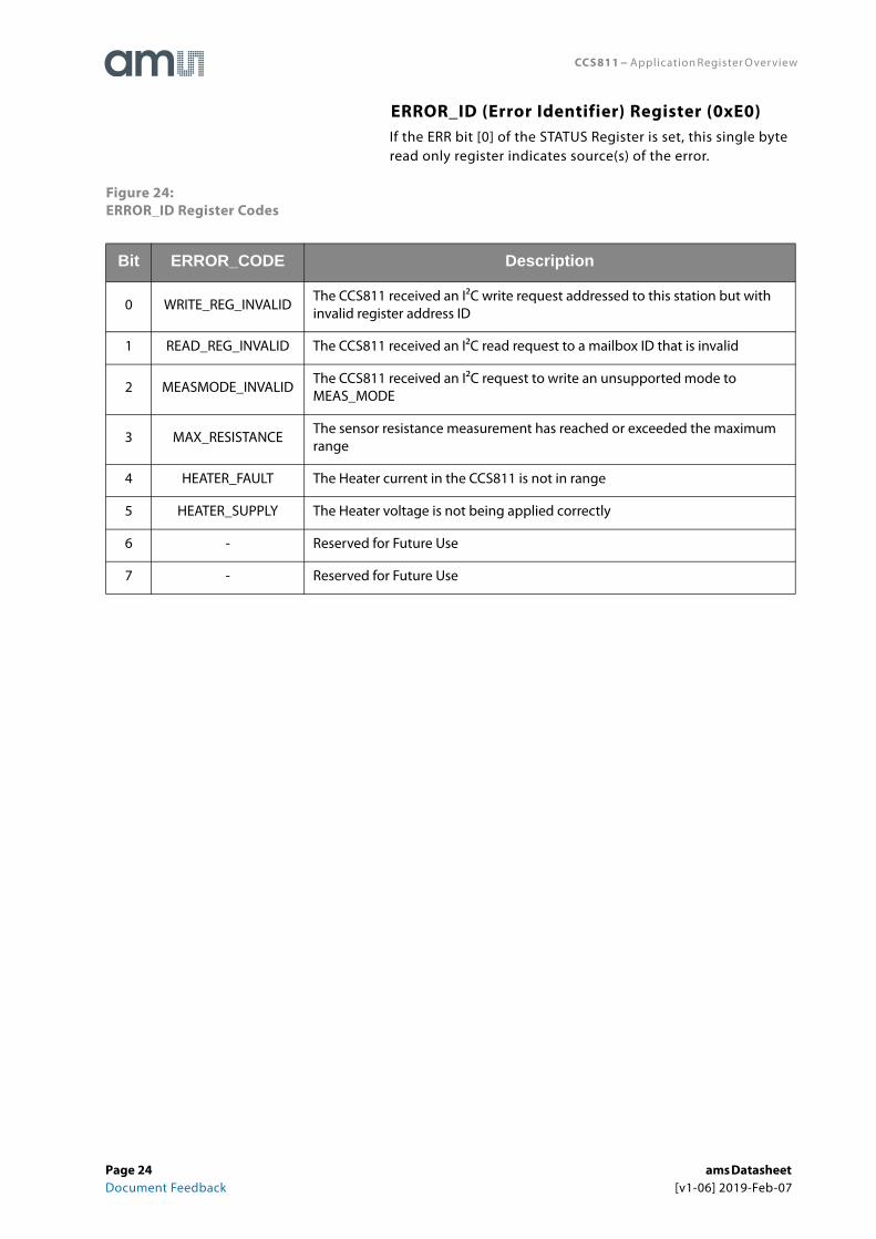
ERROR_ID (Error Identifier) Register (0xE0)If the ERR bit [0] of the STATUS Register is set, this single byte read only register indicates source(s) of the error.
Figure 24:ERROR_ID Register Codes
Bit ERROR_CODE Description
0 WRITE_REG_INVALIDThe CCS811 received an I²C write request addressed to this station but with invalid register address ID
1 READ_REG_INVALID The CCS811 received an I²C read request to a mailbox ID that is invalid
2 MEASMODE_INVALIDThe CCS811 received an I²C request to write an unsupported mode to MEAS_MODE
3 MAX_RESISTANCEThe sensor resistance measurement has reached or exceeded the maximum range
4 HEATER_FAULT The Heater current in the CCS811 is not in range
5 HEATER_SUPPLY The Heater voltage is not being applied correctly
6 - Reserved for Future Use
7 - Reserved for Future Use
Page 24 ams Datasheet Document Feedback [v1-06] 2019-Feb-07
CCS811 − Application Register Overview
SW_RESET Register (0xFF)As an alternative to Power-On reset or Hardware Reset a Software Reset is available.
Asserting the SW_RESET will restart the CCS811 in Boot mode to enable new application firmware to be downloaded.
To prevent accidental SW_RESET a sequence of four bytes must be written to this register in a single I²C sequence: 0x11, 0xE5, 0x72, 0x8A.
For details, please refer to application notes ams AN000369 and ams AN000371.
ams Datasheet Page 25[v1-06] 2019-Feb-07 Document Feedback
CCS811 − Bootloader Register Overview
All I²C transactions must use the (7bits) slave address 0x5A or 0x5B depending on status of ADDR pin when writing to and reading from the CCS811. Figure 25 shows the bootloader register map for CCS811.
Figure 25:CCS811 Bootloader Register Map
Note(s):
1. The number of bytes read from a register must not exceed the size in this table.
2. For more information on performing application code download please refer to application note ams AN000371.
Address Register R/W Size Description
0x00 STATUS R 1 byte Status register
0x20 HW_ID R 1 byte Hardware ID. The value is 0x81
0x21 HW Version R 1 byte Hardware Version. The value is 0x1X
0x23 FW_Boot_Version R 2 bytesFirmware Boot Version. The first 2 bytes contain the firmware version number for the boot code.
0x24 FW_App_Version R 2 bytesFirmware Application Version. The first 2 bytes contain the firmware version number for the application code.
0xE0 ERROR_ID R 1 byteError ID. When the status register reports an error it source is located in this register
0xF1 APP_ERASE W 4 bytesIf the correct 4 bytes (0xE7 0xA7 0xE6 0x09) are written to this register in a single sequence the device will start the application erase
0xF2 APP_DATA W 9 bytesTransmit flash code for the bootloader to write to the application flash code space.
0xF3 APP_VERIFY W -Starts the process of the bootloader checking though the application to make sure a full image is valid.
0xF4 APP_START W -
Application start. Used to transition the CCS811 state from boot to application mode, a write with no data is required. Before performing a write to APP_START the Status register should be accessed to check if there is a valid application present.
0xFF SW_RESET W 4 bytesIf the correct 4 bytes (0x11 0xE5 0x72 0x8A) are written to this register in a single sequence the device will reset and return to BOOT mode.
Bootloader Register Overview
Page 26 ams Datasheet Document Feedback [v1-06] 2019-Feb-07
CCS811 − Bootloader Register Overview
Registers not detailed below are documented in the Application Register Overview section.
APP_ERASE (Application Erase) Register (0xF1)To prevent accidental APP_ERASE a sequence of four bytes must be written to this register in a single I²C sequence: 0xE7, 0xA7, 0xE6, 0x09.
The APP_ERASE can take a variable amount of time. The status register can be polled to determine when this function is
complete. The 6th bit (0x40) is initialised to 0 and set to a 1 on completion of the APP_ERASE function. After an erase this bit is only cleared by doing a reset or starting the application.
APP_DATA (Application Data) Register (0xF2)Nine byte, write only register for sending small chunks of application data which will be written in order to the CCS811 flash code.
APP_VERIFY (Application Verify) Register (0xF3)Single byte write only register which starts the application verify process run by the bootloader to check for a complete application code image. Command only needs to be called once after a firmware download as the result is saved in a flash location that gets checked during device initialisation.
The APP_VERIFY can take a variable amount of time. The status register can be polled to determine when this function is
complete. The 5th bit (0x20) is initialised to 0 and set to a 1 on completion of the APP_VERIFY function. After an APP_VERIFY this bit is only cleared by doing a reset or starting the application.
For details on downloading new application firmware please refer to application note ams AN000371.
APP_START (Application Start) Register (0xF4)To change the mode of the CCS811 from Boot mode to running the application, a single byte write of 0xF4 is required.
The CCS811 interprets this as an address write to select the ‘APP_START’ register and starts running the loaded application software if it is a valid version (Refer to the STATUS Register (0x00)).
ams Datasheet Page 27[v1-06] 2019-Feb-07 Document Feedback
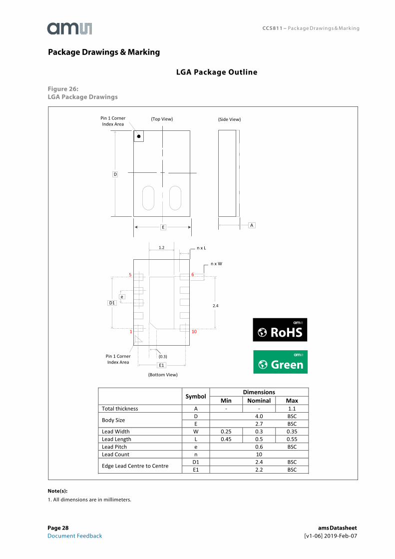
CCS811 − Package Drawings & Mark ing
LGA Package Outline
Figure 26:LGA Package Drawings
Note(s):
1. All dimensions are in millimeters.
Package Drawings & Marking
E
D
Pin 1 Corner Index Area
A
Pin 1 Corner Index Area
(Top View) (Side View)
D1
E1
e
1.2
2.4
n x W
n x L
(0.3)
(Bottom View)
1
5
10
6
Symbol Dimensions
Min Nominal Max Total thickness A - - 1.1
Body Size D 4.0 BSC E 2.7 BSC
Lead Width W 0.25 0.3 0.35 Lead Length L 0.45 0.5 0.55 Lead Pitch e 0.6 BSC Lead Count n 10
Edge Lead Centre to Centre D1 2.4 BSC E1 2.2 BSC
Green
RoHS
Page 28 ams Datasheet Document Feedback [v1-06] 2019-Feb-07
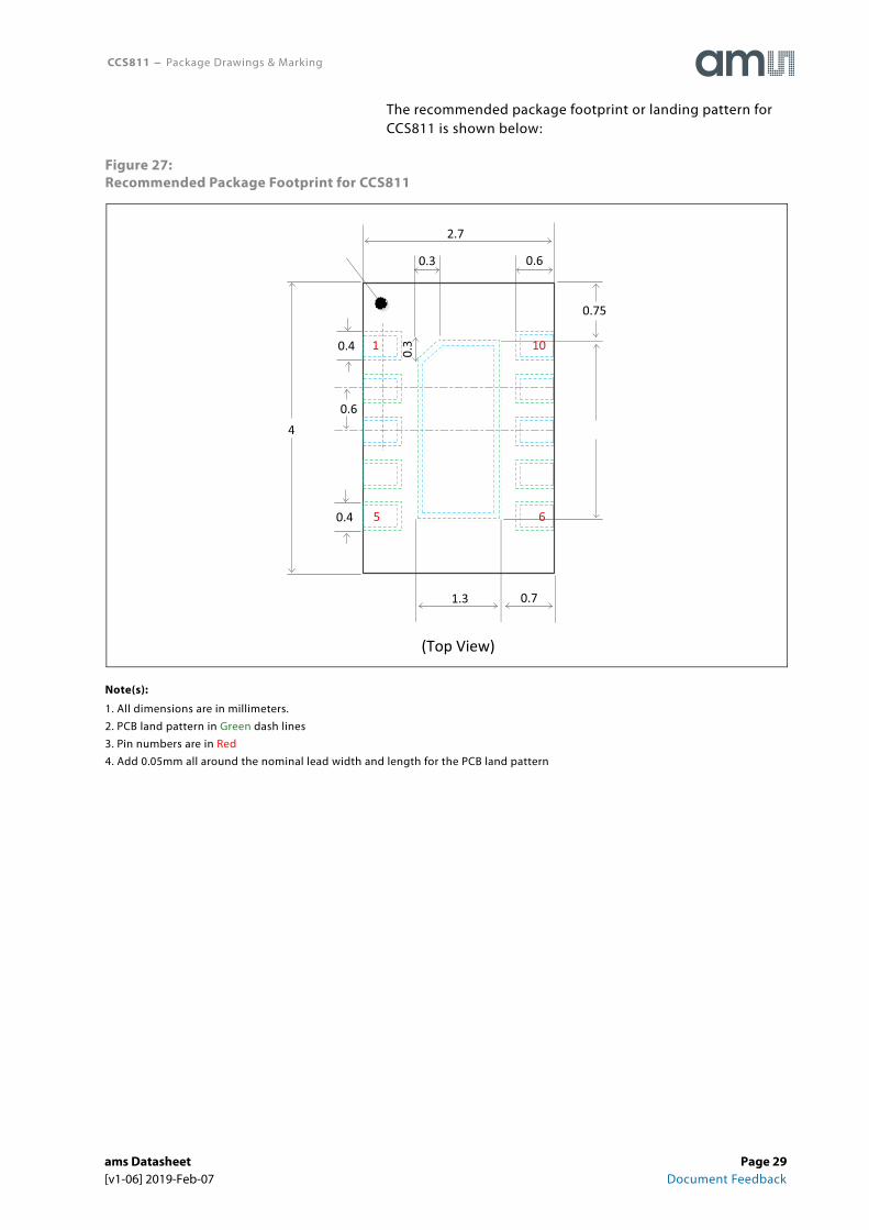
CCS811 − Package Drawings & Marking
The recommended package footprint or landing pattern for CCS811 is shown below:
Figure 27:Recommended Package Footprint for CCS811
Note(s):
1. All dimensions are in millimeters.
2. PCB land pattern in Green dash lines
3. Pin numbers are in Red
4. Add 0.05mm all around the nominal lead width and length for the PCB land pattern
40.6
1.3
0.6
2.7
0.4
0.4
5
1
6
10
(Top View)
0.75
0.7
0.3
0.3
ams Datasheet Page 29[v1-06] 2019-Feb-07 Document Feedback
CCS811 − Ordering & Contact Information
Figure 28:Ordering Information
Note(s):
1. Refer to JEDEC J-STD020 lead-free standard for typical soldering reflow profile
Technical Support is available at:www.ams.com/Technical-Support
Provide feedback about this document at:www.ams.com/Document-Feedback
For further information and requests, e-mail us at:[email protected]
For sales offices, distributors and representatives, please visit: www.ams.com/Contact
Headquartersams AGTobelbader Strasse 308141 PremstaettenAustria, Europe
Tel: +43 (0) 3136 500 0
Website: www.ams.com
Ordering Code Description Package MOQ
CCS811B-JOPR5K CCS811 digital gas sensor for Indoor Air Quality Monitoring
2.7mm x 4.0mm x 1.1mm LGA 5000
CCS811B-JOPD500CCS811 digital gas sensor for Indoor Air Quality Monitoring
2.7mm x 4.0mm x 1.1mm LGA 500
Ordering & Contact Information
Page 30 ams Datasheet Document Feedback [v1-06] 2019-Feb-07
CCS811 − RoHS Compliant & ams Green Statement
RoHS: The term RoHS compliant means that ams AG products fully comply with current RoHS directives. Our semiconductor products do not contain any chemicals for all 6 substance categories, including the requirement that lead not exceed 0.1% by weight in homogeneous materials. Where designed to be soldered at high temperatures, RoHS compliant products are suitable for use in specified lead-free processes.
ams Green (RoHS compliant and no Sb/Br): ams Green defines that in addition to RoHS compliance, our products are free of Bromine (Br) and Antimony (Sb) based flame retardants (Br or Sb do not exceed 0.1% by weight in homogeneous material).
Important Information: The information provided in this statement represents ams AG knowledge and belief as of the date that it is provided. ams AG bases its knowledge and belief on information provided by third parties, and makes no representation or warranty as to the accuracy of such information. Efforts are underway to better integrate information from third parties. ams AG has taken and continues to take reasonable steps to provide representative and accurate information but may not have conducted destructive testing or chemical analysis on incoming materials and chemicals. ams AG and ams AG suppliers consider certain information to be proprietary, and thus CAS numbers and other limited information may not be available for release.
RoHS Compliant & ams Green Statement
ams Datasheet Page 31[v1-06] 2019-Feb-07 Document Feedback
CCS811 − Copyrights & Disclaimer
Copyright ams AG, Tobelbader Strasse 30, 8141 Premstaetten, Austria-Europe. Trademarks Registered. All rights reserved. The material herein may not be reproduced, adapted, merged, translated, stored, or used without the prior written consent of the copyright owner.
Devices sold by ams AG are covered by the warranty and patent indemnification provisions appearing in its General Terms of Trade. ams AG makes no warranty, express, statutory, implied, or by description regarding the information set forth herein. ams AG reserves the right to change specifications and prices at any time and without notice. Therefore, prior to designing this product into a system, it is necessary to check with ams AG for current information. This product is intended for use in commercial applications. Applications requiring extended temperature range, unusual environmental requirements, or high reliability applications, such as military, medical life-support or life-sustaining equipment are specifically not recommended without additional processing by ams AG for each application. This product is provided by ams AG “AS IS” and any express or implied warranties, including, but not limited to the implied warranties of merchantability and fitness for a particular purpose are disclaimed.
ams AG shall not be liable to recipient or any third party for any damages, including but not limited to personal injury, property damage, loss of profits, loss of use, interruption of business or indirect, special, incidental or consequential damages, of any kind, in connection with or arising out of the furnishing, performance or use of the technical data herein. No obligation or liability to recipient or any third party shall arise or flow out of ams AG rendering of technical or other services.
Copyrights & Disclaimer
Page 32 ams Datasheet Document Feedback [v1-06] 2019-Feb-07
CCS811 − Document Status
Document Status Product Status Definition
Product Preview Pre-Development
Information in this datasheet is based on product ideas in the planning phase of development. All specifications are design goals without any warranty and are subject to change without notice
Preliminary Datasheet Pre-Production
Information in this datasheet is based on products in the design, validation or qualification phase of development. The performance and parameters shown in this document are preliminary without any warranty and are subject to change without notice
Datasheet Production
Information in this datasheet is based on products in ramp-up to full production or full production which conform to specifications in accordance with the terms of ams AG standard warranty as given in the General Terms of Trade
Datasheet (discontinued) Discontinued
Information in this datasheet is based on products which conform to specifications in accordance with the terms of ams AG standard warranty as given in the General Terms of Trade, but these products have been superseded and should not be used for new designs
Document Status
ams Datasheet Page 33[v1-06] 2019-Feb-07 Document Feedback
CCS811 − Revision Information
Note(s):
1. Page and figure numbers for the previous version may differ from page and figure numbers in the current revision.
2. Correction of typographical errors is not explicitly mentioned.
Changes from 1-05 (2018-May-01) to current revision 1-06 (2019-Feb-07) Page
Updated figure 6 6
Updated figure 7 7
Added figure 8 8
Added “State Machine” under “Detailed Description” 9
Added “Power States” under “Detailed Description” 10
Updated and Renamed “Early-Life Use (Burn-In)” to “Early-Life (Burn-In)” 12
Updated Conditioning Period (Run-In), eCO2, Temperature and Humidity Compensation 12
Updated figure 11 and notes under it 14
Updated figure 15 18
Updated “FW_App_Version (Firmware Application Version) Register (0x24)” 23
Revision Information
Page 34 ams Datasheet Document Feedback [v1-06] 2019-Feb-07
CCS811 − Appendix
References
Figure 29:Document Reference
Document Reference Description
ams AN000367 CCS811 Assembly guidelines
ams AN000368 CCS811 Design guidelines
ams AN000369 CCS811 Programming and interfacing guide
ams AN000370 CCS811 Clean air baseline save and restore
ams AN000371 CCS811 Performing a firmware download
ams AN000373 CCS811 Factory test procedure
Appendix
ams Datasheet Page 35[v1-06] 2019-Feb-07 Document Feedback
CCS811 − Content Guide
1 General Description2 Key Benefits & Features2 Applications3 Block Diagram
4 Pin Assignment5 Absolute Maximum Ratings6 Electrical Characteristics
9 Detailed Description9 State Machine10 Power States11 Modes of Operation11 Early-Life (Burn-In)12 Conditioning Period (Run-In)12 eCO212 eTVOC12 Temperature and Humidity Compensation12 Interrupt and Interrupt on Threshold13 Automatic Baseline Correction13 Manual Baseline Correction
14 Application Information14 Host System Software Requirements15 I²C Interface15 I²C Register Write16 I²C Register Read
17 Application Register Overview18 STATUS Register (0x00)19 MEAS_MODE (Measurement and Conditions) Register
(0x01)20 ALG_RESULT_DATA (Algorithm Results Data) Register
(0x02)20 RAW_DATA Register (0x03)21 ENV_DATA (Environment Data) Register (0x05)21 Relative Humidity22 THRESHOLDS Register (0x10)22 BASELINE Register (0x11)22 HW_ID (Hardware identifier) Register (0x20)22 HW_Version (Hardware Version) Register (0x21)23 FW_Boot_Version (Firmware Bootloader Version) Regis-
ter (0x23)23 FW_App_Version (Firmware Application Version) Regis-
ter (0x24)24 ERROR_ID (Error Identifier) Register (0xE0)25 SW_RESET Register (0xFF)
26 Bootloader Register Overview27 APP_ERASE (Application Erase) Register (0xF1)27 APP_DATA (Application Data) Register (0xF2)27 APP_VERIFY (Application Verify) Register (0xF3)27 APP_START (Application Start) Register (0xF4)
Content Guide
Page 36 ams Datasheet Document Feedback [v1-06] 2019-Feb-07
CCS811 − Content Guide
28 Package Drawings & Marking28 LGA Package Outline
30 Ordering & Contact Information31 RoHS Compliant & ams Green Statement32 Copyrights & Disclaimer33 Document Status34 Revision Information
35 Appendix35 References
ams Datasheet Page 37[v1-06] 2019-Feb-07 Document Feedback


![tbd - Adafruit Industries · 2017. 8. 1. · Page 6 ams Datasheet Document Feedback [v1-00] 2016-Dec-23 CCS811 − Electrical Characterstii cs Figure 6: Electrical Characteristics](https://img.pdfslide.net/doc/110x75/60b89aae33dbea16207e2ade/tbd-adafruit-industries-2017-8-1-page-6-ams-datasheet-document-feedback-v1-00.jpg)