Embed Size (px)
Citation preview
1Subject to change without notice.www.cree.com/RF
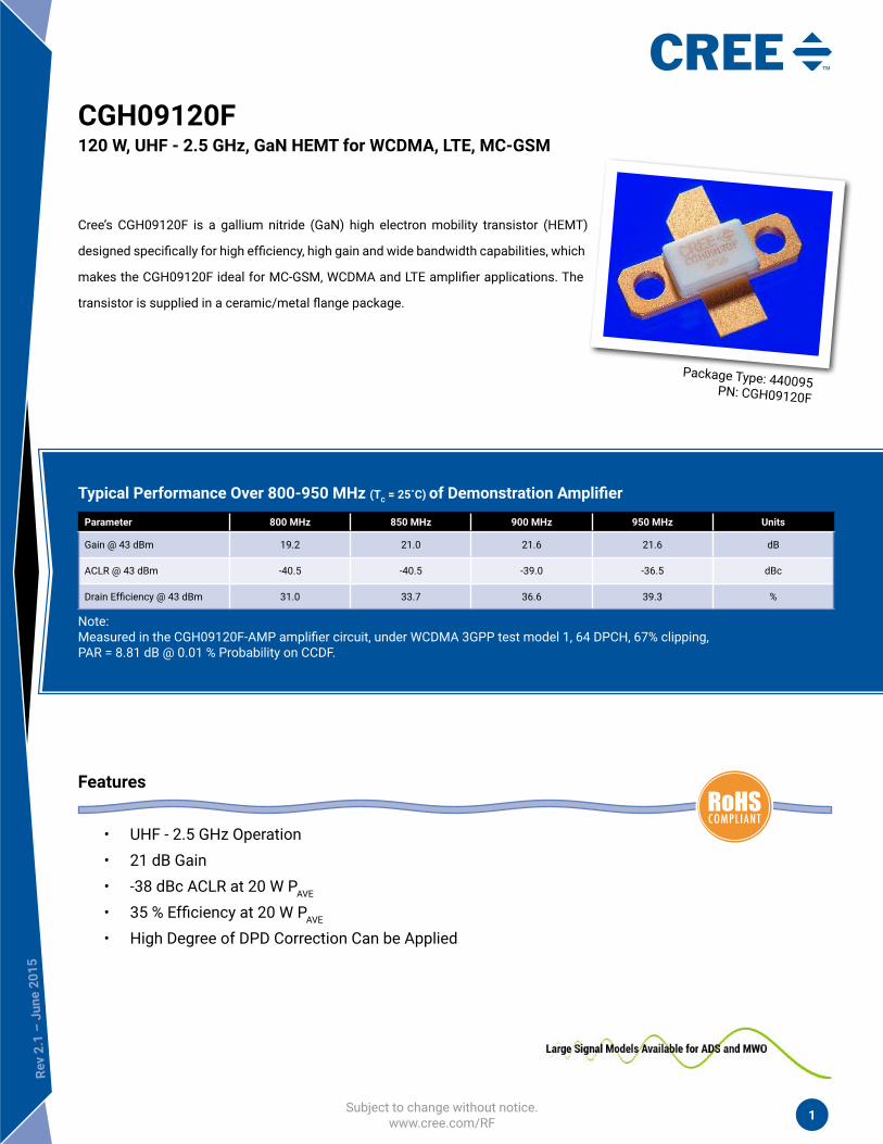
CGH09120F120 W, UHF - 2.5 GHz, GaN HEMT for WCDMA, LTE, MC-GSM
Cree’s CGH09120F is a gallium nitride (GaN) high electron mobility transistor (HEMT)
designed specifically for high efficiency, high gain and wide bandwidth capabilities, which
makes the CGH09120F ideal for MC-GSM, WCDMA and LTE amplifier applications. The
transistor is supplied in a ceramic/metal flange package.
Package Type: 440095PN: CGH09120F
Rev
2.1
– Ju
ne 2
015
Features
• UHF - 2.5 GHz Operation • 21 dB Gain• -38 dBc ACLR at 20 W PAVE
• 35 % Efficiency at 20 W PAVE
• High Degree of DPD Correction Can be Applied
Typical Performance Over 800-950 MHz (TC = 25˚C) of Demonstration Amplifier
Parameter 800 MHz 850 MHz 900 MHz 950 MHz Units
Gain @ 43 dBm 19.2 21.0 21.6 21.6 dB
ACLR @ 43 dBm -40.5 -40.5 -39.0 -36.5 dBc
Drain Efficiency @ 43 dBm 31.0 33.7 36.6 39.3 %
Note:Measured in the CGH09120F-AMP amplifier circuit, under WCDMA 3GPP test model 1, 64 DPCH, 67% clipping,PAR = 8.81 dB @ 0.01 % Probability on CCDF.
2 CGH09120F Rev 2.1
Cree, Inc.4600 Silicon Drive
Durham, North Carolina, USA 27703USA Tel: +1.919.313.5300
Fax: +1.919.869.2733www.cree.com/rf
Copyright © 2009-2015 Cree, Inc. All rights reserved. The information in this document is subject to change without notice. Cree and the Cree logo are registered trademarks of Cree, Inc.
Absolute Maximum Ratings (not simultaneous) at 25˚C Case Temperature
Parameter Symbol Rating Units Conditions
Drain-Source Voltage VDSS 84 Volts 25˚C
Gate-to-Source Voltage VGS -10, +2 Volts 25˚C
Power Dissipation PDISS 56 Watts
Storage Temperature TSTG -65, +150 ˚C
Operating Junction Temperature TJ 225 ˚C
Maximum Forward Gate Current IGMAX 30 mA 25˚C
Maximum Drain Current1 IDMAX 12 A 25˚C
Soldering Temperature2 TS 245 ˚C
Screw Torque τ 80 in-oz
Thermal Resistance, Junction to Case3 RθJC 1.7 ˚C/W 85˚C
Case Operating Temperature3 TC -40, +150 ˚C
Note:1 Current limit for long term, reliable operation.2 Refer to the Application Note on soldering at www.cree.com/RF/Document-Library3 Measured for the CGH09120F at PDISS = 56 W
Electrical Characteristics (TC = 25˚C)
Characteristics Symbol Min. Typ. Max. Units Conditions
DC Characteristics1
Gate Threshold Voltage VGS(th) -3.8 -3.0 -2.3 VDC VDS = 10 V, ID = 28.8 mA
Gate Quiescent Voltage VGS(Q) – -2.7 – VDC VDS = 28 V, ID = 1.2 A
Saturated Drain Current2 IDS 23.2 28.0 – A VDS = 6.0 V, VGS = 2.0 V
Drain-Source Breakdown Voltage VBR 120 – – VDC VGS = -8 V, ID = 28.8 mA
RF Characteristics5 (TC = 25˚C, F0 = 870 MHz unless otherwise noted)
Saturated Output Power3,4 PSAT – 120 – W VDD = 28 V, IDQ = 1.2 A,
Pulsed Drain Efficiency3 η – 75 – % VDD = 28 V, IDQ = 1.2 A, POUT = PSAT
Modulated Gain6 GSS 20 21.5 – dB VDD = 28 V, IDQ = 1.2 A, POUT = 43 dBm
WCDMA Linearity6 ACLR – -38 –34 dBc VDD = 28 V, IDQ = 1.2 A, POUT = 43 dBm
Modulated Drain Efficiency6 η 31 35 – % VDD = 28 V, IDQ = 1.2 A, POUT = 43 dBm
Output Mismatch Stress VSWR – – 10 : 1 YNo damage at all phase angles, VDD = 28 V, IDQ = 1.2 A, POUT = 20 W CW
Dynamic Characteristics
Input Capacitance CGS – 35.3 – pF VDS = 28 V, Vgs = -8 V, f = 1 MHz
Output Capacitance CDS – 9.1 – pF VDS = 28 V, Vgs = -8 V, f = 1 MHz
Feedback Capacitance CGD – 1.6 – pF VDS = 28 V, Vgs = -8 V, f = 1 MHz
Notes:1 Measured on wafer prior to packaging.2 Scaled from PCM data.3 Pulse Width = 40 μS, Duty Cycle = 5 %.4 PSAT is defined as IG = 10 mA peak.5 Measured in CGH09120F-AMP6 Single Carrier WCDMA, 3GPP Test Model 1, 64 DPCH, 67 % Clipping, PAR = 8.81 dB @ 0.01 % Probability on CCDF.
3 CGH09120F Rev 2.1
Cree, Inc.4600 Silicon Drive
Durham, North Carolina, USA 27703USA Tel: +1.919.313.5300
Fax: +1.919.869.2733www.cree.com/rf
Copyright © 2009-2015 Cree, Inc. All rights reserved. The information in this document is subject to change without notice. Cree and the Cree logo are registered trademarks of Cree, Inc.
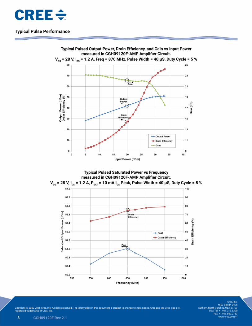
Typical Pulse Performance
Typical Pulsed Output Power, Drain Efficiency, and Gain vs Input Power measured in CGH09120F-AMP Amplifier Circuit.
VDS = 28 V, IDS = 1.2 A, Freq = 870 MHz, Pulse Width = 40 μS, Duty Cycle = 5 %
Typical Pulsed Saturated Power vs Frequencymeasured in CGH09120F-AMP Amplifier Circuit.
VDS = 28 V, IDS = 1.2 A, PSAT = 10 mA IGS Peak, Pulse Width = 40 μS, Duty Cycle = 5 %
50
60
70
80
90
100
52.0
52.4
52.8
53.2
53.6
54.0D
rain
Effic
ienc
y(%
)
Satu
rate
dO
utpu
tPow
er(d
Bm
)
Psat
DrainEfficiency
0
10
20
30
40
50
50.0
50.4
50.8
51.2
51.6
52.0
700 750 800 850 900 950 1000
Dra
inEf
ficie
ncy
(%)
Satu
rate
dO
utpu
tPow
er(d
Bm
)
Frequency (MHz)
Psat
Drain Efficiency
Psat
17
19
21
23
25
40
50
60
70
80
Gai
n(d
B)
Out
putP
ower
(dB
m)
Dra
inEf
ficie
ncy
(%)
Gain
OutputPower
9
11
13
15
17
0
10
20
30
40
0 5 10 15 20 25 30 35 40
Gai
n(d
B)
Out
putP
ower
(dB
m)
Dra
inEf
ficie
ncy
(%)
Input Power (dBm)
Output Power
Drain Efficiency
Gain
DrainEfficiency
4 CGH09120F Rev 2.1
Cree, Inc.4600 Silicon Drive
Durham, North Carolina, USA 27703USA Tel: +1.919.313.5300
Fax: +1.919.869.2733www.cree.com/rf
Copyright © 2009-2015 Cree, Inc. All rights reserved. The information in this document is subject to change without notice. Cree and the Cree logo are registered trademarks of Cree, Inc.
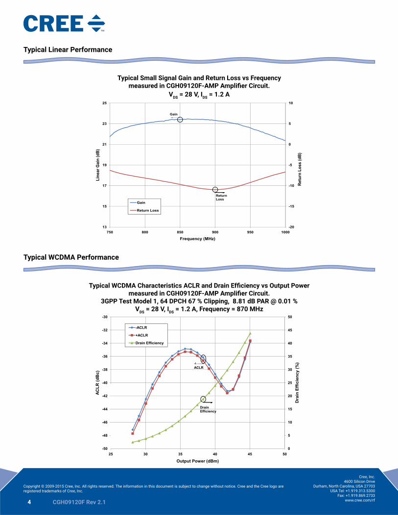
Typical Linear Performance
Typical Small Signal Gain and Return Loss vs Frequencymeasured in CGH09120F-AMP Amplifier Circuit.
VDS = 28 V, IDS = 1.2 A
Typical WCDMA Performance
Typical WCDMA Characteristics ACLR and Drain Efficiency vs Output Powermeasured in CGH09120F-AMP Amplifier Circuit.
3GPP Test Model 1, 64 DPCH 67 % Clipping, 8.81 dB PAR @ 0.01 %VDS = 28 V, IDS = 1.2 A, Frequency = 870 MHz
25
30
35
40
45
50
-40
-38
-36
-34
-32
-30
Dra
inEf
ficie
ncy
(%)
AC
LR(d
Bc)
-ACLR
+ACLR
Drain Efficiency
ACLR
0
5
10
15
20
25
-50
-48
-46
-44
-42
-40
25 30 35 40 45 50
Dra
inEf
ficie
ncy
(%)
AC
LR(d
Bc)
Output Power (dBm)
DrainEfficiency
-5
0
5
10
19
21
23
25
Retu
rnLo
ss(d
B)
Line
arG
ain
(dB)
Gain
-20
-15
-10
-5
13
15
17
19
750 800 850 900 950 1000
Retu
rnLo
ss(d
B)
Line
arG
ain
(dB)
Frequency (MHz)
Gain
Return Loss
ReturnLoss
5 CGH09120F Rev 2.1
Cree, Inc.4600 Silicon Drive
Durham, North Carolina, USA 27703USA Tel: +1.919.313.5300
Fax: +1.919.869.2733www.cree.com/rf
Copyright © 2009-2015 Cree, Inc. All rights reserved. The information in this document is subject to change without notice. Cree and the Cree logo are registered trademarks of Cree, Inc.
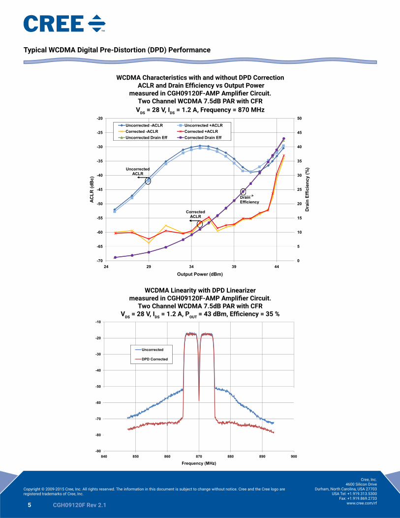
Typical WCDMA Digital Pre-Distortion (DPD) Performance
WCDMA Characteristics with and without DPD Correction ACLR and Drain Efficiency vs Output Power
measured in CGH09120F-AMP Amplifier Circuit.Two Channel WCDMA 7.5dB PAR with CFR
VDS = 28 V, IDS = 1.2 A, Frequency = 870 MHz
WCDMA Linearity with DPD Linearizer measured in CGH09120F-AMP Amplifier Circuit.
Two Channel WCDMA 7.5dB PAR with CFRVDS = 28 V, IDS = 1.2 A, POUT = 43 dBm, Efficiency = 35 %
25
30
35
40
45
50
-45
-40
-35
-30
-25
-20
Dra
inEf
ficie
ncy
(%)
AC
LR(d
Bc)
Uncorrected -ACLR Uncorrected +ACLRCorrected -ACLR Corrected +ACLRUncorrected Drain Eff Corrected Drain Eff
UncorrectedACLR
0
5
10
15
20
25
-70
-65
-60
-55
-50
-45
24 29 34 39 44
Dra
inEf
ficie
ncy
(%)
AC
LR(d
Bc)
Output Power (dBm)
CorrectedACLR
DrainEfficiency
-50
-40
-30
-20
-10
Uncorrected
DPD Corrected
-90
-80
-70
-60
-50
840 850 860 870 880 890 900
Frequency (MHz)
6 CGH09120F Rev 2.1
Cree, Inc.4600 Silicon Drive
Durham, North Carolina, USA 27703USA Tel: +1.919.313.5300
Fax: +1.919.869.2733www.cree.com/rf
Copyright © 2009-2015 Cree, Inc. All rights reserved. The information in this document is subject to change without notice. Cree and the Cree logo are registered trademarks of Cree, Inc.
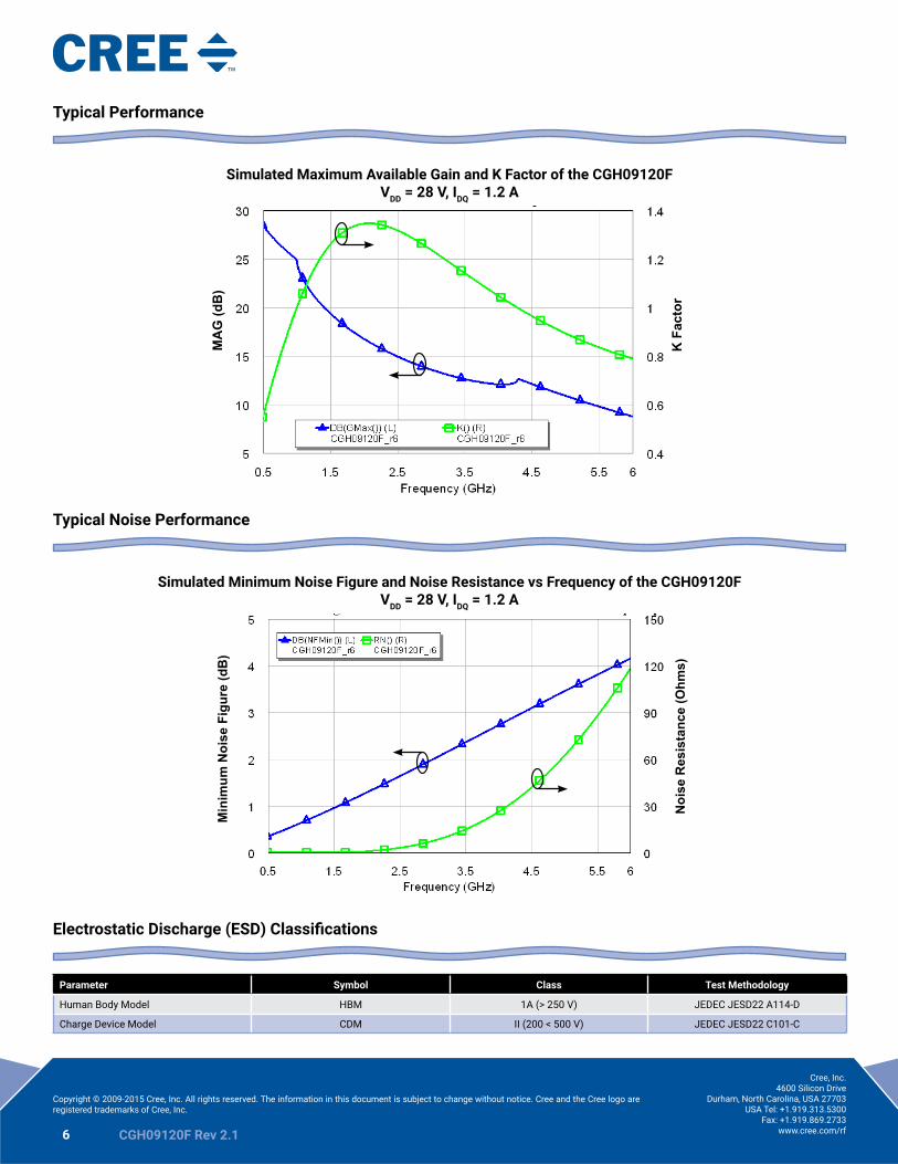
Typical Performance
Simulated Maximum Available Gain and K Factor of the CGH09120FVDD = 28 V, IDQ = 1.2 A
Typical Noise Performance
Simulated Minimum Noise Figure and Noise Resistance vs Frequency of the CGH09120FVDD = 28 V, IDQ = 1.2 A
Electrostatic Discharge (ESD) Classifications
Parameter Symbol Class Test Methodology
Human Body Model HBM 1A (> 250 V) JEDEC JESD22 A114-D
Charge Device Model CDM II (200 < 500 V) JEDEC JESD22 C101-C
Min
imum
Noi
se F
igur
e (d
B)
Noi
se R
esis
tanc
e (O
hms)
MA
G (d
B)
K F
acto
r
7 CGH09120F Rev 2.1
Cree, Inc.4600 Silicon Drive
Durham, North Carolina, USA 27703USA Tel: +1.919.313.5300
Fax: +1.919.869.2733www.cree.com/rf
Copyright © 2009-2015 Cree, Inc. All rights reserved. The information in this document is subject to change without notice. Cree and the Cree logo are registered trademarks of Cree, Inc.
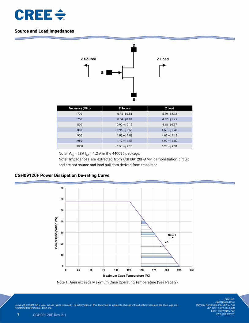
Source and Load Impedances
Frequency (MHz) Z Source Z Load
700 0.75 - j 0.58 5.59 - j 2.12
750 0.84 - j 0.18 4.97 - j 1.25
800 0.90 + j 0.19 4.68 - j 0.37
850 0.95 + j 0.59 4.59 + j 0.45
900 1.02 + j 1.03 4.67 + j 1.19
950 1.17 + j 1.53 4.90 + j 1.82
1000 1.53 + j 2.10 5.28 + j 2.31
Note1 VDD = 28V, IDQ = 1.2 A in the 440095 package.Note2 Impedances are extracted from CGH09120F-AMP demonstration circuit and are not source and load pull data derived from transistor.
CGH09120F Power Dissipation De-rating Curve
Note 1. Area exceeds Maximum Case Operating Temperature (See Page 2).
D
Z Source Z Load
G
S
40
50
60
70
Pow
erD
issi
patio
n(W
)
CGH09120F Average Power Dissipation De-rating Curve
0
10
20
30
40
0 25 50 75 100 125 150 175 200 225 250
Pow
erD
issi
patio
n(W
)
Maximum Case Temperature (°C)
Note 1
8 CGH09120F Rev 2.1
Cree, Inc.4600 Silicon Drive
Durham, North Carolina, USA 27703USA Tel: +1.919.313.5300
Fax: +1.919.869.2733www.cree.com/rf
Copyright © 2009-2015 Cree, Inc. All rights reserved. The information in this document is subject to change without notice. Cree and the Cree logo are registered trademarks of Cree, Inc.
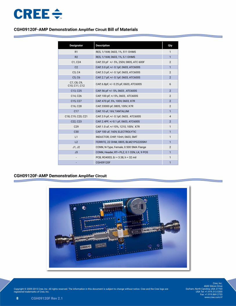
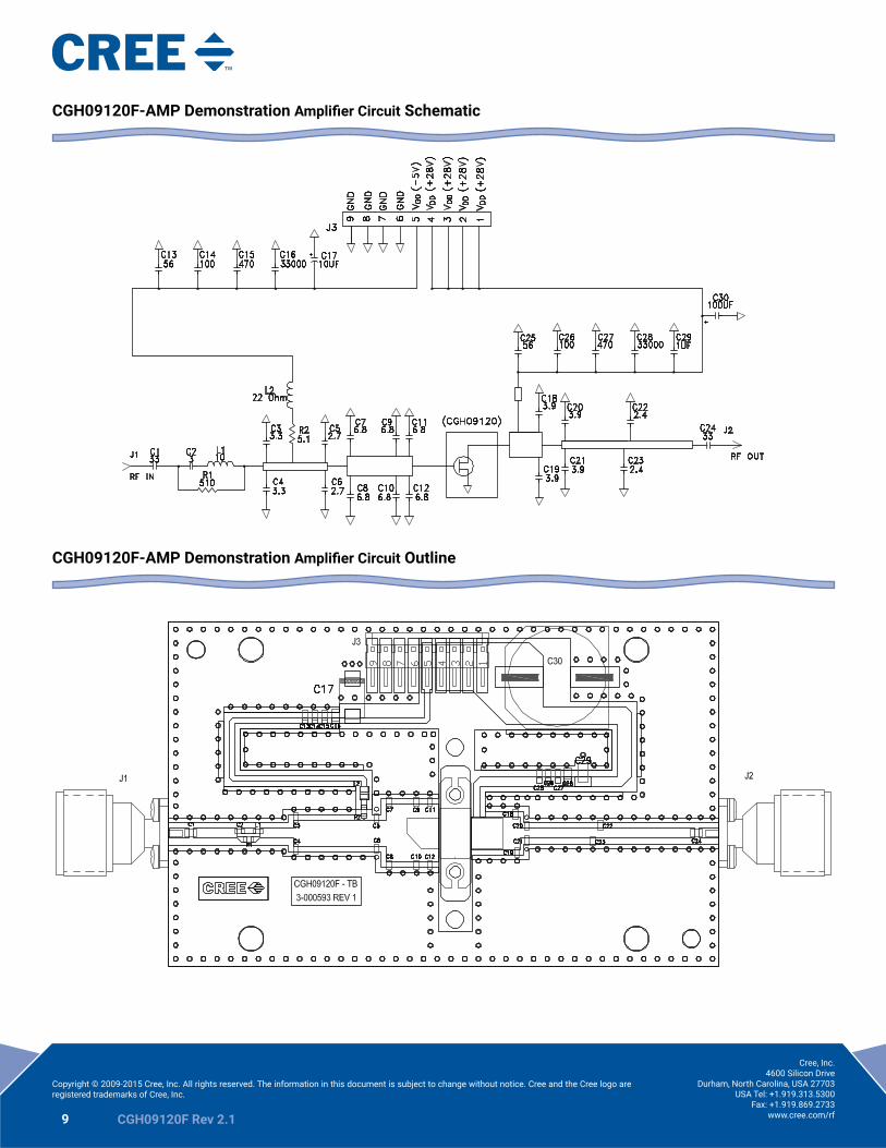
CGH09120F-AMP Demonstration Amplifier Circuit Bill of Materials
Designator Description Qty
R1 RES, 1/16W, 0603, 1%, 511 OHMS 1
R2 RES, 1/16W, 0603, 1%, 5.1 OHMS 1
C1, C24 CAP, 33 pF +/- 5%, 250V, 0805, ATC 600F 2
C2 CAP, 3.0 pF, +/- 0.1pF, 0603, ATC600S 1
C3, C4 CAP, 3.3 pF, +/- 0.1pF, 0603, ATC600S 2
C5, C6 CAP, 2.7 pF, +/- 0.1pF, 0603, ATC600S 2
C7, C8, C9, C10, C11, C12 CAP, 6.8pF, +/- 0.25 pF, 0603, ATC600S 6
C13, C25 CAP, 56 pF +/- 5%, 0603 , ATC600S 2
C14, C26 CAP, 100 pF, +/-5%, 0603, ATC600S 2
C15, C27 CAP, 470 pF, 5%, 100V, 0603, X7R 2
C16, C28 CAP, 33000 pF, 0805, 100V, X7R 2
C17 CAP, 10 uF, 16V, TANTALUM 1
C18, C19, C20, C21 CAP, 3.9 pF, +/- 0.1pF, 0603, ATC600S 4
C22, C23 CAP, 2.4PF, +/-0.1 pF, 0603, ATC600S 2
C29 CAP, 1.0 uF, +/-10%, 1210, 100V, X7R 1
C30 CAP 100 uF, 160V, ELECTROLYTIC 1
L1 INDUCTOR, CHIP, 10nH, 0603, SMT 1
L2 FERRITE, 22 OHM, 0805, BLM21PG220SN1 1
J1, J2 CONN, N-Type, Female, 0.500 SMA Flange 2
J3 CONN, Header, RT> PLZ, 0.1 CEN, LK, 9 POS 1
- PCB, RO4003, Er = 3.38, h = 32 mil 1
- CGH09120F 1
CGH09120F-AMP Demonstration Amplifier Circuit
9 CGH09120F Rev 2.1
Cree, Inc.4600 Silicon Drive
Durham, North Carolina, USA 27703USA Tel: +1.919.313.5300
Fax: +1.919.869.2733www.cree.com/rf
Copyright © 2009-2015 Cree, Inc. All rights reserved. The information in this document is subject to change without notice. Cree and the Cree logo are registered trademarks of Cree, Inc.
CGH09120F-AMP Demonstration Amplifier Circuit Schematic
CGH09120F-AMP Demonstration Amplifier Circuit Outline
10 CGH09120F Rev 2.1
Cree, Inc.4600 Silicon Drive
Durham, North Carolina, USA 27703USA Tel: +1.919.313.5300
Fax: +1.919.869.2733www.cree.com/rf
Copyright © 2009-2015 Cree, Inc. All rights reserved. The information in this document is subject to change without notice. Cree and the Cree logo are registered trademarks of Cree, Inc.
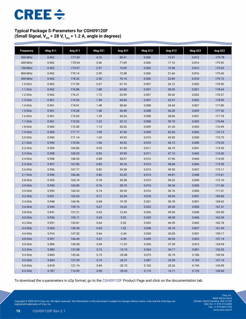
Typical Package S-Parameters for CGH09120F(Small Signal, VDS = 28 V, IDQ = 1.2 A, angle in degrees)
Frequency Mag S11 Ang S11 Mag S21 Ang S21 Mag S12 Ang S12 Mag S22 Ang S22
500 MHz 0.962 -177.69 4.16 80.41 0.006 15.01 0.812 -179.78
600 MHz 0.962 -178.94 3.46 77.69 0.006 17.16 0.814 179.92
700 MHz 0.962 -179.97 2.97 75.09 0.006 19.38 0.815 179.65
800 MHz 0.962 179.14 2.59 72.58 0.006 21.64 0.816 179.40
900 MHz 0.962 178.33 2.30 70.14 0.006 23.89 0.818 179.15
1.0 GHz 0.962 177.59 2.07 67.74 0.007 26.12 0.820 178.90
1.1 GHz 0.962 176.88 1.88 65.40 0.007 28.30 0.821 178.64
1.2 GHz 0.962 176.21 1.73 63.09 0.007 30.42 0.823 178.37
1.3 GHz 0.961 175.55 1.59 60.83 0.007 32.47 0.825 178.09
1.4 GHz 0.961 174.91 1.48 58.60 0.008 34.43 0.827 177.80
1.5 GHz 0.961 174.28 1.38 56.40 0.008 36.30 0.829 177.50
1.6 GHz 0.961 173.65 1.29 54.24 0.008 38.06 0.831 177.18
1.7 GHz 0.961 173.02 1.22 52.12 0.008 39.70 0.833 176.84
1.8 GHz 0.960 172.40 1.15 50.02 0.009 41.24 0.835 176.49
1.9 GHz 0.960 171.77 1.09 47.96 0.009 42.65 0.836 176.13
2.0 GHz 0.960 171.14 1.04 45.93 0.010 43.95 0.838 175.75
2.1 GHz 0.959 170.50 1.00 43.92 0.010 45.13 0.840 175.35
2.2 GHz 0.959 169.86 0.95 41.94 0.011 46.19 0.841 174.93
2.3 GHz 0.958 169.20 0.92 39.99 0.011 47.13 0.843 174.50
2.4 GHz 0.958 168.54 0.88 38.07 0.012 47.96 0.844 174.05
2.5 GHz 0.957 167.86 0.85 36.16 0.013 48.68 0.846 173.59
2.6 GHz 0.956 167.17 0.82 34.28 0.013 49.30 0.847 173.11
2.7 GHz 0.956 166.46 0.80 32.42 0.014 49.81 0.848 172.61
2.8 GHz 0.955 165.74 0.78 30.58 0.015 50.22 0.849 172.10
2.9 GHz 0.954 165.00 0.76 28.75 0.015 50.54 0.850 171.56
3.0 GHz 0.953 164.24 0.74 26.94 0.016 50.76 0.850 171.01
3.2 GHz 0.951 162.65 0.71 23.34 0.018 50.94 0.851 169.86
3.4 GHz 0.948 160.96 0.68 19.78 0.021 50.78 0.851 168.62
3.6 GHz 0.945 159.15 0.67 16.22 0.023 50.30 0.850 167.31
3.8 GHz 0.941 157.21 0.65 12.64 0.026 49.50 0.848 165.90
4.0 GHz 0.936 155.11 0.65 9.02 0.029 48.38 0.846 164.39
4.2 GHz 0.931 152.81 0.64 5.33 0.033 46.95 0.842 162.78
4.4 GHz 0.924 150.30 0.65 1.52 0.038 45.18 0.837 161.04
4.6 GHz 0.916 147.52 0.66 -2.44 0.043 43.05 0.831 159.17
4.8 GHz 0.907 144.44 0.67 -6.59 0.049 40.54 0.823 157.14
5.0 GHz 0.896 140.98 0.69 -11.01 0.056 37.59 0.813 154.94
5.2 GHz 0.882 137.08 0.72 -15.75 0.065 34.17 0.801 152.55
5.4 GHz 0.865 132.66 0.75 -20.88 0.075 30.19 0.786 149.94
5.6 GHz 0.844 127.59 0.79 -26.51 0.087 25.59 0.769 147.10
5.8 GHz 0.818 121.74 0.84 -32.73 0.102 20.26 0.749 143.99
6.0 GHz 0.787 114.95 0.90 -39.65 0.119 14.11 0.725 140.60
To download the s-parameters in s2p format, go to the CGH09120F Product Page and click on the documentation tab.
11 CGH09120F Rev 2.1
Cree, Inc.4600 Silicon Drive
Durham, North Carolina, USA 27703USA Tel: +1.919.313.5300
Fax: +1.919.869.2733www.cree.com/rf
Copyright © 2009-2015 Cree, Inc. All rights reserved. The information in this document is subject to change without notice. Cree and the Cree logo are registered trademarks of Cree, Inc.
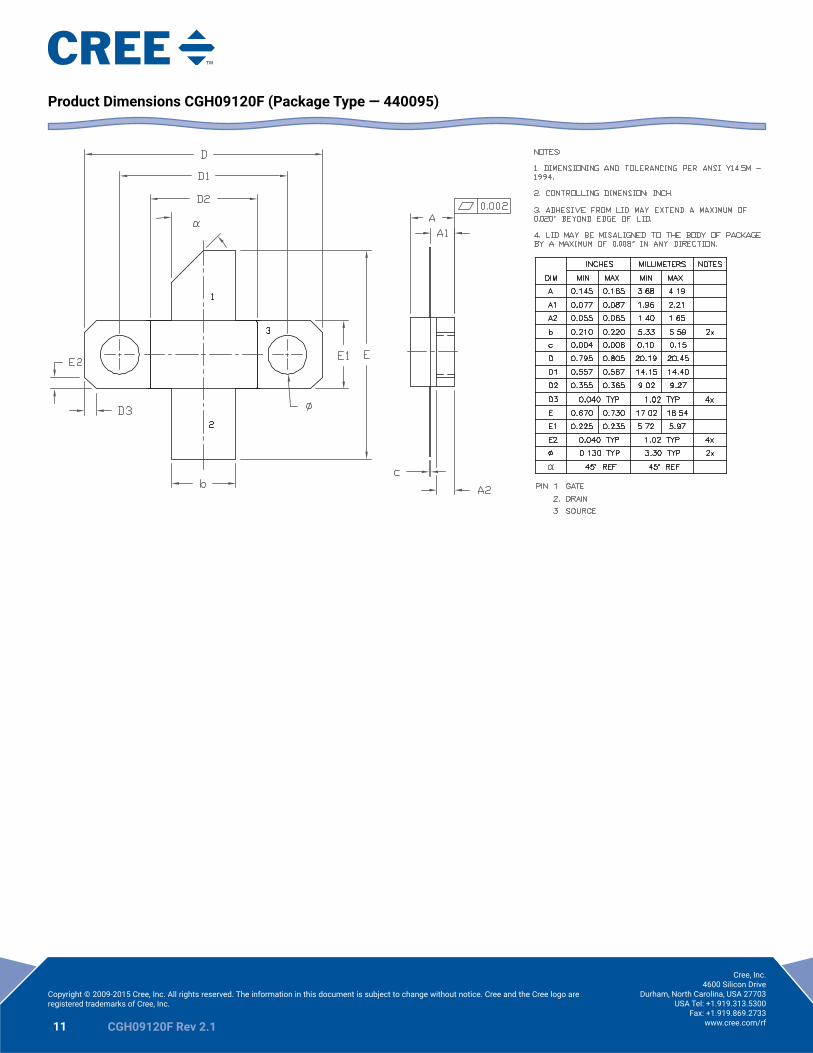
Product Dimensions CGH09120F (Package Type — 440095)

12 CGH09120F Rev 2.1
Cree, Inc.4600 Silicon Drive
Durham, North Carolina, USA 27703USA Tel: +1.919.313.5300
Fax: +1.919.869.2733www.cree.com/rf
Copyright © 2009-2015 Cree, Inc. All rights reserved. The information in this document is subject to change without notice. Cree and the Cree logo are registered trademarks of Cree, Inc.
Product Ordering Information
Order Number Description Unit of Measure Image
CGH09120F GaN HEMT Each
CGH09120F-TB Test board without GaN HEMT Each
CGH09120F-AMP Test board with GaN HEMT installed Each
13 CGH09120F Rev 2.1
Cree, Inc.4600 Silicon Drive
Durham, North Carolina, USA 27703USA Tel: +1.919.313.5300
Fax: +1.919.869.2733www.cree.com/rf
Copyright © 2009-2015 Cree, Inc. All rights reserved. The information in this document is subject to change without notice. Cree and the Cree logo are registered trademarks of Cree, Inc.
Disclaimer
Specifications are subject to change without notice. Cree, Inc. believes the information contained within this data sheet to be accurate
and reliable. However, no responsibility is assumed by Cree for any infringement of patents or other rights of third parties which may
result from its use. No license is granted by implication or otherwise under any patent or patent rights of Cree. Cree makes no warranty,
representation or guarantee regarding the suitability of its products for any particular purpose. “Typical” parameters are the average
values expected by Cree in large quantities and are provided for information purposes only. These values can and do vary in different
applications and actual performance can vary over time. All operating parameters should be validated by customer’s technical experts
for each application. Cree products are not designed, intended or authorized for use as components in applications intended for surgical
implant into the body or to support or sustain life, in applications in which the failure of the Cree product could result in personal injury or
death or in applications for planning, construction, maintenance or direct operation of a nuclear facility.
For more information, please contact:
Cree, Inc.4600 Silicon DriveDurham, North Carolina, USA 27703www.cree.com/RF
Sarah MillerMarketingCree, RF Components1.919.407.5302
Ryan BakerMarketing & SalesCree, RF Components1.919.407.7816
Tom DekkerSales DirectorCree, RF Components1.919.407.5639