Embed Size (px)
Citation preview
Ch6 DC-DC Converters6-1 Linear voltage regulators Fig. 6.1
Adjusting base current,
SLLO VRIV ~0
=> linear DC-DC converter or linear regulator The transistor operates in the linear region.
Low efficiency happen under lower output voltage.=> improved by switching converter.
6-2 A basic switching converter. Fig. 6.2
The transistor operates as an electronic switch and in saturation state.
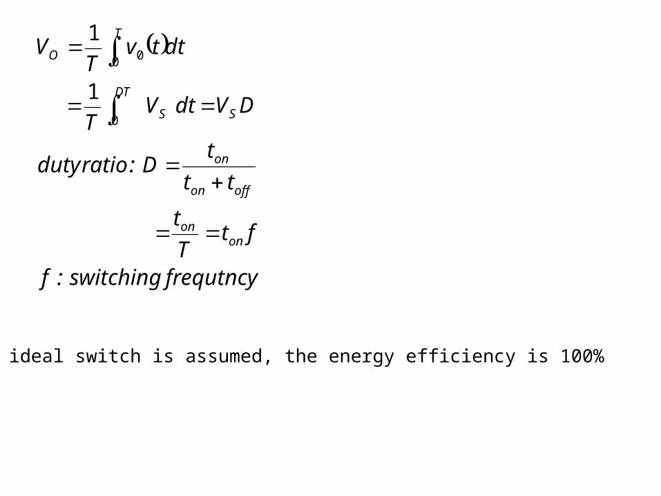
frequtncyswitching:f
ftT
t
tt
tD:ratioduty
DVdtVT
dttvT
V
onon
offon
on
S
DT
S
T
O
0
0 0
1
1
If the ideal switch is assumed, the energy efficiency is 100%
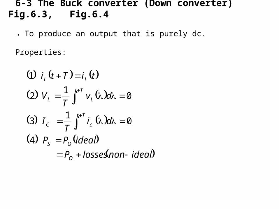
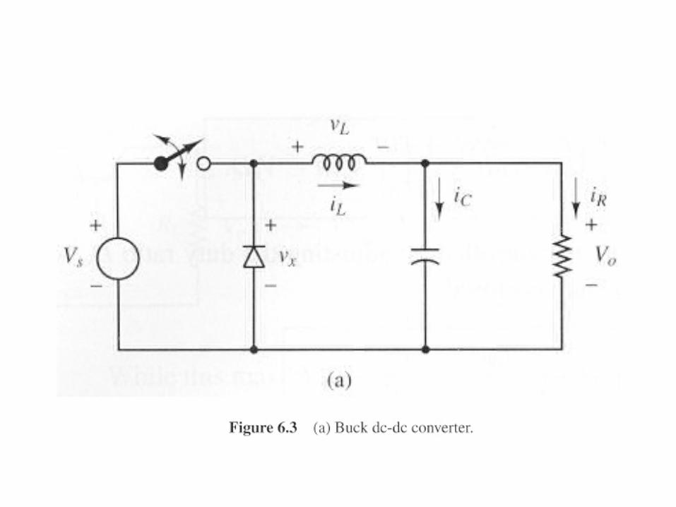
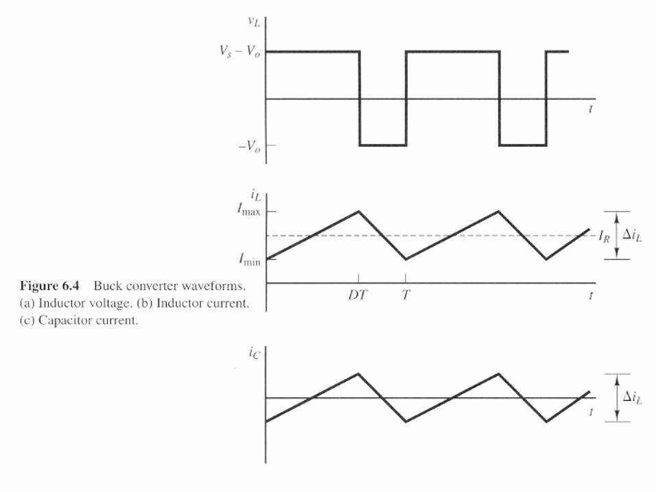
6-3 The Buck converter (Down converter) Fig.6.3, Fig.6.4
→ To produce an output that is purely dc.
Properties:
idealnonlossesP
idealPP
diT
I
dvT
V
tiTti
O
OS
Tt
t cC
Tt
t LL
LL
4
01
3
01
2
1
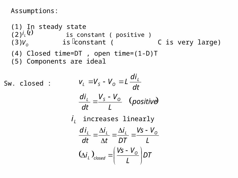
Assumptions:
(1) In steady state(2) is constant ( positive ) tiL
OV(3) is constant ( C is very large)
(4) Closed time=DT , open time=(1-D)T(5) Components are ideal
Sw. closed :
positiveL
VV
dt
iddt
idLVVv
OSL
LOSL
Li increases linearly
DTL
VVsi
L
VVs
DT
i
t
i
dt
id
OclosedL
OLLL
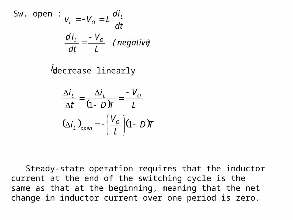
Sw. open :
)negative(L
V
dt
iddt
idLVv
OL
LOL
Li decrease linearly
TDL
Vi
L
V
TD
i
t
i
OopenL
OLL
1
1
Steady-state operation requires that the inductor current at the end of the switching cycle is the same as that at the beginning, meaning that the net change in inductor current over one period is zero.
closedLi openLi = 0
SSO
OO
VDVV
TDL
VDT
L
VVs
01
Since the average inductor voltage is zero for periodic operation
DVVT
TDVDTVVV
SO
OOSL
01
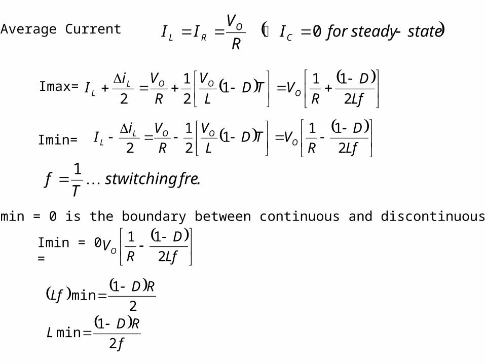
Average Current statesteadyforIR
VII C
ORL 0
Imax=
Lf
D
RVTD
L
V
R
ViI O
OOLL 2
111
2
1
2
Imin=
Lf
D
RVTD
L
V
R
ViI O
OOLL 2
111
2
1
2
.frestwitchingT
f 1
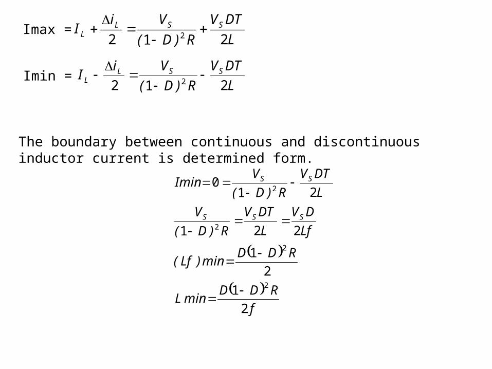
Since Imin = 0 is the boundary between continuous and discontinuous
Imin = 0 =
Lf
D
RVO 2
11
f
RDL
RDLf
2
1min
2
1min
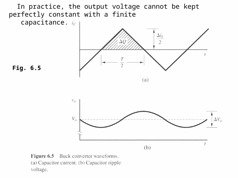
In practice, the output voltage cannot be kept perfectly constant with a finite capacitance.
Fig. 6.5
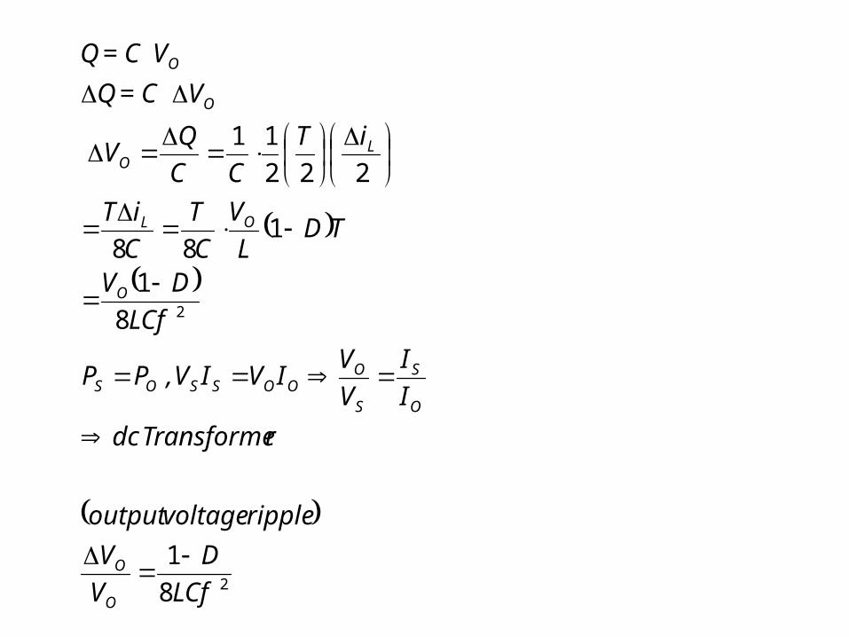
2
2
8
1
8
1
188
222
11
LCf
D
V
V
ripplevoltageoutput
rTransformedc
I
I
V
VIVIV,PP
LCf
DV
TDL
V
C
T
C
iT
iT
CC
QV
V C = Q
V C = Q
O
O
O
S
S
OOOSSOS
O
OL
LO
O
O
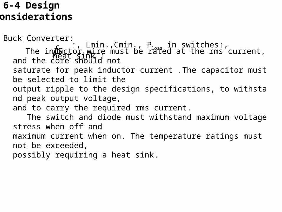
6-4 Design considerations
Buck Converter:
fs ↑, Lmin↓,Cmin↓, Ploss in switches↑, heat sink ↑
The inductor wire must be rated at the rms current, and the core should not saturate for peak inductor current .The capacitor must be selected to limit the output ripple to the design specifications, to withstand peak output voltage, and to carry the required rms current. The switch and diode must withstand maximum voltage stress when off and maximum current when on. The temperature ratings must not be exceeded, possibly requiring a heat sink.
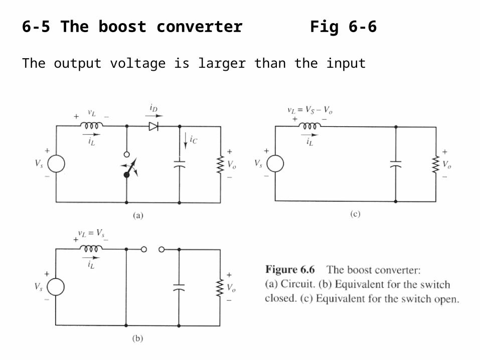
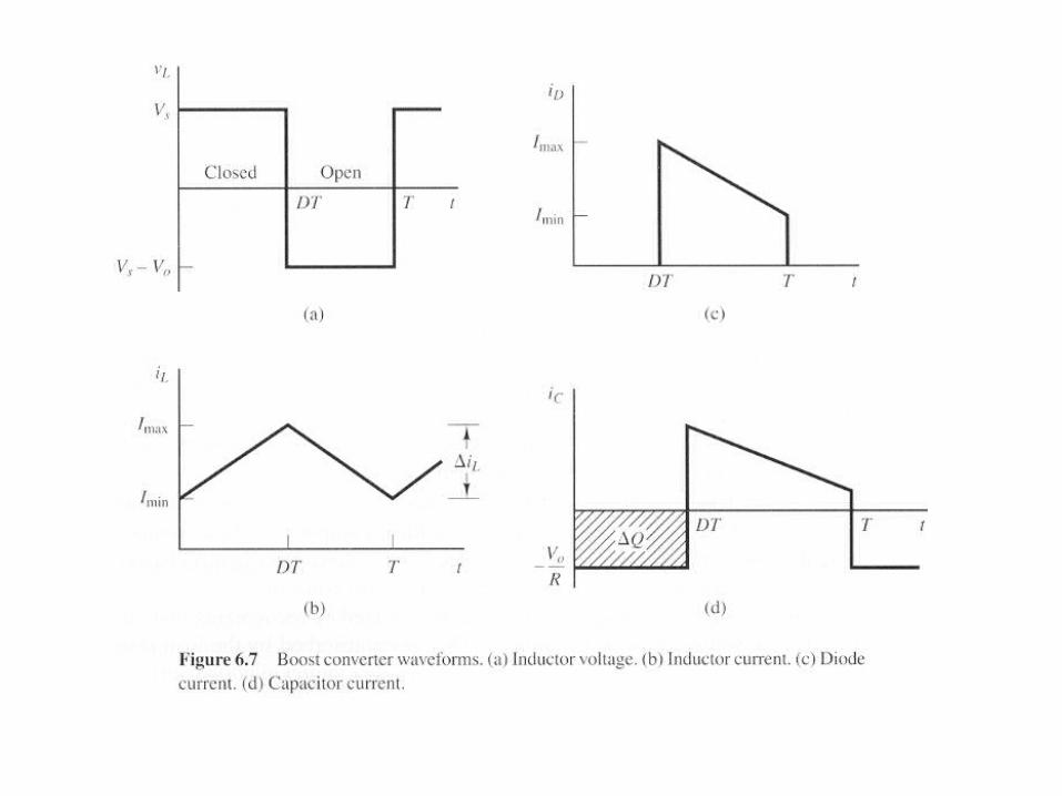
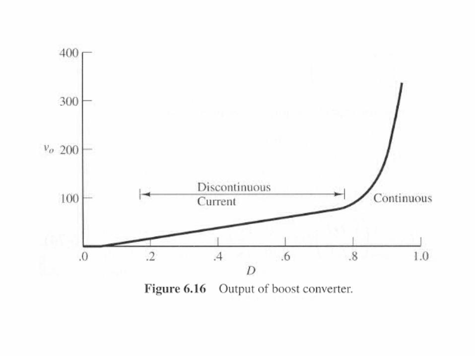
6-5 The boost converter Fig 6-6
The output voltage is larger than the input
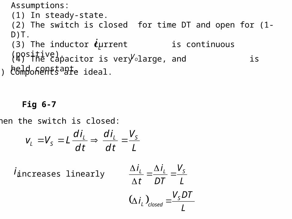
Assumptions: (1) In steady-state.(2) The switch is closed for time DT and open for (1-D)T.(3) The inductor current is continuous (positive).Li
OV
(4) The capacitor is very large, and is held constant.
(5) Components are ideal.
Fig 6-7
When the switch is closed:
L
V
td
id
td
idLVv SLL
SL
Li increases linearly
L
DTVi
L
V
DT
i
t
i
SclosedL
SLL
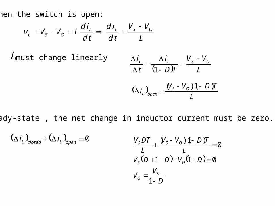
When the switch is open:
L
VV
td
id
td
idLVVv OSLL
OSL
Li must change linearly
L
VV
TD
i
t
i OSLL
1
L
TDVVi OS
openL
)1)((
For steady-state , the net change in inductor current must be zero.
0 openLclosedL ii
D
VV
DVDDVL
TDVV
L
DTV
SO
OS
OSS
1
011
0)1)((
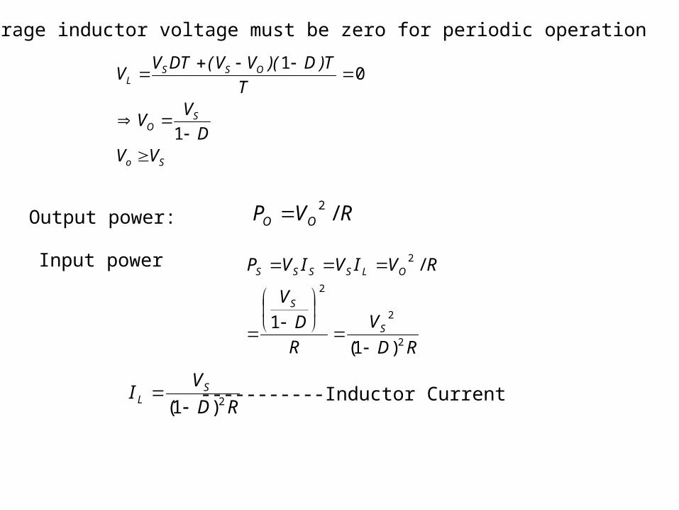
The average inductor voltage must be zero for periodic operation
So
SO
OSSL
VVD
VV
T
T)D)(VV(DTVV
1
01
Output power: RVP OO /2
Input power
RD
V
R
D
V
RVIVIVP
S
S
OLSSSS
2
2
2
2
)1(
1
/
RD
VI S
L 2)1( -----------Inductor Current
Imax = L
DTV
R)D(
ViI SSL
L 212 2
Imin = L
DTV
R)D(
ViI SSL
L 212 2
The boundary between continuous and discontinuous inductor current is determined form.
f
RDDminL
RDDmin)Lf(
Lf
DV
L
DTV
R)D(
V
L
DTV
R)D(
V Imin
SSS
SS
2
1
2
1
221
210
2
2
2
2
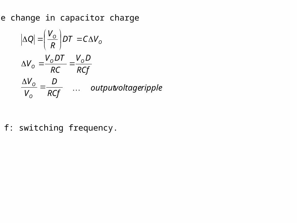
The change in capacitor charge
ripplevoltageoutputRCf
D
V
VRCf
DV
RC
DTVV
VCDTR
VQ
O
O
OOO
OO
f: switching frequency.
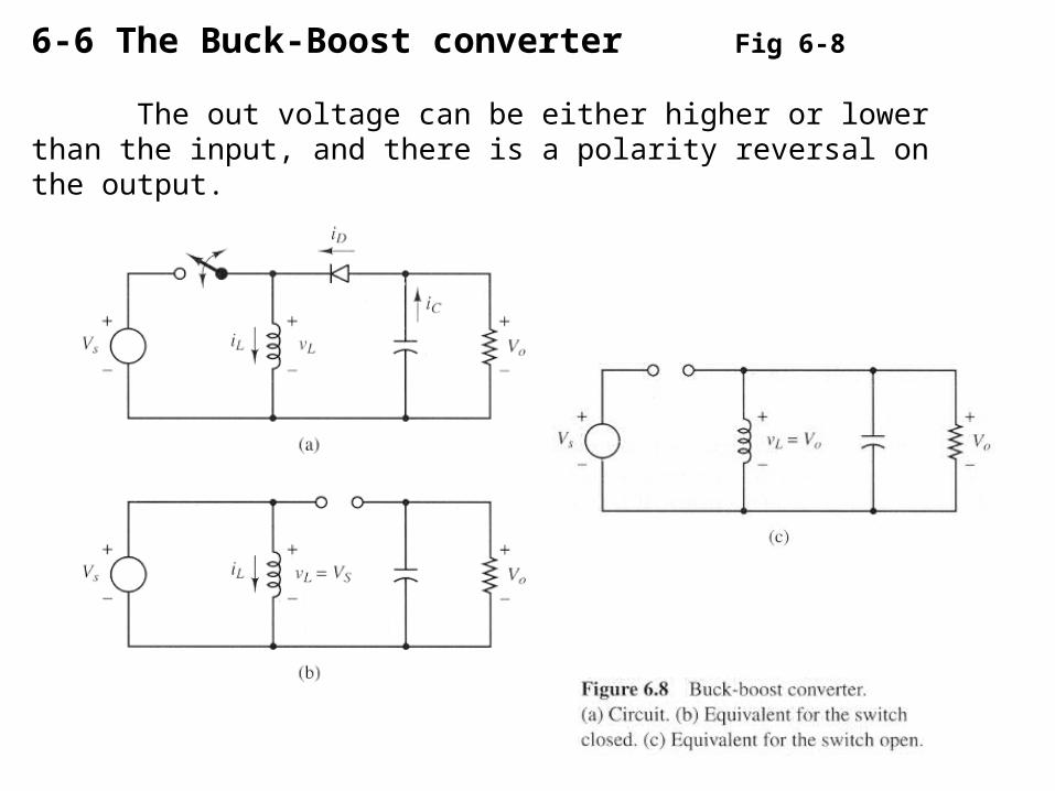
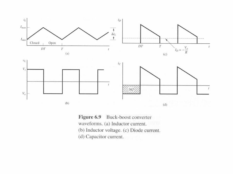
6-6 The Buck-Boost converter Fig 6-8
The out voltage can be either higher or lower than the input, and there is a polarity reversal on the output.
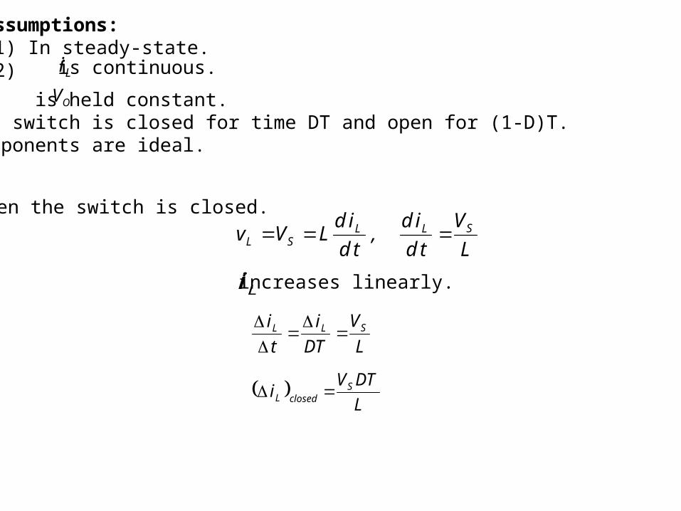
Assumptions: (1) In steady-state.(2) Li is continuous.
OV(3) is held constant.(4) The switch is closed for time DT and open for (1-D)T.(5) Components are ideal.
When the switch is closed.
L
V
td
id,
td
idLVv SLL
SL
Li increases linearly.
L
V
DT
i
t
i SLL
L
DTVi S
closedL
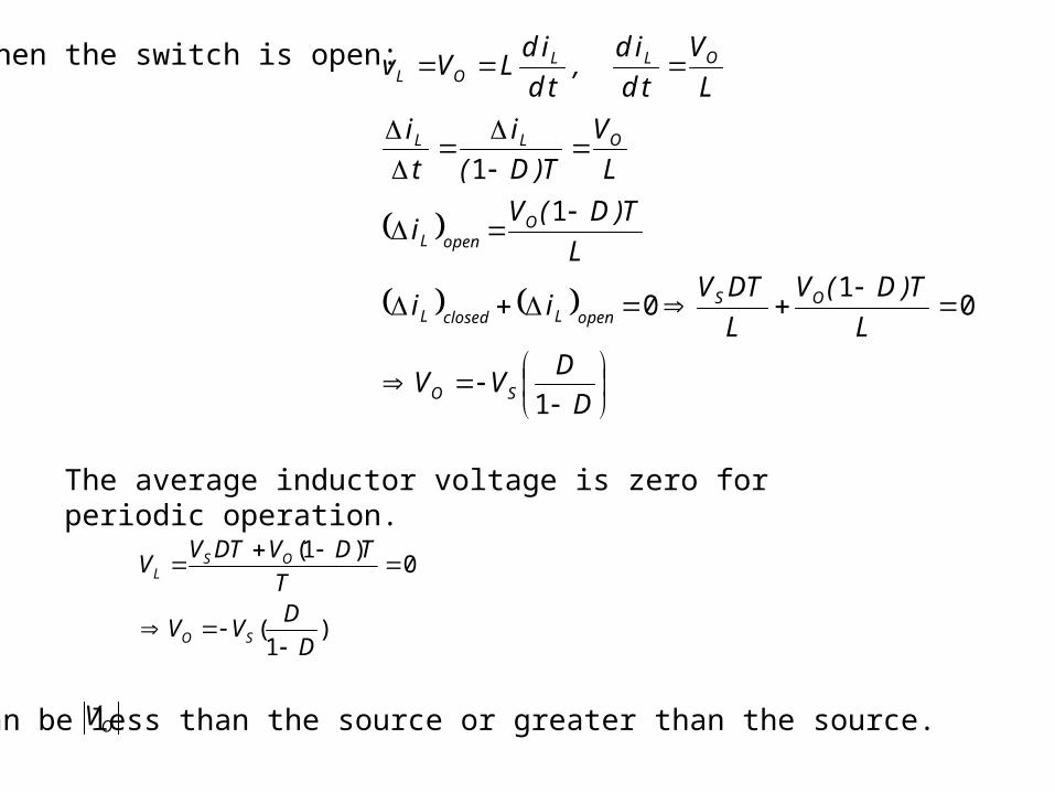
When the switch is open:
D
DVV
L
T)D(V
L
DTVii
L
T)D(Vi
L
V
T)D(
i
t
i
L
V
td
id,
td
idLVv
SO
OSopenLclosedL
OopenL
OLL
OLLOL
1
01
0
1
1
The average inductor voltage is zero for periodic operation.
)1
(
0)1(
D
DVV
T
TDVDTVV
SO
OSL
OV can be less than the source or greater than the source.
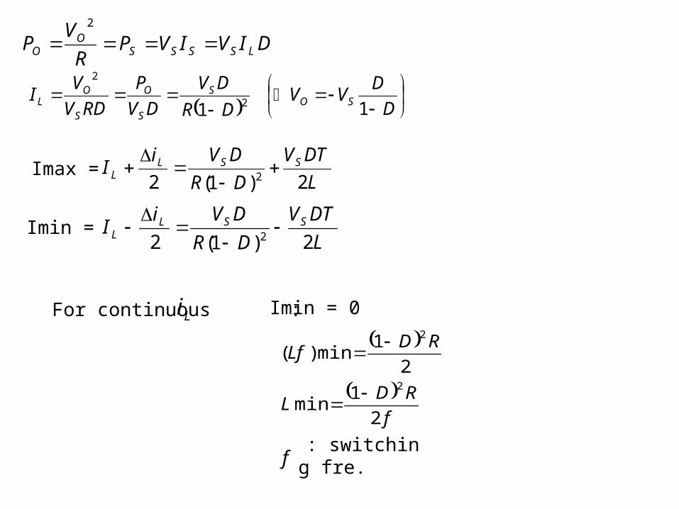
DIVIVPR
VP LSSSS
OO
2
D
DVV
DR
DV
DV
P
RDV
VI SO
S
S
O
S
OL 11 2
2
Imax = L
DTV
DR
DViI SSL
L 2)1(2 2
Imin = L
DTV
DR
DViI SSL
L 2)1(2 2
For continuous :Li Imin = 0
f
RDL
RDLf
2
1min
2
1min)(
2
2
f : switching fre.
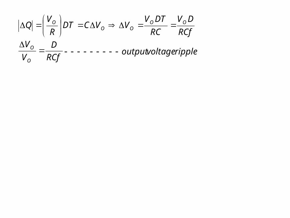
ripplevoltageoutputRCf
D
V
V
RCf
DV
RC
DTVVVCDT
R
VQ
O
O
OOOO
O
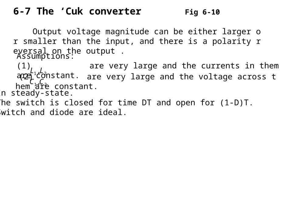
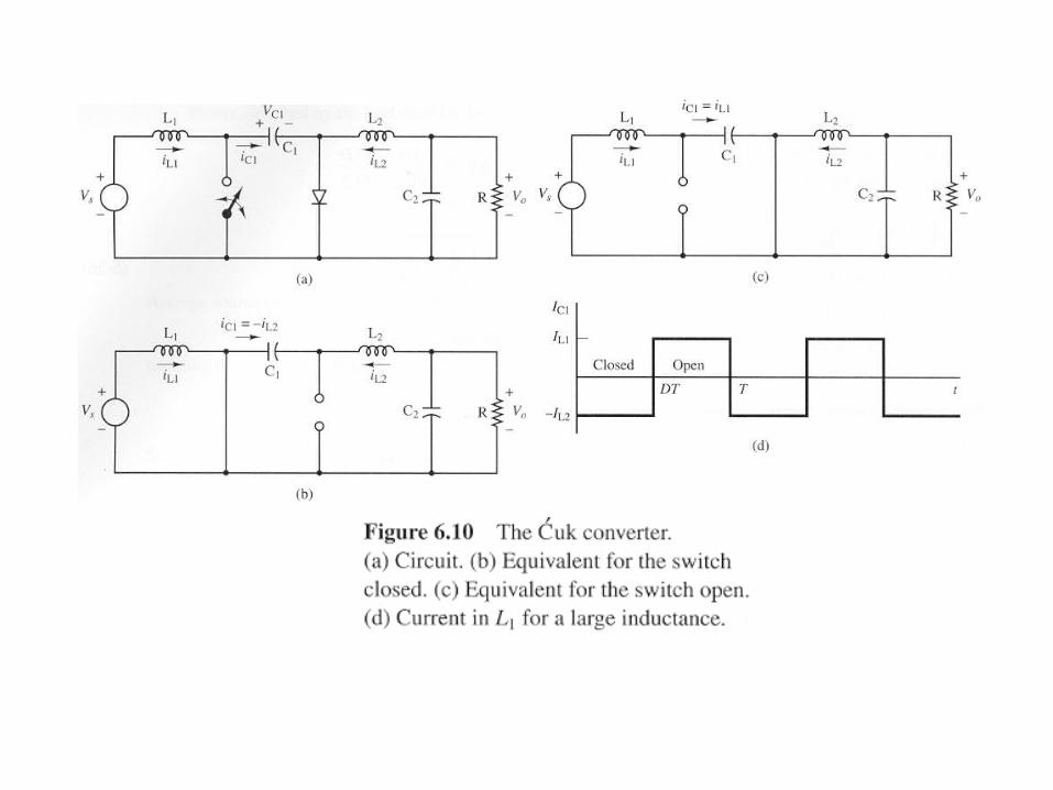
6-7 The ‘Cuk converter Fig 6-10
Output voltage magnitude can be either larger or smaller than the input, and there is a polarity reversal on the output .
Assumptions: (1) are very large and the currents in them are constant.21 , LL
(2) are very large and the voltage across them are constant.21 ,CC
(3) In steady-state.(4) The switch is closed for time DT and open for (1-D)T.(5) Switch and diode are ideal.
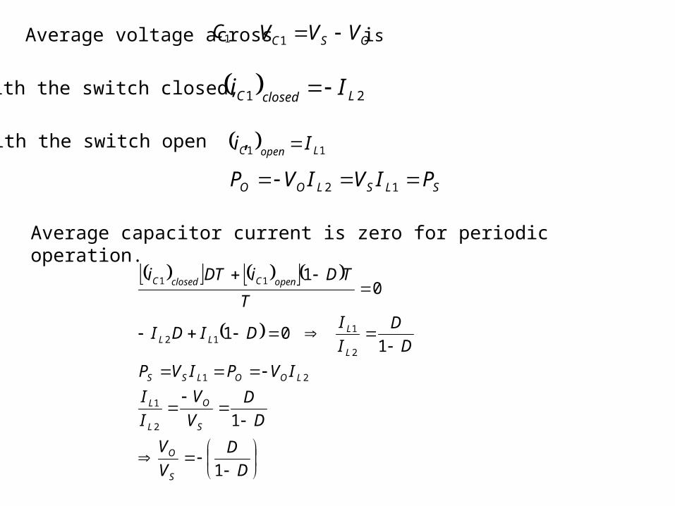
Average voltage across is1C
OSC VVV 1
With the switch closed, 21 LclosedC Ii
With the switch open , 11 LopenC Ii
SLSLOO PIVIVP 12
Average capacitor current is zero for periodic operation.
D
D
V
V
D
D
V
V
I
I
IVPIVP
D
D
I
IDIDI
T
TDiDTi
S
O
S
O
L
L
LOOLSS
L
LLL
openCclosedC
1
1
101
01
2
1
21
2
112
11
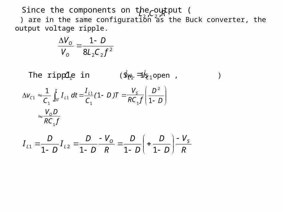
Since the components on the output ( ) are in the same configuration as the Buck converter, the output voltage ripple.
RCL ,, 22
2228
1
fCL
D
V
V
O
O
The ripple in (Sw. is open , )1C
11 CL ii
fRCDV
D
DfRC
VT)D(
C
IdtI
Cv
O
SLT
DT LC
1
2
11
11
11 1
11
R
V
D
D
D
D
R
V
D
DI
D
DI SO
LL
1111 21
When Sw. is closed,
fL
DV
L
DTVi
xd
idLVVVVv
fL
DV
L
DTVi
L
V
DT
i,
td
idLVv
SSL
LSOSOL
SSL
SLLsL
222
222
111
1
1111
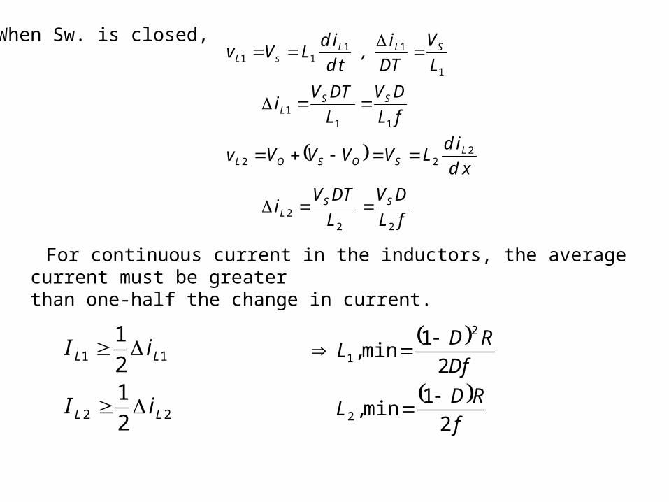
For continuous current in the inductors, the average current must be greater than one-half the change in current.
22
11
2
12
1
LL
LL
iI
iI
f
RDL
Df
RDL
2
1min,
2
1min,
2
2
1
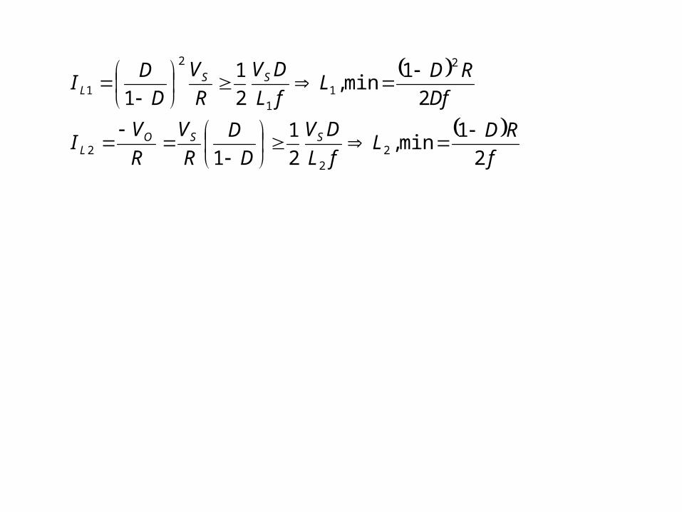
f
RDL
fL
DV
D
D
R
V
R
VI
Df
RDL
fL
DV
R
V
D
DI
SSOL
SSL
2
1min,
2
1
1
2
1min,
2
1
1
22
2
2
11
2
1
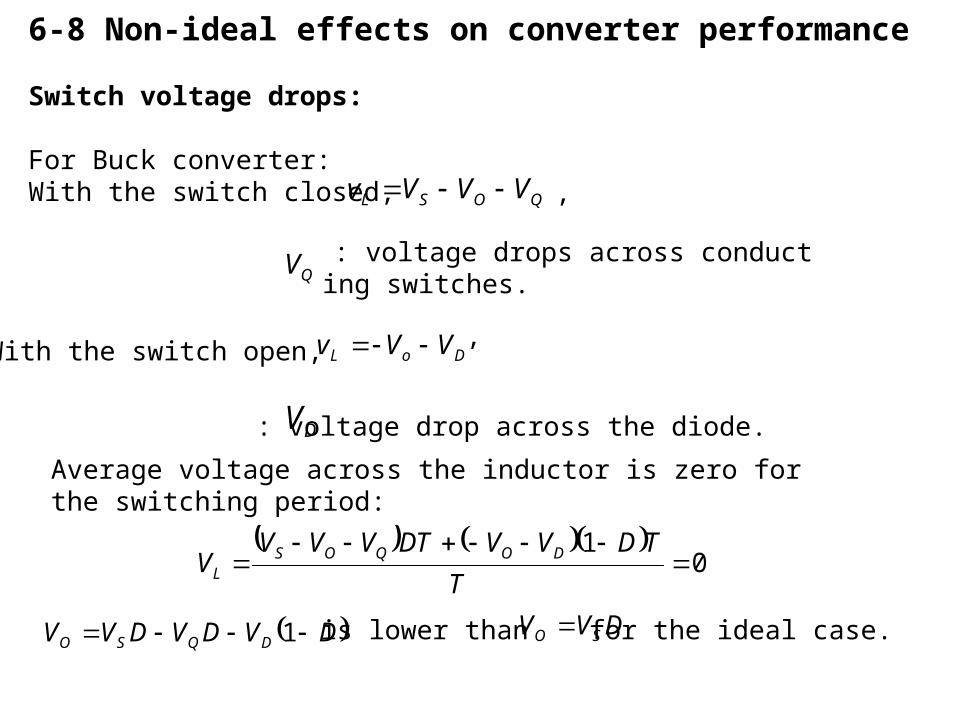
6-8 Non-ideal effects on converter performance
Switch voltage drops:
For Buck converter:With the switch closed, QOSL VVVv ,
QV : voltage drops across conducting switches.
With the switch open, DoL VVv ,
DV : voltage drop across the diode.
Average voltage across the inductor is zero for the switching period:
0
1
T
TDVVDTVVVV DOQOS
L
DVDVDVV DQSO 1 is lower than DVV SO for the ideal case.
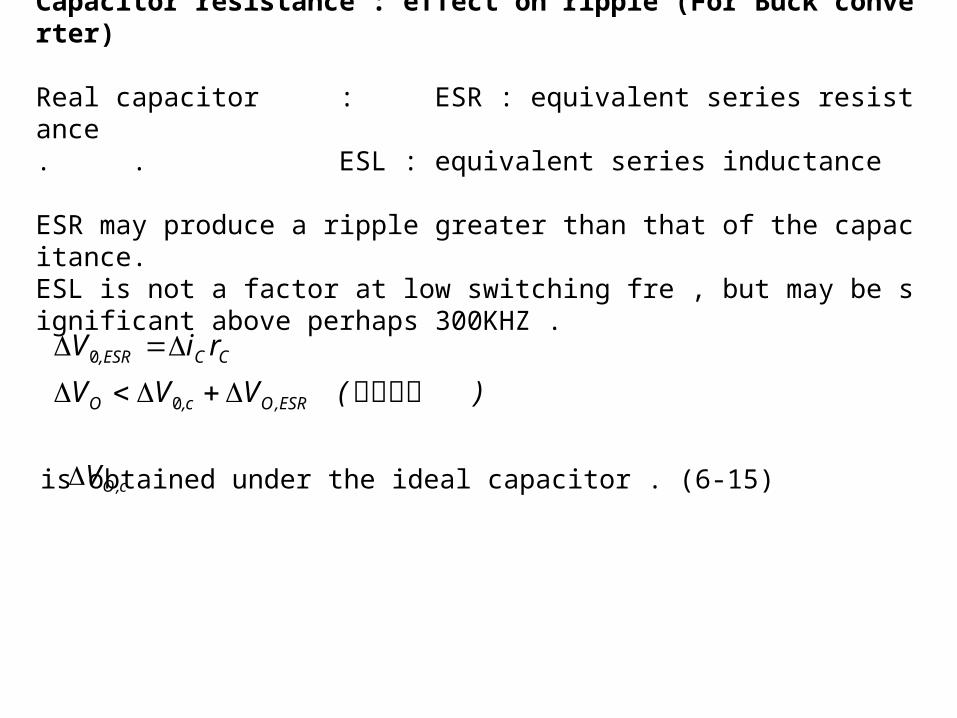
Capacitor resistance : effect on ripple (For Buck converter)
Real capacitor : ESR : equivalent series resistance. . ESL : equivalent series inductance
ESR may produce a ripple greater than that of the capacitance.ESL is not a factor at low switching fre , but may be significant above perhaps 300KHZ .
)(VVV
riV
ESR,Oc,O
CCESR,
最差情況0
0
c,OV is obtained under the ideal capacitor . (6-15)
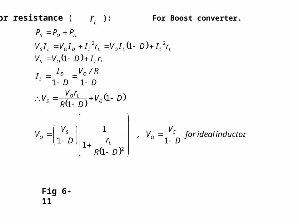
Inductor resistance ( ): For Boost converter.Lr
.inductoridealforD
VV,
DR
rD
VV
DVDR
rVV
D
R/V
D
II
rIDVV
rIDIVrIIVIV
PPP
SO
L
SO
OLO
S
ODL
LLOS
LLLOLLDOLS
rLOS
1
11
1
1
11
11
1
1
2
22
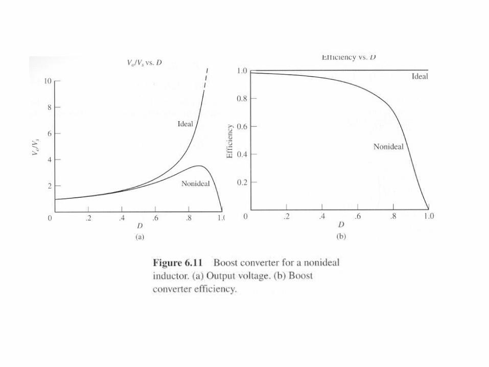
Fig 6-11
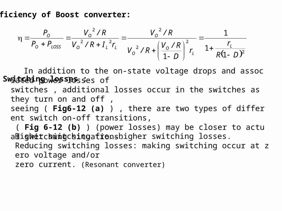
Efficiency of Boost converter:
2
22
2
22
2
11
1
1 DR
rr
D
R/VR/V
R/V
rIR/V
R/V
PP
P
L
LO
O
O
LLO
O
LOSSO
O
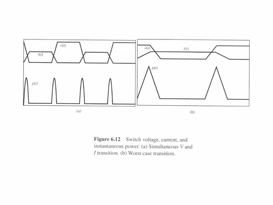
Switching losses : In addition to the on-state voltage drops and associated power losses of switches , additional losses occur in the switches as they turn on and off , seeing ( Fig6-12 (a) ) , there are two types of different switch on-off transitions, ( Fig 6-12 (b) ) (power losses) may be closer to actual switching situations.
Higher switching fre.→higher switching losses.Reducing switching losses: making switching occur at zero voltage and/or zero current. (Resonant converter)
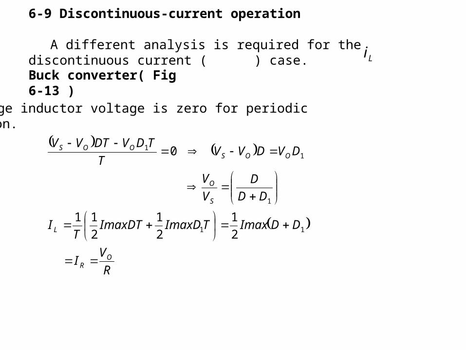
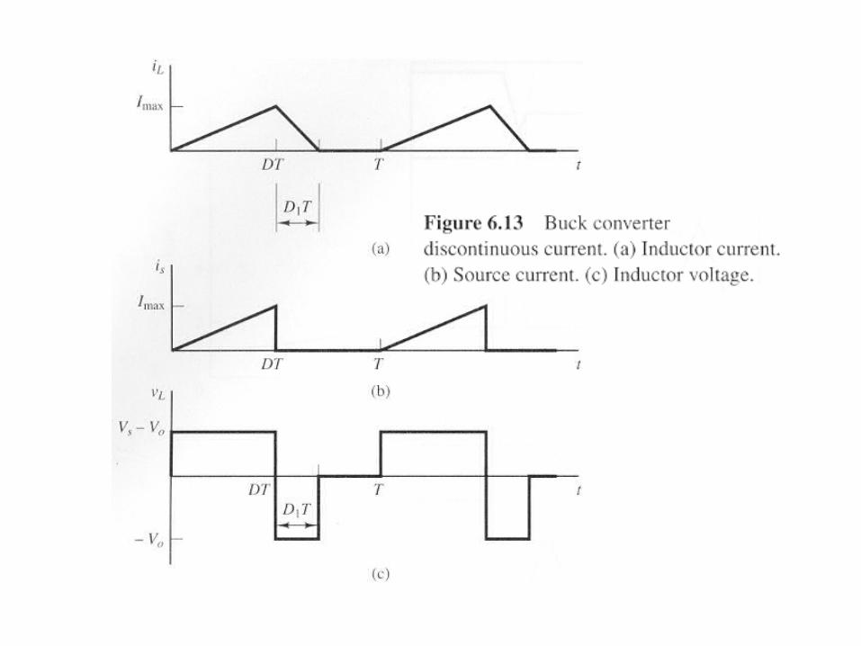
6-9 Discontinuous-current operation
A different analysis is required for the discontinuous current ( ) case.Li
Buck converter( Fig 6-13 )
Average inductor voltage is zero for periodic operation.
R
VI
DDaxImTaxDImaxDTImT
I
DD
D
V
V
DVDVVT
TDVDTVV
OR
L
S
O
OOSOOS
11
1
11
2
1
2
1
2
11
0
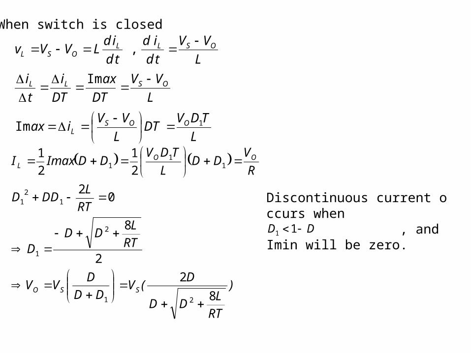
When switch is closed
L
TDVDT
L
VViax
L
VV
DT
ax
DT
i
t
i
L
VV
td
id
td
idLVVv
OOSL
OSLL
OSLLOSL
1Im
Im
,
)
RT
LDD
D(V
DD
DVV
RT
LDD
D
RT
LDDD
R
VDD
L
TDVDDaxImI
SSO
OOL
8
2
2
8
02
2
1
2
1
21
2
1
12
1
11
1
Discontinuous current occurs when , and Imin will be zero.DD 11
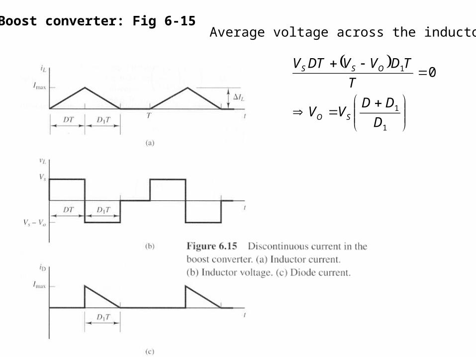
Boost converter: Fig 6-15Average voltage across the inductor:
1
1
1 0
D
DDVV
T
TDVVDTV
SO
OSS
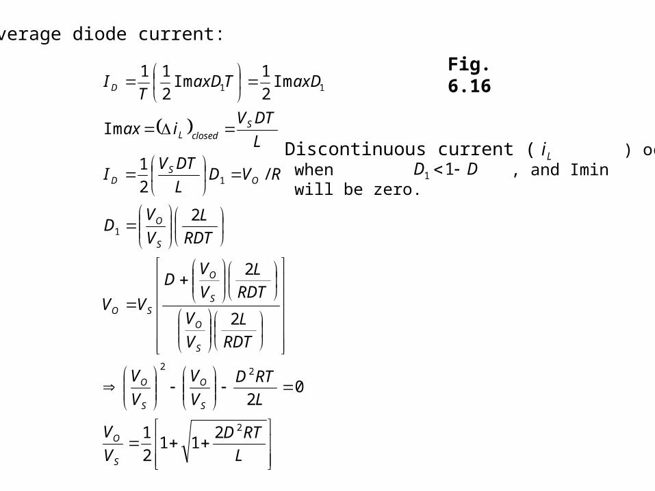
Average diode current:
L
RTD
V
V
L
RTD
V
V
V
V
RDT
L
V
V
RDT
L
V
VD
VV
RDT
L
V
VD
RVDL
DTVI
L
DTViax
axDTaxDT
I
S
O
S
O
S
O
S
O
S
O
SO
S
O
OS
D
SclosedL
D
2
22
1
1
11
211
2
1
02
2
2
2
/2
1
Im
Im2
1Im
2
11 Fig. 6.16
Discontinuous current ( ) occurs when , and Imin will be zero.
LiDD 11


![The Physics of the DC Motor - catalogimages.wiley.com€¦ · 1. The Physics of the DC Motor Example A Linear DC Machine [19] Consider the simple linear DC machine in Figure 1.3 where](https://img.pdfslide.net/doc/110x75/5f670fcb5bbe8f48f66a1015/the-physics-of-the-dc-motor-1-the-physics-of-the-dc-motor-example-a-linear-dc.jpg)


![dc ch6 [호환 모드]yu.ac.kr/~shkwon/lectures/dc/dc_ch6.pdf · *Synchronous sequential circuit(동기식순차회로) is one in which its behavior is determined by the values of](https://img.pdfslide.net/doc/110x75/5e5d829292b6c26d49247b28/dc-ch6-eeoeyuackrshkwonlecturesdcdcch6pdf-synchronous-sequential.jpg)


![[Note] Chapter 1 - Linear DC Power Supply](https://img.pdfslide.net/doc/110x75/553299b255034687698b4651/note-chapter-1-linear-dc-power-supply.jpg)