Embed Size (px)
Citation preview
EE141System-on-Chip Test Architectures Ch. 1 – Introduction - P. 1
Chapter 1Chapter 1
IntroductionIntroduction
EE141System-on-Chip Test Architectures Ch. 1 – Introduction - P. 2
What is this chapter about?� Review of
� Importance of Testing� Yield and Reject Rate� Reliability and System Availability
� Overview of � Boundary Scan (IEEE 1149.1 Std.)� Boundary-Scan Extension (IEEE 1149.6 Std.)� Boundary-Scan Accessible Embedded Instruments (IEEE
P1687) � Core-Based Testing (IEEE 1500 Std.)� Analog Boundary Scan (IEEE 1149.4 Std.)� Memory Testing
� Two SOC Design Examples� Brief Description of the Book
EE141System-on-Chip Test Architectures Ch. 1 – Introduction - P. 3
Introduction
� Importance of SOC Testing
�Basics of SOC Testing
�Basics of Memory Testing
�SOC Design Examples
�About This Book
EE141System-on-Chip Test Architectures Ch. 1 – Introduction - P. 4
Section 1.1Section 1.1
Importance of SOC TestingImportance of SOC Testing
EE141System-on-Chip Test Architectures Ch. 1 – Introduction - P. 5
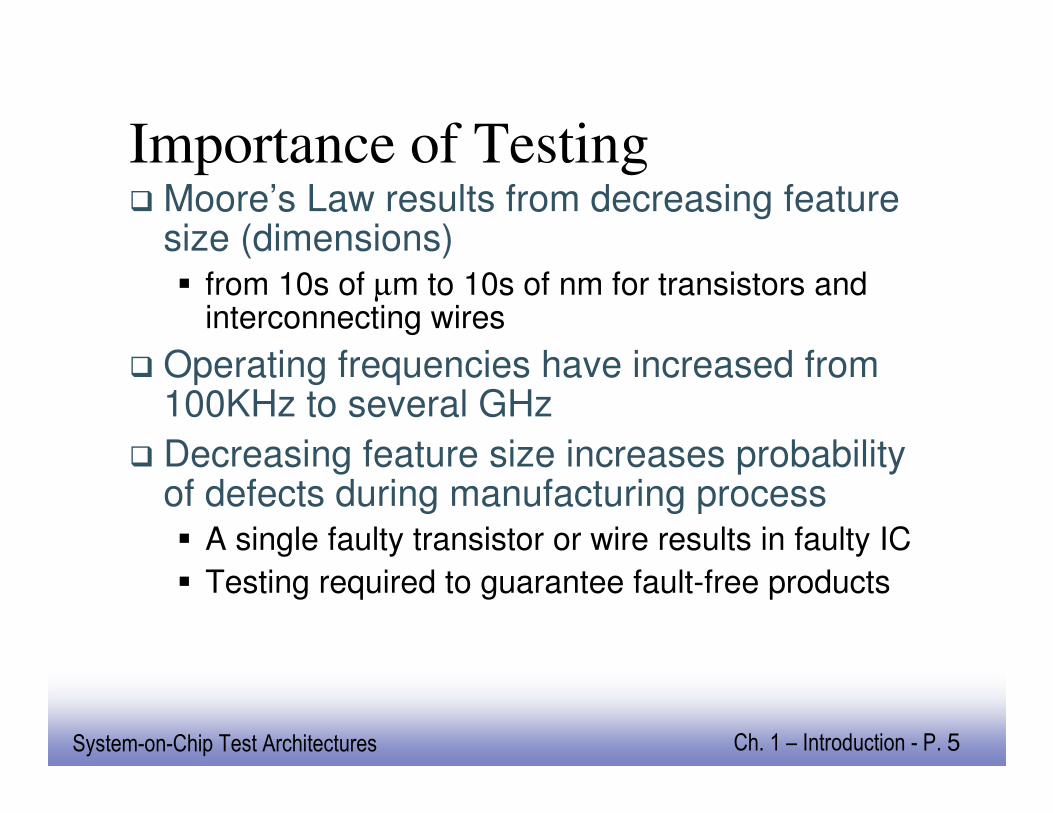
Importance of Testing� Moore’s Law results from decreasing feature
size (dimensions)� from 10s of µm to 10s of nm for transistors and
interconnecting wires
� Operating frequencies have increased from 100KHz to several GHz
� Decreasing feature size increases probability of defects during manufacturing process� A single faulty transistor or wire results in faulty IC
� Testing required to guarantee fault-free products
EE141System-on-Chip Test Architectures Ch. 1 – Introduction - P. 6
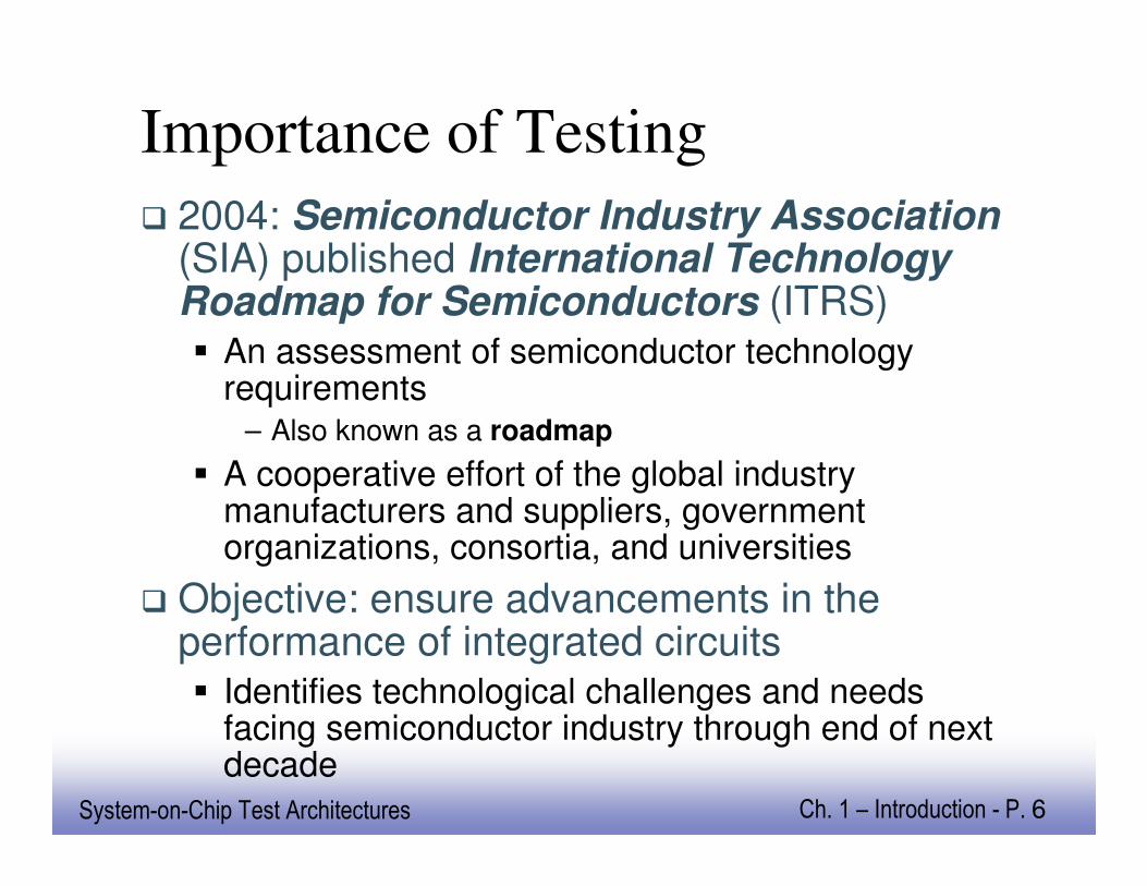
Importance of Testing
� 2004: Semiconductor Industry Association (SIA) published International Technology Roadmap for Semiconductors (ITRS)� An assessment of semiconductor technology
requirements– Also known as a roadmap
� A cooperative effort of the global industry manufacturers and suppliers, government organizations, consortia, and universities
� Objective: ensure advancements in the performance of integrated circuits� Identifies technological challenges and needs
facing semiconductor industry through end of next decade
EE141System-on-Chip Test Architectures Ch. 1 – Introduction - P. 7
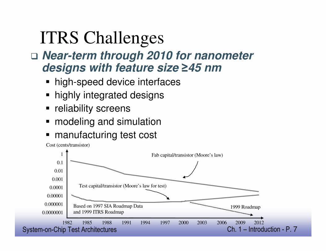
ITRS Challenges� Near-term through 2010 for nanometer
designs with feature size ≥45 nm� high-speed device interfaces
� highly integrated designs
� reliability screens
� modeling and simulation
� manufacturing test cost
1982 1985 1988 1991 1994 1997 2000 2003 2006 2009 2012
Based on 1997 SIA Roadmap Data
and 1999 ITRS Roadmap 1999 Roadmap
1
0.1
0.01
0.001
0.0001
0.00001
0.000001
0.0000001
Test capital/transistor (Moore’s law for test)
Fab capital/transistor (Moore’s law)
Cost (cents/transistor)
EE141System-on-Chip Test Architectures Ch. 1 – Introduction - P. 8
ITRS Challenges� Long-term beyond 2010 for feature size <45nm
� Device under test (DUT) to automatic test equipment (ATE) interface
� Test methodologies
� Defect analysis
� Failure analysis,
� Disruptive device technologies
� Test technology development imperative for nanometer designs� New design for testability (DFT) and design for
manufacturability (DFM) methods for digital circuits, analog circuits, MEMS, and sensors
� Means to reduce manufacturing test costs as well as enhance device reliability and yield
� Techniques to facilitate defect and failure analysis
EE141System-on-Chip Test Architectures Ch. 1 – Introduction - P. 9
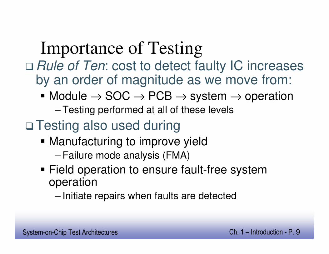
Importance of Testing�Rule of Ten: cost to detect faulty IC increases
by an order of magnitude as we move from:� Module → SOC → PCB → system → operation
– Testing performed at all of these levels
�Testing also used during� Manufacturing to improve yield
– Failure mode analysis (FMA)
� Field operation to ensure fault-free system operation
– Initiate repairs when faults are detected
EE141System-on-Chip Test Architectures Ch. 1 – Introduction - P. 10
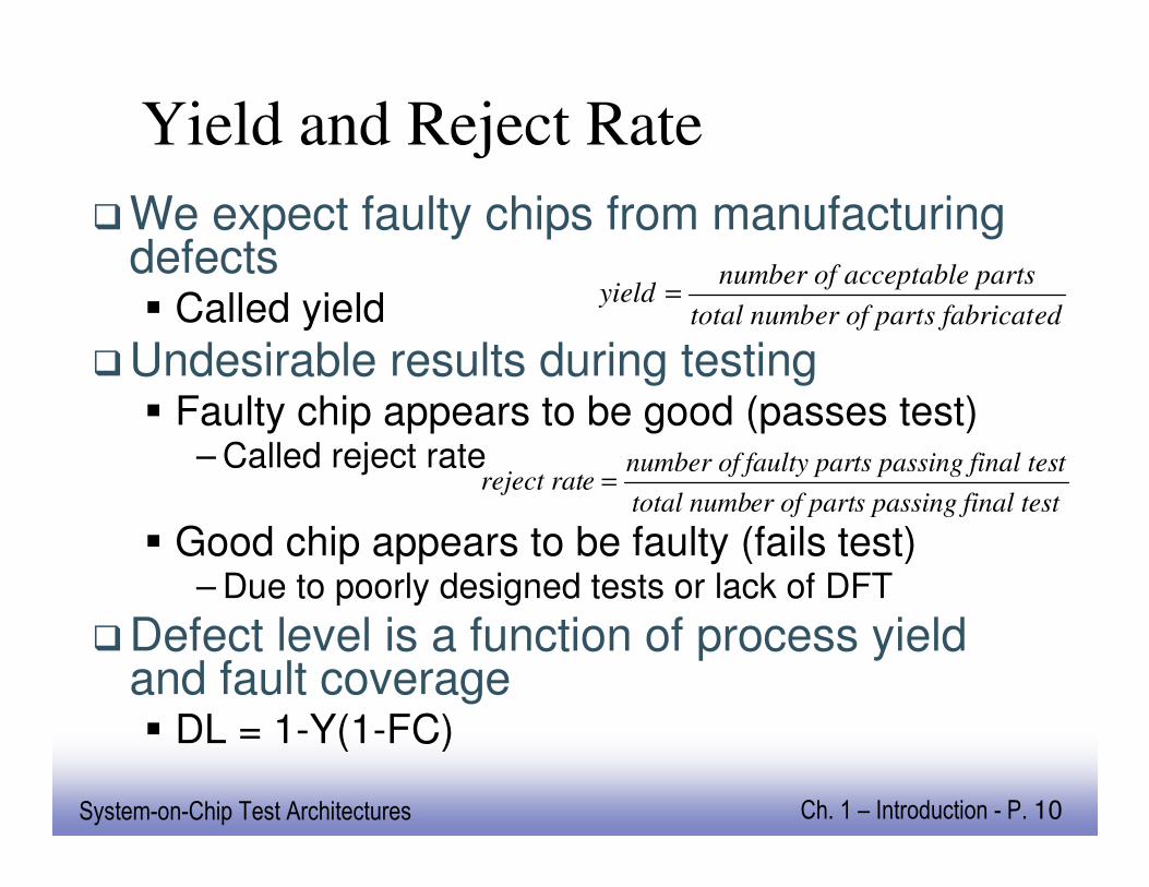
Yield and Reject Rate
�We expect faulty chips from manufacturing defects� Called yield
�Undesirable results during testing� Faulty chip appears to be good (passes test)
– Called reject rate
� Good chip appears to be faulty (fails test)– Due to poorly designed tests or lack of DFT
�Defect level is a function of process yield and fault coverage� DL = 1-Y(1-FC)
eds fabricater of parttotal numb
partsacceptablenumber of yield =
final tests passing er of parttotal numb
t final tests passingfaulty parnumber of ereject rat =
EE141System-on-Chip Test Architectures Ch. 1 – Introduction - P. 11
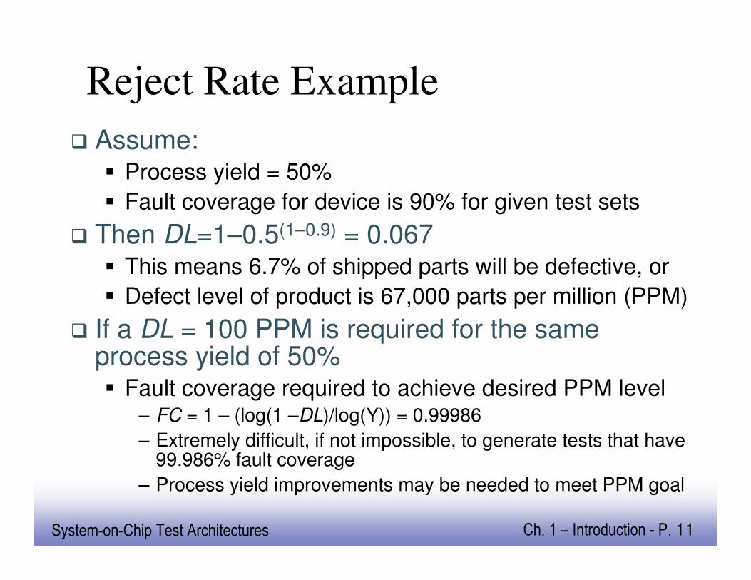
Reject Rate Example
� Assume:� Process yield = 50%
� Fault coverage for device is 90% for given test sets
� Then DL=1–0.5(1–0.9) = 0.067� This means 6.7% of shipped parts will be defective, or
� Defect level of product is 67,000 parts per million (PPM)
� If a DL = 100 PPM is required for the same process yield of 50%� Fault coverage required to achieve desired PPM level
– FC = 1 – (log(1 –DL)/log(Y)) = 0.99986
– Extremely difficult, if not impossible, to generate tests that have 99.986% fault coverage
– Process yield improvements may be needed to meet PPM goal
EE141System-on-Chip Test Architectures Ch. 1 – Introduction - P. 12
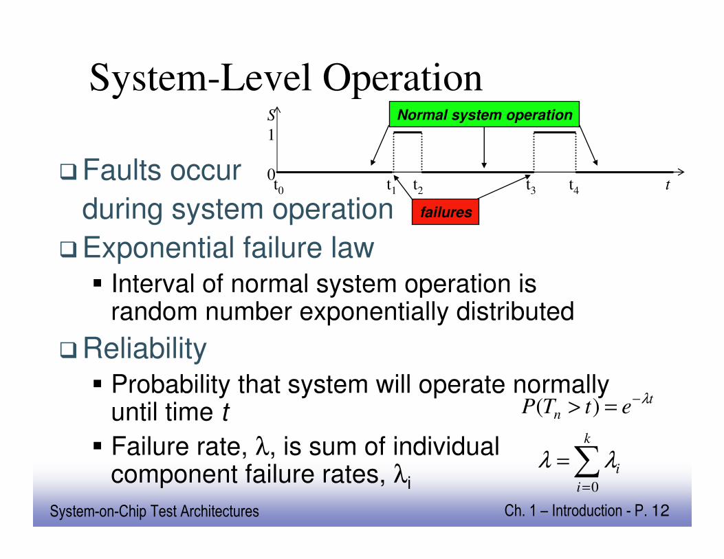
System-Level Operation
�Faults occur
during system operation
�Exponential failure law� Interval of normal system operation is
random number exponentially distributed
�Reliability� Probability that system will operate normally
until time t
� Failure rate, λ, is sum of individual component failure rates, λi
tn etTP
λ−=> )(
∑=
=k
i
i
0
λλ
t0 t1 t2 t3 t4 t
S
1
0
failures
Normal system operation
EE141System-on-Chip Test Architectures Ch. 1 – Introduction - P. 13
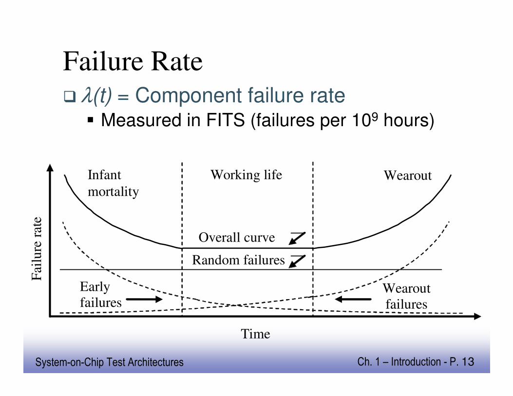
Failure Rate� λ(t) = Component failure rate
� Measured in FITS (failures per 109 hours)
Early
failures Wearout
failures
Random failures
Infant
mortality
Working life Wearout
Time
Fai
lure
rat
e
Overall curve
EE141System-on-Chip Test Architectures Ch. 1 – Introduction - P. 14
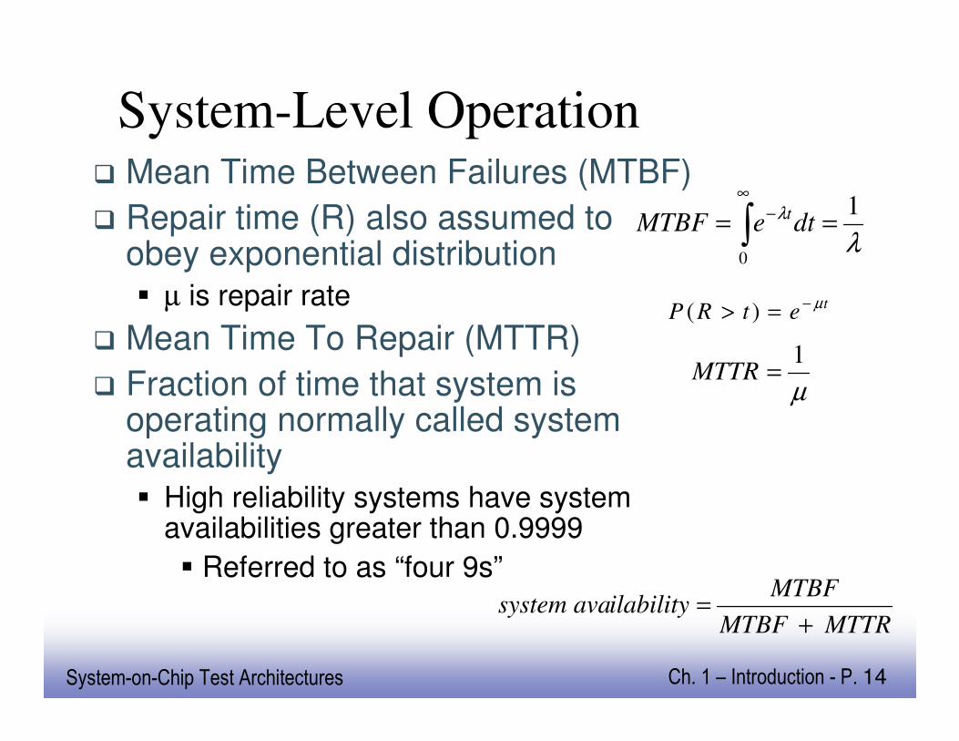
System-Level Operation� Mean Time Between Failures (MTBF)
� Repair time (R) also assumed to obey exponential distribution� µ is repair rate
� Mean Time To Repair (MTTR)
� Fraction of time that system is operating normally called system availability� High reliability systems have system
availabilities greater than 0.9999
� Referred to as “four 9s”
λλ 1
0
== ∫∞
−dteMTBF
t
µ
1=MTTR
MTTRMTBF
MTBFilabilitysystem ava
+=
tetRP
µ−=> )(
EE141System-on-Chip Test Architectures Ch. 1 – Introduction - P. 15
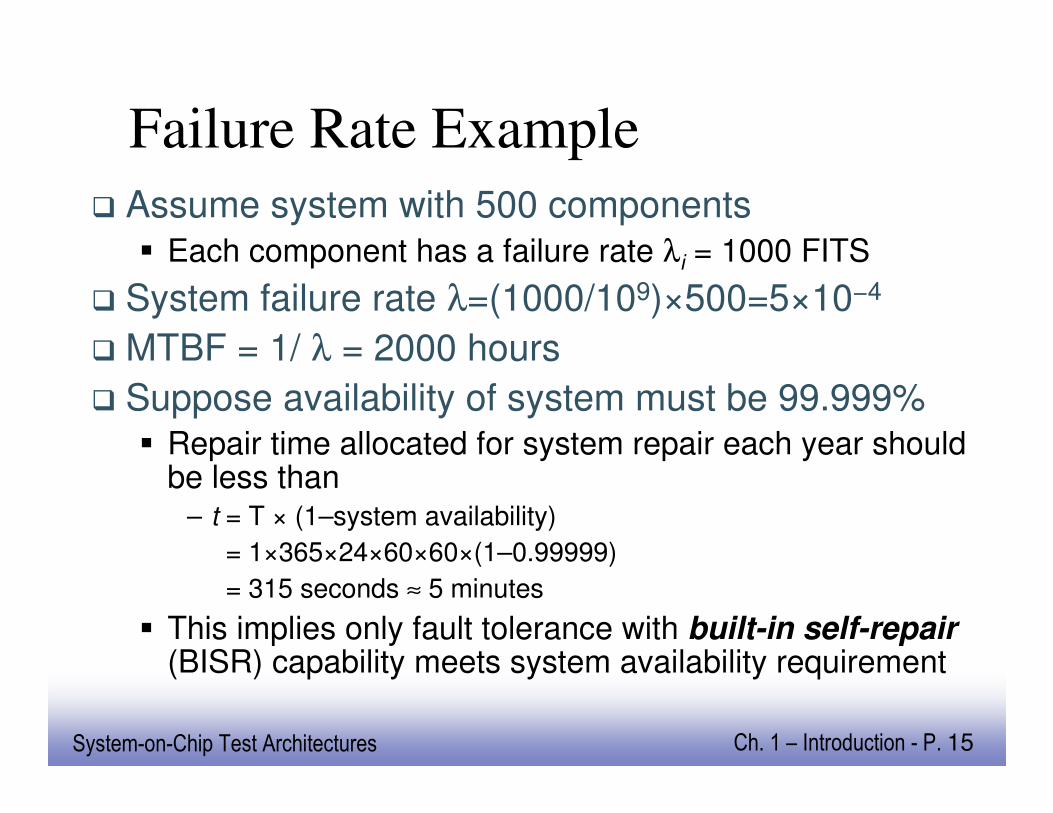
Failure Rate Example
� Assume system with 500 components� Each component has a failure rate λi = 1000 FITS
� System failure rate λ=(1000/109)×500=5×10−4
� MTBF = 1/ λ = 2000 hours
� Suppose availability of system must be 99.999%� Repair time allocated for system repair each year should
be less than– t = T × (1–system availability)
= 1×365×24×60×60×(1–0.99999)
= 315 seconds ≈ 5 minutes
� This implies only fault tolerance with built-in self-repair (BISR) capability meets system availability requirement
EE141System-on-Chip Test Architectures Ch. 1 – Introduction - P. 16
Design for Testability� Scan Design
� Replace all selected storage elements with scan cells
� Connect scan cells into multiple shift registers (scan chains)
� Become inefficient to test deep submicron or nanometer VLSI
� Logic Built-In Self-Test (BIST)� Combine with scan approach at the design stage
� Generate test patterns and analyze the output response
� Crucial for safety-critical and mission-critical applications
EE141System-on-Chip Test Architectures Ch. 1 – Introduction - P. 17
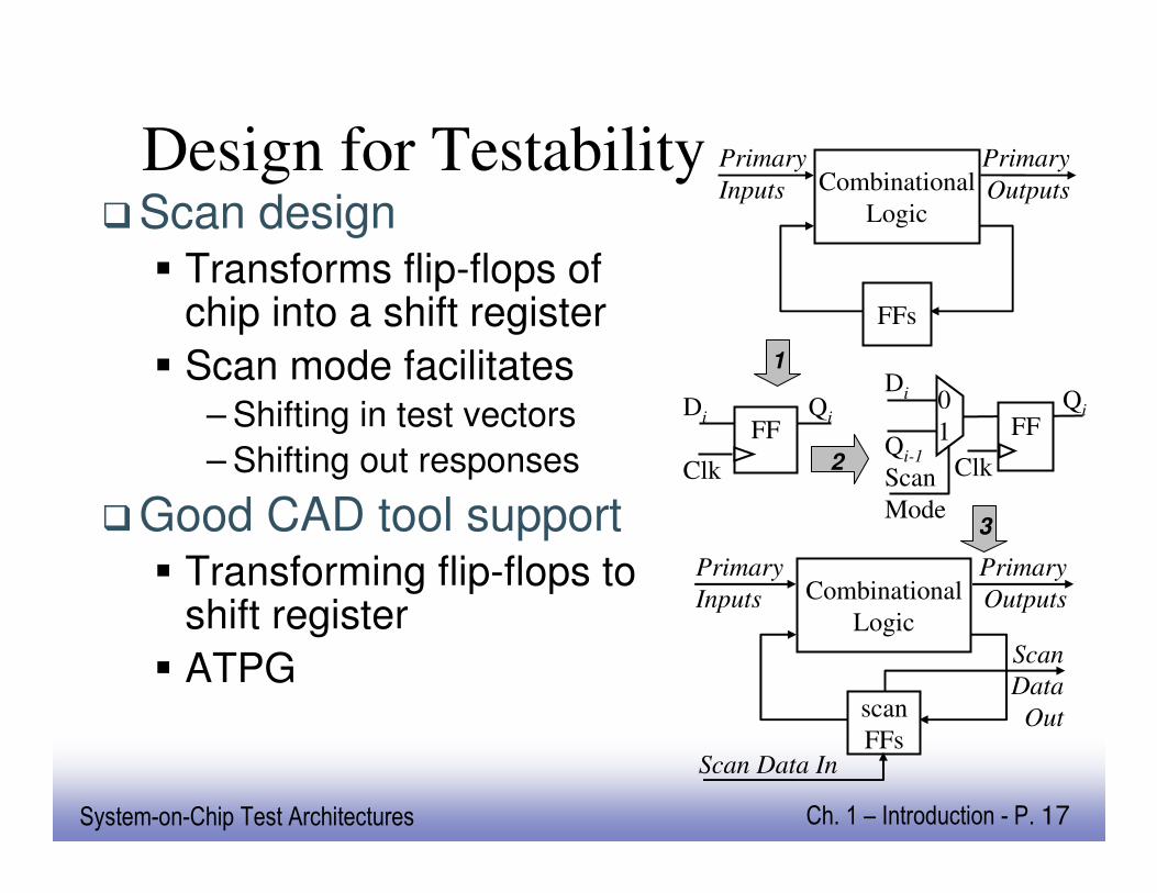
Design for Testability�Scan design
� Transforms flip-flops of chip into a shift register
� Scan mode facilitates– Shifting in test vectors
– Shifting out responses
�Good CAD tool support� Transforming flip-flops to
shift register
� ATPG
FFs
Combinational
Logic
Primary
Inputs
Primary
Outputs
FFDi
Clk
Qi
scan
FFs
Combinational
Logic
Primary
Inputs
Primary
Outputs
Scan Data In
Scan
Data
Out
FF
Clk
Qi
Di
Qi-1
Scan
Mode
0
1
1
2
3
EE141System-on-Chip Test Architectures Ch. 1 – Introduction - P. 18
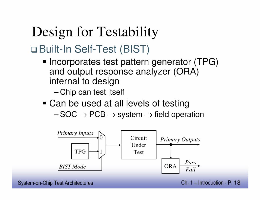
Design for Testability�Built-In Self-Test (BIST)
� Incorporates test pattern generator (TPG) and output response analyzer (ORA) internal to design
– Chip can test itself
� Can be used at all levels of testing– SOC → PCB → system → field operation
TPG
Circuit
Under
Test
Primary InputsPrimary Outputs
BIST Mode ORAPass
Fail
0
1
EE141System-on-Chip Test Architectures Ch. 1 – Introduction - P. 19
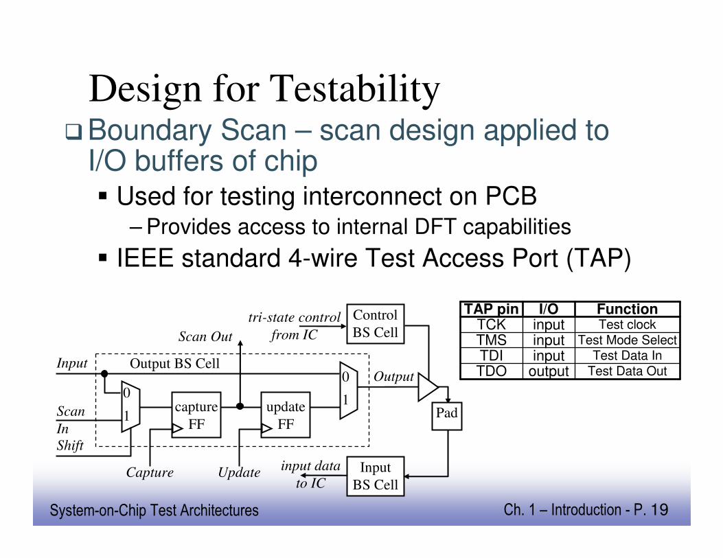
Test Data OutoutputTDOTest Data IninputTDI
Test Mode SelectinputTMSTest clockinputTCKFunctionI/OTAP pin
Design for Testability�Boundary Scan – scan design applied to
I/O buffers of chip� Used for testing interconnect on PCB
– Provides access to internal DFT capabilities
� IEEE standard 4-wire Test Access Port (TAP)
input data
to IC
capture
FF
Capture
update
FF
Update
Input
Scan
In
Shift
Scan Out
Output
Input
BS Cell
Control
BS Cell
Pad
tri-state control
from IC
Output BS Cell
0
1
0
1
EE141System-on-Chip Test Architectures Ch. 1 – Introduction - P. 20
Section 1.2Section 1.2
Basics of SOC TestingBasics of SOC Testing
EE141System-on-Chip Test Architectures Ch. 1 – Introduction - P. 21
IEEE Std. 1149.1 (Boundary
Scan)� Original objective: board-level digital testing
� Now also apply to:
� Chip verification, debugging, clock control, power management, chip reconfiguration, data communication, etc.
� MCM and FPGA
� Analog circuits and high-speed networks
EE141System-on-Chip Test Architectures Ch. 1 – Introduction - P. 22
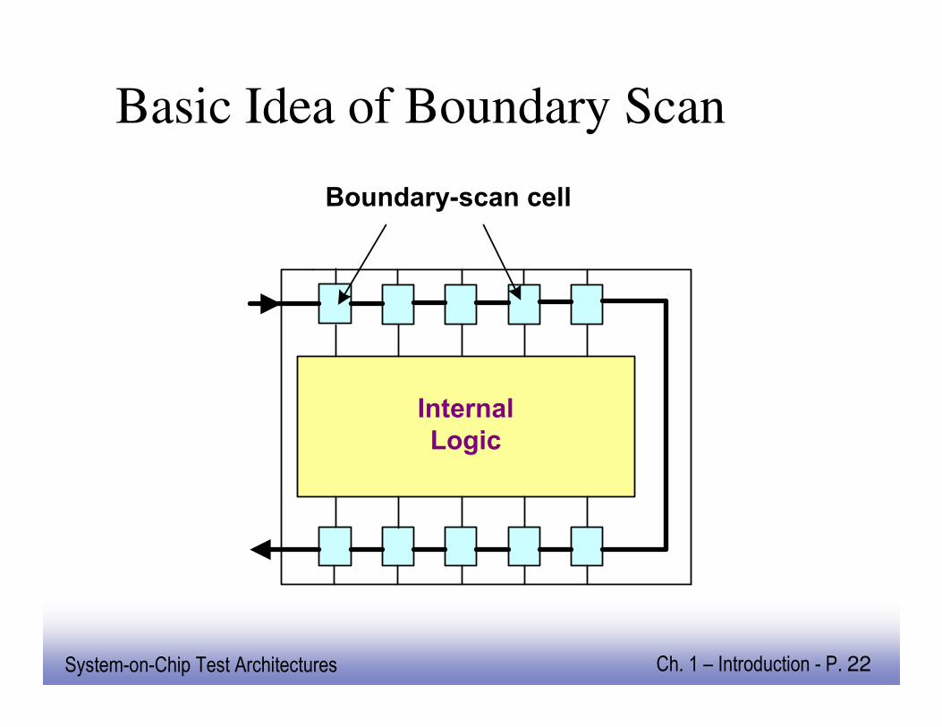
Basic Idea of Boundary Scan
Internal
Logic
Boundary-scan cell
EE141System-on-Chip Test Architectures Ch. 1 – Introduction - P. 23
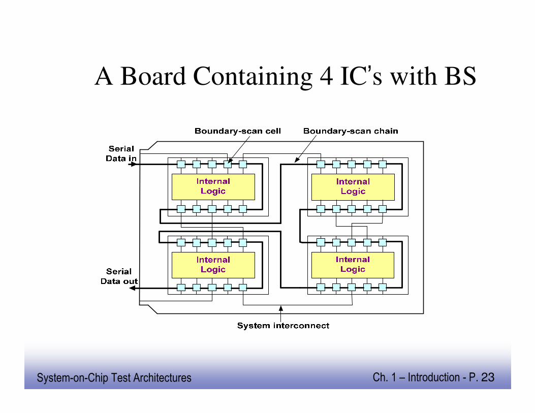
A Board Containing 4 IC’s with BS
EE141System-on-Chip Test Architectures Ch. 1 – Introduction - P. 24
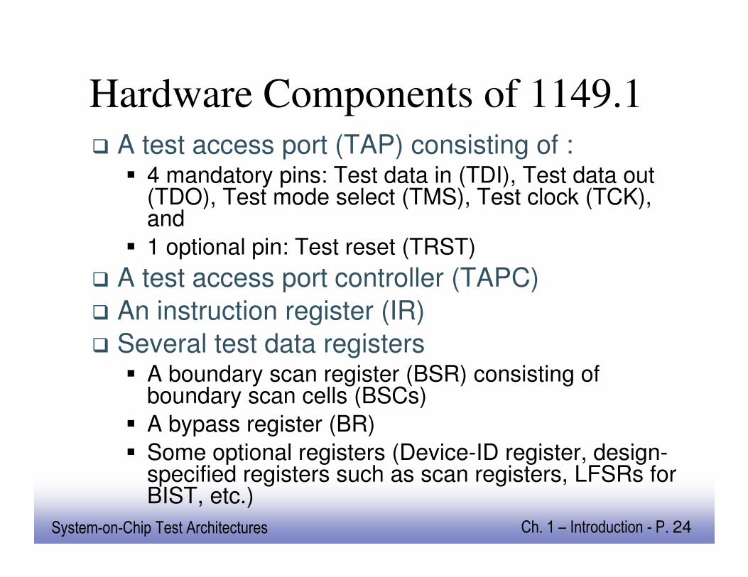
Hardware Components of 1149.1� A test access port (TAP) consisting of :
� 4 mandatory pins: Test data in (TDI), Test data out (TDO), Test mode select (TMS), Test clock (TCK), and
� 1 optional pin: Test reset (TRST)
� A test access port controller (TAPC)
� An instruction register (IR)
� Several test data registers� A boundary scan register (BSR) consisting of
boundary scan cells (BSCs)
� A bypass register (BR)
� Some optional registers (Device-ID register, design-specified registers such as scan registers, LFSRs for BIST, etc.)
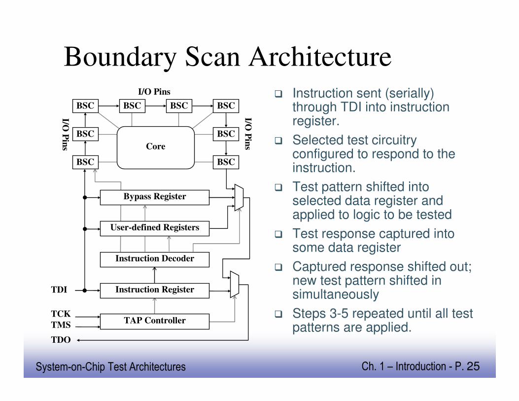
EE141System-on-Chip Test Architectures Ch. 1 – Introduction - P. 25
Boundary Scan Architecture
User-defined Registers
Instruction Decoder
Instruction Register
TAP Controller
Bypass Register
BSC
BSC
BSC
BSC
BSC
BSCBSCBSC
Core
TCK
TMS
TDI
TDO
I/O Pins
I/O P
ins
I/O P
ins
� Instruction sent (serially) through TDI into instruction register.
� Selected test circuitry configured to respond to the instruction.
� Test pattern shifted into selected data register and applied to logic to be tested
� Test response captured into some data register
� Captured response shifted out; new test pattern shifted in simultaneously
� Steps 3-5 repeated until all test patterns are applied.
EE141System-on-Chip Test Architectures Ch. 1 – Introduction - P. 26
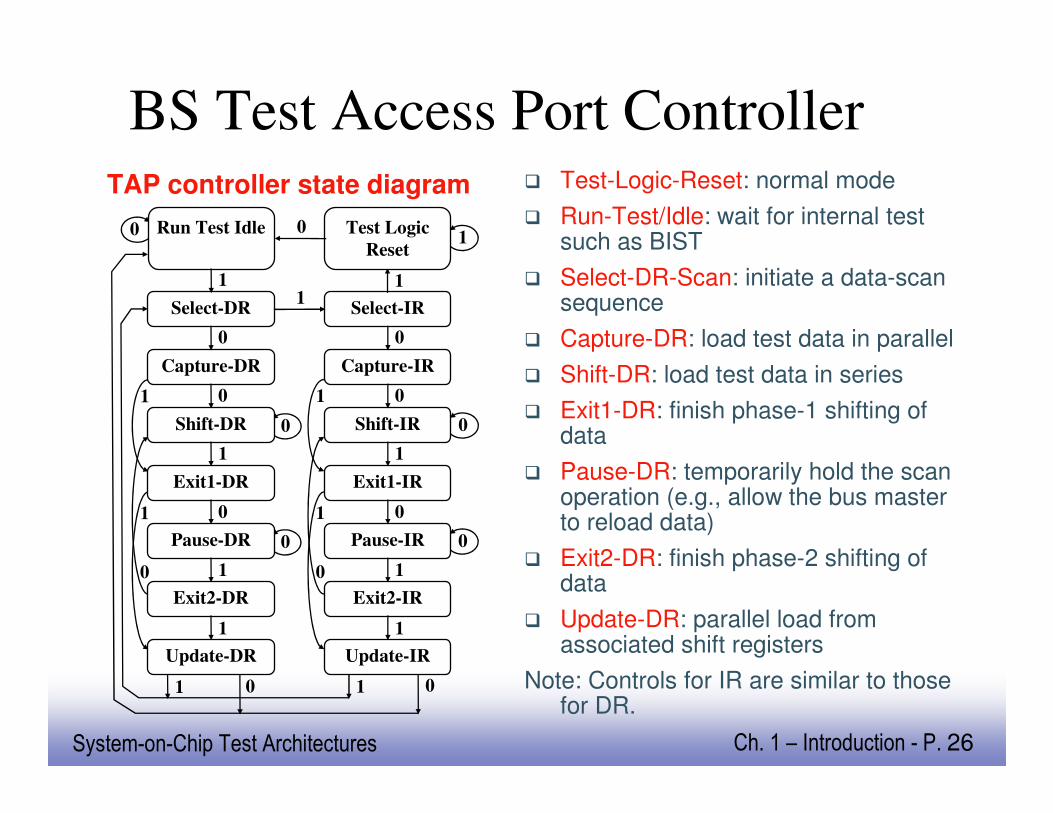
BS Test Access Port Controller
0
1
1
0
1
1
1
0
0
0
0
0
Select-DR
Capture-DR
Shift-DR
Exit1-DR
Pause-DR
Exit2-DR
Update-DR
0
1
0
0
1
1
Select-IR
Capture-IR
Shift-IR
Exit1-IR
Pause-IR
Exit2-IR
Update-IR
0
1
0
0
1
1
Run Test Idle
0
1
1
11
Test Logic
Reset
0
01
TAP controller state diagram � Test-Logic-Reset: normal mode
� Run-Test/Idle: wait for internal test such as BIST
� Select-DR-Scan: initiate a data-scan sequence
� Capture-DR: load test data in parallel
� Shift-DR: load test data in series
� Exit1-DR: finish phase-1 shifting of data
� Pause-DR: temporarily hold the scan operation (e.g., allow the bus master to reload data)
� Exit2-DR: finish phase-2 shifting of data
� Update-DR: parallel load from associated shift registers
Note: Controls for IR are similar to those for DR.
EE141System-on-Chip Test Architectures Ch. 1 – Introduction - P. 27
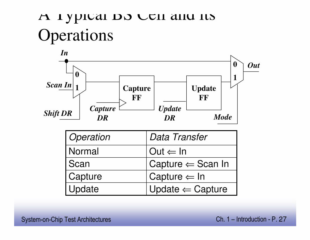
A Typical BS Cell and its
Operations
Capture
FF
Update
FF
Update
DR
Capture
DR
In
Scan In
Shift DR
Out
Mode
0
1
0
1
Update ⇐ CaptureUpdate
Capture ⇐ InCapture
Capture ⇐ Scan InScan
Out ⇐ InNormal
Data TransferOperation
EE141System-on-Chip Test Architectures Ch. 1 – Introduction - P. 28
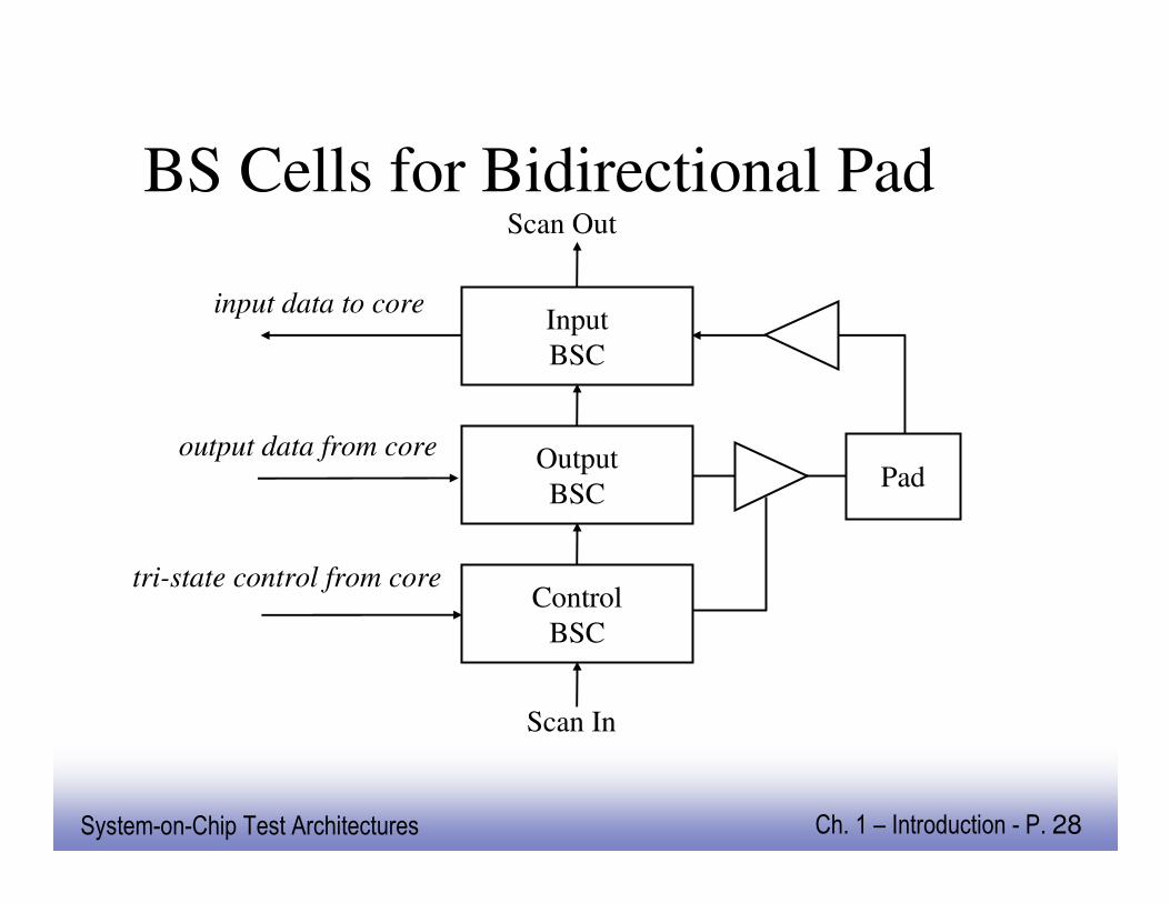
BS Cells for Bidirectional PadScan Out
Input
BSC
Output
BSC
Control
BSC
Scan In
Pad
input data to core
output data from core
tri-state control from core
EE141System-on-Chip Test Architectures Ch. 1 – Introduction - P. 29
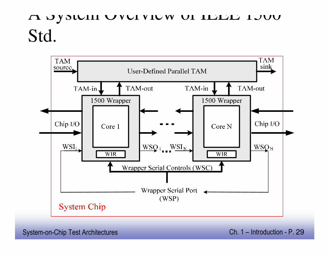
A System Overview of IEEE 1500
Std.
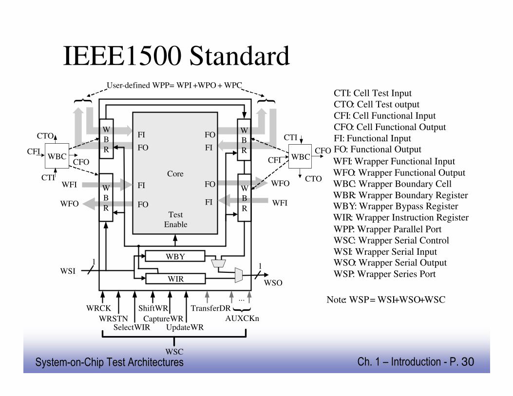
EE141System-on-Chip Test Architectures Ch. 1 – Introduction - P. 30
IEEE1500 Standard
CFO
Note: WSP = WSI+WSO+WSC
CTI: Cell Test Input
CTO: Cell Test output
CFI: Cell Functional Input
CFO: Cell Functional Output
FI: Functional InputFO: Functional Output
WPP: Wrapper Parallel Port
WSC: Wrapper Serial Control
WSI: Wrapper Serial InputWSO: Wrapper Serial Output
WSP: Wrapper Series Port
WFI: Wrapper Functional Input
WFO: Wrapper Functional Output
WBC: Wrapper Boundary Cell
WBR: Wrapper Boundary RegisterWBY: Wrapper Bypass Register
WIR: Wrapper Instruction Register
Core
W
B
R
WBY
W
B
R
WIR
FI
FO
FO
FI
WRCK
WSI
WSO
11
Test
Enable
WFO
WFI
WFI
WFO
WBCCFO
CTO
CTI
CFIWBC
CTI
CTO
CFI
W
B
R
W
B
R
FI
FIFO
FO
User-defined WPP = WPI +WPO + WPC
WRSTNSelectWIR
CaptureWR
ShiftWR
UpdateWR
TransferDR
...
{
AUXCKn
WSC
{ {
EE141System-on-Chip Test Architectures Ch. 1 – Introduction - P. 31
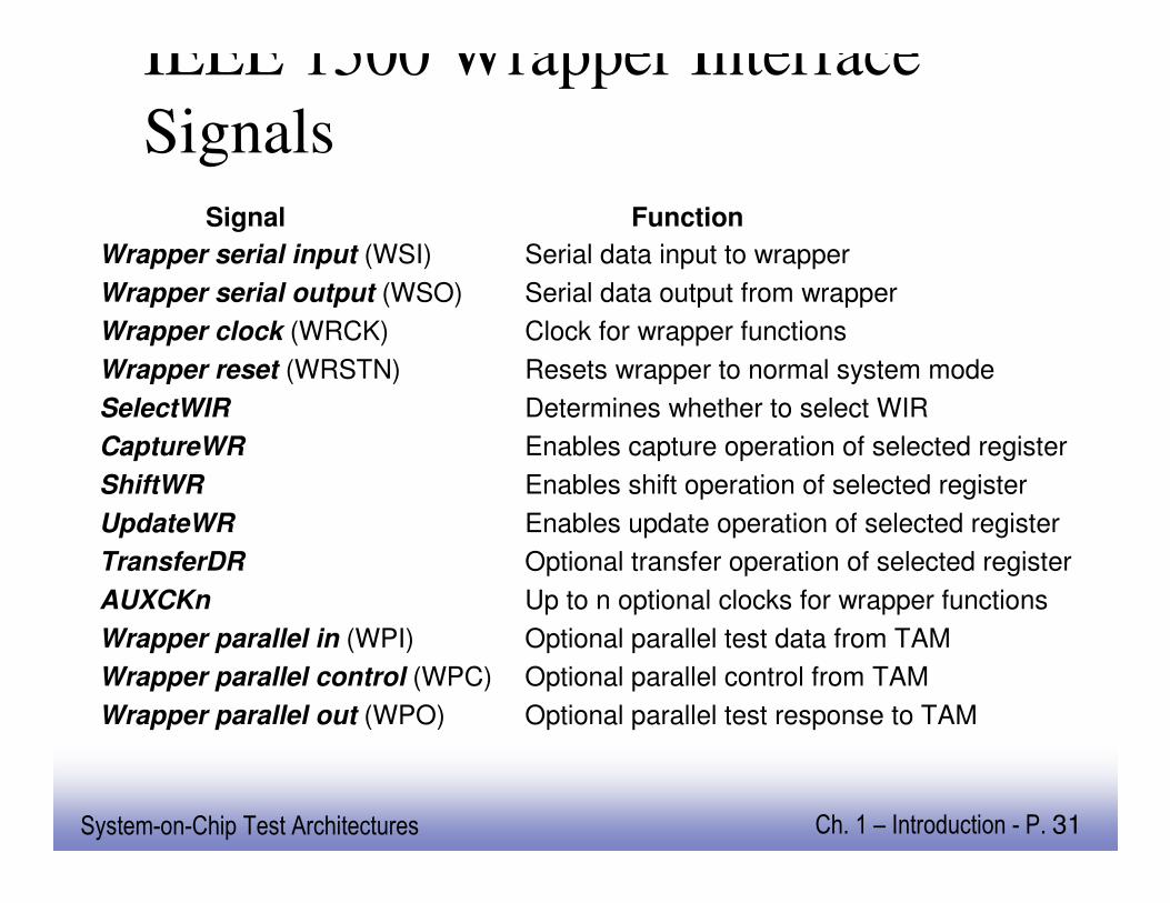
IEEE 1500 Wrapper Interface
SignalsSignal Function
Wrapper serial input (WSI) Serial data input to wrapper
Wrapper serial output (WSO) Serial data output from wrapper
Wrapper clock (WRCK) Clock for wrapper functions
Wrapper reset (WRSTN) Resets wrapper to normal system mode
SelectWIR Determines whether to select WIR
CaptureWR Enables capture operation of selected register
ShiftWR Enables shift operation of selected register
UpdateWR Enables update operation of selected register
TransferDR Optional transfer operation of selected register
AUXCKn Up to n optional clocks for wrapper functions
Wrapper parallel in (WPI) Optional parallel test data from TAM
Wrapper parallel control (WPC) Optional parallel control from TAM
Wrapper parallel out (WPO) Optional parallel test response to TAM
EE141System-on-Chip Test Architectures Ch. 1 – Introduction - P. 32
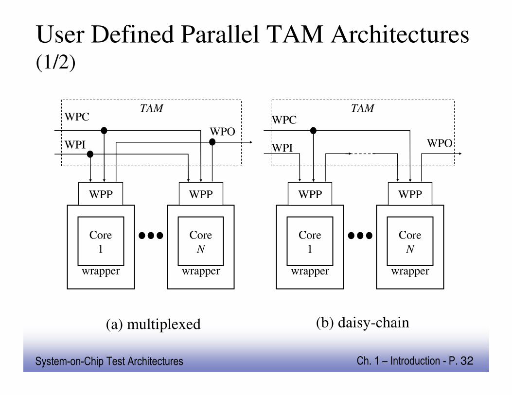
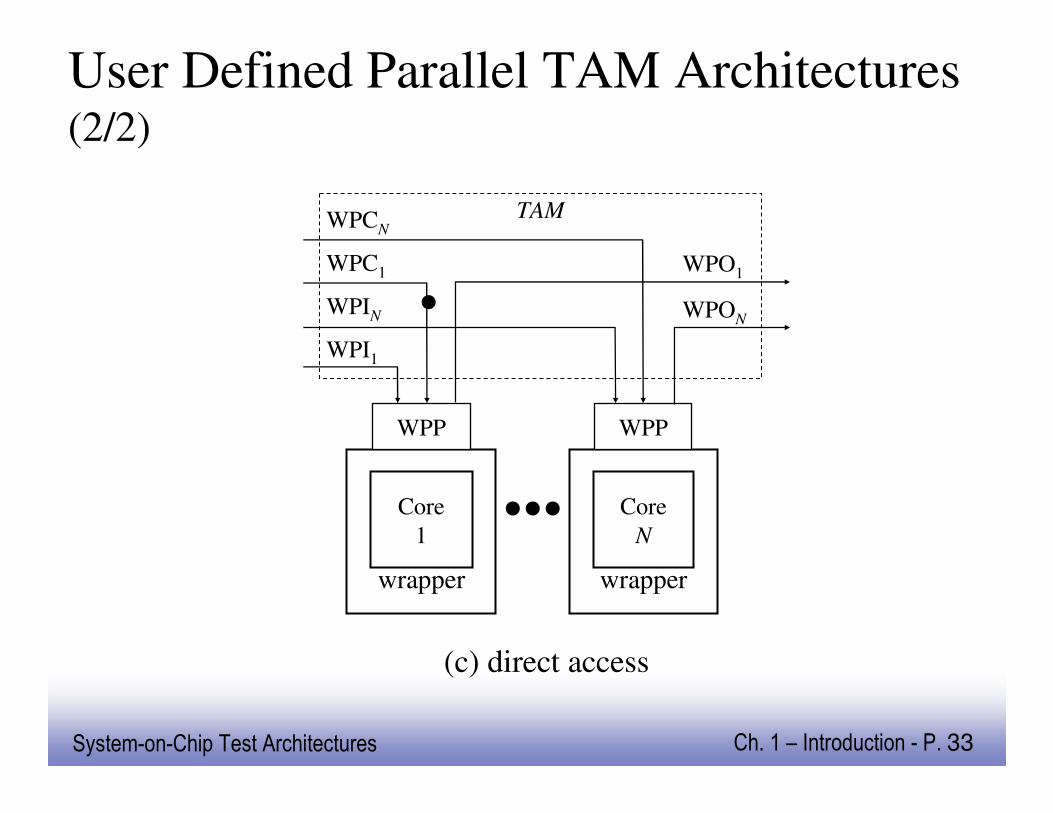
User Defined Parallel TAM Architectures (1/2)
(a) multiplexed
TAM
Core
1
WPP
wrapper
WPC
WPI
Core
N
WPP
wrapper
WPO
(b) daisy-chain
TAM
Core
1
WPP
wrapper
WPC
WPI
Core
N
WPP
wrapper
WPO
EE141System-on-Chip Test Architectures Ch. 1 – Introduction - P. 33
(c) direct access
TAM
Core
1
WPP
wrapper
WPCN
WPC1
WPIN
WPI1
Core
N
WPP
wrapper
WPO1
WPON
User Defined Parallel TAM Architectures (2/2)
EE141System-on-Chip Test Architectures Ch. 1 – Introduction - P. 34
IEEE 1149.6
EE141System-on-Chip Test Architectures Ch. 1 – Introduction - P. 35
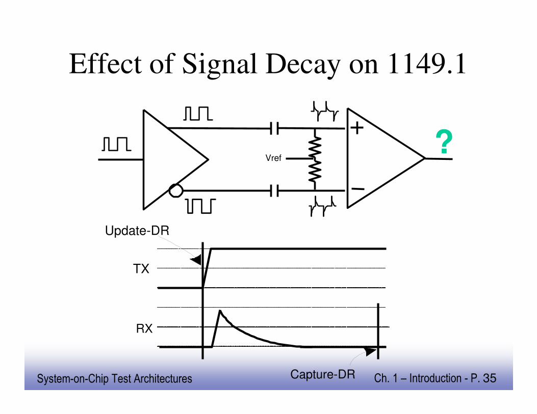
Effect of Signal Decay on 1149.1
?
TX
Update-DR
RX
Capture-DR
Vref
EE141System-on-Chip Test Architectures Ch. 1 – Introduction - P. 36
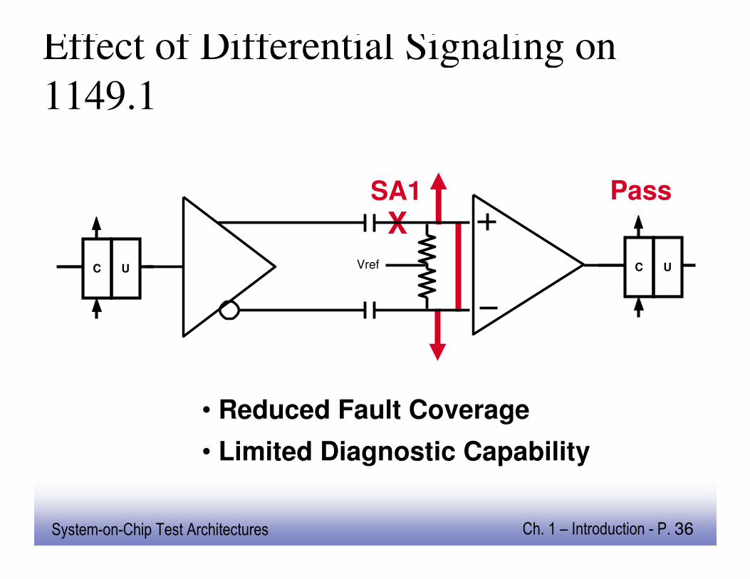
Effect of Differential Signaling on
1149.1
• Reduced Fault Coverage
• Limited Diagnostic Capability
SA1
XPass
VrefC U C U
EE141System-on-Chip Test Architectures Ch. 1 – Introduction - P. 37
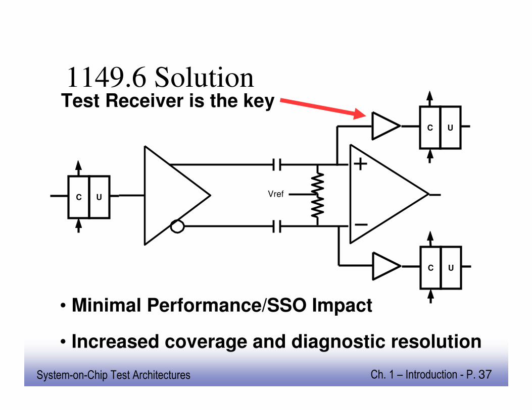
1149.6 Solution
• Minimal Performance/SSO Impact
• Increased coverage and diagnostic resolution
Test Receiver is the key
VrefC U
C U
C U
EE141System-on-Chip Test Architectures Ch. 1 – Introduction - P. 38
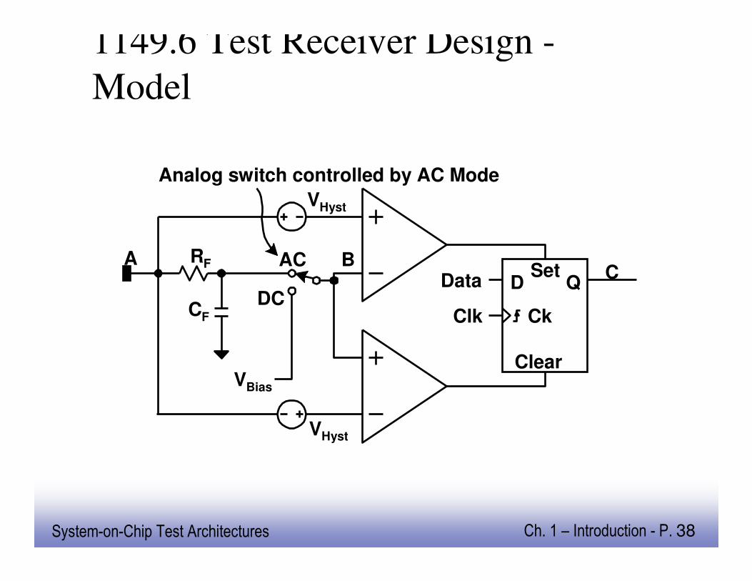
1149.6 Test Receiver Design -
Model
VHyst
Set
Clear
QD
Ck
Data CB
Analog switch controlled by AC Mode
VHyst
Clk
VBias
DC
ACA RF
CF
EE141System-on-Chip Test Architectures Ch. 1 – Introduction - P. 39
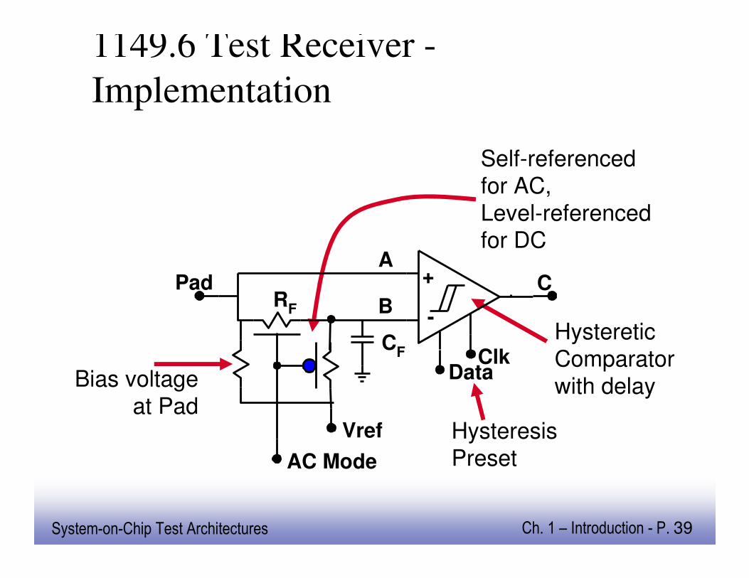
1149.6 Test Receiver -
Implementation
Self-referenced
for AC,
Level-referenced for DC
Bias voltage
at PadHysteresis
Preset
Hysteretic
Comparator
with delay
+
-
AC Mode
Vref
DataClk
A
BC
RF
CF
Pad
EE141System-on-Chip Test Architectures Ch. 1 – Introduction - P. 40
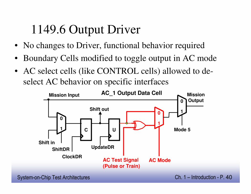
1149.6 Output Driver
• No changes to Driver, functional behavior required
• Boundary Cells modified to toggle output in AC mode
• AC select cells (like CONTROL cells) allowed to de-
select AC behavior on specific interfaces
0
1
0
1 C U
ShiftDR
Shift in
ClockDR
UpdateDR
Mode 5
Shift out0
1
AC ModeAC Test Signal(Pulse or Train)
AC_1 Output Data CellMission Input Mission
Output
EE141System-on-Chip Test Architectures Ch. 1 – Introduction - P. 41
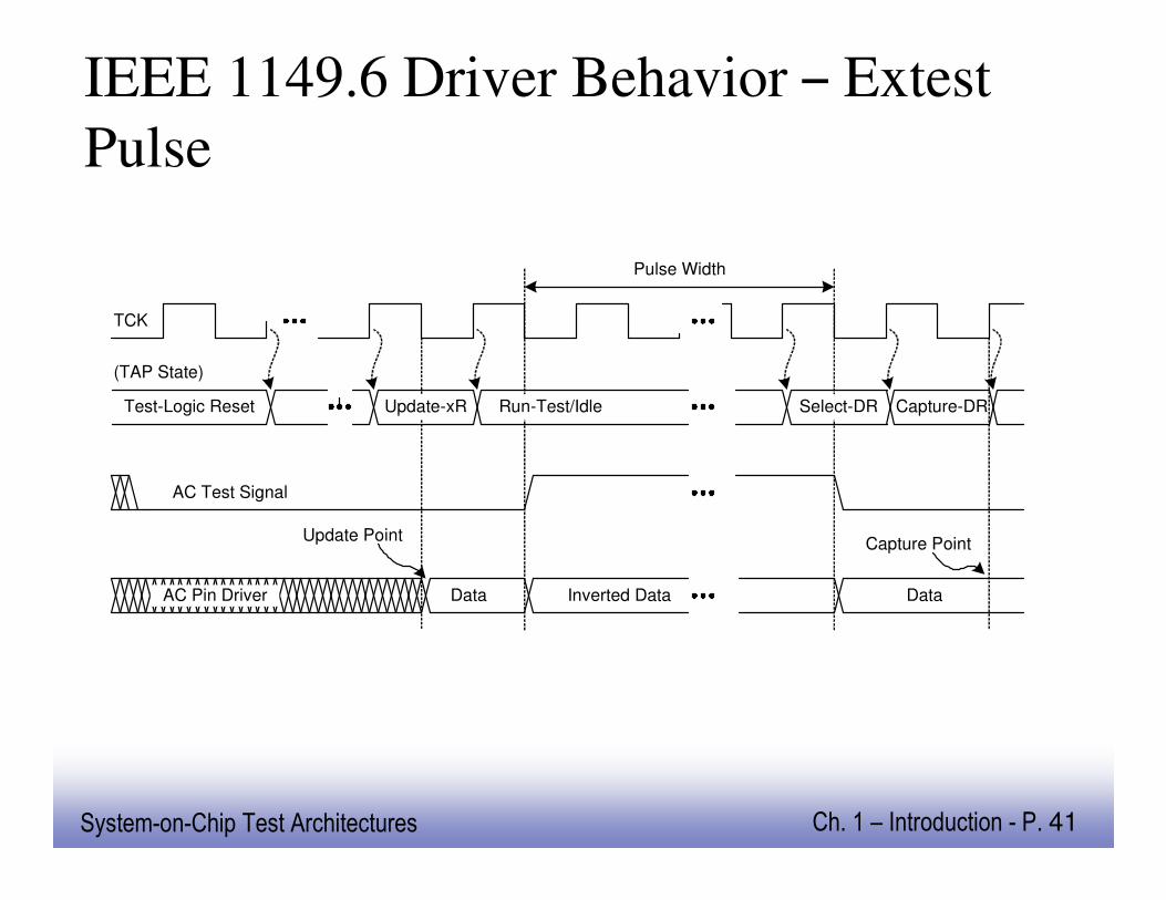
IEEE 1149.6 Driver Behavior – Extest
Pulse
TCK
Capture PointUpdate Point
(TAP State)
Test-Logic Reset Select-DR Capture-DR
AC Test Signal
Data Inverted Data Data
Pulse Width
Update-xR Run-Test/Idle
AC Pin Driver
EE141System-on-Chip Test Architectures Ch. 1 – Introduction - P. 42
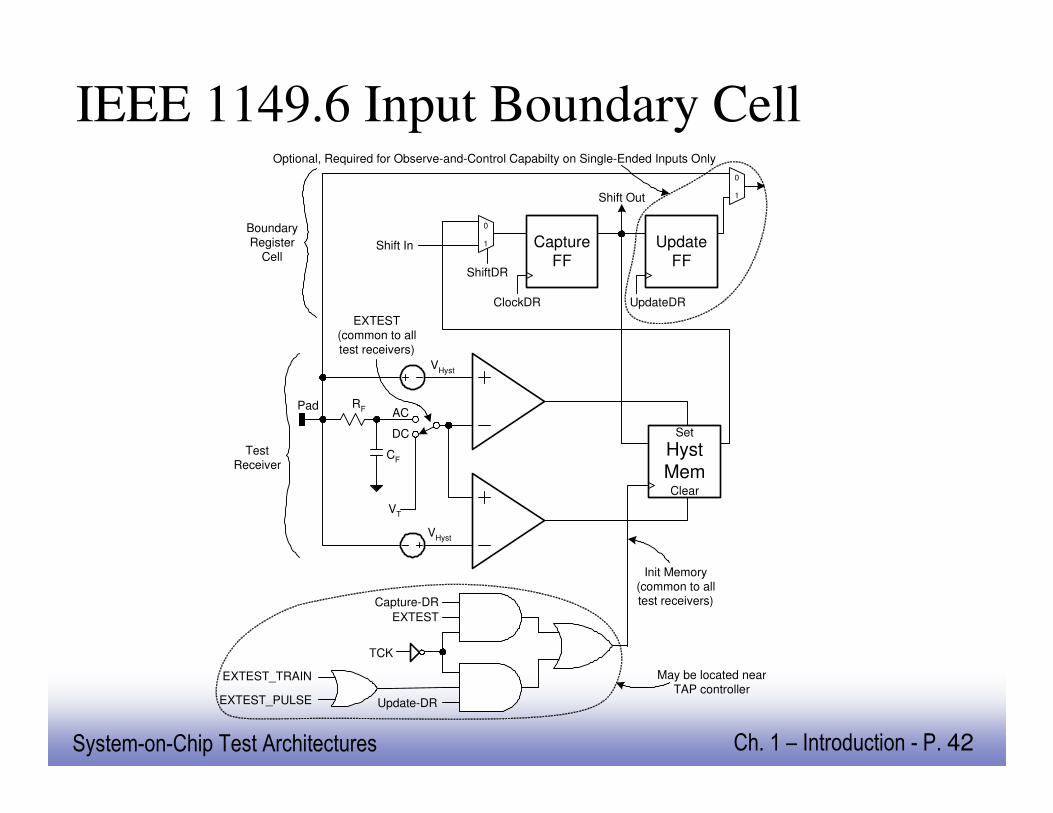
IEEE 1149.6 Input Boundary Cell
VHyst
VHyst
Pad RF
CF
VT
DC
AC
EXTEST(common to alltest receivers)
Hyst
MemClear
Set
Shift In
TCK
Update-DR
Capture-DR
EXTEST
May be located nearTAP controller
Init Memory(common to alltest receivers)
Capture
FF
Update
FF
ClockDR
0
1
ShiftDR
Shift Out
UpdateDR
0
1
Optional, Required for Observe-and-Control Capabilty on Single-Ended Inputs Only
BoundaryRegister
Cell
TestReceiver
EXTEST_TRAIN
EXTEST_PULSE
EE141System-on-Chip Test Architectures Ch. 1 – Introduction - P. 43
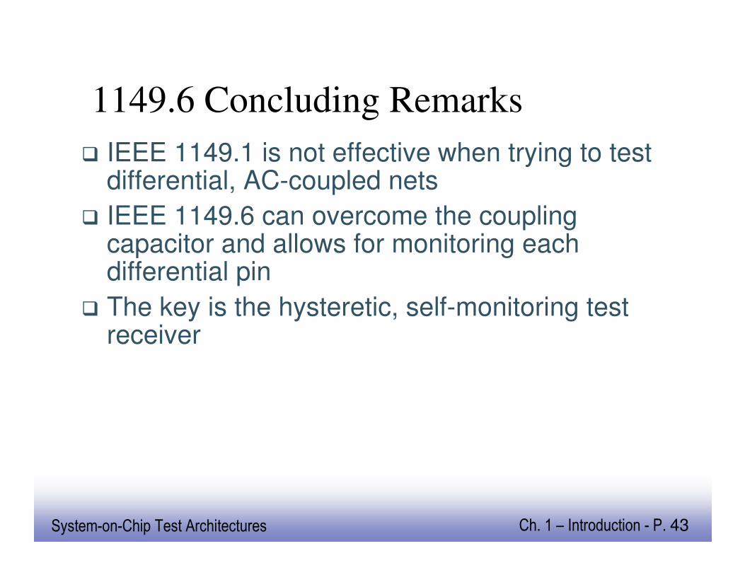
1149.6 Concluding Remarks
� IEEE 1149.1 is not effective when trying to test differential, AC-coupled nets
� IEEE 1149.6 can overcome the coupling capacitor and allows for monitoring each differential pin
� The key is the hysteretic, self-monitoring test receiver
EE141System-on-Chip Test Architectures Ch. 1 – Introduction - P. 44
IEEE P1687
(IJTAG)
EE141System-on-Chip Test Architectures Ch. 1 – Introduction - P. 45
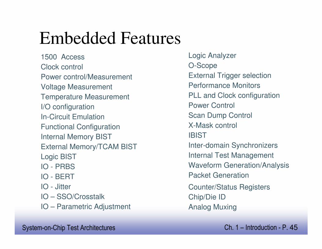
Embedded Features
IO – Parametric Adjustment
IO – SSO/Crosstalk
IO - Jitter
IO - BERT
IO - PRBS
Logic BIST
External Memory/TCAM BIST
Internal Memory BIST
Functional Configuration
In-Circuit Emulation
I/O configuration
Temperature Measurement
Voltage Measurement
Power control/Measurement
Clock control
1500 Access
Analog Muxing
Chip/Die ID
Counter/Status Registers
Packet Generation
Waveform Generation/Analysis
Internal Test Management
Inter-domain Synchronizers
IBIST
X-Mask control
Scan Dump Control
Power Control
PLL and Clock configuration
Performance Monitors
External Trigger selection
O-Scope
Logic Analyzer
EE141System-on-Chip Test Architectures Ch. 1 – Introduction - P. 46
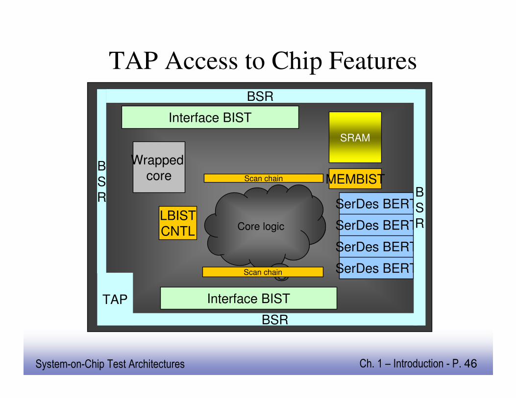
TAP Access to Chip Features
SRAM
MEMBIST
Interface BIST
Interface BIST
Core logicLBISTCNTL
Scan chain
Scan chain
SerDes BERT
SerDes BERT
SerDes BERT
SerDes BERT
TAP
BSR B
SR
BSR
BSR
Wrapped core
EE141System-on-Chip Test Architectures Ch. 1 – Introduction - P. 47
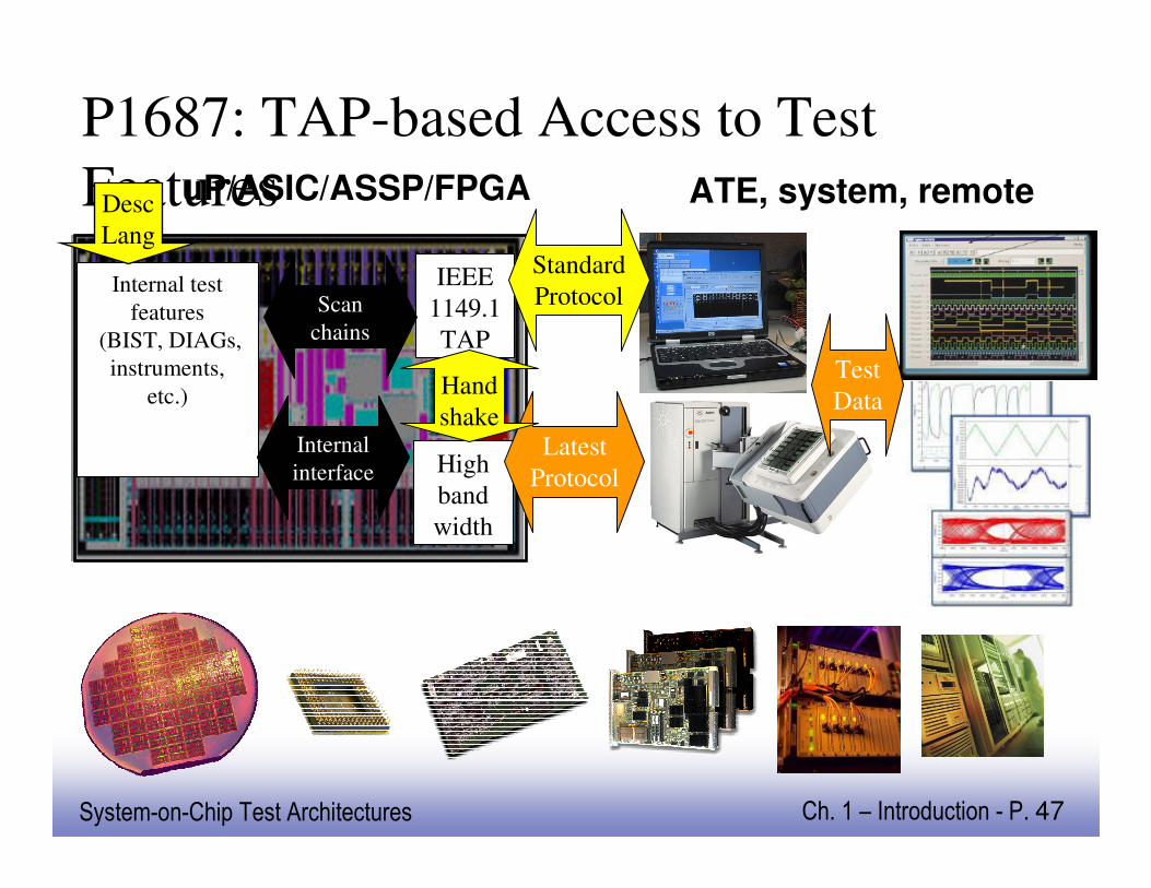
uP/ASIC/ASSP/FPGA
IEEE
1149.1
TAP
Scan
chains
Internal test
features
(BIST, DIAGs,
instruments,
etc.)
P1687: TAP-based Access to Test
Features
Standard
Protocol
ATE, system, remote
High
band
width
Internal
interfaceLatest
Protocol
Hand
shake
Test
Data
Desc
Lang
EE141System-on-Chip Test Architectures Ch. 1 – Introduction - P. 48
Basic P1687 Questions and Answers
� What is P1687?
� How does it work?
� Why do we need it?
IEEE P1687 -- Draft Standard for Access and Control of Instrumentation Embedded Within a Semiconductor Device
P1687 will provide standardized procedural access to make on-chip test & debug features available
To enable use and re-use of DFT features at all stages of product life cycle
EE141System-on-Chip Test Architectures Ch. 1 – Introduction - P. 49
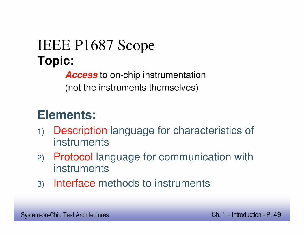
IEEE P1687 ScopeTopic:
Access to on-chip instrumentation
(not the instruments themselves)
Elements:
1) Description language for characteristics of instruments
2) Protocol language for communication with instruments
3) Interface methods to instruments
EE141System-on-Chip Test Architectures Ch. 1 – Introduction - P. 50
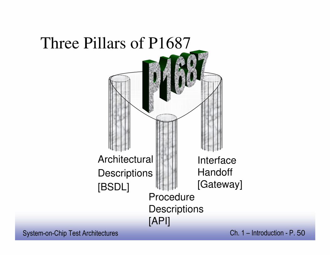
Three Pillars of P1687
Architectural
Descriptions
[BSDL]
InterfaceHandoff
[Gateway]
Procedure
Descriptions [API]
EE141System-on-Chip Test Architectures Ch. 1 – Introduction - P. 51
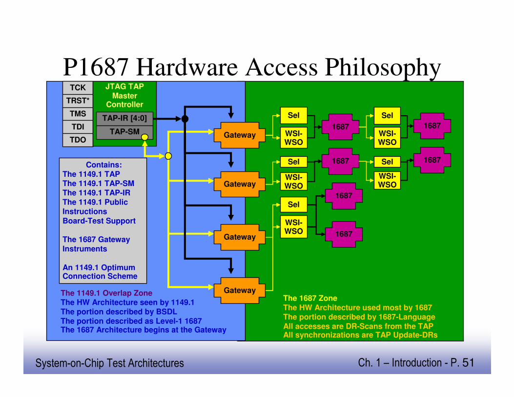
P1687 Hardware Access Philosophy
Sel
WSI-WSO
1687
1687Sel
WSI-WSO
Sel
WSI-WSO
Sel
WSI-WSO
1687Sel
WSI-WSO
The 1687 ZoneThe HW Architecture used most by 1687The portion described by 1687-LanguageAll accesses are DR-Scans from the TAPAll synchronizations are TAP Update-DRs
1687
1687
1687
TCK
TRST*
TMS
TDI
TDO
JTAG TAPMaster
Controller
TAP-IR [4:0]
Contains:The 1149.1 TAPThe 1149.1 TAP-SMThe 1149.1 TAP-IRThe 1149.1 PublicInstructionsBoard-Test Support
The 1687 GatewayInstruments
An 1149.1 Optimum Connection Scheme
TAP-SM
The 1149.1 Overlap ZoneThe HW Architecture seen by 1149.1The portion described by BSDLThe portion described as Level-1 1687The 1687 Architecture begins at the Gateway
Gateway
Gateway
Gateway
Gateway
EE141System-on-Chip Test Architectures Ch. 1 – Introduction - P. 52
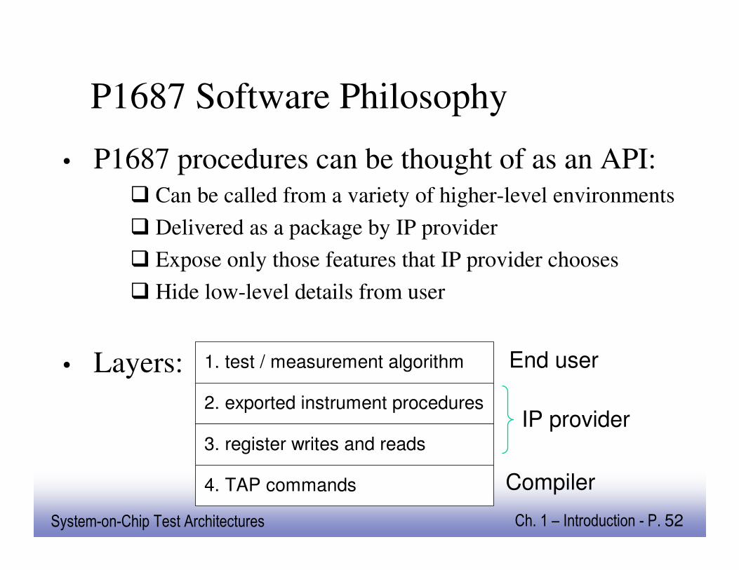
P1687 Software Philosophy
• P1687 procedures can be thought of as an API:
� Can be called from a variety of higher-level environments
� Delivered as a package by IP provider
� Expose only those features that IP provider chooses
� Hide low-level details from user
• Layers: 1. test / measurement algorithm
2. exported instrument procedures
3. register writes and reads
4. TAP commands
End user
IP provider
Compiler
EE141System-on-Chip Test Architectures Ch. 1 – Introduction - P. 53
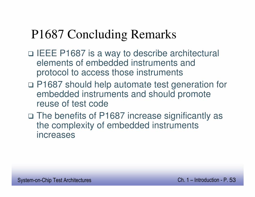
P1687 Concluding Remarks
� IEEE P1687 is a way to describe architectural elements of embedded instruments and protocol to access those instruments
� P1687 should help automate test generation for embedded instruments and should promote reuse of test code
� The benefits of P1687 increase significantly as the complexity of embedded instruments increases
EE141System-on-Chip Test Architectures Ch. 1 – Introduction - P. 54
IEEE Std. 1149.4
Standard for a MixedStandard for a Mixed--Signal BusSignal Bus
EE141System-on-Chip Test Architectures Ch. 1 – Introduction - P. 55
11.4 IEEE Std. 1149.4 Standard for
a Mixed-Signal Test Bus
� IEEE Std. 1149.4 Overview
� IEEE Std. 1149.4 Circuit Structures
� IEEE Std. 1149.4 Instructions
� IEEE Std. 1149.4 Test Modes
EE141System-on-Chip Test Architectures Ch. 1 – Introduction - P. 56
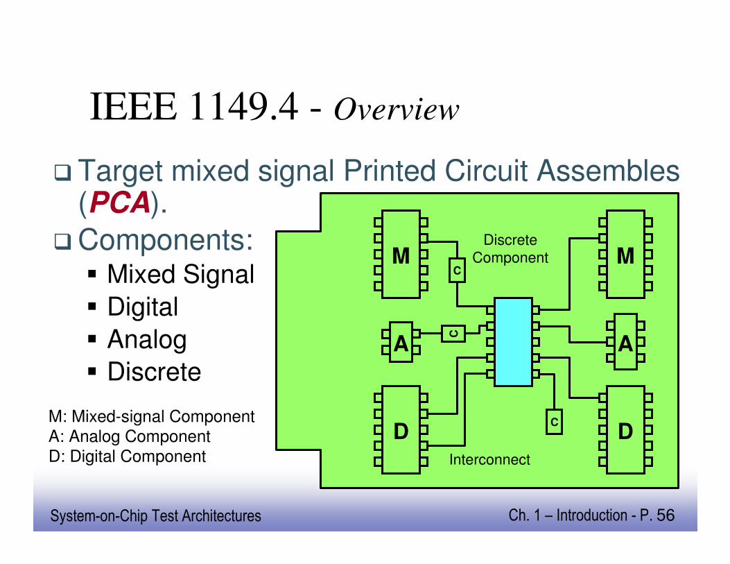
IEEE 1149.4 - Overview
� Target mixed signal Printed Circuit Assembles (PCA).
� Components:� Mixed Signal
� Digital
� Analog
� Discrete
D D
A A
M MC
C
CInterconnect
Discrete
Component
M: Mixed-signal Component
A: Analog Component
D: Digital Component
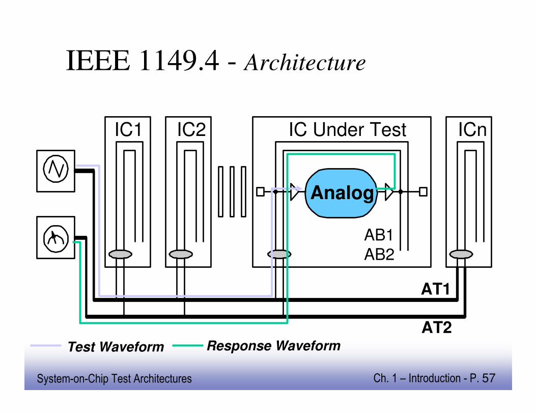
EE141System-on-Chip Test Architectures Ch. 1 – Introduction - P. 57
IEEE 1149.4 - Architecture
IC1 IC2 ICnIC Under Test
Analog
AT1
AT2
AB1
AB2
Test Waveform Response Waveform
EE141System-on-Chip Test Architectures Ch. 1 – Introduction - P. 58
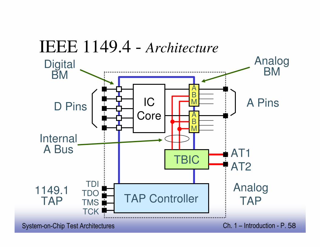
IEEE 1149.4 - Architecture
IC
Core
DigitalBM
ABM
ABM
AnalogBM
A Pins
TBIC
Analog
TAP
AT1
AT2
TAP Controller1149.1
TAP
TDITDOTMSTCK
D Pins
InternalA Bus
EE141System-on-Chip Test Architectures Ch. 1 – Introduction - P. 59
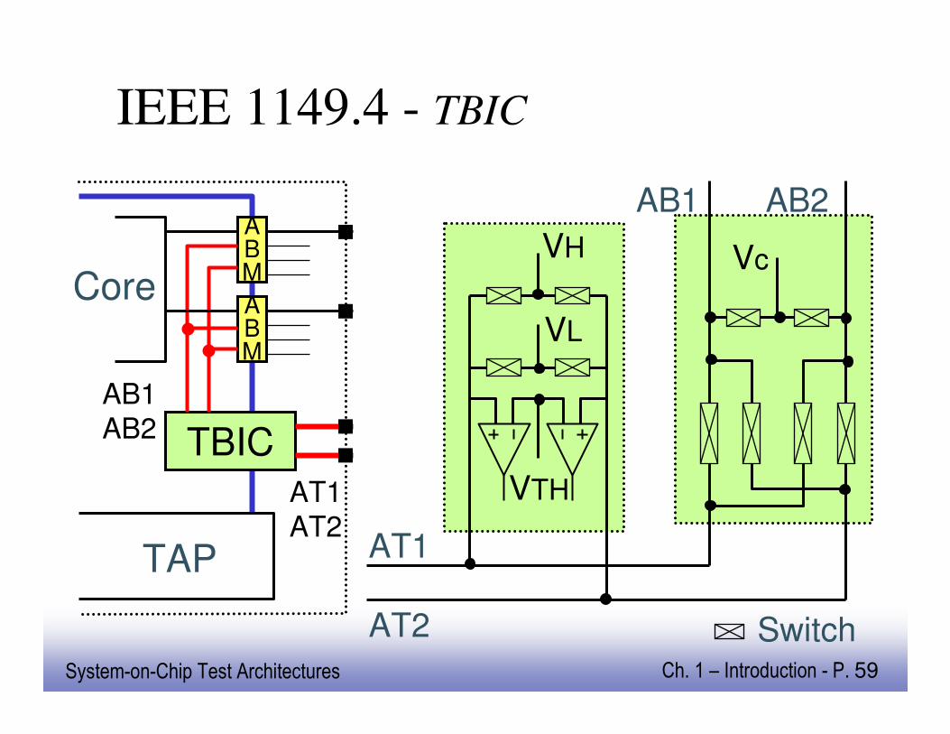
IEEE 1149.4 - TBIC
VH
VL
VTH
ABM
ABM
TBIC
Core
TAP
AB1
AB2
AT2
Vc
AB1 AB2
Switch
AT1
AT1
AT2
EE141System-on-Chip Test Architectures Ch. 1 – Introduction - P. 60
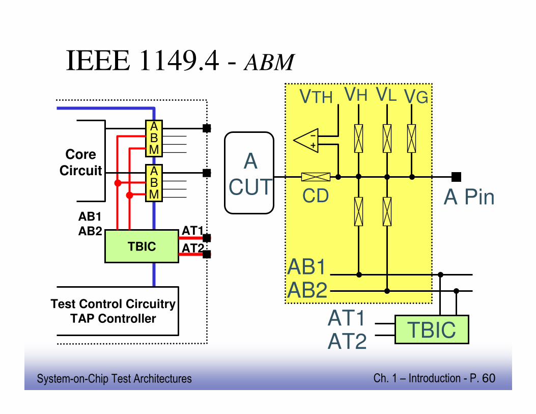
IEEE 1149.4 - ABM
AT1AT2
AB1AB2
VH VLVTH VG
A PinCD
ACUT
TBIC
ABM
ABM
TBIC
CoreCircuit
Test Control CircuitryTAP Controller
AB1AB2 AT1
AT2
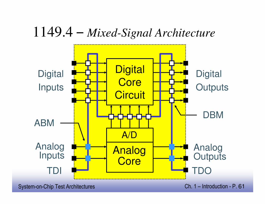
EE141System-on-Chip Test Architectures Ch. 1 – Introduction - P. 61
1149.4 – Mixed-Signal Architecture
DigitalCore
Circuit
AnalogInputs
A/D
AnalogCore
TDI TDO
AnalogOutputs
Digital
Inputs
Digital
Outputs
DBMABM
EE141System-on-Chip Test Architectures Ch. 1 – Introduction - P. 62
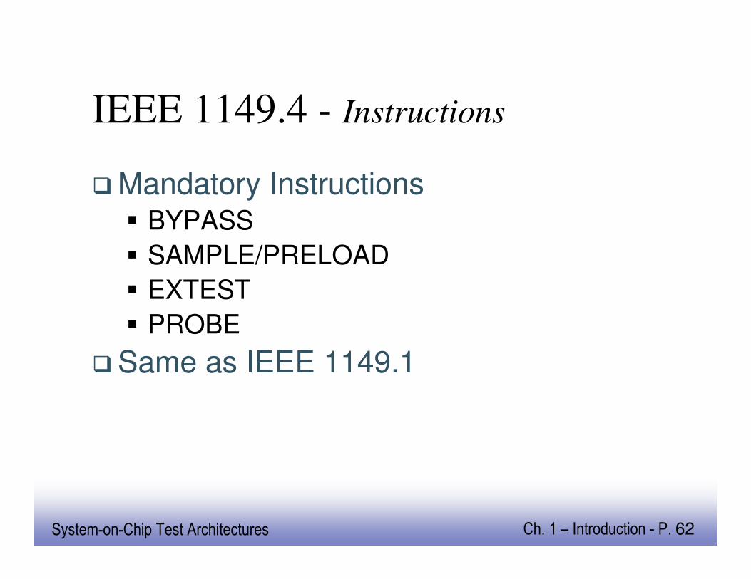
IEEE 1149.4 - Instructions
� Mandatory Instructions� BYPASS
� SAMPLE/PRELOAD
� EXTEST
� PROBE
� Same as IEEE 1149.1
EE141System-on-Chip Test Architectures Ch. 1 – Introduction - P. 63
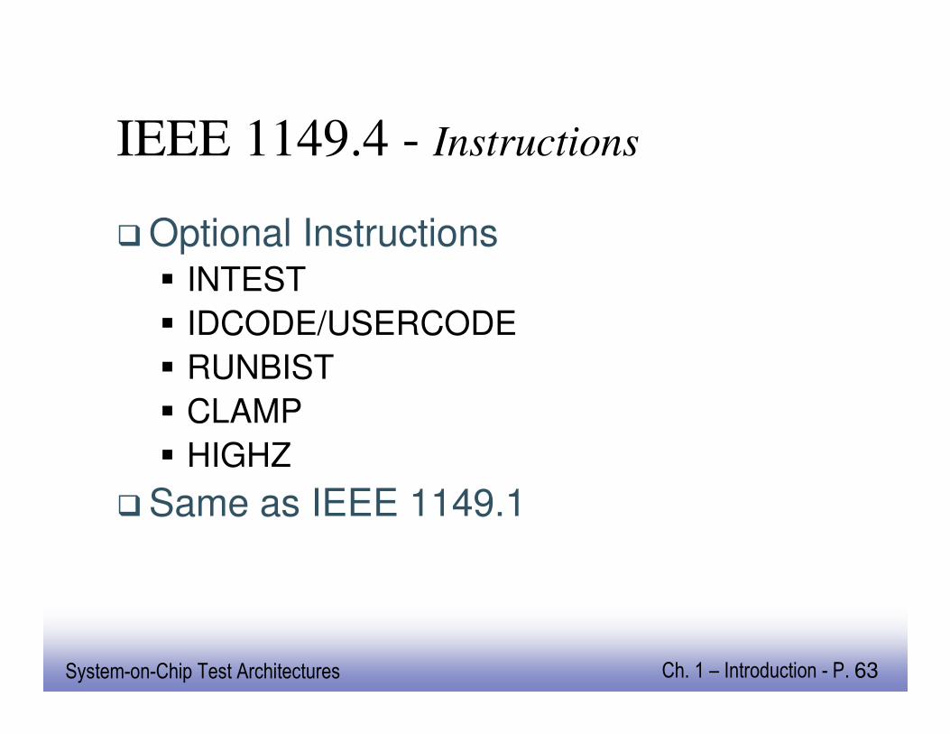
IEEE 1149.4 - Instructions
� Optional Instructions� INTEST
� IDCODE/USERCODE
� RUNBIST
� CLAMP
� HIGHZ
� Same as IEEE 1149.1
EE141System-on-Chip Test Architectures Ch. 1 – Introduction - P. 64
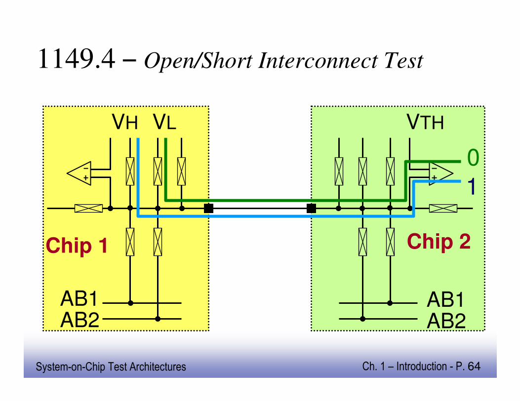
1149.4 – Open/Short Interconnect Test
AB1AB2
VH VL
AB1AB2
VTH
Chip 1 Chip 2
1
0
EE141System-on-Chip Test Architectures Ch. 1 – Introduction - P. 65
Concluding Remarks
� IEEE 1149.4 is an extension of 1149.1 for mixed-signal and analog testing.
� Two major building blocks:� ABM: Analog Boundary Module
� TBIC: Test Bus Interface Circuit
� Four mandatory instructions:� Bypass, Sample/Preload, EXTEST, PROBE
� Supports:� Interconnect Test, Parametric Test, Internal Test
� Major drawback: Parasitic effects associated with the long buses.
EE141System-on-Chip Test Architectures Ch. 1 – Introduction - P. 66
Section 1.3Section 1.3
Basics of Memory TestingBasics of Memory Testing
EE141System-on-Chip Test Architectures Ch. 1 – Introduction - P. 67
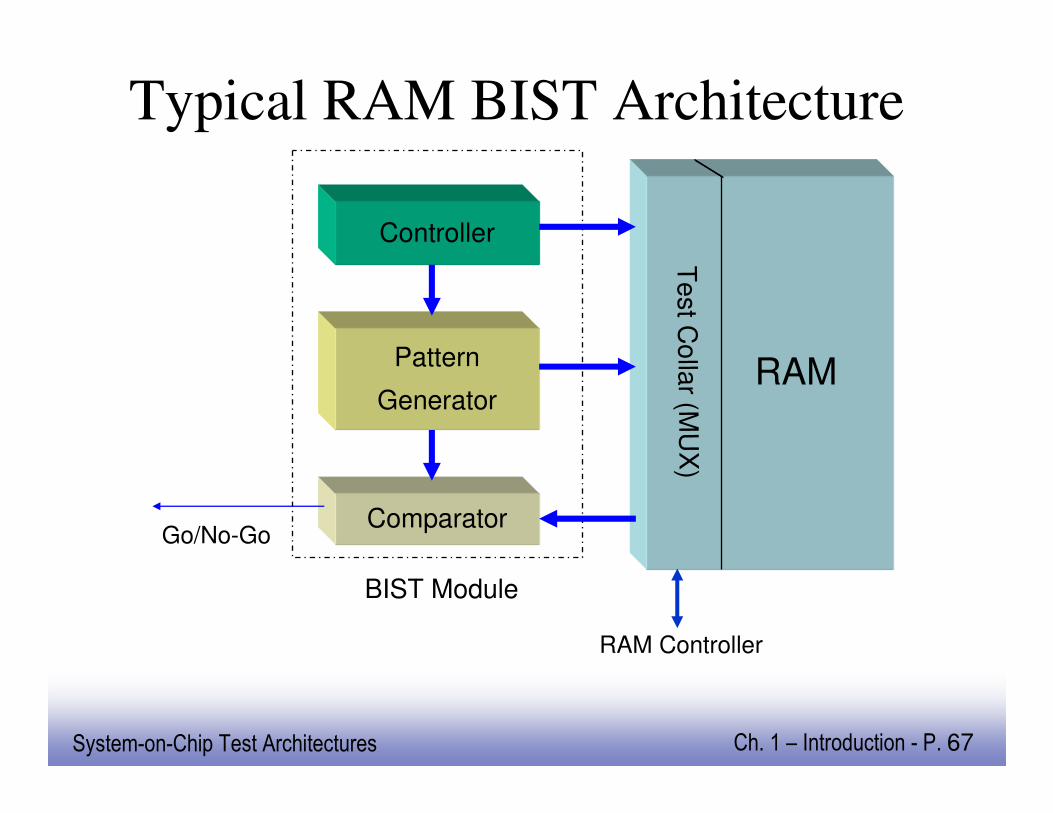
Typical RAM BIST Architecture
RAMT
est C
ol la
r ( MU
X)
BIST Module
Controller
Comparator
Pattern
Generator
Go/No-Go
RAM Controller
EE141System-on-Chip Test Architectures Ch. 1 – Introduction - P. 68
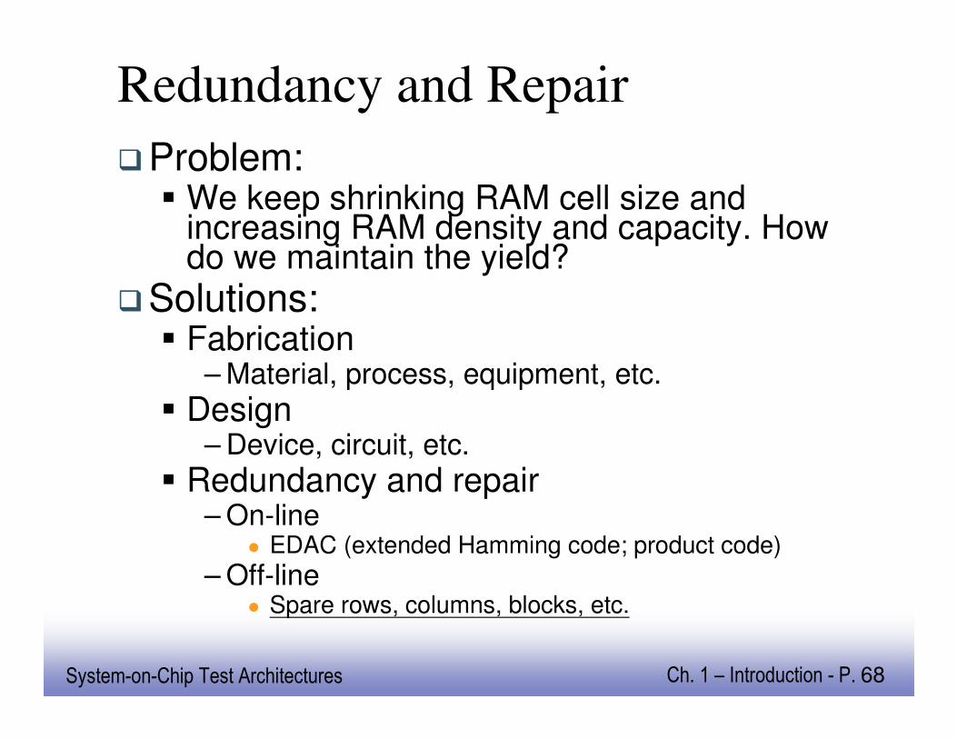
Redundancy and Repair
�Problem:� We keep shrinking RAM cell size and
increasing RAM density and capacity. How do we maintain the yield?
�Solutions:� Fabrication
– Material, process, equipment, etc.
� Design– Device, circuit, etc.
� Redundancy and repair– On-line
� EDAC (extended Hamming code; product code)
– Off-line� Spare rows, columns, blocks, etc.
EE141System-on-Chip Test Architectures Ch. 1 – Introduction - P. 69
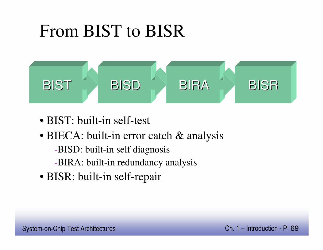
From BIST to BISR
BISTBIST BISDBISD BIRABIRA BISRBISR
•• BIST: built-in self-test
• BIECA: built-in error catch & analysis
-BISD: built-in self diagnosis
-BIRA: built-in redundancy analysis
• BISR: built-in self-repair
EE141System-on-Chip Test Architectures Ch. 1 – Introduction - P. 70
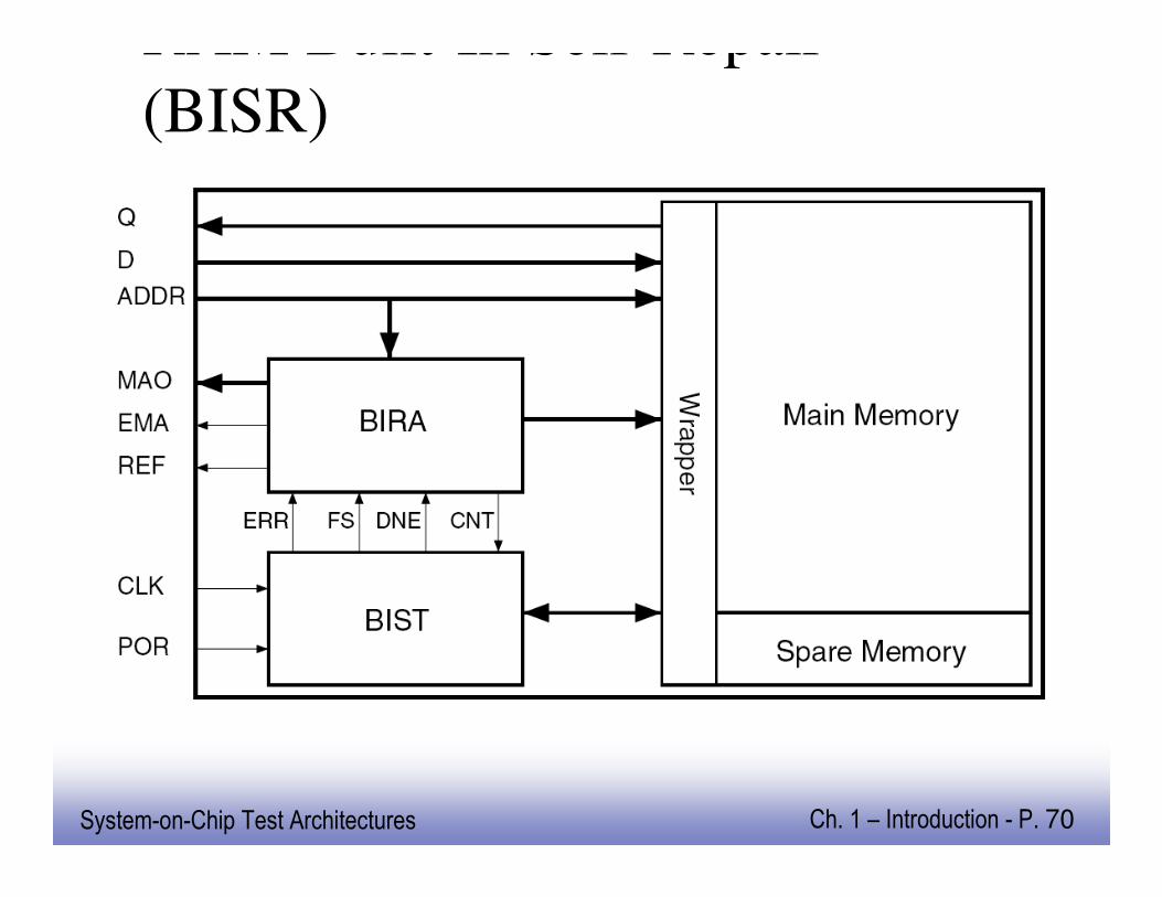
RAM Built-In Self-Repair
(BISR)
EE141System-on-Chip Test Architectures Ch. 1 – Introduction - P. 71
Section 1.4Section 1.4
SOC Design ExamplesSOC Design Examples
EE141System-on-Chip Test Architectures Ch. 1 – Introduction - P. 72
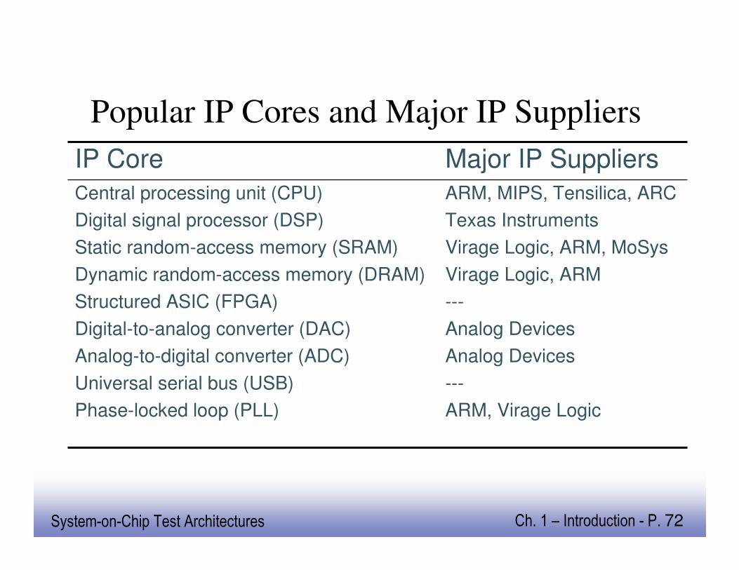
Popular IP Cores and Major IP Suppliers
ARM, MIPS, Tensilica, ARC
Texas Instruments
Virage Logic, ARM, MoSys
Virage Logic, ARM
---
Analog Devices
Analog Devices
---
ARM, Virage Logic
Central processing unit (CPU)
Digital signal processor (DSP)
Static random-access memory (SRAM)
Dynamic random-access memory (DRAM)
Structured ASIC (FPGA)
Digital-to-analog converter (DAC)
Analog-to-digital converter (ADC)
Universal serial bus (USB)
Phase-locked loop (PLL)
Major IP SuppliersIP Core
EE141System-on-Chip Test Architectures Ch. 1 – Introduction - P. 73
Example 1: BioMEMS Sensor
� The wireless bioMEMS sensor developed at National Taiwan University is the first wearable prototype to detect C-reactive protein (CRP) based on nanomechanics[Chen 2006].
EE141System-on-Chip Test Architectures Ch. 1 – Introduction - P. 74
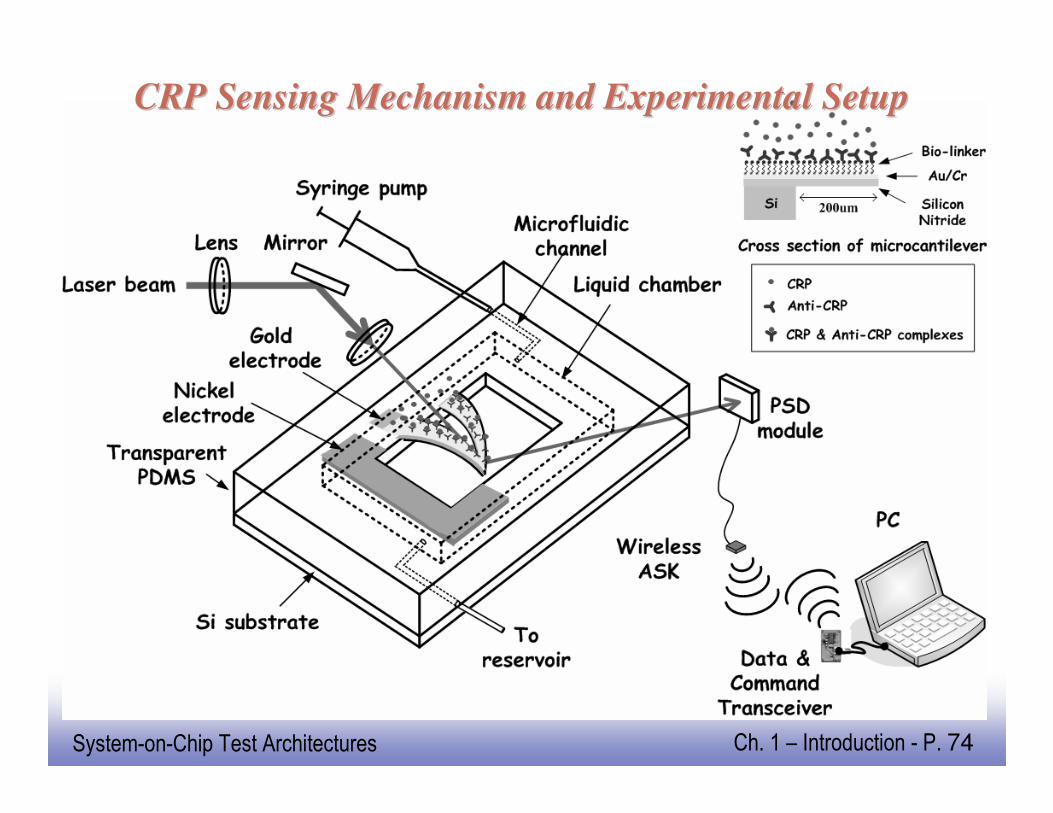
CRP Sensing Mechanism and Experimental SetupCRP Sensing Mechanism and Experimental Setup
EE141System-on-Chip Test Architectures Ch. 1 – Introduction - P. 75
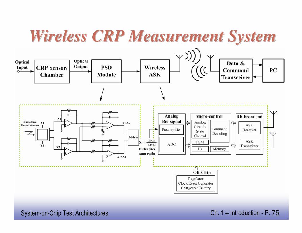
Wireless CRP Measurement SystemWireless CRP Measurement System
EE141System-on-Chip Test Architectures Ch. 1 – Introduction - P. 76
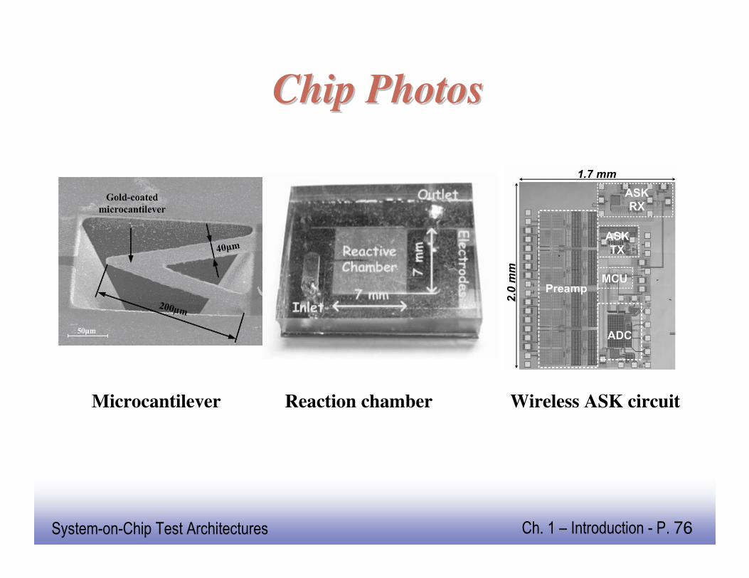
Microcantilever Reaction chamber Wireless ASK circuit
Chip PhotosChip Photos
EE141System-on-Chip Test Architectures Ch. 1 – Introduction - P. 77
Example 2: Network-on-Chip Processor
� Cell processor co-developed by Sony, Toshiba, and IBM [Pham 2005, 2006]:� one Power Processor Element (PPE)
� eight Synergistic Processor Elements (SPEs)
� one Element Interconnection Bus (EIS)
� one Memory Interface Controller (MIC)
� one Bus Interface Controller (BIC)
� one Pervasive Unit (PU)
� one Power Management Unit (PMU)
� one Thermal Management Unit (TMU)
EE141System-on-Chip Test Architectures Ch. 1 – Introduction - P. 78
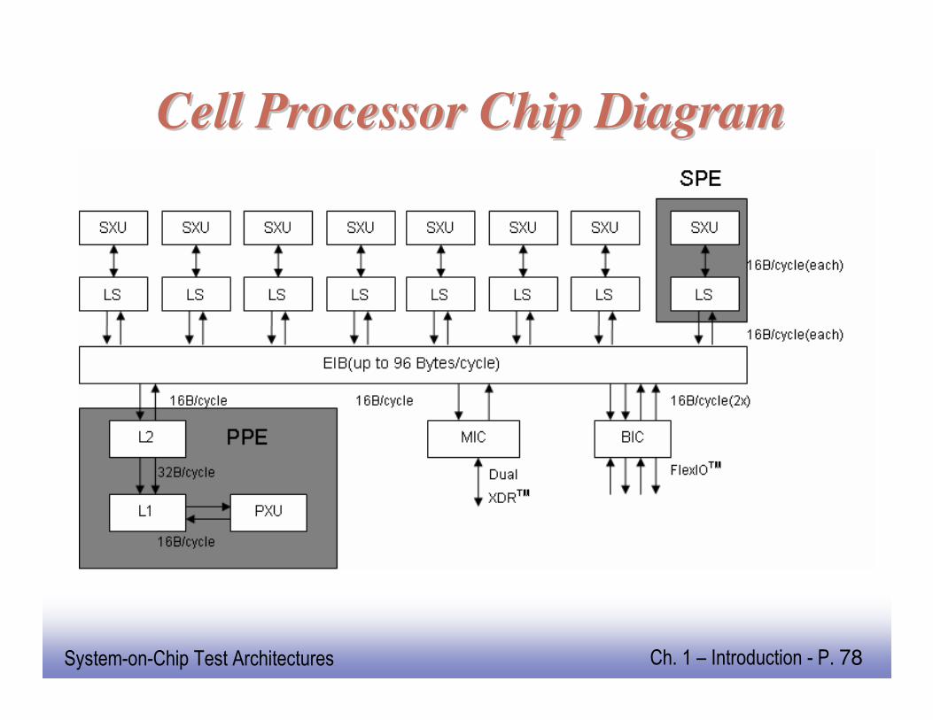
Cell Processor Chip DiagramCell Processor Chip Diagram
EE141System-on-Chip Test Architectures Ch. 1 – Introduction - P. 79
� PU:� Basic chip functions:
– Serial peripheral interface (SPI)
– Phase-locked loop (PLL)– Power-on-reset (POR)
� Lab debug– Fault isolation registers– Performance monitor
(PFM)– Trace logic analyzer (TLA)
� Manufacturing test– Array or Memory BIST– Logic BIST
� PMU and TMU:� Manage chip power to
avoid permanent damage to the chip because of overheating
� PMU – allows software controls to reduce chip power.
� TMU - monitors each of the 10 digital thermal sensors, controls the chip temperature dynamically and interrupts the PPE.
EE141System-on-Chip Test Architectures Ch. 1 – Introduction - P. 80
Section 1.5Section 1.5
About This BookAbout This Book
EE141System-on-Chip Test Architectures Ch. 1 – Introduction - P. 81
About This Book
� DFT Architectures
� New Fault Models and Advanced Techniques
� Yield and Reliability Enhancement
� Nanotechnology Testing Aspects
EE141System-on-Chip Test Architectures Ch. 1 – Introduction - P. 82
DFT Architectures
� Digital Test Architectures (Chapter 2)� Basics of scan testing
� Test compression and logic BIST– Dealing with large scan data for nanometer
designs
� Applying at-speed tests– Crucial for detecting delay faults
EE141System-on-Chip Test Architectures Ch. 1 – Introduction - P. 83
DFT Achitectures
� SOC and NOC (Chapter 4)� Low-cost modular testing of embedded cores
– Providing test access to embedded cores
– Optimizing wrapper designs and test access mechanisms (TAMs)
� Efficient test scheduling
� DFT architectures for network on chips (SOCs)
– Testing interconnect, router, and network interface
EE141System-on-Chip Test Architectures Ch. 1 – Introduction - P. 84
DFT Achitectures
� System-in-Package (SIP) Test Architectures (Chapter 5)� Combination of semiconductors, passives,
and interconnect in single package– Need to test assembly
– May include MEMS and RF components
� Additional test challenges beyond SOCs
EE141System-on-Chip Test Architectures Ch. 1 – Introduction - P. 85
DFT Achitectures
� FPGA Testing (Chapter 12)� Reprogrammability makes attractive for
– Prototyping
– Low-to-moderate volume
– Fast time-to-market
� Testing requires loading multiple configurations
– Time consuming
EE141System-on-Chip Test Architectures Ch. 1 – Introduction - P. 86
DFT Achitectures
� High-Speed I/O Interface (Chapter 14)� Source-synchronous serial links
– Speeds can exceed 1GB/s
– Used on digital systems
� Necessary to test using digital tester for economic reasons
� Describe high-speed I/O test architectures
EE141System-on-Chip Test Architectures Ch. 1 – Introduction - P. 87
DFT Achitectures
� Analog and Mixed-Signal Test Architectures (Chapter 16)� Require very different test techniques from
digital components– Involve specification-based approaches as
opposed to fault-based and defect-based
� Present test architectures for on-chip test and measurement of analog portions
EE141System-on-Chip Test Architectures Ch. 1 – Introduction - P. 88
Fault Models and Advanced
Techniques
� Delay Testing (Chapter 6)� Delay faults prevalent in nanometer
technology– Must detect to achieve high quality
� Describe delay test approaches– New defect-based delay fault models
– Fault simulation
– Test generation
EE141System-on-Chip Test Architectures Ch. 1 – Introduction - P. 89
Fault Models and Advanced
Techniques
� Low-Power Testing (Chapter 7)� Power dissipation during test much higher
than during normal operation– Can result in overheating and “hot spots”
– Ground bounce and power supply droop
– Good part can be failed unnecessarily
� Present low power test techniques– Low-power scan, BIST, and test compression
EE141System-on-Chip Test Architectures Ch. 1 – Introduction - P. 90
Fault Models and Advanced
Techniques
� Coping with Physical Failures, Soft Errors, and Reliability Issues (Chapter 8)� New defect mechanisms in nanometer
technology
� Lower voltage levels and smaller noise margins
– Increased susceptibility to soft errors
� Present techniques for coping with new issues in nanometer technology
EE141System-on-Chip Test Architectures Ch. 1 – Introduction - P. 91
Fault Models and Advanced
Techniques
� Software-Based Self-Testing (Chapter 12)� SOCs typically contain processor(s)
� Software running on processor can perform self-test of SOC
– Reduces amount of DFT circuitry needed
– Provides functional at-speed tests
– Avoids excessive power dissipation
� Present techniques for targeting SOC– Processor itself, memory, global interconnect, and
non-programmable cores
EE141System-on-Chip Test Architectures Ch. 1 – Introduction - P. 92
Fault Models and Advanced
Techniques
� RF Testing (Chapter 16)� Wireless devices increasing prevalent
� RF testing requires different measurement instruments from analog/mixed-signal test
– Noise particularly important factor
� Provide background on RF devices and test methods
EE141System-on-Chip Test Architectures Ch. 1 – Introduction - P. 93
Yield and Reliability
Enhancement
� Fault-Tolerant Design (Chapter 3)� Continue operation in presence of fault
� Require use of redundancy
� Failure rates rising in nanometer SOC designs– Increasingly susceptible to noise
� Review fundamentals of fault-tolerant design– describes many commonly used techniques
EE141System-on-Chip Test Architectures Ch. 1 – Introduction - P. 94
Yield and Reliability
Enhancement
� Design for Manufacturability and Yield (Chapter 9)� DFM involves making layout changes to
improve any aspect of manufacturability– Increasingly important in nanometer technology
� DFY involves techniques targeted towards improving yield
– Coming up with metrics for yield major challenge
� Present examples and discusses issues
EE141System-on-Chip Test Architectures Ch. 1 – Introduction - P. 95
Yield and Reliability
Enhancement
� Design for Debug and Diagnosis (Chapter 10)� Identifying root cause of failure
– Important step for ramping up yield
– Can correct design bugs
– Very time consuming
� Present DFD techniques– Help to rapidly obtain information and speed up
process
EE141System-on-Chip Test Architectures Ch. 1 – Introduction - P. 96
Nanotechnology Testing Aspects
� MEMS Testing (Chapter 13)� Many application areas
– Accelerometers, pressure sensors, micro-optics, inkjet nozzles, optical scanners, etc.
� Describe MEMS devices and discusses test techniques used to characterize
EE141System-on-Chip Test Architectures Ch. 1 – Introduction - P. 97
Nanotechnology Testing Aspects
� Testing Aspects of Nanotechnology Trends (Chapter 17)� Several promising emerging
nanoelectronic technologies– Quantum-dot cellular automata (QCA)
– Carbon nanotube (CNT)
– Hybrid CMOS/Nanowire/Nanodevice (CMOL)
� Describe technologies and research work in developing test techniques