Embed Size (px)
Citation preview

Fundamentals of Power Electronics 1Chapter 11: AC and DC equivalent circuit modelingof the discontinuous conduction mode
Chapter 11AC and DC Equivalent Circuit Modelingof the Discontinuous Conduction Mode
Introduction
11.1. DCM Averaged Switch Model
11.2. Small-Signal AC Modeling of the DCM Switch Network
11.3. High-Frequency Dynamics of Converters in DCM
11.4. Summary of Key Points

Fundamentals of Power Electronics 2Chapter 11: AC and DC equivalent circuit modelingof the discontinuous conduction mode
We are missing ac and dc equivalent circuit modelsfor the discontinuous conduction mode
DC
CCM
DCM
+–
1 : M(D)
Vg R
+
V
–
+–Vg R
+
V
–
+–
+– 1 : M(D) Le
C R
+
–
v(s)
e(s) d(s)
j(s) d(s)
AC
+– Rvg(s)
+
–
v(s)
vg(s)
??

Fundamentals of Power Electronics 3Chapter 11: AC and DC equivalent circuit modelingof the discontinuous conduction mode
Change in characteristics at the CCM/DCM boundary
l Steady-state output voltage becomes strongly load-dependentl Simpler dynamics: one pole and the RHP zero are moved to very high
frequency, and can normally be ignored
l Traditionally, boost and buck-boost converters are designed to operatein DCM at full load
l All converters may operate in DCM at light load
So we need equivalent circuits that model the steady-state and small-signal ac models of converters operating in DCM
The averaged switch approach will be employed

Fundamentals of Power Electronics 4Chapter 11: AC and DC equivalent circuit modelingof the discontinuous conduction mode
11.1 Derivation of DCM averaged switch model:buck-boost example
+–
L
C R
+
v
–
vg
iL
+vL–
Switch network
+
v1
–
–
v2
+
i1 i2• Define switch terminalquantities v1, i1, v2, i2, asshown
• Let us find the averagedquantities ⟨ v1 ⟩, ⟨ i1 ⟩ , ⟨ v2 ⟩,⟨ i2 ⟩, for operation in DCM,and determine therelations between them

Fundamentals of Power Electronics 5Chapter 11: AC and DC equivalent circuit modelingof the discontinuous conduction mode
d1Ts
Ts
t
i1(t)ipkArea q1
i1(t) Ts
v1(t)
0
vg – v
v1(t) Tsvg
i2(t)ipk Area q2
v2(t)
0
vg – v
– v
i2(t) Ts
v2(t) Ts
d2Ts d3Ts
DCM waveforms
t
iL(t)
0
ipk
vg
L
vL
vL(t) vg
v
0
+–
L
C R
+
v
–
vg
iL
+vL–
Switch network
+
v1
–
–
v2
+
i1 i2

Fundamentals of Power Electronics 6Chapter 11: AC and DC equivalent circuit modelingof the discontinuous conduction mode
Basic DCM equations:ipk, vL, and d2 (Approximate method)
d1Ts
Ts
t
i1(t)ipkArea q1
i1(t) Ts
v1(t)
0
vg – v
v1(t) Tsvg
i2(t)ipk Area q2
v2(t)
0
vg – v
– v
i2(t) Ts
v2(t) Ts
d2Ts d3Ts
ipk =vg
Ld1Ts
vL(t) Ts= d1 vg(t) Ts
+ d2 v(t)Ts
+ d3 ⋅ 0
Peak inductor current:
Average inductor voltage:
In DCM, the diode switches off when theinductor current reaches zero. Hence, i(0)= i(Ts) = 0, and the average inductorvoltage is zero. This is true even duringtransients.
vL(t) Ts= d1(t) vg(t) Ts
+ d2(t) v(t)Ts
= 0
Solve for d2:
d2(t) = – d1(t)vg(t) Ts
v(t)Ts

Fundamentals of Power Electronics 7Chapter 11: AC and DC equivalent circuit modelingof the discontinuous conduction mode
Average switch network terminal voltages
d1Ts
Ts
t
i1(t)ipkArea q1
i1(t) Ts
v1(t)
0
vg – v
v1(t) Tsvg
i2(t)ipk Area q2
v2(t)
0
vg – v
– v
i2(t) Ts
v2(t) Ts
d2Ts d3Ts
Average the v1(t) waveform:
v1(t) Ts= d1(t) ⋅ 0 + d2(t) vg(t) Ts
– v(t)Ts
+ d3(t) vg(t) Ts
Eliminate d2 and d3:
v1(t) Ts= vg(t) Ts
Similar analysis for v2(t) waveform leads to
v2(t) Ts= d1(t) vg(t) Ts
– v(t)Ts
+ d2(t) ⋅ 0 + d3(t) – v(t)Ts
= – v(t)Ts

Fundamentals of Power Electronics 8Chapter 11: AC and DC equivalent circuit modelingof the discontinuous conduction mode
Average switch network terminal currents
d1Ts
Ts
t
i1(t)ipkArea q1
i1(t) Ts
v1(t)
0
vg – v
v1(t) Tsvg
i2(t)ipk Area q2
v2(t)
0
vg – v
– v
i2(t) Ts
v2(t) Ts
d2Ts d3Ts
Average the i1(t) waveform:
Eliminate ipk:
Note ⟨ i1(t)⟩Ts is not equal to d ⟨ iL(t)⟩Ts !
Similar analysis for i2(t) waveform leads to
i1(t) Ts= 1
Tsi1(t)dt
t
t + Ts
=q1
Ts
The integral q1 is the area under the i1(t)waveform during first subinterval. Use trianglearea formula:
q1 = i1(t)dtt
t + Ts
= 12
d1Ts ipk
i1(t) Ts=
d 12(t) Ts
2Lv1(t) Ts
i2(t) Ts=
d 12(t) Ts
2L
v1(t) Ts
2
v2(t) Ts

Fundamentals of Power Electronics 9Chapter 11: AC and DC equivalent circuit modelingof the discontinuous conduction mode
Input port: Averaged equivalent circuit
i1(t) Ts=
d 12(t) Ts
2Lv1(t) Ts
i1(t) Ts=
v1(t) Ts
Re(d1)
Re(d1) = 2Ld 1
2 Ts
v1(t) Ts
i1(t) Ts
Re(d1)
+
–

Fundamentals of Power Electronics 10Chapter 11: AC and DC equivalent circuit modelingof the discontinuous conduction mode
Output port: Averaged equivalent circuit
i2(t) Ts=
d 12(t) Ts
2L
v1(t) Ts
2
v2(t) Ts
i2(t) Tsv2(t) Ts
=v1(t) Ts
2
Re(d1)= p(t)
Ts
p(t)
+
v(t)
–
i(t)

Fundamentals of Power Electronics 11Chapter 11: AC and DC equivalent circuit modelingof the discontinuous conduction mode
The dependent power source
p(t)
+
v(t)
–
i(t)
v(t)i(t) = p(t)
v(t)
i(t)
• Must avoid open- and short-circuitconnections of power sources
• Power sink: negative p(t)

Fundamentals of Power Electronics 12Chapter 11: AC and DC equivalent circuit modelingof the discontinuous conduction mode
How the power source arisesin lossless two-port networks
In a lossless two-port network without internal energy storage:instantaneous input power is equal to instantaneous output power
In all but a small number of special cases, the instantaneous powerthroughput is dependent on the applied external source and load
If the instantaneous power depends only on the external elementsconnected to one port, then the power is not dependent on thecharacteristics of the elements connected to the other port. The otherport becomes a source of power, equal to the power flowing throughthe first port
A power source (or power sink) element is obtained

Fundamentals of Power Electronics 13Chapter 11: AC and DC equivalent circuit modelingof the discontinuous conduction mode
Properties of power sources
P1
P2 P3
P1 + P2 + P3
P1P1
n1 : n2
Series and parallelconnection of powersources
Reflection of powersource through atransformer

Fundamentals of Power Electronics 14Chapter 11: AC and DC equivalent circuit modelingof the discontinuous conduction mode
The loss-free resistor (LFR)
i2(t) Ts
+
–
v2(t) Tsv1(t) Ts
i1(t) Ts
Re(d1)
+
–
p(t)Ts
A two-port lossless network
Input port obeys Ohm’s Law
Power entering input port is transferred to output port

Fundamentals of Power Electronics 15Chapter 11: AC and DC equivalent circuit modelingof the discontinuous conduction mode
Averaged modeling of CCM and DCM switch networks
+
–
1 : d(t)i1(t) Tsi2(t) Ts
+
–
v2(t) Tsv1(t) Ts
Averaged switch modelSwitch network
CCM
+
v2(t)
–
+
v1(t)
–
i1(t) i2(t)
i2(t) Ts
+
–
v2(t) Tsv1(t) Ts
i1(t) Ts
Re(d1)
+
–
DCM
+
v2(t)
–
+
v1(t)
–
i1(t) i2(t)p(t)
Ts

Fundamentals of Power Electronics 16Chapter 11: AC and DC equivalent circuit modelingof the discontinuous conduction mode
Averaged switch model: buck-boost example
+–
L
C R
+
v
–
vg
iL
+vL–
Switch network
+
v1
–
–
v2
+
i1 i2
i2(t) Ts
v2(t) Tsv1(t) Ts
i1(t) Ts
Re(d)
+–
L
C R
+
–
+
–
–
+ v(t)Ts
vg(t) Ts
p(t)Ts
Original circuit
Averaged model

Fundamentals of Power Electronics 17Chapter 11: AC and DC equivalent circuit modelingof the discontinuous conduction mode
Solution of averaged model: steady state
P
Re(D)+– R
+
V
–
Vg
I1Let
L → short circuit
C → open circuit
Converter input power:
Converter output power:
Equate and solve:P =
V g2
Re
P = V 2
R
P =V g
2
Re= V 2
R
VVg
= ± RRe

Fundamentals of Power Electronics 18Chapter 11: AC and DC equivalent circuit modelingof the discontinuous conduction mode
Steady-state LFR solution
VVg
= ± RRe
is a general result, for any system that canbe modeled as an LFR.
For the buck-boost converter, we have
Re(D) = 2LD2Ts
Eliminate Re:
VVg
= –D2TsR
2L= – D
K
which agrees with the previous steady-state solution of Chapter 5.

Fundamentals of Power Electronics 19Chapter 11: AC and DC equivalent circuit modelingof the discontinuous conduction mode
Steady-state LFR solution with ac terminal waveforms
p(t)Re
+– R
+
v(t)
–
vg(t)
i1(t) i2(t)
C
Converter average inputpower:
Converter average outputpower:
Equate and solve:Pav =
V g,rms2
Re
Pav =V rms
2
R
Vrms
Vg,rms= R
Re
Note that no average powerflows into capacitor

Fundamentals of Power Electronics 20Chapter 11: AC and DC equivalent circuit modelingof the discontinuous conduction mode
Averaged models of other DCM converters
• Determine averaged terminal waveforms of switch network
• In each case, averaged transistor waveforms obey Ohm’s law, whileaveraged diode waveforms behave as dependent power source
• Can simply replace transistor and diode with the averaged model asfollows:
i2(t) Ts
+
–
v2(t) Tsv1(t) Ts
i1(t) Ts
Re(d1)
+
–
+
v2(t)
–
+
v1(t)
–
i1(t) i2(t)p(t)
Ts

Fundamentals of Power Electronics 21Chapter 11: AC and DC equivalent circuit modelingof the discontinuous conduction mode
DCM buck, boost
Re(d)
+–
L
C R
+
–
v(t)Ts
vg(t) Ts
Re(d)+–
L
C R
+
–
v(t)Ts
vg(t) Ts
Buck
Boost
p(t)Ts
p(t)Ts
Re = 2Ld 2Ts

Fundamentals of Power Electronics 22Chapter 11: AC and DC equivalent circuit modelingof the discontinuous conduction mode
DCM Cuk, SEPIC
Cuk
+–
L1
C2 R
C1 L2
vg(t) Ts
+
–
v(t)TsRe(d)
+–
L1
C2 R
C1
L2vg(t) Ts
+
–
v(t)TsRe(d)
SEPIC
p(t)Ts
p(t)Ts
Re =2 L1||L2
d 2Ts

Fundamentals of Power Electronics 23Chapter 11: AC and DC equivalent circuit modelingof the discontinuous conduction mode
Steady-state solution: DCM buck, boost
P
Re(D)
+– R
+
V
–
Vg
PRe(D)+– R
+
V
–
Vg
Let L → short circuit
C → open circuit
Buck
Boost

Fundamentals of Power Electronics 24Chapter 11: AC and DC equivalent circuit modelingof the discontinuous conduction mode
Steady-state solution of DCM/LFR models
Table 11.1. CCM and DCM conversion ratios of basic converters
Converter M, CCM M, DCM
Buck D 21 + 1 + 4Re/R
Boost 11 – D 1 + 1 + 4R/Re
2
Buck-boost, Cuk – D1 – D
– RRe
SEPIC D1 – D
RRe
I > Icrit for CCMI < Icrit for DCM
Icrit = 1 – DD
Vg
Re(D)

Fundamentals of Power Electronics 25Chapter 11: AC and DC equivalent circuit modelingof the discontinuous conduction mode
11.2 Small-signal ac modeling of the DCM switch network
d(t) = D + d(t)
v1(t) Ts= V1 + v1(t)
i1(t) Ts= I1 + i1(t)
v2(t) Ts= V2 + v2(t)
i2(t) Ts= I2 + i2(t)
i2(t) Ts
+
–
v2(t) Tsv1(t) Ts
i1(t) Ts
Re(d)
+
–
p(t)Ts
d(t)
Large-signal averaged model Perturb and linearize: let
i1(t) Ts=
d 12(t) Ts
2Lv1(t) Ts
i2(t) Ts=
d 12(t) Ts
2L
v1(t) Ts
2
v2(t) Ts
i1 =v1r1
+ j1d + g1v2
i2 = –v2r2
+ j2d + g2v1

Fundamentals of Power Electronics 26Chapter 11: AC and DC equivalent circuit modelingof the discontinuous conduction mode
Linearization via Taylor series
i1(t) Ts=
v1(t) Ts
Re(d(t))= f1 v1(t) Ts
, v2(t) Ts, d(t)
I1 + i1(t) = f1 V1, V2, D + v1(t)d f1 v1, V2, D
dv1 v1 = V1
+ v2(t)d f1 V1, v2, D
dv2 v2 = V2
+ d(t)d f1 V1, V2, d
dd d = D
+ higher–order nonlinear terms
Given the nonlinear equation
Expand in three-dimensional Taylor series about the quiescentoperating point: (for simple
notation,drop anglebrackets)

Fundamentals of Power Electronics 27Chapter 11: AC and DC equivalent circuit modelingof the discontinuous conduction mode
Equate dc and first-order ac terms
I1 = f1 V1, V2, D =V1
Re(D)i1(t) = v1(t)1r1
+ v2(t) g1 + d(t) j1
1r1
=d f1 v1, V2, D
dv1 v1 = V1
= 1Re(D)
g1 =d f1 V1, v2, D
dv2 v2 = V2
= 0
j1 =d f1 V1, V2, d
dd d = D= –
V1
Re2(D)
dRe(d)dd d = D
=2V1
DRe(D)
AC DC

Fundamentals of Power Electronics 28Chapter 11: AC and DC equivalent circuit modelingof the discontinuous conduction mode
Output portsame approach
i2(t) Ts=
v1(t) Ts
2
Re(d(t)) v2(t) Ts
= f2 v1(t) Ts, v2(t) Ts
, d(t)
I2 = f2 V1, V2, D =V 1
2
Re(D) V2
i2(t) = v2(t) – 1r2
+ v1(t)g2 + d(t) j2
DC terms
Small-signal aclinearization

Fundamentals of Power Electronics 29Chapter 11: AC and DC equivalent circuit modelingof the discontinuous conduction mode
Output resistance parameter r2
1r2
= –d f2 V1, v2, D
dv2 v2 = V2
= 1R = 1
M 2 Re(D)
Loadcharacteristic
– 1r2
v2(t) Ts
i2(t) Ts
1R
Quiescentoperating
point
Power sourcecharacteristic
Linearizedmodel

Fundamentals of Power Electronics 30Chapter 11: AC and DC equivalent circuit modelingof the discontinuous conduction mode
Small-signal DCM switch model parameters
–
+
+–v1 r1 j1d g1v2
i1
g2v1 j2d r2
i2
v2
Tabl e 11.2. Small -signal DCM switch model parameters
Switch type g1 j1 r1 g2 j2 r2
Buck,Fig. 11.16(a)
1Re
2(1 – M)V1
DRe
Re 2 – MMRe
2(1 – M)V1
DMRe
M 2Re
Boost,Fig. 11.16(b)
1(M – 1)2 Re
2MV1
D(M – 1)Re
(M – 1)2
MRe
2M – 1(M – 1)2 Re
2V1
D(M – 1)Re
(M – 1)2Re
Gen two-switchFig. 11.7(a)
0 2V1
DRe
Re 2M
Re 2V1
DMRe
M 2Re

Fundamentals of Power Electronics 31Chapter 11: AC and DC equivalent circuit modelingof the discontinuous conduction mode
Small-signal ac model, DCM buck-boost example
+
–
+–
v1 r1 j1d g1v2
i1
g2v1 j2d r2
i2
v2
–
+
L
C R
Switch network small-signal ac model
+
–vg v
iL

Fundamentals of Power Electronics 32Chapter 11: AC and DC equivalent circuit modelingof the discontinuous conduction mode
A more convenient way to model the buck and boostsmall-signal DCM switch networks
+
v2(t)
–
i1(t) i2(t)
+
v1(t)
–
+
v2(t)
–
i1(t) i2(t)
+
v1(t)
–
+
–
+
–
v1 r1 j1d g1v2
i1
g2v1 j2d r2
i2
v2
In any event, a small-signal two-port model is used, of the form

Fundamentals of Power Electronics 33Chapter 11: AC and DC equivalent circuit modelingof the discontinuous conduction mode
Small-signal ac models of the DCM buck and boostconverters (more convenient forms)
+
–
+– v1 r1 j1d g1v2
i1
g2v1 j2d r2
i2
v2
+
–
L
C R
DCM buck switch network small-signal ac model
+
–
vg v
iL
+
–
+– v1 r1 j1d g1v2
i1
g2v1 j2d r2
i2
v2
+
–
L
C R
DCM boost switch network small-signal ac model
+
–
vg v
iL

Fundamentals of Power Electronics 34Chapter 11: AC and DC equivalent circuit modelingof the discontinuous conduction mode
DCM small-signal transfer functions
l When expressed in terms of R, L, C, and M (not D), the small-signal transfer functions are the same in DCM as in CCM
l Hence, DCM boost and buck-boost converters exhibit two polesand one RHP zero in control-to-output transfer functions
l But , value of L is small in DCM. Hence
RHP zero appears at high frequency, usually greater thanswitching frequency
Pole due to inductor dynamics appears at high frequency, nearto or greater than switching frequency
So DCM buck, boost, and buck-boost converters exhibitessentially a single-pole response
l A simple approximation: let L → 0

Fundamentals of Power Electronics 35Chapter 11: AC and DC equivalent circuit modelingof the discontinuous conduction mode
The simple approximation L → 0
Buck, boost, and buck-boost converter models all reduce to
+
–
+– r1 j1d g1v2 g2v1 j2d r2 C R
DCM switch network small-signal ac model
vg v
Transfer functions
Gvd(s) =v
dvg = 0
=Gd0
1 + sωp
Gd0 = j2 R || r2
ωp = 1R || r2 C
Gvg(s) =v
vg d = 0
=Gg0
1 + sωp
Gg0 = g2 R || r2 = M
withcontrol-to-output
line-to-output

Fundamentals of Power Electronics 36Chapter 11: AC and DC equivalent circuit modelingof the discontinuous conduction mode
Transfer function salient features
Tabl e 11.3. Salient features of DCM converter small -signal transfer functions
Converter Gd0 Gg0 ωp
Buck 2VD
1 – M2 – M M 2 – M
(1 – M)RC
Boost 2VD
M – 12M – 1 M 2M – 1
(M– 1)RC
Buck-boost VD M 2
RC

Fundamentals of Power Electronics 37Chapter 11: AC and DC equivalent circuit modelingof the discontinuous conduction mode
DCM boost example
R = 12 Ω
L = 5 µH
C = 470 µF
fs = 100 kHz
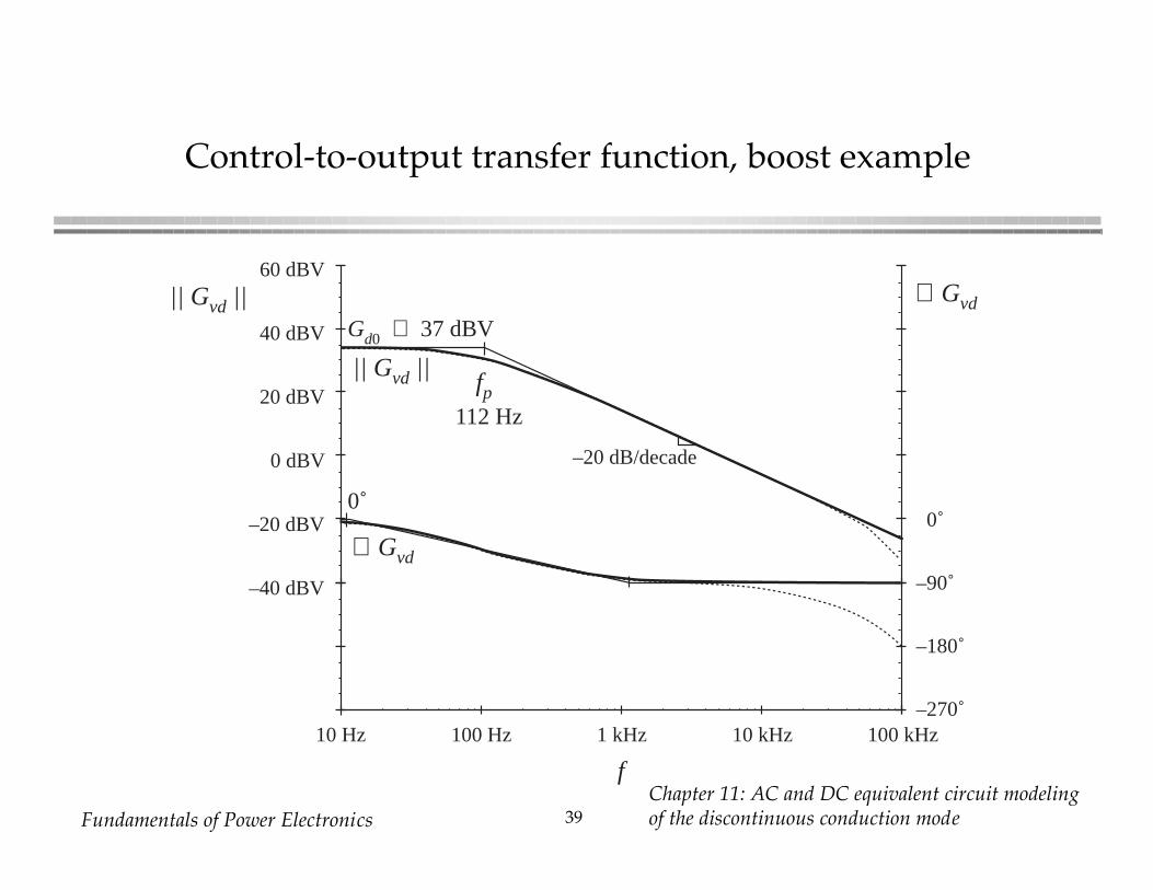
The output voltage is regulated to be V = 36 V. It is desired to determine Gvd(s) at the
operating point where the load current is I = 3 A and the dc input voltage is Vg = 24 V.

Fundamentals of Power Electronics 38Chapter 11: AC and DC equivalent circuit modelingof the discontinuous conduction mode
Evaluate simple model parameters
P = I V – Vg = 3 A 36 V – 24 V = 36 W
Re =V g
2
P=
(24 V)2
36 W= 16 Ω
D = 2LReTs
=2(5 µH)
(16 Ω)(10 µs)= 0.25
Gd0 = 2VD
M – 12M – 1
=2(36 V)(0.25)
(36 V)(24 V)
– 1
2(36 V)(24 V)
– 1
= 72 V ⇒ 37 dBV
fp =ωp
2π = 2M – 12π(M– 1)RC
=
2(36 V)(24 V)
– 1
2π (36 V)(24 V)
– 1 (12 Ω)(470 µF)= 112 Hz
Fundamentals of Power Electronics 39Chapter 11: AC and DC equivalent circuit modelingof the discontinuous conduction mode
Control-to-output transfer function, boost example
–20 dB/decade
fp112 Hz
Gd0 ⇒ 37 dBV
f
0˚0˚
–90˚
–180˚
–270˚
|| Gvd ||
|| Gvd || ∠ Gvd
0 dBV
–20 dBV
–40 dBV
20 dBV
40 dBV
60 dBV
∠ Gvd
10 Hz 100 Hz 1 kHz 10 kHz 100 kHz

Fundamentals of Power Electronics 40Chapter 11: AC and DC equivalent circuit modelingof the discontinuous conduction mode
11.4 Summary of Key Points
1. In the discontinuous conduction mode, the average transistor voltageand current are proportional, and hence obey Ohm’s law. Anaveraged equivalent circuit can be obtained by replacing thetransistor with an effective resistor Re(d). The average diode voltageand current obey a power source characteristic, with power equal tothe power effectively dissipated by Re. In the averaged equivalentcircuit, the diode is replaced with a dependent power source.
2. The two-port lossless network consisting of an effective resistor andpower source, which results from averaging the transistor and diodewaveforms of DCM converters, is called a loss-free resistor. Thisnetwork models the basic power-processing functions of DCMconverters, much in the same way that the ideal dc transformermodels the basic functions of CCM converters.
3. The large-signal averaged model can be solved under equilibriumconditions to determine the quiescent values of the converter currentsand voltages. Average power arguments can often be used.

Fundamentals of Power Electronics 41Chapter 11: AC and DC equivalent circuit modelingof the discontinuous conduction mode
Key points
4. A small-signal ac model for the DCM switch network can bederived by perturbing and linearizing the loss-free resistornetwork. The result has the form of a two-port y-parameter model.The model describes the small-signal variations in the transistorand diode currents, as functions of variations in the duty cycle andin the transistor and diode ac voltage variations. This model ismost convenient for ac analysis of the buck-boost converter.
5. To simplify the ac analysis of the DCM buck and boost converters,it is convenient to define two other forms of the small-signalswitch model, corresponding to the switch networks of Figs.10.16(a) and 10.16(b). These models are also y-parameter two-port models, but have different parameter values.

Fundamentals of Power Electronics 42Chapter 11: AC and DC equivalent circuit modelingof the discontinuous conduction mode
Key points
6. Since the inductor value is small when the converter operates inthe discontinuous conduction mode, the inductor dynamics of theDCM buck, boost, and buck-boost converters occur at highfrequency, above or just below the switching frequency. Hence, inmost cases the inductor dynamics can be ignored. In the small-signal ac model, the inductance L is set to zero, and theremaining model is solved relatively easily for the low-frequencyconverter dynamics. The DCM buck, boost, and buck-boostconverters exhibit transfer functions containing a single low-frequency dominant pole.
7. It is also possible to adapt the CCM models developed in Chapter 7to treat converters with switches that operate in DCM, as well asother switches discussed in later chapters. The switch conversionratio µ is a generalization of the duty cycle d of CCM switchnetworks; this quantity can be substituted in place of d in anyCCM model. The result is a model that is valid for DCM operation.Hence, existing CCM models can be adapted directly.

Fundamentals of Power Electronics 43Chapter 11: AC and DC equivalent circuit modelingof the discontinuous conduction mode
Key points
8. The conversion ratio µ of DCM switch networks is a function of theapplied voltage and current. As a result, the switch networkcontains effective feedback. So the small-signal model of a DCMconverter can be expressed as the CCM converter model, pluseffective feedback representing the behavior of the DCM switchnetwork. Two effects of this feedback are increase of theconverter output impedance via current feedback, and decreaseof the Q-factor of the transfer function poles. The pole arising fromthe inductor dynamics occurs at the crossover frequency of theeffective current feedback loop.