Embed Size (px)
Citation preview
CHAPTER 16 PHOTODETECTION
Abhay M . Joshi Disco y ery Semiconductors , Inc . Cranbury , New Jersey
Gregory H . Olsen Sensors Unlimited , Inc . Princeton , New Jersey
1 6 . 1 GLOSSARY
A photodetector active area A 0 incident photon flux B bandwidth of the photodetector C capacitance of the photodetector
D * detectivity E applied electric field
E a activation energy E g bandgap of the semiconductor E i impurity energy state
f frequency I dif f dif fusion current I g - r generation-recombination current
IR 0 unity gain current IR 1 reverse current generated by avalanche action
I t u n tunneling current k Boltzmann’s constant
L distance traveled by a charge carrier M photocurrent gain
m ef fective mass of electrons N A acceptor impurity concentration on p side
N D donor impurity concentration on n side n refractive index of the AR coating
q electron charge
16 .1
16 .2 OPTICAL DETECTORS
R sum of the detector series resistance and load resistance R o detector shunt impedance T temperature in degrees Kelvin t n transit time of electrons t p transit time of holes t r transit time of charge carriers (holes or electrons) V applied reverse bias in volts
V B breakdown voltage V b i built-in potential of a p - n junction
W depletion width of a p - n junction a absorption coef ficient of the photodetector’s absorption layer
» s semiconductor permittivity h quantum ef ficiency of photodetector
θ tunneling constant l wavelength of incident photons (nm)
l c o detector cutof f wavelength (10 percent of peak response , nm) m mobility of charge carriers (holes or electrons)
m n mobility of electrons m p mobility of holes
1 6 . 2 INTRODUCTION
The approach of this chapter will be descriptive and tutorial rather than encyclopedic . It is assumed that the reader is primarily interested in an overview of how things work . Among the many excellent references to be consulted for further details are Sze’s book , 1 and the article by Forrest . 2 For the latest in photodetector developments , consult recent proceed- ings of the Society of Photo-optical and Instrumentation Engineers (SPIE) conference or the IEEE Optical Fiber Conference .
A photodetector is a solid-state sensor that converts light energy into electrical energy . According to Isaac Newton , light energy consists of small packets or bundles of particles called photons . Albert Einstein , who won a Nobel prize for the discovery of the photoelectric ef fect , showed that when these photons hit a metal they could excite electrons in it . The minimum photo energy required to generate (excite) an electron is defined as the work function and the number of electrons generated is proportional to the intensity of the light . The semiconductor photodetectors are made from dif ferent semiconductor materials such as silicon , germanium , indium gallium arsenide , indium antimonide , and mercury cadmium telluride , to name a few . Each material has a characteristic bandgap energy ( E g ) which determines its light-absorbing capabilities . Light is a form of electromagnetic radiation comprised of dif ferent wavelengths ( l ) . The range of light spectrum is split approximately as : ultraviolet (0 – 400 nm) ; visible (400 – 1000 nm) ; near infrared (1000 – 3000 nm) ; medium infrared (3000 – 6000 nm) ; far infrared (6000 – 40 , 000 nm) ; extreme infrared (40 , 000 – 100 , 000 nm) . The equation between bandgap energy ( E g ) and cutof f wavelength ( l c ) is
l c 5 1 . 24 3 10 3 nm
E g (eV) (1)
PHOTODETECTION 16 .3
TABLE 1 Important Photodetector Materials
Type E g (eV) l c (nm) Band
Silicon Gallium arsenide Germanium Indium gallium arsenide* Indium arsenide Indium antimonide Mercury cadmium
1 . 12 1 . 42 0 . 66
0 . 73 – 0 . 47 0 . 36 0 . 17
0 . 7 – 0 . 1
1100 875
1800 1700 – 2600
3400 5700
1700 – 12500
Visible Visible Near-infrared Near-infrared Near-infrared Medium-infrared Near-to-far-infrared
* The alloy composition of indium gallium arsenide and mercury cadmium telluride can be changed to alter the bandgap ( E g ) .
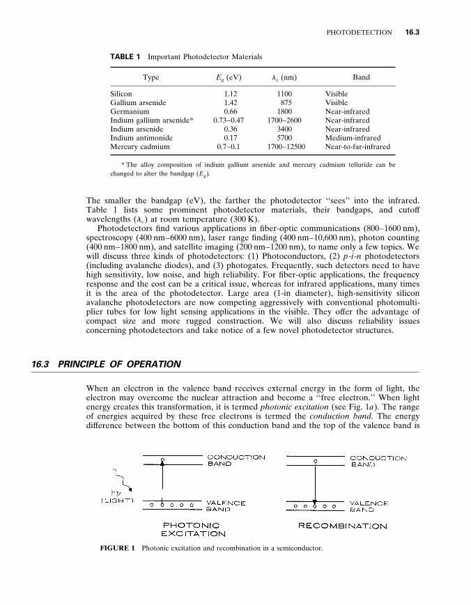
The smaller the bandgap (eV) , the farther the photodetector ‘‘sees’’ into the infrared . Table 1 lists some prominent photodetector materials , their bandgaps , and cutof f wavelengths ( l c ) at room temperature (300 K) .
Photodetectors find various applications in fiber-optic communications (800 – 1600 nm) , spectroscopy (400 nm – 6000 nm) , laser range finding (400 nm – 10 , 600 nm) , photon counting (400 nm – 1800 nm) , and satellite imaging (200 nm – 1200 nm) , to name only a few topics . We will discuss three kinds of photodetectors : (1) Photoconductors , (2) p - i - n photodetectors (including avalanche diodes) , and (3) photogates . Frequently , such detectors need to have high sensitivity , low noise , and high reliability . For fiber-optic applications , the frequency response and the cost can be a critical issue , whereas for infrared applications , many times it is the area of the photodetector . Large area (1-in diameter) , high-sensitivity silicon avalanche photodetectors are now competing aggressively with conventional photomulti- plier tubes for low light sensing applications in the visible . They of fer the advantage of compact size and more rugged construction . We will also discuss reliability issues concerning photodetectors and take notice of a few novel photodetector structures .
1 6 . 3 PRINCIPLE OF OPERATION
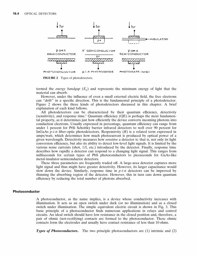
When an electron in the valence band receives external energy in the form of light , the electron may overcome the nuclear attraction and become a ‘‘free electron . ’’ When light energy creates this transformation , it is termed photonic excitation (see Fig . 1 a ) . The range of energies acquired by these free electrons is termed the conduction band . The energy dif ference between the bottom of this conduction band and the top of the valence band is
FIGURE 1 Photonic excitation and recombination in a semiconductor .
16 .4 OPTICAL DETECTORS
FIGURE 2 Types of photodetectors .
termed the energy bandgap ( E g ) and represents the minimum energy of light that the material can absorb .
However , under the influence of even a small external electric field , the free electrons can ‘‘drift’’ in a specific direction . This is the fundamental principle of a photodetector . Figure 2 shows the three kinds of photodetectors discussed in this chapter . A brief explanation of each kind follows .
All photodetectors can be characterized by their quantum ef ficiency , detectivity (sensitivity) , and response time . 1 Quantum ef ficiency (QE) is perhaps the most fundamen- tal property , as it determines just how ef ficiently the device converts incoming photons into conduction electrons . Usually expressed in percentage , quantum ef ficiency can range from under 1 percent for PtSi Schottky barrier infrared detectors to well over 90 percent for InGaAs p - i - n fiber-optic photodetectors . Responsivity ( R ) is a related term expressed in amps / watt , which determines how much photocurrent is produced by optical power of a given wavelength . Detectivity measures how sensiti y e a detector is : that is , not only its light conversion ef ficiency , but also its ability to detect low-level light signals . It is limited by the various noise currents (shot , 1 / f , etc . ) introduced by the detector . Finally , response time describes how rapidly a detector can respond to a changing light signal . This ranges from milliseconds for certain types of PbS photoconductors to picoseconds for GaAs-like metal-insulator-semiconductor detectors .
These three parameters are frequently traded of f . A large-area detector captures more light signal and thus might have greater detectivity . However , its larger capacitance would slow down the device . Similarly , response time in p - i - n detectors can be improved by thinning the absorbing region of the detector . However , this in turn cuts down quantum ef ficiency by reducing the total number of photons absorbed .
Photoconductor
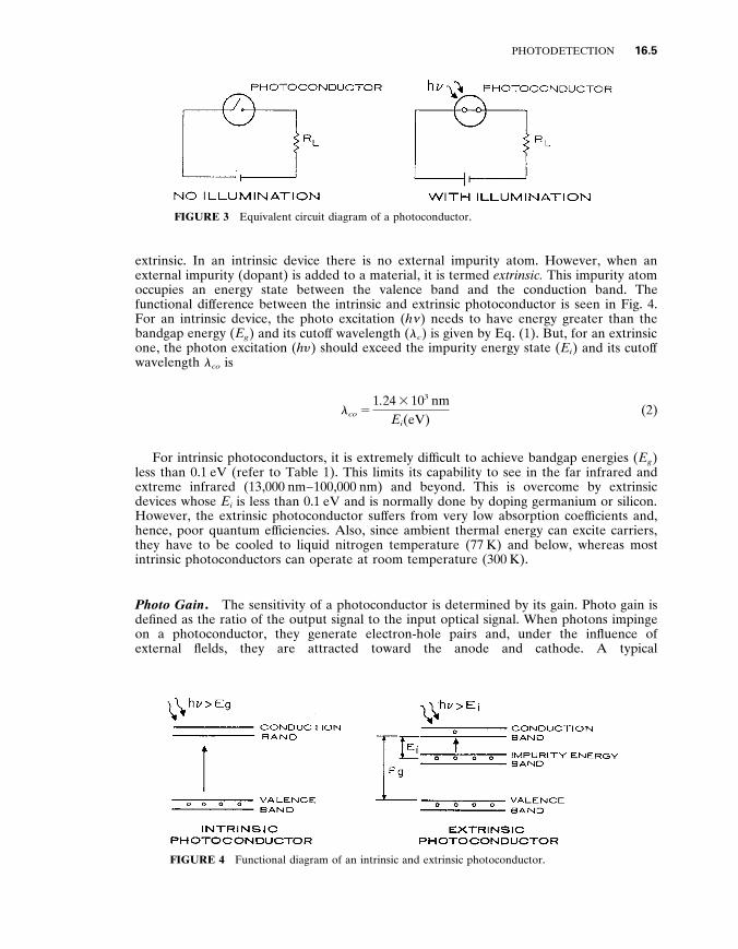
A photoconductor , as the name implies , is a device whose conductivity increases with illumination . It acts as an open switch under dark (or no illumination) and as a closed switch under illumination . The simple equivalent electric circuit is shown in Fig . 3 . This basic principle of a photoconductor finds numerous applications in relays and control circuits . An ideal switch should have low resistance in the closed position and , therefore , a pair of ohmic (not-rectifying) contacts are formed to the photoconductor . These ohmic contacts form the electrodes and usually have contact resistance of less than 10 ohms .
Types of Photoconductors . The two principle photoconductors are (1) intrinsic and (2)
PHOTODETECTION 16 .5
FIGURE 3 Equivalent circuit diagram of a photoconductor .
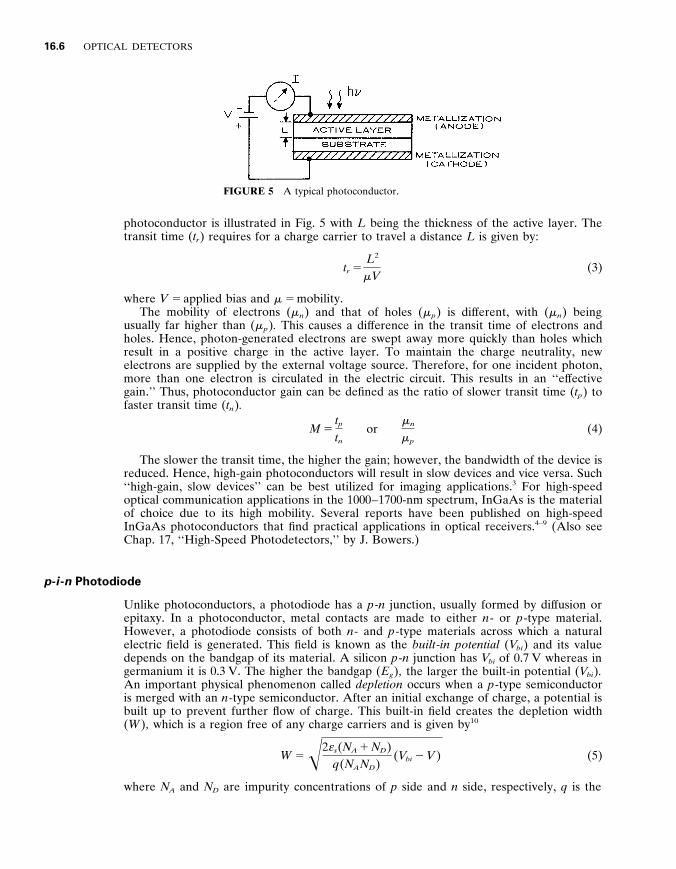
extrinsic . In an intrinsic device there is no external impurity atom . However , when an external impurity (dopant) is added to a material , it is termed extrinsic . This impurity atom occupies an energy state between the valence band and the conduction band . The functional dif ference between the intrinsic and extrinsic photoconductor is seen in Fig . 4 . For an intrinsic device , the photo excitation ( h … ) needs to have energy greater than the bandgap energy ( E g ) and its cutof f wavelength ( l c ) is given by Eq . (1) . But , for an extrinsic one , the photon excitation ( h y ) should exceed the impurity energy state ( E i ) and its cutof f wavelength l c o is
l c o 5 1 . 24 3 10 3 nm
E i (eV) (2)
For intrinsic photoconductors , it is extremely dif ficult to achieve bandgap energies ( E g ) less than 0 . 1 eV (refer to Table 1) . This limits its capability to see in the far infrared and extreme infrared (13 , 000 nm – 100 , 000 nm) and beyond . This is overcome by extrinsic devices whose E i is less than 0 . 1 eV and is normally done by doping germanium or silicon . However , the extrinsic photoconductor suf fers from very low absorption coef ficients and , hence , poor quantum ef ficiencies . Also , since ambient thermal energy can excite carriers , they have to be cooled to liquid nitrogen temperature (77 K) and below , whereas most intrinsic photoconductors can operate at room temperature (300 K) .
Photo Gain . The sensitivity of a photoconductor is determined by its gain . Photo gain is defined as the ratio of the output signal to the input optical signal . When photons impinge on a photoconductor , they generate electron-hole pairs and , under the influence of external flelds , they are attracted toward the anode and cathode . A typical
FIGURE 4 Functional diagram of an intrinsic and extrinsic photoconductor .
16 .6 OPTICAL DETECTORS
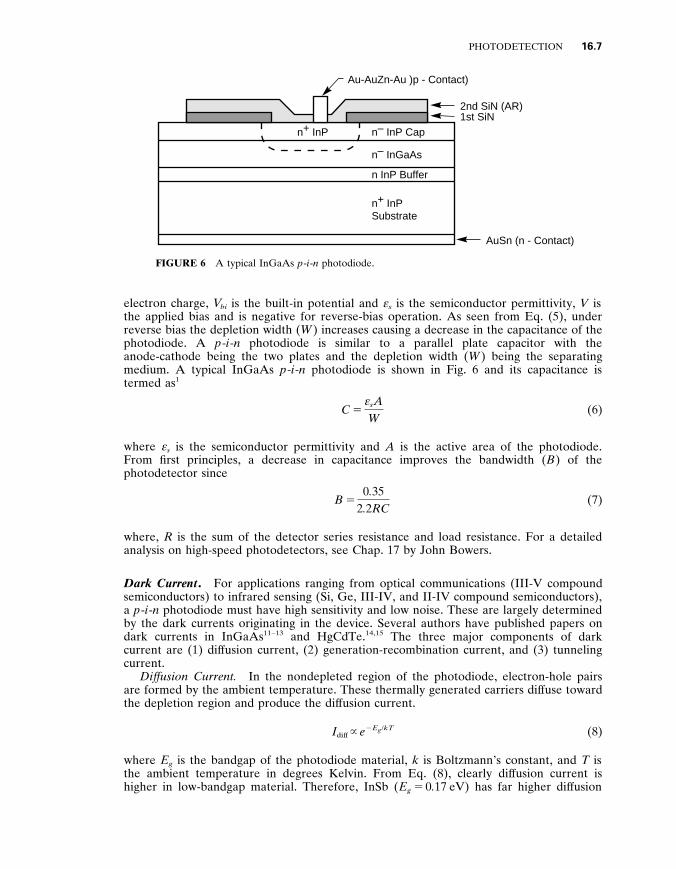
FIGURE 5 A typical photoconductor .
photoconductor is illustrated in Fig . 5 with L being the thickness of the active layer . The transit time ( t r ) requires for a charge carrier to travel a distance L is given by :
t r 5 L 2
m V (3)
where V 5 applied bias and m 5 mobility . The mobility of electrons ( m n ) and that of holes ( m p ) is dif ferent , with ( m n ) being
usually far higher than ( m p ) . This causes a dif ference in the transit time of electrons and holes . Hence , photon-generated electrons are swept away more quickly than holes which result in a positive charge in the active layer . To maintain the charge neutrality , new electrons are supplied by the external voltage source . Therefore , for one incident photon , more than one electron is circulated in the electric circuit . This results in an ‘‘ef fective gain . ’’ Thus , photoconductor gain can be defined as the ratio of slower transit time ( t p ) to faster transit time ( t n ) .
M 5 t p
t n or
m n
m p (4)
The slower the transit time , the higher the gain ; however , the bandwidth of the device is reduced . Hence , high-gain photoconductors will result in slow devices and vice versa . Such ‘‘high-gain , slow devices’’ can be best utilized for imaging applications . 3 For high-speed optical communication applications in the 1000 – 1700-nm spectrum , InGaAs is the material of choice due to its high mobility . Several reports have been published on high-speed InGaAs photoconductors that find practical applications in optical receivers . 4 – 9 (Also see Chap . 17 , ‘‘High-Speed Photodetectors , ’’ by J . Bowers . )
p - i - n Photodiode
Unlike photoconductors , a photodiode has a p - n junction , usually formed by dif fusion or epitaxy . In a photoconductor , metal contacts are made to either n - or p -type material . However , a photodiode consists of both n - and p -type materials across which a natural electric field is generated . This field is known as the built - in potential ( V b i ) and its value depends on the bandgap of its material . A silicon p - n junction has V b i of 0 . 7 V whereas in germanium it is 0 . 3 V . The higher the bandgap ( E g ) , the larger the built-in potential ( V b i ) . An important physical phenomenon called depletion occurs when a p -type semiconductor is merged with an n -type semiconductor . After an initial exchange of charge , a potential is built up to prevent further flow of charge . This built-in field creates the depletion width ( W ) , which is a region free of any charge carriers and is given by 1 0
W 5 – 2 » s ( N A 1 N D ) q ( N A N D )
( V b i 2 V ) (5)
where N A and N D are impurity concentrations of p side and n side , respectively , q is the
PHOTODETECTION 16 .7
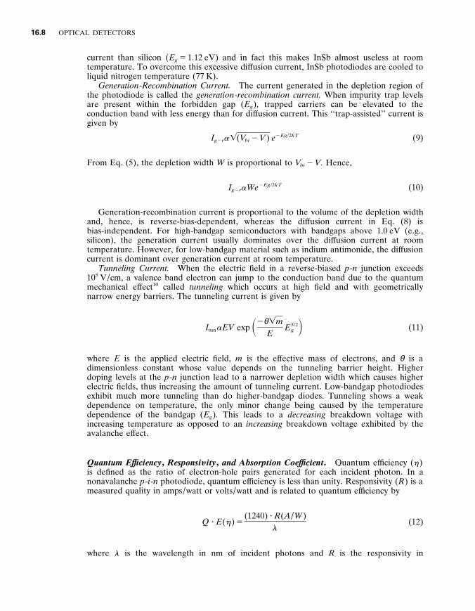
2nd SiN (AR)
Au-AuZn-Au )p - Contact)
1st SiN
AuSn (n - Contact)
n– InP Cap
n– InGaAs
n InP Buffer
n+ InP Substrate
n+ InP
FIGURE 6 A typical InGaAs p - i - n photodiode .
electron charge , V b i is the built-in potential and » s is the semiconductor permittivity , V is the applied bias and is negative for reverse-bias operation . As seen from Eq . (5) , under reverse bias the depletion width ( W ) increases causing a decrease in the capacitance of the photodiode . A p - i - n photodiode is similar to a parallel plate capacitor with the anode-cathode being the two plates and the depletion width ( W ) being the separating medium . A typical InGaAs p - i - n photodiode is shown in Fig . 6 and its capacitance is termed as 1
C 5 » s A
W (6)
where » s is the semiconductor permittivity and A is the active area of the photodiode . From first principles , a decrease in capacitance improves the bandwidth ( B ) of the photodetector since
B 5 0 . 35
2 . 2 RC (7)
where , R is the sum of the detector series resistance and load resistance . For a detailed analysis on high-speed photodetectors , see Chap . 17 by John Bowers .
Dark Current . For applications ranging from optical communications (III-V compound semiconductors) to infrared sensing (Si , Ge , III-IV , and II-IV compound semiconductors) , a p - i - n photodiode must have high sensitivity and low noise . These are largely determined by the dark currents originating in the device . Several authors have published papers on dark currents in InGaAs 1 1 – 1 3 and HgCdTe . 14 , 15 The three major components of dark current are (1) dif fusion current , (2) generation-recombination current , and (3) tunneling current .
Dif fusion Current . In the nondepleted region of the photodiode , electron-hole pairs are formed by the ambient temperature . These thermally generated carriers dif fuse toward the depletion region and produce the dif fusion current .
I dif f ~ e 2 E g / kT (8)
where E g is the bandgap of the photodiode material , k is Boltzmann’s constant , and T is the ambient temperature in degrees Kelvin . From Eq . (8) , clearly dif fusion current is higher in low-bandgap material . Therefore , InSb ( E g 5 0 . 17 eV) has far higher dif fusion
16 .8 OPTICAL DETECTORS
current than silicon ( E g 5 1 . 12 eV) and in fact this makes InSb almost useless at room temperature . To overcome this excessive dif fusion current , InSb photodiodes are cooled to liquid nitrogen temperature (77 K) .
Generation - Recombination Current . The current generated in the depletion region of the photodiode is called the generation - recombination current . When impurity trap levels are present within the forbidden gap ( E g ) , trapped carriers can be elevated to the conduction band with less energy than for dif fusion current . This ‘‘trap-assisted’’ current is given by
I g 2 r a 4 ( V b i 2 V ) e 2 Eg /2 kT (9)
From Eq . (5) , the depletion width W is proportional to V b i 2 V . Hence ,
I g 2 r a We 2 Eg /2 kT (10)
Generation-recombination current is proportional to the volume of the depletion width and , hence , is reverse-bias-dependent , whereas the dif fusion current in Eq . (8) is bias-independent . For high-bandgap semiconductors with bandgaps above 1 . 0 eV (e . g ., silicon) , the generation current usually dominates over the dif fusion current at room temperature . However , for low-bandgap material such as indium antimonide , the dif fusion current is dominant over generation current at room temperature .
Tunneling Current . When the electric field in a reverse-biased p - n junction exceeds 10 5 V / cm , a valence band electron can jump to the conduction band due to the quantum mechanical ef fect 1 0 called tunneling which occurs at high field and with geometrically narrow energy barriers . The tunneling current is given by
I t u n a EV exp S 2 θ 4 m
E E 3/2
g D (11)
where E is the applied electric field , m is the ef fective mass of electrons , and θ is a dimensionless constant whose value depends on the tunneling barrier height . Higher doping levels at the p - n junction lead to a narrower depletion width which causes higher electric fields , thus increasing the amount of tunneling current . Low-bandgap photodiodes exhibit much more tunneling than do higher-bandgap diodes . Tunneling shows a weak dependence on temperature , the only minor change being caused by the temperature dependence of the bandgap ( E g ) . This leads to a decreasing breakdown voltage with increasing temperature as opposed to an increasing breakdown voltage exhibited by the avalanche ef fect .
Quantum Ef ficiency , Responsi y ity , and Absorption Coef ficient . Quantum ef ficiency ( h ) is defined as the ratio of electron-hole pairs generated for each incident photon . In a nonavalanche p - i - n photodiode , quantum ef ficiency is less than unity . Responsivity ( R ) is a measured quality in amps / watt or volts / watt and is related to quantum ef ficiency by
Q ? E ( h ) 5 (1240) ? R ( A / W )
l (12)
where l is the wavelength in nm of incident photons and R is the responsivity in
PHOTODETECTION 16 .9
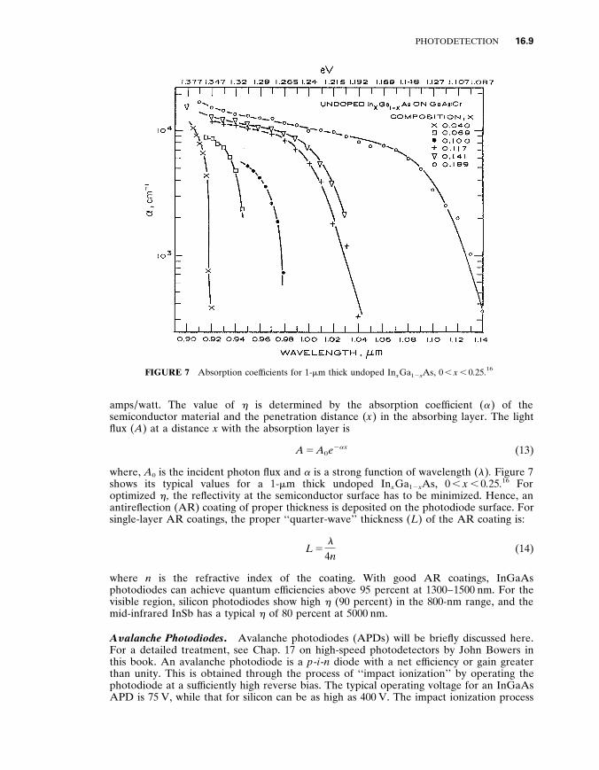
FIGURE 7 Absorption coef ficients for 1- m m thick undoped In x Ga 1 2 x As , 0 , x , 0 . 25 . 1 6
amps / watt . The value of h is determined by the absorption coef ficient ( a ) of the semiconductor material and the penetration distance ( x ) in the absorbing layer . The light flux ( A ) at a distance x with the absorption layer is
A 5 A 0 e 2 a x (13)
where , A 0 is the incident photon flux and a is a strong function of wavelength ( l ) . Figure 7 shows its typical values for a 1- m m thick undoped In x Ga 1 2 x As , 0 , x , 0 . 25 . 1 6 For optimized h , the reflectivity at the semiconductor surface has to be minimized . Hence , an antireflection (AR) coating of proper thickness is deposited on the photodiode surface . For single-layer AR coatings , the proper ‘‘quarter-wave’’ thickness ( L ) of the AR coating is :
L 5 l
4 n (14)
where n is the refractive index of the coating . With good AR coatings , InGaAs photodiodes can achieve quantum ef ficiencies above 95 percent at 1300 – 1500 nm . For the visible region , silicon photodiodes show high h (90 percent) in the 800-nm range , and the mid-infrared InSb has a typical h of 80 percent at 5000 nm .
A y alanche Photodiodes . Avalanche photodiodes (APDs) will be briefly discussed here . For a detailed treatment , see Chap . 17 on high-speed photodetectors by John Bowers in this book . An avalanche photodiode is a p - i - n diode with a net ef ficiency or gain greater than unity . This is obtained through the process of ‘‘impact ionization’’ by operating the photodiode at a suf ficiently high reverse bias . The typical operating voltage for an InGaAs APD is 75 V , while that for silicon can be as high as 400 V . The impact ionization process
16 .10 OPTICAL DETECTORS
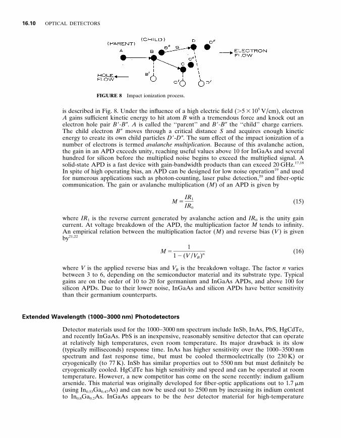
FIGURE 8 Impact ionization process .
is described in Fig . 8 . Under the influence of a high electric field ( . 5 3 10 5 V / cm) , electron A gains suf ficient kinetic energy to hit atom B with a tremendous force and knock out an electron hole pair B 9 - B 0 . A is called the ‘‘parent’’ and B 9 - B 0 the ‘‘child’’ charge carriers . The child electron B 0 moves through a critical distance S and acquires enough kinetic energy to create its own child particles D 9 - D 0 . The sum ef fect of the impact ionization of a number of electrons is termed a y alanche multiplication . Because of this avalanche action , the gain in an APD exceeds unity , reaching useful values above 10 for InGaAs and several hundred for silicon before the multiplied noise begins to exceed the multiplied signal . A solid-state APD is a fast device with gain-bandwidth products than can exceed 20 GHz . 17 , 18
In spite of high operating bias , an APD can be designed for low noise operation 1 9 and used for numerous applications such as photon-counting , laser pulse detection , 2 0 and fiber-optic communication . The gain or avalanche multiplication ( M ) of an APD is given by
M 5 IR 1
IR 0 (15)
where IR 1 is the reverse current generated by avalanche action and IR 0 is the unity gain current . At voltage breakdown of the APD , the multiplication factor M tends to infinity . An empirical relation between the multiplication factor ( M ) and reverse bias ( V ) is given by 21 , 22
M 5 1
1 2 ( V / V B ) n (16)
where V is the applied reverse bias and V B is the breakdown voltage . The factor n varies between 3 to 6 , depending on the semiconductor material and its substrate type . Typical gains are on the order of 10 to 20 for germanium and InGaAs APDs , and above 100 for silicon APDs . Due to their lower noise , InGaAs and silicon APDs have better sensitivity than their germanium counterparts .
Extended Wavelength (1000 – 3000 nm) Photodetectors
Detector materials used for the 1000 – 3000 nm spectrum include InSb , InAs , PbS , HgCdTe , and recently InGaAs . PbS is an inexpensive , reasonably sensitive detector that can operate at relatively high temperatures , even room temperature . Its major drawback is its slow (typically milliseconds) response time . InAs has higher sensitivity over the 1000 – 3500 nm spectrum and fast response time , but must be cooled thermoelectrically (to 230 K) or cryogenically (to 77 K) . InSb has similar properties out to 5500 nm but must definitely be cryogenically cooled . HgCdTe has high sensitivity and speed and can be operated at room temperature . However , a new competitor has come on the scene recently : indium gallium arsenide . This material was originally developed for fiber-optic applications out to 1 . 7 m m (using In 0 . 53 Ga 0 . 47 As) and can now be used out to 2500 nm by increasing its indium content to In 0 . 8 Ga 0 . 2 As . InGaAs appears to be the best detector material for high-temperature
PHOTODETECTION 16 .11
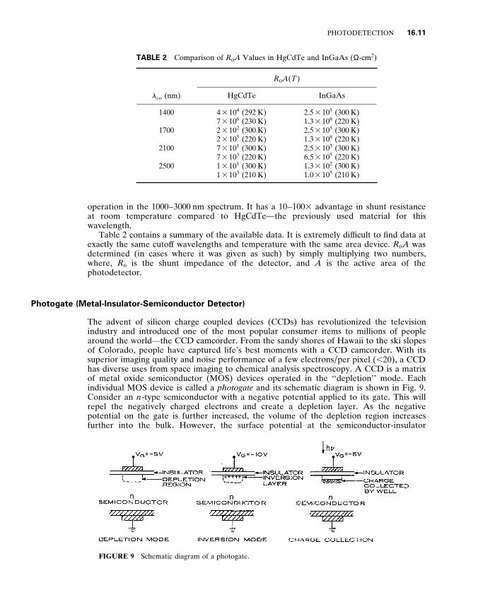
TABLE 2 Comparison of R 0 A Values in HgCdTe and InGaAs ( Ω -cm 2 )
R 0 A ( T )
l c o (nm) HgCdTe InGaAs
1400
1700
2100
2500
4 3 10 4 (292 K) 7 3 10 6 (230 K) 2 3 10 2 (300 K) 2 3 10 5 (220 K) 7 3 10 1 (300 K) 7 3 10 3 (220 K) 1 3 10 1 (300 K) 1 3 10 3 (210 K)
2 . 5 3 10 5 (300 K) 1 . 3 3 10 8 (220 K) 2 . 5 3 10 5 (300 K) 1 . 3 3 10 8 (220 K) 2 . 5 3 10 3 (300 K) 6 . 5 3 10 5 (220 K) 1 . 3 3 10 2 (300 K) 1 . 0 3 10 5 (210 K)
operation in the 1000 – 3000 nm spectrum . It has a 10 – 100 3 advantage in shunt resistance at room temperature compared to HgCdTe—the previously used material for this wavelength .
Table 2 contains a summary of the available data . It is extremely dif ficult to find data at exactly the same cutof f wavelengths and temperature with the same area device . R 0 A was determined (in cases where it was given as such) by simply multiplying two numbers , where , R 0 is the shunt impedance of the detector , and A is the active area of the photodetector .
Photogate (Metal-Insulator-Semiconductor Detector)
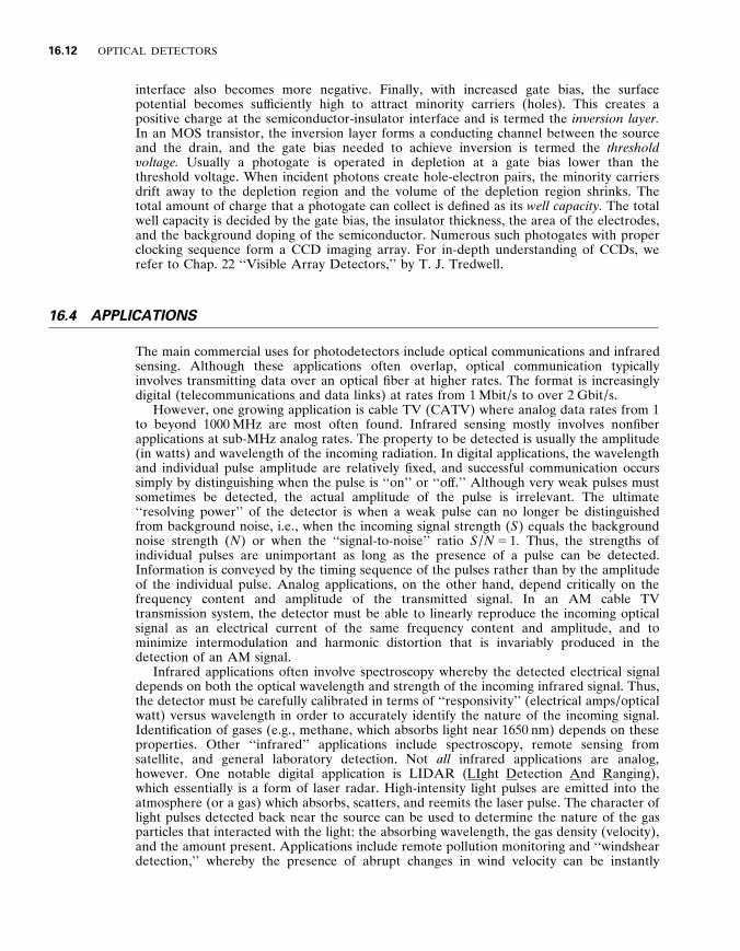
The advent of silicon charge coupled devices (CCDs) has revolutionized the television industry and introduced one of the most popular consumer items to millions of people around the world—the CCD camcorder . From the sandy shores of Hawaii to the ski slopes of Colorado , people have captured life’s best moments with a CCD camcorder . With its superior imaging quality and noise performance of a few electrons / per pixel ( , 20) , a CCD has diverse uses from space imaging to chemical analysis spectroscopy . A CCD is a matrix of metal oxide semiconductor (MOS) devices operated in the ‘‘depletion’’ mode . Each individual MOS device is called a photogate and its schematic diagram is shown in Fig . 9 . Consider an n -type semiconductor with a negative potential applied to its gate . This will repel the negatively charged electrons and create a depletion layer . As the negative potential on the gate is further increased , the volume of the depletion region increases further into the bulk . However , the surface potential at the semiconductor-insulator
FIGURE 9 Schematic diagram of a photogate .
16 .12 OPTICAL DETECTORS
interface also becomes more negative . Finally , with increased gate bias , the surface potential becomes suf ficiently high to attract minority carriers (holes) . This creates a positive charge at the semiconductor-insulator interface and is termed the in y ersion layer . In an MOS transistor , the inversion layer forms a conducting channel between the source and the drain , and the gate bias needed to achieve inversion is termed the threshold y oltage . Usually a photogate is operated in depletion at a gate bias lower than the threshold voltage . When incident photons create hole-electron pairs , the minority carriers drift away to the depletion region and the volume of the depletion region shrinks . The total amount of charge that a photogate can collect is defined as its well capacity . The total well capacity is decided by the gate bias , the insulator thickness , the area of the electrodes , and the background doping of the semiconductor . Numerous such photogates with proper clocking sequence form a CCD imaging array . For in-depth understanding of CCDs , we refer to Chap . 22 ‘‘Visible Array Detectors , ’’ by T . J . Tredwell .
1 6 . 4 APPLICATIONS
The main commercial uses for photodetectors include optical communications and infrared sensing . Although these applications often overlap , optical communication typically involves transmitting data over an optical fiber at higher rates . The format is increasingly digital (telecommunications and data links) at rates from 1 Mbit / s to over 2 Gbit / s .
However , one growing application is cable TV (CATV) where analog data rates from 1 to beyond 1000 MHz are most often found . Infrared sensing mostly involves nonfiber applications at sub-MHz analog rates . The property to be detected is usually the amplitude (in watts) and wavelength of the incoming radiation . In digital applications , the wavelength and individual pulse amplitude are relatively fixed , and successful communication occurs simply by distinguishing when the pulse is ‘‘on’’ or ‘‘of f . ’’ Although very weak pulses must sometimes be detected , the actual amplitude of the pulse is irrelevant . The ultimate ‘‘resolving power’’ of the detector is when a weak pulse can no longer be distinguished from background noise , i . e ., when the incoming signal strength ( S ) equals the background noise strength ( N ) or when the ‘‘signal-to-noise’’ ratio S / N 5 1 . Thus , the strengths of individual pulses are unimportant as long as the presence of a pulse can be detected . Information is conveyed by the timing sequence of the pulses rather than by the amplitude of the individual pulse . Analog applications , on the other hand , depend critically on the frequency content and amplitude of the transmitted signal . In an AM cable TV transmission system , the detector must be able to linearly reproduce the incoming optical signal as an electrical current of the same frequency content and amplitude , and to minimize intermodulation and harmonic distortion that is invariably produced in the detection of an AM signal .
Infrared applications often involve spectroscopy whereby the detected electrical signal depends on both the optical wavelength and strength of the incoming infrared signal . Thus , the detector must be carefully calibrated in terms of ‘‘responsivity’’ (electrical amps / optical watt) versus wavelength in order to accurately identify the nature of the incoming signal . Identification of gases (e . g ., methane , which absorbs light near 1650 nm) depends on these properties . Other ‘‘infrared’’ applications include spectroscopy , remote sensing from satellite , and general laboratory detection . Not all infrared applications are analog , however . One notable digital application is LIDAR ( LIght Detection And Ranging) , which essentially is a form of laser radar . High-intensity light pulses are emitted into the atmosphere (or a gas) which absorbs , scatters , and reemits the laser pulse . The character of light pulses detected back near the source can be used to determine the nature of the gas particles that interacted with the light : the absorbing wavelength , the gas density (velocity) , and the amount present . Applications include remote pollution monitoring and ‘‘windshear detection , ’’ whereby the presence of abrupt changes in wind velocity can be instantly
PHOTODETECTION 16 .13
detected at distances of several miles . This application 4 2 has been demonstrated with laser wavelengths of 2060 and 10 , 600 nm for use on aircraft and may be required on all commercial aircraft by the year 1995 . The 2060-nm system works better in severe storms and does not require a cryogenically cooled detector (as does the 10 , 600-nm system) . However , the CO 2 gas laser used for 10 , 600 nm , although bulky and costly , is more highly developed and more readily available than the more recent HO : YAG solid-state lasers used for 2060 nm . 4 2 Further developments will undoubtedly occur here over the next several years .
One important noise source in infrared applications is the so-called 1 / f noise which becomes noticeable at frequencies below 10 MHz . Although poorly understood , this noise is thought to originate at heterointerfaces such as semiconductor-metal contacts and heteroepitaxial interfaces . Photodiode arrays are often required to detect low-light-level signals of a few hundred photons , and they must integrate the signal for 1 second or more . However , with longer integration times , 1 / f noise may become noticeable and can degrade the S / N ratio and thus , impose an upper limit on the ef fectiveness of longer integration times . Limiting 1 / f noise becomes critical for numerous infrared sensing applications and research indicates that surface depletion width at the semiconductor-insulator interface to be a major source of 1 / f noise in the InGaAs photodiodes . 4 4
One important area for detectors is the array configuration used both for spectroscopy (linear) and imaging (two-dimensional) . Linear arrays are used in so-called multichannel analyzers whereby the detector is placed behind a fixed grating and the instrument functions as ‘‘motionless’’ or ‘‘instant’’ spectrometer with each pixel corresponding to a narrow band of wavelengths . The resolution of the instrument is determined by the number and spacing of pixels , so narrow pixel geometries are demanded along one direction whereas tall pixel geometries are demanded along the perpendicular direction to enhance the light collection .
One ‘‘mixed’’ infrared / fiber-optic application is the use of large-area (typically 3-mm diameter) detectors for optical power meters : the optical equivalent of a voltmeter which accurately measures the amount of optical power in watts or dBm (number of decibels above or below 1 mW contained in an incoming beam) . The large area ensures large collection ef ficiency . The most important parameter here is the responsivity and the uniformity of response across the detector .
A ‘‘figure-of-merit’’ for infrared detectors is D * (deestar) , whereby detectors of dif fering area can be compared . It is related to the noise equivalent power (NEP) in watts , the lowest power a detector can detect at a signal-to-noise ratio of 1 as
D *( l , f , B ) 5 ( AB ) 1 / 2 / NEP (17)
where A is the detector area . The optical bandwidth B (often taken to be 1 Hz) , frequency of signal modulation ( f ) , and operating wavelength ( l ) must be stated .
1 6 . 5 RELIABILITY
In today’s global economy of severe competitiveness , new product development and innovation is incomplete without quality assurance and reliability . Reliability is the assurance that a device will perform its stated functions for a certain period of time under stated conditions , and considerable research has been done to improve the reliability of photodetectors . 23–26 The two major industrial standards for testing semiconductor device reliability are : (1) test methods and procedures for microelectronics (MIL . STD . 883C) , and (2) Bellcore technical advisory (TA-TSY-00468) . The former standard is generic to the semiconductor industry , while the latter is specifically developed for fiber-optic opto- electronic devices .
The tests performed under MIL . STD . 883C comprise of the following major groups :
16 .14 OPTICAL DETECTORS
TABLE 3 Electrical and Optical Testing of Photodetectors
Tests or measurement Parameter Symbol References
Optical response Responsivity
Gain
R
G
Bellcore Technology Advisory
Electrical performance
Dark current Breakdown voltage
I d V b r
TA-TSY-00468 Issue 2 , July 1988
(1) en y ironmental tests , e . g ., moisture resistance , burn-in , seal , dew point , thermal shock , (2) mechanical tests , e . g ., constant acceleration , mechanical shock , vibration , solderability , and bond strength , and (3) electrical tests , e . g ., breakdown voltage , transition time measurements , input currents , terminal capacitance , and electrostatic discharge (ESD) sensitivity classification . Under the Bellcore Technical Advisory , each photodetector lot undergoes visual inspection , optical and electrical characterization , and screening . Visual inspection removes any photodiodes with faulty wire bonds or cracks in the glass window or in the insulating films . Table 3 lists the electrical and optical testing performed on every photodiode . After testing , all the devices are sent for screening (burn-in) , e . g ., some In 0 . 53 Ga 0 . 47 As photodiodes are burned-in at 200 8 C for 20 hours at 2 20 V reverse bias to weed out any infant mortality .
Photodetector Life Test (Accelerated Aging)
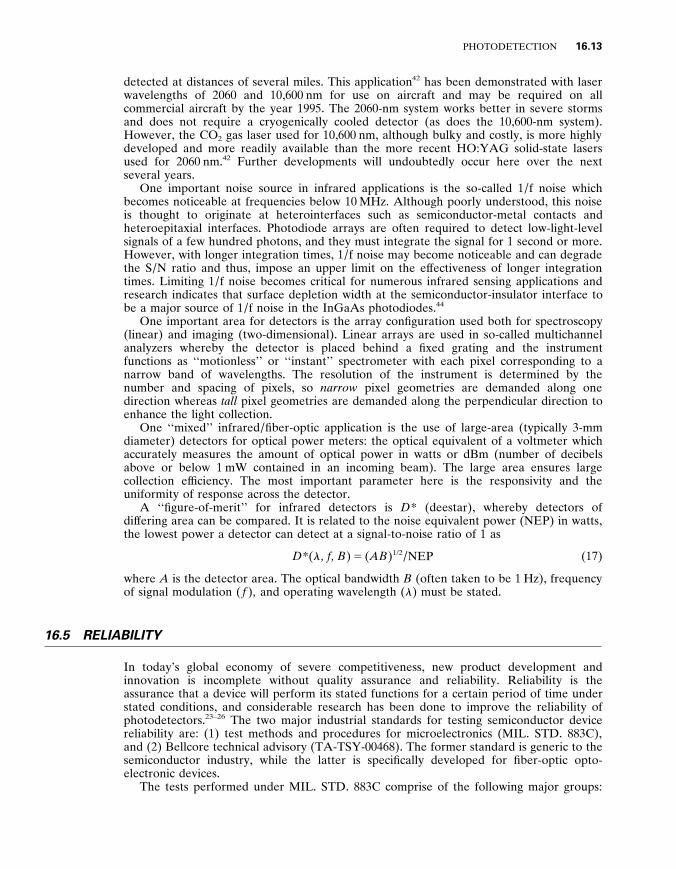
To predict the lifetime or mean - time - to - failure (MTTF) , accelerated aging tests are carried out on groups of diodes at several elevated temperatures . For example , the MTTF for 300- m m diameter InGaAs photodiodes was determined on groups of 20 screened devices at elevated temperatures of 200 , 230 , and 250 8 C . The failure criterion was a 25 percent increase in the room temperature dark current value . 26 , 27 The total lifetest extended over a time period of several years , and every week the samples were cooled to room temperature to check their dark current . Failed devices were removed from the sample population and the remaining good ones put back at the elevated temperature .
From the temperature-dependence of the data , it was observed that the failure mechanism is thermally activated . The Arrhenius relationship calculates the activation energy ( E a ) for thermally activated failure 2 7 as
MTTF(T) 5 Ce ( E a / kT ) (18)
where , C is a constant , k is Boltzmann’s constant (8 . 63 3 10 5 eV / K) , and T is the temperature in Kelvin . Figure 10 shows the MTTF for three batches of 300- m m diameter In 0 . 53 Ga 0 . 47 As / InP photodiodes . Using least-squares fit to the data , the calculated activation energy ( E a ) is 1 . 31 eV with a correlation coef ficient ( r 2 ) of 0 . 99 . From Eq . (18) and an experimentally determined activation energy of 1 . 31 eV , the MTTF at 25 8 C is calculated to be 1 . 34 3 10 1 4 hours . Such a ‘‘geological’’ lifetime may seem to be an overkill , even for the electronics industry . However , when thousands of these devices are working together in a single system (e . g ., telephones) , the net MTTF of all these devices chained together may be on the order of only a few years . Thus , continuing improvements in reliability must be an ongoing process . Reliability in most photodetectors is determined by a number of factors including : (1) material quality , (2) processing procedures , (3) planar technology versus mesa technology , and (4) amount of leakage current . Poor material quality can
PHOTODETECTION 16 .15
FIGURE 10 Time versus cumulative percent failure of InGaAs diodes at 200 , 230 , and 250 8 C lifetest .
introduce crystal defects such as vacancies and dislocations which can increase the dark current . Higher dark current has been directly linked to lower MTTF . 2 6 Device processing is probably the most crucial item in photodetector reliability . The dielectric (typically silicon nitride) used in planar detector processing serves as a dif fusion mask in p - n -junction formation and a passivant (termination) for the junction so produced . Any surface states or impurities introduced here can directly increase leakage current and degrade reliability .
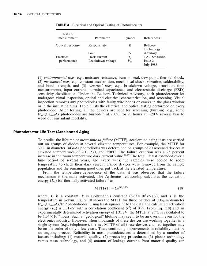
An important milestone in detector reliability was the changeover mesa to planar structures . 2 , 28 Just as the transistors in the 1950s were first made in mesa form , so were the optical photodetectors of the 1980s , due to their simplicity and ease of fabrication . However , in both cases , reliability issues forced the introduction of the more complex planar structure . A sketch of a mesa and planar photodiode is illustrated in Fig . 11 . A mesa photodiode typically is formed by wet chemical etching of an epitaxially grown p - n
FIGURE 11 Sketch of a mesa and planar photodetector .
16 .16 OPTICAL DETECTORS
crystal structure , while in a planar process , a p - n junction is formed by dif fusing a suitable p or n dopant in an n - or p -type crystal . Research shows a planar structure to be more reliable than a mesa one 2 8 because a p - n junction is never exposed to ambient conditions in a well-designed planar process . Exposure of the p - n junction can cause surface corrosion leading to increased leakage current and , in ef fect , poorer reliability . 2 9
1 6 . 6 FUTURE PHOTODETECTORS
In the near future , a lateral p - i - n photodiode and a quantum well infrared photodetector (QWIP) may find increased commercial applications . Both these structures have already been developed in the research laboratories and show promising characteristics compared to the current photodetector structures that they may well replace . A long wavelength QWIP in the 8000 – 12000-nm band 30–33 has posed a severe challenge to the present favorite mercury cadmium telluride photodetectors , while a medium wavelength QWIP in the 3000 – 5000-nm band 3 4 may compete with indium antimonide and platinum silicide photodetectors . A QWIP made from GaAs / AlGaAs heterosystems promises to have higher detectivity ( D *) , higher yield due to well established 3-in wafer GaAs technology , and easier monolithic integration with circuit electronics . A lateral p - i - n diode , as the name implies , has charge carrier flow in a lateral direction compared to the vertical direction in a conventional (vertical) photodiode structure . Because of its process compatibility and simple fabrication , a lateral p - i - n photodiode can be suitably integrated on an optoelectronic integrated circuit (OEIC) chip 35 , 36 having numerous field-ef fect transistors . An OEIC has a lower noise floor due to the reduced stray capacitances and inductances compared to that of hybrid detector-amplifier packages and finds applications in high-speed digital data communication .
Lateral p - i - n Photodetector
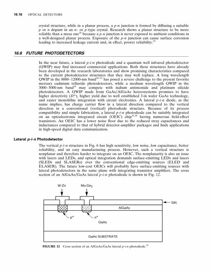
The vertical p - i - n structure in Fig . 6 has high sensitivity , low noise , low capacitance , better reliability , and an easy manufacturing process . However , such a vertical structure is nonplanar and therefore harder to integrate on an OEIC . The nonplanarity is also an issue with lasers and LEDs , and optical integration demands surface-emitting LEDs and lasers (SLEDs and SLASERs) over the conventional edge-emitting sources (ELED and ELASER) . The future low-cost OEICs will probably have surface-emitting sources with lateral photodetectors in the same plane with integrating transistor amplifiers . The cross section of an AlGaAs / GaAs lateral p - i - n photodiode is shown in Fig . 12 .
GaAs SUBSTRATE
GaAs
AlGaAs
Mo-Ge2W-Zn
SiN
p+ n+
FIGURE 12 Cross section of an AlGaAs / GaAs lateral p - i - n photodiode . 3 6
PHOTODETECTION 16 .17
The higher-bandgap AlGaAs layer acts as a surface barrier , reducing the leakage currents . The low-bandgap GaAs layer absorbs the incoming light , and the generated carriers flow to the W-Zn and Mo-Ge 2 ohmic contacts which act as the p region and n region , respectively . The dif fusion of zinc and germanium in the ohmic contacts forms a compositionally graded barrier at the AlGaAs / GaAs interface , rather than an abrupt interface . This smooth barrier helps the lateral p - i - n photodiode to have better speed than a lateral metal-semiconductor-metal photodetector . A comfortable spacing of 3 to 5 m m between the p and n regions gives high quantum ef ficiency and low capacitance , thus providing all the desirable properties of a vertical p - i - n structure and yet being easier to integrate .
Quantum Well Infrared Photodetector (QWIP)
QWIPs of fer the possibility of achieving long wavelength (5000 – 10 , 000 nm) infrared detection by using materials whose bandgap normally allows them only to absorb light in the short wavelength ( , 10 , 000 nm) region , e . g ., GaAs / AlGaAs . The use of thin ( , 500 Å ) layers allows the absorbing wavelength to be controlled by material geometry rather than material chemistry . 3 7
Before discussing the QWIPs , we take the liberty of explaining a few basic terms and concepts of quantum physics . Superlattices or quantum well structures consist of a stack of ultrathin semiconductor layers normally 50 to 500 Å in thickness . Molecular beam epitaxy (MBE) techniques are frequently employed to grow these structures because their characteristically slow growth rate of a few Angstroms / sec which helps achieve abrupt heterointerfaces . Two semiconductors of dif ferent compositions , when stacked together , form a heterointerface . Type III-V compound semiconductors such as AlGaAs / GaAs and InAlAs / InGaAs are the best candidates for growing quantum well structures , as they can be easily doped and their alloy composition readily changed to form semiconductor layers of dif ferent bandgaps . Tailoring the bandgap can alter the heterobarriers , creating exciting device results . When quantum well layers have thicknesses less than the electron mean free path (typically 50 to 100 Å ) , electron and holes cannot have their normal three- dimensional motion . This restricts carriers to move in two dimensions in the plane of the layer . 2 , 37 Because of this quantized motion , a new band of discrete energy levels is generated . Carriers no longer obey Boltzmann’s statistics 1 and optical absorption becomes more complicated than the conventional band-to-band absorption given by Eq . (1) . The absorption of light energy by a quantum well structure can cause an electron to jump from ‘‘multiple valence subbands’’ to ‘‘multiple conduction subbands , ’’ thereby enabling it to absorb light wavelengths not decided by the material properties (bandgap) of the semiconductor layers alone , but by its geometrical properties as well .
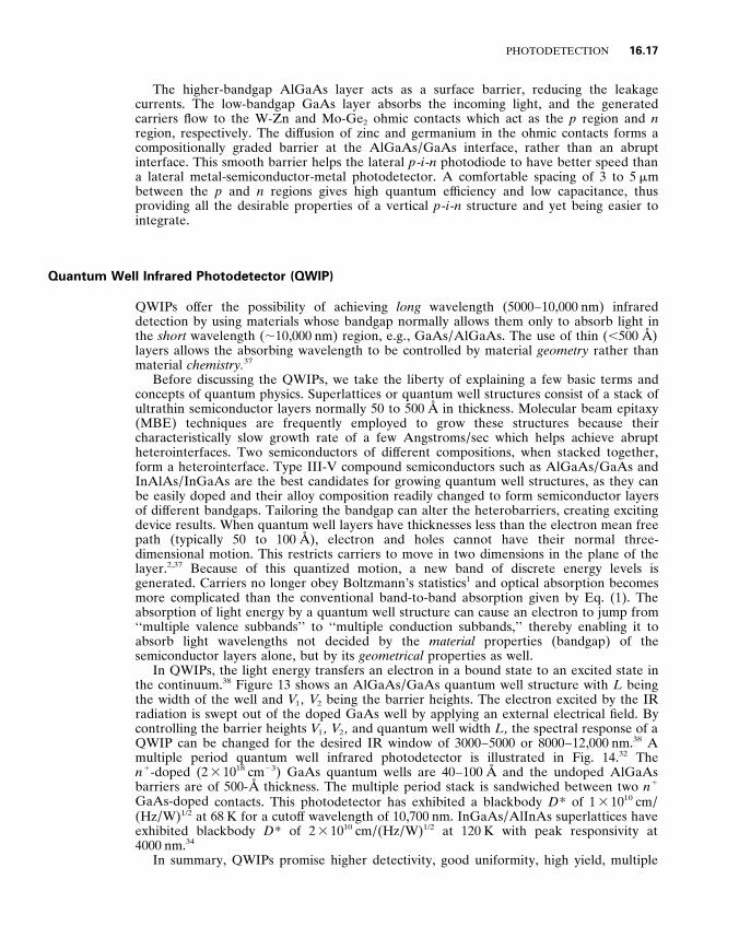
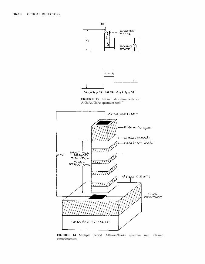
In QWIPs , the light energy transfers an electron in a bound state to an excited state in the continuum . 3 8 Figure 13 shows an AlGaAs / GaAs quantum well structure with L being the width of the well and V 1 , V 2 being the barrier heights . The electron excited by the IR radiation is swept out of the doped GaAs well by applying an external electrical field . By controlling the barrier heights V 1 , V 2 , and quantum well width L , the spectral response of a QWIP can be changed for the desired IR window of 3000 – 5000 or 8000 – 12 , 000 nm . 3 8 A multiple period quantum well infrared photodetector is illustrated in Fig . 14 . 3 2 The n 1 -doped (2 3 10 1 8 cm 2 3 ) GaAs quantum wells are 40 – 100 Å and the undoped AlGaAs barriers are of 500- Å thickness . The multiple period stack is sandwiched between two n 1
GaAs-doped contacts . This photodetector has exhibited a blackbody D * of 1 3 10 1 0 cm / (Hz / W) 1 / 2 at 68 K for a cutof f wavelength of 10 , 700 nm . InGaAs / AlInAs superlattices have exhibited blackbody D * of 2 3 10 1 0 cm / (Hz / W) 1 / 2 at 120 K with peak responsivity at 4000 nm . 3 4
In summary , QWIPs promise higher detectivity , good uniformity , high yield , multiple
16 .18 OPTICAL DETECTORS
FIGURE 13 Infrared detection with an AlGaAs / GaAs quantum well . 3 8
FIGURE 14 Multiple period AlGaAs / GaAs quantum well infrared photodetectors .
PHOTODETECTION 16 .19
spectral windows , and intrinsic radiation hardness , thereby making them attractive for numerous imaging and spectroscopy applications . 3 9
1 6 . 7 ACKNOWLEDGMENT
We sincerely acknowledge the support of EPITAXX , Inc ., Amy Vasger , and Jennifer Romano (Sensors Unlimited) for preparing the manuscript , and Jim Rue for his technical discussions .
1 6 . 8 REFERENCES
1 . S . M . Sze , Physics of Semiconductor De y ices , Wiley , 1981 . 2 . S . R . Forrest , ‘‘Optical Detectors for Lightwave Communication , ’’ Optical Fiber Telecommunica-
tions II , 1988 , pp . 569 – 599 . 3 . Z . S . Huang and T . Ando , ‘‘A Novel Amplified Image Sensor with a Si : H Photoconductor and
MOS Transistors , ’’ IEEE Trans . on Elect . De y . , vol . 37 , no . 6 , 1990 , pp . 1432 – 1438 . 4 . J . C . Gammel , G . M . Metze , and J . M . Ballantyne , ‘‘A Photoconductor Detector for High Speed
Fiber Communication , ’’ IEEE Trans . on Elect . De y . , vol . ED-28 , no . 7 , 1981 , pp . 841 – 849 . 5 . M . V . Rao , P . K . Bhattacharya , and C . Y . Chen , ‘‘Low Noise In 0 . 53 Ga 0 . 47 As : Fe Photoconductive
Detectors for Optical Communications , ’’ IEEE Trans . on Elect . De y . , vol . Ed-33 , no . 1 , 1986 , pp . 67 – 71 .
6 . J . C . Gammel , H . Ohno , and J . M . Ballantyne , ‘‘High Speed Photoconductive Detectors Using GaInAs , ’’ IEEE J . of Quantum Elect . , vol . QE-17 , no . 2 , 1981 , pp . 269 – 272 .
7 . C . Y . Chen , Y . M . Pang , K . Alavi , A . Y . Cho , and P . A . Garbinski , ‘‘Interdigitated Al 0 . 48 In 0 . 52 AsGa 0 . 47 In 0 . 53 As Photoconductive Detectors , ’’ App . Phys . Lett . 44 , 1983 , pp . 99 – 101 .
8 . M . V . Rao , G . K . Chang , and W . P . Hong , ‘‘High Sensitivity , High Speed InGaAs Photoconduc- tive Detector , ’’ Elect . Lett . , vol . 26 , no . 11 , 1990 , pp . 756 – 757 .
9 . J . Degani , R . F . Leheny , R . E . Nahory , M . A . Pollack , J . P . Heritage , and J . C . DeWinter , ‘‘Fast Photoconductive Detector Using p-In 0 . 53 Ga 0 . 47 As with Response to 1 . 7 m m , ’’ Appl . Phys . Lett . 38 , 1981 , pp . 27 – 29 .
10 . S . M . Sze , Semiconductor De y ices — Physics and Technology , Wiley , 1985 . 11 . G . H . Olsen , ‘‘Low Leakage , High Ef ficiency , Reliable VPE InGaAs 1 . 0-1 . 7 m m Photodiodes , ’’
IEEE Elect . De y . Lett . , vol . EDL-2 , no . 9 , 1981 , pp . 217 – 219 . 12 . S . R . Forrest , ‘‘Performance of In x Ga 1 2 x As y P 1 2 y Photodiodes with Dark Current Limited by
Dif fusion , Generation Recombination and Tunneling , ’’ IEEE J . of Quantum Elect . , vol . QE-17 , no . 2 , 1981 , pp . 217 – 226 .
13 . O . K . Kim , B . V . Dutt , R . J . McCoy , and J . R . Zuber , ‘‘A Low Dark-Current , Planar InGaAs p - i - n Photodiode with a Quaternary InGaAsP Cap Layer , ’’ IEEE J . of Quantum Elect . , vol . QE-21 , no . 2 , 1985 , pp . 138 – 143 .
14 . Y . Yoshida , Y . Hisa , T . Takiguchi , and Y . Komine , ‘‘Reduction of Surface Leakage Current in Cd 0 . 2 Hg 0 . 8 Te Photodiode , ’’ Proc . SPIE , vol . 972 , 1988 , pp . 39 – 43 .
15 . J . C . Flachet , M . Royer , Y . Carpentier , and G . Pichard , ‘‘Emission and Detection in the 1 to 3 m m Spectral Range with Hg 1 2 x Cd x Te Diodes , ’’ Proc . SPIE , vol . 587 , 1985 , pp . 149 – 155 .
16 . R . E . Enstrom , P . J . Zanucchi , and J . R . Appert , ‘‘Optical Properties of Vapor-Grown In x Ga 1 2 x As Epitaxial Films on GaAs and In x Ga 1 2 x P Substrates , ’’ J . of Appl . Phys . , vol . 45 , no . 1 , 1974 , pp . 300 – 306 .
17 . H . W . Ruegg , ‘‘An Optimized Avalanche Photodiode , ’’ IEEE Trans . on Elect . De y . , vol . Ed-14 , no . 5 , 1967 , pp . 239 – 251 .
16 .20 OPTICAL DETECTORS
18 . K . Taguchi , T . Torikai , Y . Sugimoto , K . Makita , and H . Ishihara , ‘‘Planar Structure InP / InGaAsP / InGaAs Avalanche Photodiodes with Preferential Lateral Extended Guard Ring for 1 . 0 – 1 . 6 m m Wavelength Optical Communication Use , ’’ J . of Lightwa y e Tech . , vol . 6 , no . 11 , pp . 1643 – 1655 .
19 . S . R . Forrest , R . G . Smith , and O . K . Kim , ‘‘Performance of In 0 . 53 Ga 0 . 47 As / InP Avalanche Photodiodes , ’’ IEEE J . of Quantum Elect . , vol . QE-18 , no . 12 , 1982 , pp . 2040 – 2047 .
20 . R . J . McIntyre , ‘‘The Distribution of Gains in Uniformly Multiplying Avalanche Photodiodes : Theory , ’’ IEEE Trans . on Elect . De y . , vol . ED-19 , no . 6 , 1972 , pp . 703 – 713 .
21 . A . S . Grove , Physics and Technology of Semiconductor De y ices , Wiley , 1967 . 22 . S . L . Miller , ‘‘Avalanche Breakdown in Germanium , ’’ Phys . Re y . , vol . 99 , 1955 , p . 1234 . 23 . R . U . Martinelli and R . E . Enstrom , ‘‘Reliability of Planar InGaAs / InP Photodiodes Passivated
with BoroPhosho-Silicate Glass , ’’ J . of Appl . Phys . , vol . 63 , no . 1 , 1988 , pp . 250 – 252 . 24 . A . K . Chin , F . S . Chen , and F . Ermanis , ‘‘Failure Mode Analysis of Planar Zinc-Dif fused
In 0 . 53 Ga 0 . 47 As p - i - n Photodiodes , ’’ J . of Appl . Phys . , vol . 55 , no . 6 , 1984 , pp . 1596 – 1606 . 25 . Y . Kuhara , H . Tercuchi , and H . Nishizawa , ‘‘Reliability of InGaAs / InP Long Wavelength p - i - n
Photodiodes Passivated with Polymide Thin Film , ’’ IEEE J . of Lightwa y e Tech . , vol . LT-4 , no . 7 , 1986 , pp . 933 – 937 .
26 . A . M . Joshi , G . H . Olsen , and S . R . Patil , ‘‘Reliability of InGaAs Detectors and Arrays , ’’ Proc . SPIE , vol . 1580 , 1991 , pp . 34 – 40 .
27 . S . R . Forrest , V . S . Ban , G . Gasparian , D . Gay , and G . H . Olsen , ‘‘Reliability of Vapor Grown In 0 . 53 Ga 0 . 47 As / InP p - i - n Photodiodes With Very High Failure Activation Energy , ’’ IEEE Elect . De y . Lett . , vol . 9 , no . 5 , 1988 , pp . 217 – 219 .
28 . C . P . Skrimshire , J . R . Farr , D . F . Sloan , M . J . Robertson , P . A . Putland , J . C . D . Stokoe , and R . R . Sutherland , ‘‘Reliability of Mesa and Planar InGaAs p - i - n Photodiodes , ’’ IEEE Proc . , vol . 137 , part J , no . 1 , 1990 , p . 7478 .
29 . R . R . Sutherland , J . C . D . Stokoe , C . P . Skrimshire , B . M . Macdonald , and D . F . Sloan , ‘‘The Reliability of Planar InGaAs / InP p - i - n Photodiodes with Organic Coatings for Use in Low Cost Receiver , ’’ Proc . SPIE , vol . 1174 , 1989 , pp . 226 – 232 .
30 . B . F . Levine , C . G . Bethea , G . Hasnain , V . O . Shen , E . Pelve , R . R . Abbott , and S . J . Hsieh , ‘‘High Sensitivity Low Dark Current 10 m m GaAs Quantum Well Infrared Photodetectors , ’’ Appl . Physics Lett . , vol . 56(9) , 1990 , pp . 851 – 853 .
31 . B . F . Levine , C . G . Bethea , V . O . Shen , and R . J . Malik , ‘‘Tunable Long-Wavelength Detectors Using Graded Quantum Wells Grown by Electron Beam Source Molecular Beam Epitaxy , ’’ Appl . Phys . Lett . , vol . 57(4) , 1990 , pp . 383 – 385 .
32 . G . Hasnain , B . F . Levine , S . Gunapala , and N . Chand , ‘‘Large Photoconductive Gain In Quantum Well Infrared Photodetectors , ’’ Appl . Phys . Lett . , vol . 57(6) , 1990 , pp . 608 – 610 .
33 . E . Pelve , F . Beltram , C . G . Bethea , B . F . Levine , V . O . Shen , S . J . Hsieh , and R . R . Abbott , ‘‘Analysis of the Dark Current in Doped Well Multiple Quantum Well AlGaAs Infrared Photodetectors , ’’ J . of Appl . Phys . , vol . 66(11) , 1989 , pp . 5656 – 5658 .
34 . G . Hasnain , B . F . Levine , D . L . Sivco , and A . Y . Cho , ‘‘Mid-Infrared Detectors in the 3 – 5 m m Band Using Bound to Continuum State Absorption in InGaAs / InAlAs Multiquantum Well Structures , ’’ Appl . Phys . Lett . , vol . 56(8) , 1990 , pp . 770 – 772 .
35 . S . N . Subbarao , D . W . Bechtle , R . J . Menna , J . C . Connolly , R . L . Camisa , and S . Y . Narayan , ‘‘2 – 4 GHz Monolithic Lateral p - i - n Photodetector and MESFET Amplifier on GaAs-onSi , ’’ IEEE Trans . on Microwa y e Theory and Tech . , vol . 38 , no . 9 , 1990 , pp . 1199 – 1202 .
36 . S . Tiwari , J . Burroughs , M . S . Milshtein , M . A . Tischler , and S . L . Wright , ‘‘Lateral p - i - n Photodetectors with 18 GHz Bandwidth at 1 . 3 m m Wavelength and Small Bias Voltages , ’’ Tech . Dig . of IEEE Int . Elect . De y . Mtg . , 1991 , pp . 421 – 425 .
37 . D . S . Chemla , ‘‘Quantum Wells for Photonics , ’’ Physics Today , May 1995 , pp . 56 – 64 . 38 . D . D . Coon and R . P . G . Karunasiri , ‘‘New Mode of IR Detection Using Quantum Wells , ’’ App .
Phys . Lett . , vol . 45(6) , 1984 , pp . 649 – 651 . 39 . B . F . Levine , C . G . Bethea , J . W . Stayt , K . G . Glogovski , R . E . Leibenguth , S . D . Gunapala ,
PHOTODETECTION 16 .21
S . S . Pei , and J . M . Kuo , ‘‘Long Wavelength GaAs / Al x Ga 1 2 x As Quantum Well Infrared Photodetectors (QWIPs) , ’’ Proc . SPIE , vol . 1540 , 1991 , pp . 232 – 238 .
40 . G . H . Olsen , ‘‘Reliable Operation of Lattice Mismatched InGaAs Detectors on Silicon , ’’ Tech . Dig . of IEEE Int . Elect . De y . Mtg . , 1990 , pp . 145 – 147 .
41 . E . L . Dereniak and D . G . Crowe , Optical Radiation Detectors , Wiley , 1984 . 42 . M . E . Storm , ‘‘Coherent 2 m m Sources Burst into Windshear Detection , ’’ Laser Focus , vol . 21 ,
1991 , pp . 117 – 122 . 43 . G . H . Olsen , ‘‘InGaAs Fills the Near-IR Detector Array Vacuum , ’’ Laser Focus , vol . 21 , 1991 , pp .
47 – 50 . 44 . A . M . Joshi , G . H . Olsen , V . S . Ban , E . Mykietyn , M . J . Lange , and D . R . Mohr , ‘‘Reduction of
1 / f Noise in Multiplexed Linear In 0 . 53 Ga 0 . 47 As Detector Arrays via Epitaxial Doping , ’’ IEEE Trans . on Elect . De y . , vol . 40 , no . 2 , 1993 , pp . 303 – 308 .