Embed Size (px)
Citation preview
Chapter 16The Atomic Structure of Two-DimensionalSilica
Christin Büchner, Leonid Lichtenstein, Markus Heydeand Hans-Joachim Freund
Abstract Determining the structure of amorphous materials used to be challengingdue to the complexity of this material class. Despite many attempts to resolve amor-phous materials by various diffraction methods as well as scanning probe methods,no-one has yet been able to carry out atomic imaging and to clearly identify thestructure of amorphous materials. Only modern preparation methods in combinationwith advanced scanning tunneling and atomic force microscopy have succeeded indecrypting the everyday material glass. A bilayer silicate film on a ruthenium singlecrystal has been developed at the Fritz-Haber Institute. On the atomic level, thisfilm is flat and ideal for using scanning probe microscopy. For the first time a clearimage of an amorphous material has been obtained which allowed for the derivationof atomic sites and a detailed analysis from real space coordinates. The text bookexample of the vitreous silica structure proposed by William Zachariasen in 1932has thereby finally been verified.
16.1 Introduction
The aim of this work is to explore previously unresolved complex surface structuresand to address one of the biggest riddles in solid state physics, namely the structureof amorphous materials. Resolving and characterizing the real surface morphology
C. Büchner · L. Lichtenstein · M. Heyde (B) · H.-J. FreundFritz-Haber-Institute of the Max-Planck-Society, Faradayweg 4-6,14195 Berlin, Germanye-mail: [email protected]
C. Büchnere-mail: [email protected]
L. Lichtensteine-mail: [email protected]
H.-J. Freunde-mail: [email protected]
© Springer International Publishing Switzerland 2015S. Morita et al. (eds.), Noncontact Atomic Force Microscopy,NanoScience and Technology, DOI 10.1007/978-3-319-15588-3_16
327
328 C. Büchner et al.
at the atomic scale is key to answering this fundamental question in surface science.Often the focus in surface science studies is on crystalline, ordered, and well definedsurfaces. But the atomic arrangement of oxides, and in particular their surface anddefect structures, can range from highly ordered and symmetric to more complexand even completely amorphous networks.
The prototype for amorphous network structures is silicon dioxide. This mate-rial is the simplest and most common type of glass. Many elements and com-pounds can form glasses and some of the oldest man-made objects found are glassmaterials [1–3].
Glasses are remarkably versatile and important as an engineering material. Glassmanufacturers envision the future organization of communication and connectiv-ity involving glass in a variety of forms and functions [4]. Their ideas range fromhand-held display glass, electrochromic glass, architectural glass, automotive dis-play and design glass, photovoltaic glass, glass optical fibers to all weather surfaceglass. Towards this end, glasses should have tunable properties depending on theirapplication. For example, being thin, lightweight, damage resistant, touch sensitive,color sensitive, ultraviolet and visible light filtering, thermally insulating, durableand so on. Glass materials and especially silicates are relevant in various branches ofmodern technologies, e.g., in semiconductor devices, optical fibers and as a supportin industrial catalysis. In order to push this material class forward, we must developgreater understanding of their structures and properties at the atomic scale.
Glasses show unique properties that often depend on the precise process by whichthey are formed. A common way of making glass is by rapidly cooling from ahighly viscous liquid to avoid crystallization. The atomic and molecular processesby which liquids transform into amorphous solids are not fully understood. A reviewon the current theoretical knowledge of the complex process of glass formation waspresented by Debenedetti and Stillinger [5]. A detailed understanding of the glasstransition would have widespread implications not only for inorganic glasses, butalso for organic polymers, protein dynamics, protein folding and population. To gaina clearer understanding of the complex dynamics involved, the identification of arelationship between different minimum states on the energy landscape is necessary.There is clearly a need for resolving the structure of glass forming materials in theirvarious phases.
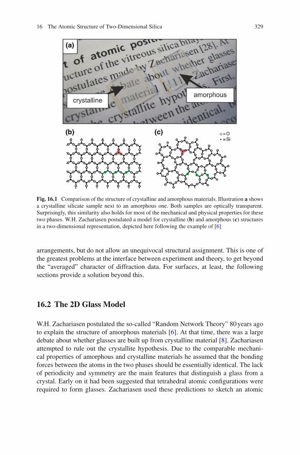
Figure16.1a illustrates how similar crystalline and amorphous samples can be.It shows a crystalline silicate, also called quartz, together with an amorphous sili-cate, i.e. a glass. The two samples exhibit many similar physical properties [7]. Forexample, due to very similar optical transparency, it is not possible to distinguishthe two states with simply the naked eye. But what is the difference between thesetwo phases? Comparative investigations of crystalline and amorphous silicon diox-ide samples were undertaken around a hundred years ago, almost as soon as theLaue method for the diffraction of X-ray or neutron beams on solid bodies had beendeveloped. These methods average over large sample volumes on the macroscopicscale and primarily provide information in reciprocal space. Crystalline samples pro-duce discrete diffraction patterns while glasses do not. The diffraction informationobtained from glasses can be compared with theoretical models of possible atomic
16 The Atomic Structure of Two-Dimensional Silica 329
Fig. 16.1 Comparison of the structure of crystalline and amorphous materials. Illustration a showsa crystalline silicate sample next to an amorphous one. Both samples are optically transparent.Surprisingly, this similarity also holds for most of the mechanical and physical properties for thesetwo phases. W.H. Zachariasen postulated a model for crystalline (b) and amorphous (c) structuresin a two-dimensional representation, depicted here following the example of [6]
arrangements, but do not allow an unequivocal structural assignment. This is one ofthe greatest problems at the interface between experiment and theory, to get beyondthe “averaged” character of diffraction data. For surfaces, at least, the followingsections provide a solution beyond this.
16.2 The 2D Glass Model
W.H. Zachariasen postulated the so-called “Random Network Theory” 80years agoto explain the structure of amorphous materials [6]. At that time, there was a largedebate about whether glasses are built up from crystalline material [8]. Zachariasenattempted to rule out the crystallite hypothesis. Due to the comparable mechani-cal properties of amorphous and crystalline materials he assumed that the bondingforces between the atoms in the two phases should be essentially identical. The lackof periodicity and symmetry are the main features that distinguish a glass from acrystal. Early on it had been suggested that tetrahedral atomic configurations wererequired to form glasses. Zachariasen used these predictions to sketch an atomic
330 C. Büchner et al.
picture of a glass. In his paper he reduced the three-dimensional (3D) picture into atwo dimensions (2D) analogy (Fig. 16.1b, c).
For silicon dioxide, the simplest structural unit in the 3Dcase is a SiO4 tetrahedron.If the complexity of the system is reduced from 3D to 2D, the simplest structuralunit for silicon dioxide changes from the SiO4 tetrahedron to a SiO3 triangle. Thered triangle in Fig. 16.1b, c marks the SiO3 building unit. In Fig. 16.1b these SiO3triangles are linked to each other as individual building blocks at fixed 180◦ angles,corresponding to a crystallinematerial. This creates long-range order and periodicity.
If the angle between these structural units varies, the building blocks can developan extended network with rings of different sizes. As can be seen in Fig. 16.1c,the uniform structural units are linked to each other at apparently random angles.Zachariasen drew a 2D diagram in which trigonal units are linked together to createthe amorphous network. Due to the large variety of Si–O–Si angles which bridgetwo neighboring building units, the glass structure lacks periodicity and long rangeorder.
The illustration of the atomic structure in Fig. 16.1c became the most widespreadpicture for glass. This model was compatible with the existing data from X-ray andneutron diffraction of amorphous materials. Therefore, these postulates were veryuseful in explaining diffraction experiments on glasses [9].
Although this model has been widely used to explain structures in amorphousmaterials, it has never been observed in real space before. Can a similar reductionof the 3D structure to a 2D model system also be realized and characterized experi-mentally?
16.3 The Realization of an Amorphous Model System
The “Chemical Physics” Department of the Fritz Haber Institute is developing andstudying model systems in the context of catalytically important processes. Ourmodel systems make it possible to depict part of the complexity of dispersed realcatalysts and investigate them by surface science tools. This involves producing thin,well-ordered oxide films onmetal single-crystal substrates, which can also be studiedunder the experimental conditions of surface physics.
The first steps in surface science studies are to determine where the atoms aresituated at the surface and to assign the different chemical species. In this context areduction of complexity is necessary, and thus model systems which allow for a highdegree of control over the preparation conditions are required.
In our department thin silicate films had already been specifically prepared backin 2000 [10] in order to be able to study catalytic surface reactions. The first studiesinvestigated silicate films on molybdenum single crystals [10]. More recent work forother metal substrates, including ruthenium [11, 12], has been presented. By usingdifferent metal single-crystal substrates it is possible to exert a crucial influence onthe growth of these thin silicate films. While on the molybdenum single crystalspredominantly crystalline films of monolayer thickness are formed, with ruthenium
16 The Atomic Structure of Two-Dimensional Silica 331
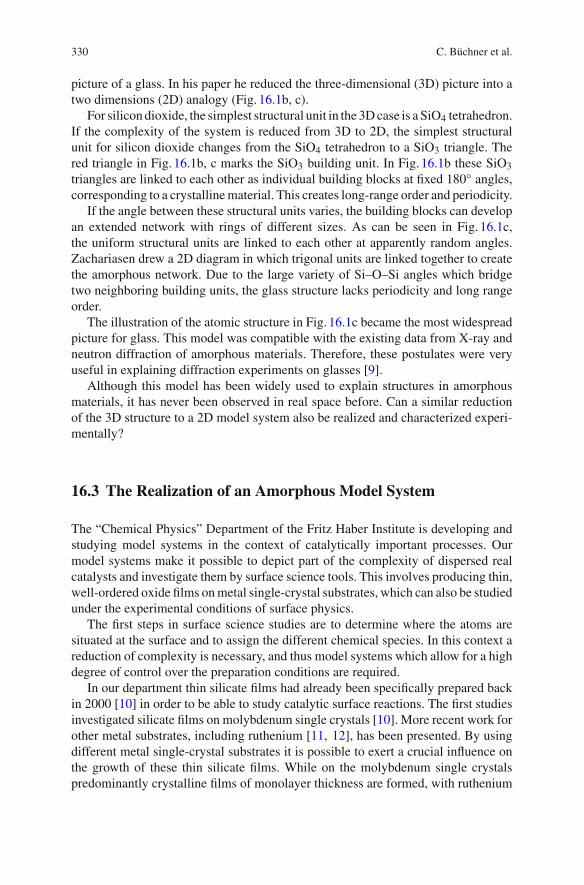
Fig. 16.2 Side view of the different silicate films with respect to different single-crystal substrate.a Silicate monolayer on a molybdenum single crystal [10], b silicate monolayer on a rutheniumsingle crystal, c silicate bilayer on a ruthenium single crystal [11, 12]
single crystals it is possible to specifically produce monolayers as well as bilayersilicate films. A detailed description of the sample preparation procedure can befound in [12].
Figure16.2 shows a side view of models for these film systems. In (a) and (b) themonolayer silicates have an oxygen back bonding to the underlying metal substrate.
In contrast, the bilayer film sketched in (c) is only weakly coupled to the metalsupport. Surprisingly, the bilayer silicate film on ruthenium single crystals can beproduced in crystalline [11] as well as amorphous structure [12]. The film’s registryto the underlying crystalline metal substrate can be lost. Thus, the film is structurallydecoupled from the metal support. This is evident from measurements with low-energy electron diffraction (LEED).
But can this model film system be used to observe the atomic structure directlyand thus corroborate the postulate of amorphous materials?
16.4 The Limits of Scanning Probe Methods
Today, there are promising new surface science tools available. During the lastdecades the development of scanning probe microscopy (SPM) has had a tremen-dous impact as an analytical tool to determine structural, spectroscopic as wellas dynamical aspects from all kinds of surfaces. Just a few years after its inven-tion by the group of Binnig and Rohrer, the scanning tunneling microscope (STM)[13, 14] turned into one of the most widely used surface analytical methods. In 1986,Quate together with Binnig presented the principle of the atomic force microscope(AFM) [15]. The AFM is an important addition to the STM, because it does notrequire conducting sample surfaces. However, it should be mentioned that it tookalmost ten more years to record atomically resolved images by AFM after its inven-tion [16]. Up to today the number of research groups working with advanced AFM
332 C. Büchner et al.
techniques, especially noncontact atomic force microscopy (nc-AFM), is relativelysmall compared to STM [17, 18].
SPM has been applied to a large variety of problems throughout the natural sci-ences, ranging from solid state physics to structural biology. Its cheap and relativelysimple design, and the large range of applications by SPM methods, make it a valu-able tool to study nature. SPM imaging can be done on a wide range of sampletypes, from atomically flat metal surfaces to living cells [19], and can be performedin vacuum, air, or liquid. This opens up a wide scope for experiments. Special setupswere developed for low [20–23], ultralow [24, 25] and variable-temperature studies[26, 27] in ultrahigh vacuum (UHV). Adaptations to perform measurements underhigh pressure [28], in liquids [29], at high speed [30, 31], time-resolved [32], or inmagnetic fields [33] have been conducted as well.
STM and AFM have been used extensively in the field of surface science tocharacterize surface morphology, structure, physical and chemical properties ofbulk and epitaxial samples [34]. The direct observation of molecular film structures[35, 36] as well as the recent achievements in resolving the chemical structure ofsingle molecules supported on flat crystals [37] are promising results. Besides thepure structural analysis, even individual atoms [38] and molecules [39, 40] weremanipulated by SPM.
Nevertheless, the atomic resolution of complex surface structures with large unitcells and individual defect network structures still remains a challenge, and only a fewexamples have been published [41]. The idea of characterizing amorphous surfacesbySTMwas proposed byWiesendanger et al. [42] in 1987. Since then,many attemptshave been made to atomically resolve amorphous materials, e.g. by SPM [43–48].However, this goal has never been achieved so far. An early measurements on glasssamples made by the research group of Klaus Wandelt and colleagues showed thepotential of these methods. However, it has been heavily debated, whether theseresults provide real atomic coordinates or not.
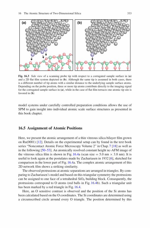
What is the reason behind this and what are the principle limitations of SPMmethods in general? These techniques often suffer from tip convolution effects [49].Slightly lower lying surface sites are often not imaged due to shielding effects of theneighboring atoms. In the case of corrugated sample surfaces a complicated convo-lution between tip and sample species takes place. The situation has been sketchedin Fig. 16.3 where the number of involved tip atoms is different for corrugated (a)compared to planar (b) sample surfaces.
Furthermore, it is often very demanding to separate electronic from topographicfeatures in STM [44], as well as to distinguish the chemical sensitivity of changingtip apexes towards different surface sites, both in STM and AFM. In a stable imagingmode typically only one type of species is imaged on the sample surface, either theanionic or the cationic site, depending on the actual tip configuration. However, ifthe probing tip apex is changing then this situation is hard to disentangle.
Clearly, a solution to these challenges is the reduction of dimensionality by usingwell defined thin film systems grownonmetal single crystalswhile retaining essentialaspects of the complexity of real systems. The growth of two-dimensionally flat
16 The Atomic Structure of Two-Dimensional Silica 333
Fig. 16.3 Side view of a scanning probe tip with respect to a corrugated sample surface in (a)and a 2D flat film system depicted in (b). Although the same tip is assumed in both cases, thereis a different number of tip atoms with a similar distance to the underlying sample surface atoms.Depending on the probe position, three or more tip atoms contribute directly to the imaging signalfor the corrugated sample surface in (a), while in the case of flat film terraces one atomic tip site isfavored in (b)
model systems under carefully controlled preparation conditions allows the use ofSPM to gain insight into individual atomic scale surface structures as presented inthis book chapter.
16.5 Assignment of Atomic Positions
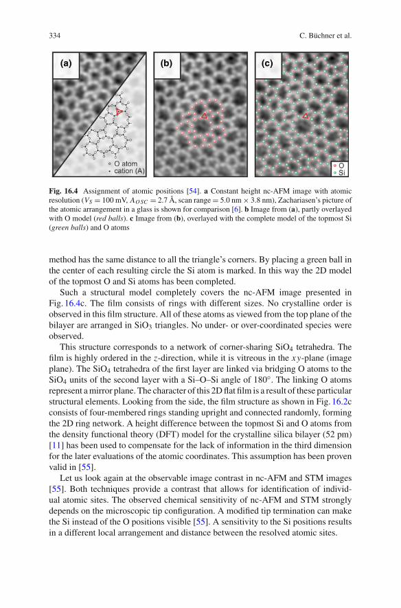
Here, we present the atomic arrangement of a thin vitreous silica bilayer film grownon Ru(0001) [12]. Details on the experimental setup can by found in the text bookseries “Noncontact Atomic Force Microscopy Volume 2” in Chap. 7 [18] as well asin the following [50–53]. An atomically resolved constant height nc-AFM image ofthe vitreous silica film is shown in Fig. 16.4a (scan size = 5.0 nm × 3.8 nm). It isuseful to look again at the postulates made by Zachariasen in 1932 [6], sketched forcomparison in the lower part of Fig. 16.4a. The complex atomic arrangement of this2D network film shows a striking similarity.
The observed protrusions at atomic separations are arranged in triangles. By com-paring to Zachariasen’s model and based on this triangular symmetry the protrusionscan be assigned to one face of a tetrahedral SiO4 building block. Consequently, theprotrusions correspond to O atoms (red balls in Fig. 16.4b). Such a triangular unithas been marked by a red triangle in Fig. 16.4.
Here, an O sensitive contrast is observed and the position of the Si atoms hasbeen calculated based on the O coordinates. The Si coordinates are determined usinga circumscribed circle around every O triangle. The position determined by this
334 C. Büchner et al.
Fig. 16.4 Assignment of atomic positions [54]. a Constant height nc-AFM image with atomicresolution (VS = 100 mV, AO SC = 2.7 Å, scan range = 5.0 nm × 3.8 nm), Zachariasen’s picture ofthe atomic arrangement in a glass is shown for comparison [6]. b Image from (a), partly overlayedwith O model (red balls). c Image from (b), overlayed with the complete model of the topmost Si(green balls) and O atoms
method has the same distance to all the triangle’s corners. By placing a green ball inthe center of each resulting circle the Si atom is marked. In this way the 2D modelof the topmost O and Si atoms has been completed.
Such a structural model completely covers the nc-AFM image presented inFig. 16.4c. The film consists of rings with different sizes. No crystalline order isobserved in this film structure. All of these atoms as viewed from the top plane of thebilayer are arranged in SiO3 triangles. No under- or over-coordinated species wereobserved.
This structure corresponds to a network of corner-sharing SiO4 tetrahedra. Thefilm is highly ordered in the z-direction, while it is vitreous in the xy-plane (imageplane). The SiO4 tetrahedra of the first layer are linked via bridging O atoms to theSiO4 units of the second layer with a Si–O–Si angle of 180◦. The linking O atomsrepresent amirror plane. The character of this 2Dflat film is a result of these particularstructural elements. Looking from the side, the film structure as shown in Fig. 16.2cconsists of four-membered rings standing upright and connected randomly, formingthe 2D ring network. A height difference between the topmost Si and O atoms fromthe density functional theory (DFT) model for the crystalline silica bilayer (52 pm)[11] has been used to compensate for the lack of information in the third dimensionfor the later evaluations of the atomic coordinates. This assumption has been provenvalid in [55].
Let us look again at the observable image contrast in nc-AFM and STM images[55]. Both techniques provide a contrast that allows for identification of individ-ual atomic sites. The observed chemical sensitivity of nc-AFM and STM stronglydepends on the microscopic tip configuration. A modified tip termination can makethe Si instead of the O positions visible [55]. A sensitivity to the Si positions resultsin a different local arrangement and distance between the resolved atomic sites.

16 The Atomic Structure of Two-Dimensional Silica 335
Fig. 16.5 a Sketch of the used tuning fork sensor device for nc-AFM/STM [52]. The STM tip iselectrically connected by a thin Pt/Rh wire with a diameter of 50 µm. Both the tip and Pt/Rh wireare insulated from the tuning fork and its electrodes. This is necessary to prevent a cross couplingbetween the nc-AFM and the STM signal. b, c Both images represent a single atomically resolvedconstant height measurement, where (b) shows the nc-AFM and (c) the STM channel. Imagingparameters b oscillation amplitude = 0.27 nm, gray scale from −1.0 (dark) to +0.6 Hz (bright); cVS = 100 mV, gray scale from 50 (dark) to 500 pA (bright); b, c scan area = 2.7 nm × 3.9 nm.In (b) the structure of the Si atoms is visible, whereas (c) reveals the arrangement of the O atoms.Also here an atomic model of the topmost layer of the silica film is superimposed onto the lowerright corner of the images in (b) and (c) (green balls Si atoms, red balls O atoms)
Our sensor device has the capability to directly combine nc-AFM and STM. Thisdevice is sketched in Fig. 16.5a. When the tip is probing the sample surface, wecan detect the interaction force and the tunneling current independently. Here, wecan simultaneously and at the same atomic site gather data about interaction forcesand electronic structure without cross-talk. Essentially we develop a more completeunderstanding of the surface by employing the full benefits of AFM and the fullbenefits of STM in parallel. These provide distinct, but complementary informationabout the surface.
This unique setup is capable of resolving clearly separated features from the sur-face in these two detection channels. Figure16.5b, c represent one single atomicallyresolved constant height nc-AFM and STMmeasurement above a vitreous region ofthe silica film. Figure16.5b is a map of the frequency shift (� f ), while Fig. 16.5c isthe simultaneously recorded map of the tunneling current (IT ). Both images show aring network with pores of various sizes. The power of this approach becomes clear ifwe take a closer look at the atomic structures that were resolved. While the � f -mapin Fig. 16.5b shows the Si positions (green balls), the IT -image in Fig. 16.5c revealsthe O positions (red balls) of the topmost silica layer.
In the top part of Fig. 16.5b, c this can be verified by looking at the nearestneighbor (NN) configurations of the imaged protrusions. In Fig. 16.5c the contrastin the STM signal is similar to nc-AFM image in Fig. 16.4. Every three protrusions(red balls) form a triangle representing one triangular side of an SiO4 tetrahedron.Therefore, these positions correspond to O atoms. However, in Fig. 16.5b, four pro-trusions (green balls) form a three-bladed windmill with one protrusions sitting in
336 C. Büchner et al.
its center. These positions represent the centers of four different tetrahedra and there-fore correspond to the Si atoms. Furthermore, the NN distances are characteristic fora certain atom type and are significantly larger for Si than for O. The structural infor-mation of both channels can be combined in this case to obtain a complete surfacemodel without any further assumptions as plotted in the bottom part of Fig. 16.5b, c.
Please note, that also combinations of nc-AFM and STM images have beenobserved in which the same surface species have been detected.
In the following analysis the atomically resolved nc-AFM image and the derivedmodel of the topmost layer from Fig. 16.4 has been used as a starting point for furtherevaluation of the thin film’s structure.
16.6 Atomic Force Microscopy Challenges X-RayDiffraction
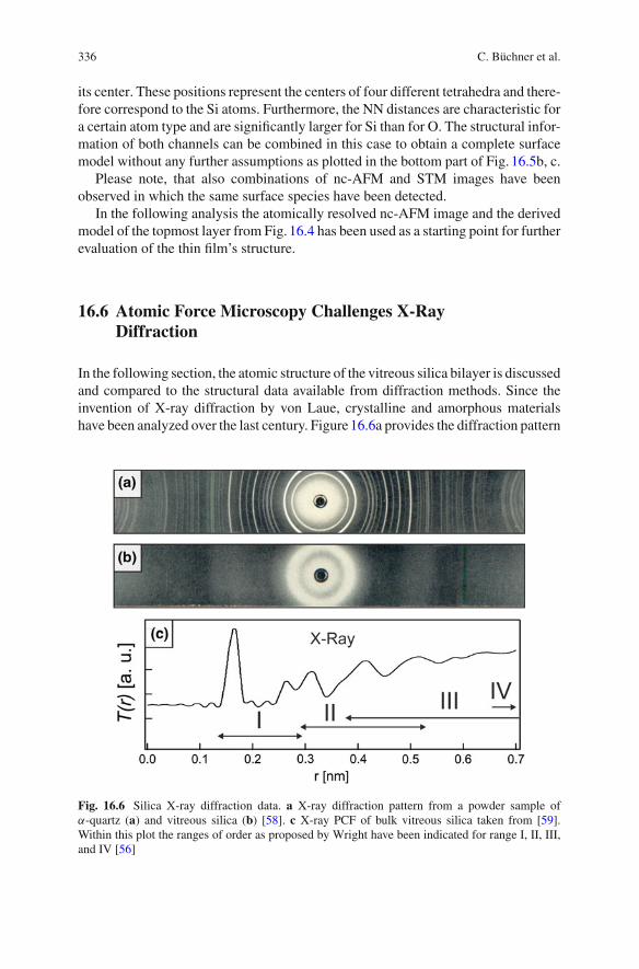
In the following section, the atomic structure of the vitreous silica bilayer is discussedand compared to the structural data available from diffraction methods. Since theinvention of X-ray diffraction by von Laue, crystalline and amorphous materialshave been analyzed over the last century. Figure16.6a provides the diffraction pattern
Fig. 16.6 Silica X-ray diffraction data. a X-ray diffraction pattern from a powder sample ofα-quartz (a) and vitreous silica (b) [58]. c X-ray PCF of bulk vitreous silica taken from [59].Within this plot the ranges of order as proposed by Wright have been indicated for range I, II, III,and IV [56]
16 The Atomic Structure of Two-Dimensional Silica 337
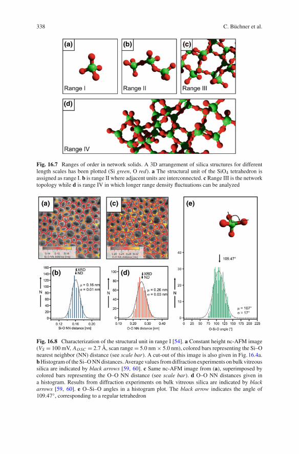
of a powder sample from α-quartz. Herein, the randomly oriented crystalline grainsin the powder produce a sharp ring pattern. The diffraction pattern of vitreous silicagiven in (b) only exhibits diffuse halos. Figure16.6c shows a typical pair correlationfunction derived from X-ray diffraction data from vitreous silica. A classificationintroduced by Wright, who divided the order in network solids in four ranges, isused. The following section is divided accordingly into the ranges: I structural unit,II interconnection of adjacent structural units, III network topology, and IV longerrange density fluctuations [56, 57].
In range I, the basic structural unit (SiO4 tetrahedron) is addressed and parametersfrom the X-ray PCF can be extracted by using peak fitting techniques. However,in ranges II and III, simple extraction of structural parameters is not possible andmodels are required for interpretations. In range II the interconnection and relativeorientationof twocorner-sharingSiO4 units is involved.Here, the variable parametersof the Si–O–Si bond angle and torsion angles can be defined. In this range the firstexample of disorder in comparison to crystallinemodification can be observed.RangeIII describes the network topology of amorphous network solids. In this range adescription of the first neighbors and shortest path statistics has always been desired,but has never been observed in real space before. In the literature a controversialdiscussion can be found, where theoretical models have been tested by comparisonto PCFs from XRD or ND. In range IV the long range density fluctuations areaddressed. However, the density differences between more and less ordered regionsare likely to be relative small. While there is quantitative knowledge about ranges Iand II, ranges III and IV are still much less understood and hence leave opportunitiesfor new developments.
The different orders are visualized by snapshots of atomic structures in Fig. 16.7.This classification turned out to be extremely useful to discuss and interpret thestructural information in diffraction experiments.
16.6.1 Structural Unit—Range I
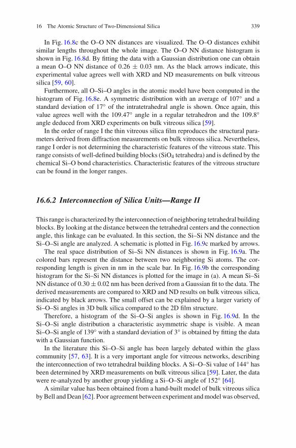
This range deals with the tetrahedron unit schematically drawn in the inset ofFig. 16.8e. A tetrahedron is primarily defined by the side length and the tetrahedralangle. The distance from the center to one corner is another characteristic parame-ter. With this respect the Si–O, the O–O distance, and the O–Si–O angle have beenanalyzed.
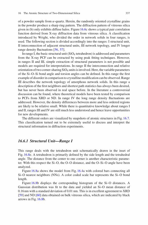
Figure16.8a shows the model from Fig. 16.4a with colored bars connecting allSi–O nearest neighbors (NNs). A color coded scale bar represents the Si–O bondlength.
Figure16.8b displays the corresponding histogram of the Si–O distances. AGaussian distribution was fit to the data and yielded an Si–O mean distance of0.16nm with a standard deviation of 0.01 nm. This is in excellent agreement to XRD[59] and ND [60] data obtained on bulk vitreous silica, which are indicated by blackarrows in Fig. 16.8b.
338 C. Büchner et al.
Fig. 16.7 Ranges of order in network solids. A 3D arrangement of silica structures for differentlength scales has been plotted (Si green, O red). a The structural unit of the SiO4 tetrahedron isassigned as range I. b is range II where adjacent units are interconnected. c Range III is the networktopology while d is range IV in which longer range density fluctuations can be analyzed
Fig. 16.8 Characterization of the structural unit in range I [54]. a Constant height nc-AFM image(VS = 100 mV, AO SC = 2.7 Å, scan range = 5.0 nm × 5.0 nm), colored bars representing the Si–Onearest neighbor (NN) distance (see scale bar). A cut-out of this image is also given in Fig. 16.4a.bHistogramof the Si–ONNdistances.Average values fromdiffraction experiments on bulk vitreoussilica are indicated by black arrows [59, 60]. c Same nc-AFM image from (a), superimposed bycolored bars representing the O–O NN distance (see scale bar). d O–O NN distances given ina histogram. Results from diffraction experiments on bulk vitreous silica are indicated by blackarrows [59, 60]. e O–Si–O angles in a histogram plot. The black arrow indicates the angle of109.47◦, corresponding to a regular tetrahedron
16 The Atomic Structure of Two-Dimensional Silica 339
In Fig. 16.8c the O–O NN distances are visualized. The O–O distances exhibitsimilar lengths throughout the whole image. The O–O NN distance histogram isshown in Fig. 16.8d. By fitting the data with a Gaussian distribution one can obtaina mean O–O NN distance of 0.26 ± 0.03 nm. As the black arrows indicate, thisexperimental value agrees well with XRD and ND measurements on bulk vitreoussilica [59, 60].
Furthermore, all O–Si–O angles in the atomic model have been computed in thehistogram of Fig. 16.8e. A symmetric distribution with an average of 107◦ and astandard deviation of 17◦ of the intratetrahedral angle is shown. Once again, thisvalue agrees well with the 109.47◦ angle in a regular tetrahedron and the 109.8◦angle deduced from XRD experiments on bulk vitreous silica [59].
In the order of range I the thin vitreous silica film reproduces the structural para-meters derived from diffraction measurements on bulk vitreous silica. Nevertheless,range I order is not determining the characteristic features of the vitreous state. Thisrange consists of well-defined building blocks (SiO4 tetrahedra) and is defined by thechemical Si–O bond characteristics. Characteristic features of the vitreous structurecan be found in the longer ranges.
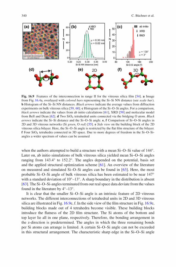
16.6.2 Interconnection of Silica Units—Range II
This range is characterized by the interconnection of neighboring tetrahedral buildingblocks. By looking at the distance between the tetrahedral centers and the connectionangle, this linkage can be evaluated. In this section, the Si–Si NN distance and theSi–O–Si angle are analyzed. A schematic is plotted in Fig. 16.9c marked by arrows.
The real space distribution of Si–Si NN distances is shown in Fig. 16.9a. Thecolored bars represent the distance between two neighboring Si atoms. The cor-responding length is given in nm in the scale bar. In Fig. 16.9b the correspondinghistogram for the Si–Si NN distances is plotted for the image in (a). A mean Si–SiNN distance of 0.30 ± 0.02 nm has been derived from a Gaussian fit to the data. Thederived measurements are compared to XRD and ND results on bulk vitreous silica,indicated by black arrows. The small offset can be explained by a larger variety ofSi–O–Si angles in 3D bulk silica compared to the 2D film structure.
Therefore, a histogram of the Si–O–Si angles is shown in Fig. 16.9d. In theSi–O–Si angle distribution a characteristic asymmetric shape is visible. A meanSi–O–Si angle of 139◦ with a standard deviation of 3◦ is obtained by fitting the datawith a Gaussian function.
In the literature this Si–O–Si angle has been largely debated within the glasscommunity [57, 63]. It is a very important angle for vitreous networks, describingthe interconnection of two tetrahedral building blocks. A Si–O–Si value of 144◦ hasbeen determined by XRD measurements on bulk vitreous silica [59]. Later, the datawere re-analyzed by another group yielding a Si–O–Si angle of 152◦ [64].
A similar value has been obtained from a hand-built model of bulk vitreous silicabyBell andDean [62]. Poor agreement between experiment andmodelwas observed,
340 C. Büchner et al.
Fig. 16.9 Features of the interconnection in range II for the vitreous silica film [54]. a Imagefrom Fig. 16.4a, overlayed with colored bars representing the Si–Si NN distance (see scale bar).b Histogram of the Si–Si NN distances. Black arrows indicate the average values from diffractionexperiments on bulk vitreous silica [59, 60]. c Histogram of the Si–O–Si angles. For a comparison,black arrows indicate the values from ab initio calculations [61], XRD [59] and molecular modelfrom Bell and Dean [62]. d Two SiO4 tetrahedral units connected via the bridging O atom. Blackarrows indicate the Si–Si distance and the Si–O–Si angle. e, f Comparison of Si–O–Si angles in2D and 3D vitreous networks (Si green, O red) [55]. e Side view on the building block of the 2Dvitreous silica bilayer. Here, the Si–O–Si angle is restricted by the flat film structure of the bilayer.f Four SiO4 tetrahedra connected in 3D space. Due to more degrees of freedom in the Si–O–Si-angles a wider spectrum of values can be assumed
when the authors attempted to build a structure with a mean Si–O–Si value of 144◦.Later on, ab initio simulations of bulk vitreous silica yielded mean Si–O–Si anglesranging from 143.4◦ to 152.2◦. The angles depended on the potential, basis setand the applied structural optimization scheme [61]. An overview of the literatureon measured and simulated Si–O–Si angles can be found in [63]. Here, the mostprobable Si–O–Si angle of bulk vitreous silica has been estimated to be near 147◦with a standard deviation of 10◦–13◦. A sharp boundary in the distribution is absent[63]. The Si–O–Si-angles terminated from our real space data deviate from the valuesfound in the literature by 4◦–13◦.
It is clear that the smaller Si–O–Si angle is an intrinsic feature of 2D vitreousnetworks. The different interconnections of tetrahedral units in 2D and 3D vitreoussilica are illustrated in Fig. 16.9e, f. In the side view of the film structure in Fig. 16.9e,building blocks made out of 4 tetrahedra become visible. These building blocksintroduce the flatness of the 2D film structure. The Si atoms of the bottom andtop layer lie all in one plane, respectively. Therefore, the bonding arrangement inthe z-direction is predetermined. The angles in which the three remaining bondsper Si atoms can arrange is limited. A certain Si–O–Si angle can not be exceededin this structural arrangement. The characteristic sharp edge in the Si–O–Si angle
16 The Atomic Structure of Two-Dimensional Silica 341
distribution of a 2D vitreous network visible in Fig. 16.9c can be assigned to thiseffect. In the 3D case, structures with a larger degree of freedom (f) are allowed(sketched in Fig. 16.9), resulting in a larger range of values for the Si–O–Si angles.In this range II, small but distinct differences due to the increased symmetry of thevitreous silica film structure have been observed in comparison to bulk silica. Thisincreased symmetry causes the film to be atomically flat, which allows us to tacklethe even more important range of the network topology, described in the followingsection.
16.6.3 Network Topology—Range III
This range of order is the most discussed and least understood topic in the glasscommunity. In this range the differences between crystals, with periodicity and order,and glass, with no periodicity and no order is most striking. In both phases theinitial buildings block are the same. The difference between a crystalline and a glassphase is in the relative orientation of these building blocks. A detailed comparison ofcrystalline and vitreous regions of the thin silica film is given in [55]. Characterizationof the larger radial distances, ring statistics, and Si–Si–Si angles have been evaluatedfor the thin silica film.
In direct comparison to diffraction data a PCF helps to characterize the atomicorder in amaterial. The computed long range distances for the silica film structure canbe compared to literature values. Radial pair distances for Si–O (blue), O–O (red),and Si–Si (green) measured from the nc-AFM model are indicated in Fig. 16.10a. Ahistogram of distances between all atoms in the model is plotted versus the radialdistance (r ) in the so called pair distance histograms (PDHs) in (b). Vertical coloredbars mark significant peak positions.
The first peaks in all three distributions correspond to the first respective NNdistances. The origin of these positions has been presented in Sects. 16.6.1 and 16.6.2.Second peaks of each curve represent the next NN distances.
The second peaks exhibit a larger background compared to the first peaks. Theyare broader and more diffuse, which is an intrinsic feature of the vitreous nature ofthe film. The first peaks represent order of ranges I and II introduced by the chemicalbonding of the building blocks. The following peaks are broader and characterizerange III.
By summing up the different PDHs using X-ray and neutron scattering factorsof Si and O according to the formula in [62, 65], total pair correlation functionsof the experimentally derived structural model, (Tnc-AFM(r)), have been obtained.Due to the 2D structure of the thin film, Tnc-AFM(r) was normalized by r−1. ThePCF obtained in an XRD experiment and ND measurements on bulk vitreous silicain Fig. 16.10c, d have been plotted together with the respective curves Tnc-AFM(r)
calculated for the silica film structure. Reasonable agreement with the XRD andND PCFs with Tnc-AFM(r) was achieved for the major peak positions, their relativemagnitudes and peak shapes. But as already indicated in the discussion of range II,

342 C. Büchner et al.
Fig. 16.10 Analysis of pair distance histograms and pair correlation functions of the silica filmin comparison to diffraction data [54]. a Cutout of a vitreous silica image with a superimposedatomic model. Colored bars indicate the types of distances that are evaluated in (b). b Pair distancehistograms (PDHs) derived from the nc-AFM image given in Fig. 16.4. Radial distances for Si–O(blue curve), O–O (red curve), and Si–Si (green curve) are plotted. Peaks are indicated by verticalcolored bars for first and second NN. c Comparison of the total PCF, Tnc-AFM(r) (orange curve),with the PCF obtained from X-ray diffraction measurements on bulk vitreous silica (black curvehas been retraced from [59]). d Comparison of Tnc-AFM(r) (orange curve) to results from ND onbulk vitreous silica (black curve has been retraced from [60]). The PDH peak positions are in linewith the respective colored bars from (b)
small deviations induced by the different dimensionality of the two systems are visi-ble. While the silica glass studied in diffraction experiments is 3D, the silica bilayeron Ru(0001) is 2D. Nevertheless, a good agreement between the PCFs obtained indiffraction studies of bulk vitreous silica and the vitreous silica film is achieved.
Looking at the ring size distribution of the thin vitreous silica film is another wayto characterize the network topology. From diffraction measurements and other aver-aging techniques such ring size distribution are not directly attainable. This quantitycan only be obtained from real space data and represents the biggest advantage thismodel system has to offer. The ring size s is defined as the number of Si atoms perring. These rings are quite large objects and therefore a large statistical sample isrequired. For this analysis the atomically resolved STM image in Fig. 16.11a hasbeen used. This particular STM image shows a sensitivity to the Si atoms in contrastto the nc-AFM image from Fig. 16.4, where O atoms are visualized. The sensitivityof the scanning probe is mainly dominated by the microscopic tip termination. Anoverview of different tip contrasts for this film system has been presented in [55].The lower right part of Fig. 16.11a is superimposed with the atomic model of thetopmost Si and O atoms. A complex ring network is revealed similar to Fig. 16.4c.

16 The Atomic Structure of Two-Dimensional Silica 343
Fig. 16.11 The 2D vitreous silica ring size distribution [55]. a Large scale STM image of thevitreous silica film with a sensitivity to Si sites (VS = 2 V, IT = 50 pA, scan range = 11.2nm ×6.6nm). Half of this image is superimposed by the atomic model of the topmost Si and O atoms.bVisualization of the ring size distribution in real space. The different rings are indicated by coloredpolygons. c Histogram of the ring size distribution from the STM image in (b). A log-normal fit tothe data is given by a red dashed curve. d A log-normal plot of the ring size distribution guided bya dashed line
Figure16.11b presents the real space visualization of the ring size distribution.The polygonal area spanned by the Si atoms has been color coded for every ring.The environment of a ring apears to depend on its size. Rings with more than six Siatoms tend to be surrounded by smaller rings. The possible angles inside an SiO4tetrahedron govern the ring arrangement.
In Fig. 16.11c a histogram of the ring sizes from the STM image is depicted. Thedistribution of rings ranges from four Si atoms to nine Si atoms. The most com-mon ring has six Si atoms. The distribution is asymmetric regarding the maximum.A log-normal behavior characterizes the ring size distribution of the vitreous film.Such analysis was first presented by James F. Shackelford and Brian D. Brown for anextended Zachariasen network [66]. Therein, they have also used a log-normal ringsize distribution to characterize the 2D random network. The connectivity require-ments of 2D random network seem to be the origin for the behavior of the ring sizedistribution [66]. The silica/Ru(0001) ring size distribution can be fitted by a log-normal function or a line in the log-normal plot (dashed lines in Fig. 16.11c, d) withgood agreement.

344 C. Büchner et al.
Surprisingly, the ring size distribution over several sample preparations, evenwithin a certain range of preparation conditions, have provided very similar distribu-tions for vitreous silica film regions. The properties of bulk glasses strongly dependon their preparation conditions and it is believed that these are presumably influ-enced through their ring size statistics. Thereby an important parameter seems to bethe fictive temperature from which the glass was quenched from the liquid state. Itis expected that the ring statistics would also depend on preparation parameters forthe silica film. However, our current preparation procedures seem to always yield anideal 2D glass configuration. Currently, we are only able to change the ratio betweencrystalline and vitreous regions in our sample systems by controlling the bilayercoverage.
From Fig. 16.11b Si–Si–Si angles can be computed. The internal structure of thering is guided by the Si–Si–Si angle. For four- to nine-membered rings histogramplots of the internal Si–Si–Si angles are shown in Fig. 16.12a–f. The correspondingedge angle of the regular polyhedron is marked by a black arrow for every ring size.Since the rings in the vitreous silica film can have a flexible shape, a broadening ofthe Si–Si–Si angle is observed. The mean value of each distribution, however, is ingood agreement with the ideal polyhedral angle. The sum of all ring contributionsis plotted in Fig. 16.13. The Si–Si–Si angle shows a broad distribution, having a
Fig. 16.12 Histograms of Si–Si–Si angles [55]. a–f Histograms of Si–Si–Si angles in four- tonine-membered rings are plotted separately. Internal angles of regular polyhedra are indicated byarrows and numbers at the top

16 The Atomic Structure of Two-Dimensional Silica 345
Fig. 16.13 Total Si–Si–Si angle distribution [55]. Comparison of the Si–Si–Si angle distributionfor different ring sizes. The ring sizes are colored correspondingly
Fig. 16.14 2D mass density analysis of the silica film [54]. The green wireframe corresponds tothe model from Fig. 16.11b. The white dashed box displays a bilayer slab used to calculate the 2Dmass density. Colored boxes represent the lateral variation of the 2D mass density (see scale bar)
maximum at 120◦ corresponding to the average edge angle inside the most frequent,i.e., sixfold, ring. The broadness of the distribution further shows how flexible this2D amorphous structure can be.
16.6.4 Density Fluctuations—Range IV
The data in Fig. 16.11b for this silica film allows us to address even range IV, wherethe long range mass density is evaluated. In Fig. 16.14 the 2D mass density has beenvisualized. The green wireframe was used as a model for the density determination.Under the wireframe, small colored boxes depict the local mass density in mg/m2.The boxes have dimensions of 0.34 nm × 0.30 nm. For each box the local mass
346 C. Büchner et al.
density from a 2 nm × 2 nm slab around it was calculated. One slab has beenindicated by a white dashed square. Its dimensions have been chosen to be largerthan a typical ring size. The 2D mass density varies from 1.46 to 1.83 mg/m2 andhas been color coded in the small boxes for each slab. In the calculated 2D massdensities the complete bilayer structure has been considered. Both the topmost SiO4tetrahedra and the lower ones have been taken into account.
A total 2D mass density of 1.65 mg/m2 has been calculated for the silica film.A pure crystalline phase of the silica bilayer has a slightly higher 2D mass densityof 1.68 mg/m2. Small local fluctuations of the 2D mass density are observed forthe vitreous film. This might be induced by the local ring environment. Larger ringshave a lower density than areas consisting of smaller rings. The center of the image isdominated by smaller rings (four to sevenfold) indicated by the higher mass density,while in the lower left corner larger rings with a lower density are observed. Thisevaluation is just a starting point for the range IV order. Further insights might begained by a detailed analysis of the ring size environments.
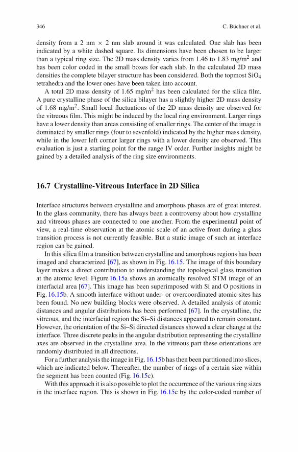
16.7 Crystalline-Vitreous Interface in 2D Silica
Interface structures between crystalline and amorphous phases are of great interest.In the glass community, there has always been a controversy about how crystallineand vitreous phases are connected to one another. From the experimental point ofview, a real-time observation at the atomic scale of an active front during a glasstransition process is not currently feasible. But a static image of such an interfaceregion can be gained.
In this silica film a transition between crystalline and amorphous regions has beenimaged and characterized [67], as shown in Fig. 16.15. The image of this boundarylayer makes a direct contribution to understanding the topological glass transitionat the atomic level. Figure16.15a shows an atomically resolved STM image of aninterfacial area [67]. This image has been superimposed with Si and O positions inFig. 16.15b. A smooth interface without under- or overcoordinated atomic sites hasbeen found. No new building blocks were observed. A detailed analysis of atomicdistances and angular distributions has been performed [67]. In the crystalline, thevitreous, and the interfacial region the Si–Si distances appeared to remain constant.However, the orientation of the Si–Si directed distances showed a clear change at theinterface. Three discrete peaks in the angular distribution representing the crystallineaxes are observed in the crystalline area. In the vitreous part these orientations arerandomly distributed in all directions.
For a further analysis the image in Fig. 16.15b has then been partitioned into slices,which are indicated below. Thereafter, the number of rings of a certain size withinthe segment has been counted (Fig. 16.15c).
With this approach it is also possible to plot the occurrence of the various ring sizesin the interface region. This is shown in Fig. 16.15c by the color-coded number of
16 The Atomic Structure of Two-Dimensional Silica 347
Fig. 16.15 2D structure ofa crystalline-amorphoustransition in a silica film [67].a STM image with atomicpositions marked. b Imagefrom (a) with color-codedrings to emphasize theirdistribution along thestructural transition fromcrystalline to amorphous.The change in the ring sizesfrom left to right is depictedin (c). The counts of ring sizeover the lateral position hasbeen determined. The purelycrystalline phase containsonly rings of 6; rings of 5and 7 first appear at thetransition, until the typicalring size distribution of theamorphous phase can beseen on the right
rings per slice. The various ring sizes do not occur at the same position in the interfaceregion. In fact, certain ring sizes occur simultaneously, and some combinations occurcloser to the crystal domain than others, as the interface region is entered from thecrystalline domain. Based on calculations of howmuch energy is necessary to changean arrangement of four six-membered rings into two five- and two seven-memberedrings versus two four- and two eight-membered rings, it turns out that the formercosts less energy than the latter. This is consistent with the general knowledge, thatthe Stone-Wales defect (a combination of five- and seven-membered rings) is thelowest energy defect in a hexagonal network [68].
Wooten and Weaire generated an early calculation of a crystalline-amorphousinterface for silicon [69]. In crystalline silicon the shortest-path rings of atoms are allsix-membered. By repeating random rearrangements of bonds, different ring sizeswere generated that lead to an amorphous phase. In the interface region between thecrystalline and amorphous phases, incorporation of five and sevenfold rings occurs.
348 C. Büchner et al.
This structural evolution is very similar to the one observed in our silica film.Huang et al. reported recently on the observation of structural rearrangements in
this amorphous silica bilayer film [70]. The authors used a probing electron beamof a transmission electron microscope (TEM) to deliberately cause rearrangements.Remarkable images and videos show the movements of structural building blocksat the atomic scale. The opening and closing of ring structures and the subsequentrearrangements can be directly observed. The results confirm our early models andDFT calculations [12] and open new ground for future modeling of dynamics inglasses. By providing the opportunity to study vitreous materials at the atomic level,this unique model system is likely to have great impact on the general understand-ing of dynamic processes in amorphous bulk materials. Future work might allow adirect assessment of atomic structures at the transition temperatures, where the liquidsolidifies to either the crystalline or the amorphous state.
16.8 Topological Analyzes of Two-Dimensional NetworkStructures
The presented advances in structural research allow one to search for a means ofnew classification for amorphous solids. Different concepts of classification andcomparisons encompassing a number of non-ordered natural and theoretical systemswere described in a milestone publication by Weaire and Rivier [71].
In a recent paper [72], the silica film structures in its crystalline and vitreous statewere compared to structural elements and configurations of other network structures,e.g., Si(111) 7×7 reconstruction [73], triangle rafts [66], amorphous graphene [74],copper oxide [75], molecular network structures [76], and bubble rafts [77, 78].
For all these networks, we can analyze real space structure data to determinecharacteristic properties and define descriptors of amorphous structures. The differ-ent network systems range from highly-ordered to completely unordered, includeexperiments and theoretical models, and span length scales from Ångströms to mil-limeters in bond length equivalents (Fig. 16.16).
All networks consist of rings that are defined by the number of comprised con-nection points (structural equivalents to Si atoms in the silica film). For each system,a ring size distribution with six-membered rings as the most abundant species canbe determined. By calculating the second and third central moment of each ringsize probability distribution, the variance and the skewness of a distribution can becaptured in one number and allow for quick comparison.
The ring size probability can also be plotted versus the ring size on a logarithmicaxis. This lognormal probability plot was suggested by Shackelford and Brown [66].They postulated that a lognormal ring size distribution is inherent to all amorphousnetworks. We find that this is true except for the network formed by the bubble raft.

16 The Atomic Structure of Two-Dimensional Silica 349
Fig. 16.16 Comparison of different network structures. Connection points in the center of theoccurring ring structures are marked with small green circles. Different sized rings are indicatedwith respective colors and partially superimposed onto the images. a Model of a Si(111) surface inthe 7× 7 reconstruction [73]. A rhombus shape indicates the unit cell. Si positions are marked withsmall green circles, different ring sizes are marked in different colors on part of the model. Five-,six- and eight-membered rings, occur in this complex crystalline surface. The unit cell also containsone 12-membered ring. b STM image of a crystalline SiO2 sheet (taken from [55]). The contrastreveals the Si positions of the SiO2 film, which are partly marked with small green circles. Six-membered rings (marked with large green circles on part of the image) are the only ring size in thishighly ordered system. c nc-AFM image reveals the atomic structure of an amorphous SiO2 bilayer[72]. Four- to nine-membered rings occur, six-membered rings exhibit the highest occurrence. d Acomputational model for a sheet of amorphous graphene [74]. On part of the image, C positionsare indicated with small green circles and different ring sizes are shown with colored circles. Inaddition to the five- to nine-membered rings also two 12-membered rings occur. e STM image of adefect-rich Cu2O(111) surface is shown [75]. It is partly superimposed with small green spheres atthe O positions and colored circles indicating polygon size. In the Cu2O, only five-, six- and seven-membered rings are observed. f STM image of an amorphous film of polymerized TBPB-Moleculeson a Au(111) substrate [76]. The molecule centers constitute the connection points of the resultingamorphous network, markedwith small green circles. Rings from four to eight connection points areobserved. g The image shows a triangle raft suggested by J. Shackelford as a model for amorphousSiO2 networks [66]. The algorithm for creating the triangle raft limits possible ring sizes from fourto eight. h Photo of a macroscopic bubble raft. Soap bubbles form a space-filling arrangement thatexhibits different sized polygons (shown with colored circles) and lacks long-range order. Ringsizes from four to eight are observed

350 C. Büchner et al.
This deviation is attributed to the larger variation in connection point distances, sincethe formation is not governed by chemical bond length or angle limitations.
Diffraction techniques yield total pair correlation functions including all atomicpositions.An advantage of real space information is the possibility to discern betweendifferent species. Atomic position data were used to create partial pair correlationfunctions of the connection points. They allow conclusions regarding characteristicbuilding unit distances and degree of order in the system. All systems exhibit similarcharacteristic bond distances far beyond the primary tetrahedral building block.
An additional benefit of real space information is the information regarding net-work topology over a larger scale. Several preferred arrangements of ring sizes havebeen identified as characteristic larger building units. They all consist of four ringsin a cluster of the sequence A-B-B-A with two rings of size B sharing two Si-atomsand a ring of size A on either side, sharing one of those Si atoms, respectively. Theoccurrence of the 5-7-7-5, 7-5-5-7, the 5-8-8-5 and the 8-5-5-8 clusters have beenanalyzed and their occurrence probability is in line with a qualitative model of ringstrain.
These different approaches at structure analysis can serve as a starting point fordiscussing and comparing unordered network structures in the future.
16.9 Summary
This vitreous silica model system, which can be investigated by well-establishedsurface science tools, provides the unique possibility to study an amorphous modelsystem with atomic resolution in real space.
The structure of this atomically flat and extended vitreous silica film on Ru(0001)has been presented. nc-AFM/STM revealed the thin film’s atomic arrangement con-sisting of corner-sharing SiO4 units. These silica building blocks form a complexnetwork which lacks long-range order and registry to the substrate. This model sys-tem corroborates Zachariasen’s predictions of a random network theory for glassstructures. An atomic model of the topmost Si and O atoms has been directly derivedfrom nc-AFM/STM images. The atomic structure has been discussed in the follow-ing ranges: the SiO4 tetrahedral unit, interconnection of adjacent structural units,network topology, and longer range density fluctuations. Distances, angles, PCFsand histograms of ring sizes were given. A comparison between the PCF derivedfrom our experimental model and the PCF obtained in diffraction experiments onbulk vitreous silica was drawn and showed satisfying agreement.
The behavior of the ring size distribution at a crystalline-vitreous interface wasinvestigated. A gradual and smooth transition at the interface was found, wherefive and sevenfold rings occur closer to the crystalline region than four-, eight-, andnine-membered rings.
Certainly, such structural studies are a step forward in developing of a compre-hensive framework for understanding amorphous networks.

16 The Atomic Structure of Two-Dimensional Silica 351
In future experiments, the aim is to directly follow glass-formation phenomena.A possible route to do so is the application of the spectro-microscope SMART(spectro-microscope with aberration correction for many relevant techniques) [79]that was installed at the BESSY II (Berliner Elektronen-Speicherring-Gesellschaftfür Synchrotronstrahlung) electron storage ring. This instrument enables for real-time observation of layer growth, structure formation, diffusion and reaction frontsas well as phase transitions. Future work might allow for a direct assessment ofatomic structures at transition temperatures, where the liquid solidifies to either thecrystalline or the amorphous state. In current experiments, the preparation of thisunique silica film is adapted to the SMART setup. But also certain designs of SPMspresented in the literature have been shown to be, in principle, capable of followingatomic motions at elevated temperature. Results from such machines may open newroom for modeling the dynamics in glasses [80]. Studying vitreous materials at thisscale will have a great impact on the general understanding of dynamic processes inamorphous bulk materials [3].
The silica filmmight also be used in the context of Cr-doped porous silica glass asa model material to describe Phillips catalyst properties [81]. Doping [82], additionalgrowth [83], adsorption, and chemical reactivity [84] studies on this silica based filmsystem are still the focus of ongoing experiments.
It should be mentioned that these silica films can be grown on various substrates[12, 85–87],which leaves room for the possibility of a completely newmaterials classof its own. Band structure measurements or other materials properties of this silicafilm might reveal unexpected features similar to those of graphene. This film mayeven find applications as a new gatematerial in the semiconductor industry. However,this strongly depends on the final stability and properties of this film system.
To conclude, by this work our understanding of oxide surface structures andcomplex materials, e.g., amorphous solids, was significantly enhanced owing to theuse of high-resolution imaging and spectroscopy by SPM. The presented work canbe referenced as a stepping-stone for future studies.
Acknowledgments The authors would like to thank Hans-Peter Rust and Gero Thielsch for majorcontributions to the development and maintenance of the experimental setup. Furthermore, wewould like to acknowledge Kristen Burson, Thomas König, Georg Hermann Simon and StefanieStuckenholz for fruitful discussions.
References
1. S. Sastry, P.G. Debenedetti, F.H. Stillinger, Nature 393, 554 (1998)2. R. Zallen, The Physics of Amorphous Solids (Wiley-VCH Verlag GmbH & Co. KGaA, Wein-
heim, 2004)3. L. Berthier, G. Biroli, Rev. Mod. Phys. 83, 587 (2011)4. Corning Incorporated, One Riverfront Plaza Corning, NY 14831 USA5. P.G. Debenedetti, F.H. Stillinger, Nature 410, 259 (2001)6. W.H. Zachariasen, J. Am. Chem. Soc. 54, 3841 (1932)7. M. Wuttig, Phys. Status Solidi B 249, 1843 (2012)
352 C. Büchner et al.
8. J.T. Randall, H.P. Rooksby, B.S. Cooper, Z. Krist 75, 196 (1930)9. B.E. Warren, J. Am. Ceram. Soc. 17, 249 (1934)10. T. Schroeder, M. Adelt, B. Richter, M. Naschitzki, M. Bäumer, H.-J. Freund, Surf. Rev. Lett.
7, 7 (2000)11. D. Löffler, J.J. Uhlrich, M. Baron, B. Yang, X. Yu, L. Lichtenstein, L. Heinke, C. Büchner,
M. Heyde, S. Shaikhutdinov, H.-J. Freund, R. Włodarczyk, M. Sierka, J. Sauer, Phys. Rev.Lett. 105, 146104 (2010)
12. L. Lichtenstein, C. Büchner, B. Yang, S. Shaikhutdinov, M. Heyde, M. Sierka, R. Włodarczyk,J. Sauer, H.-J. Freund, Angew. Chem. Int. Ed. 51, 404 (2012)
13. G. Binnig, H. Rohrer, Helv. Phys. Acta 55, 726 (1982)14. G. Binnig, H. Rohrer, C. Gerber, E. Weibel, Phys. Rev. Lett. 49, 57 (1982)15. G. Binnig, C.F. Quate, C. Gerber, Phys. Rev. Lett. 56, 930 (1986)16. F.J. Giessibl, Science 267, 68 (1995)17. S. Morita, R. Wiesendanger, E. Meyer (eds.), Noncontact Atomic Force Microscopy (Springer,
Berlin, 2002)18. S. Morita, R. Wiesendanger, F.J. Giessibl (eds.), Noncontact Atomic Force Microscopy, vol 2
(Springer, Berlin, 2009)19. W.Häberle, J. Hörber, F. Ohnesorge, D. Smith, G. Binnig, Ultramicroscopy 42–44, 1161 (1992)20. S.A. Elrod, A.L. de Lozanne, C.F. Quate, Appl. Phys. Lett. 45, 1240 (1984)21. D.P.E. Smith, G. Binnig, Rev. Sci. Instrum. 57, 2630 (1986)22. G. Meyer, Rev. Sci. Instrum. 67, 2960 (1996)23. C. Wittneven, R. Dombrowski, S.H. Pan, R. Wiesendanger, Rev. Sci. Instrum. 68, 3806 (1997)24. S.H. Pan, E.W. Hudson, J.C. Davis, Rev. Sci. Instrum. 70, 1459 (1999)25. M. Kugler, C. Renner, Ø. Fischer, V. Mikheev, G. Batey, Rev. Sci. Instrum. 71, 1475 (2000)26. J.W. Lyding, S. Skala, J.S. Hubacek, R. Brockenbough, G. Gammie, Rev. Sci. Instrum. 59,
1897 (1988)27. B.C. Stipe, M.A. Rezaei, W. Ho, Rev. Sci. Instrum. 70, 137 (1999)28. B.J. McIntyre, M. Salmeron, G.A. Somorjai, Rev. Sci. Instrum. 64, 687 (1993)29. F. Ohnesorge, G. Binnig, Science 260, 1451 (1993)30. J. Wintterlin, J. Trost, S. Renisch, R. Schuster, T. Zambelli, G. Ertl, Surf. Sci. 394, 159 (1997)31. M.J. Rost, L. Crama, P. Schakel, E. van Tol, G.B.E.M. van Velzen-Williams, C.F. Overgauw,
H. ter Horst, H. Dekker, B. Okhuijsen, M. Seynen, A. Vijftigschild, P. Han, A.J. Katan,K. Schoots, R. Schumm, W. van Loo, T.H. Oosterkamp, J.W.M. Frenken, Rev. Sci. Instrum.76, 0537101 (2005)
32. A. Bryant, D.P.E. Smith, C.F. Quate, Appl. Phys. Lett. 48, 832 (1986)33. R. Wiesendanger, Rev. Mod. Phys. 81, 1495 (2009)34. C.J. Chen, Introduction to Scanning Tunneling Microscopy (Oxford University Press, Oxford,
2009)35. J.P. Rabe, S. Buchholz, Science 253, 424 (1991)36. J.P. Rabe, S. Buchholz, Phys. Rev. Lett. 66, 2096 (1991)37. L. Gross, F. Mohn, N. Moll, P. Liljeroth, G. Meyer, Science 325, 1110 (2009)38. D.M. Eigler, E.K. Schweizer, Nature 344, 524 (1990)39. S.-W. Hla, L. Bartels, G. Meyer, K.-H. Rieder, Phys. Rev. Lett. 85, 2777 (2000)40. D.G. de Oteyza, P. Gorman, Y.-C. Chen, S. Wickenburg, A. Riss, D.J. Mowbray, G. Etkin,
Z. Pedramrazi, H.-Z. Tsai, A. Rubio, M.F. Crommie, F.R. Fischer, Science 340, 1434 (2013)41. J.V. Lauritsen, M. Reichling, J. Phys. Condens. Matter 22, 263001 (2010)42. R. Wiesendanger, M. Ringger, L. Rosenthaler, H. Hidber, P. Oelhafen, H. Rudin,
H.-J. Güntherodt, Surf. Sci. 181, 46 (1987)43. W. Raberg, K. Wandelt, Appl. Phys. A Mater. Sci. Process. 66, 1143 (1998)44. D.E. Bürgler, C.M. Schmidt, D.M. Schaller, F. Meisinger, T.M. Schaub, A. Baratoff,
H.-J. Güntherodt, Phys. Rev. B 59, 10895 (1999)45. H. Schlenz, A. Kirfel, K. Schulmeister, N. Wartner, W. Mader, W. Raberg, K. Wandelt,
C. Oligschleger, S. Bender, R. Franke, J. Hormes, W. Hoffbauer, V. Lansmann, M. Jansen,N. Zotov, C. Marian, H. Putz, J. Neuefeind, J. Non-Cryst. Solids 297, 37 (2002)
16 The Atomic Structure of Two-Dimensional Silica 353
46. J.-F. Poggemann, G. Heide, G. Frischat, J. Non-Cryst. Solids 326–327, 15 (2003)47. G. Frischat, J.-F. Poggemann, G. Heide, J. Non-Cryst. Solids 345–346, 197 (2004)48. W. Raberg, A. Ostadrahimi, T. Kayser, K. Wandelt, J. Non-Cryst. Solids 351, 1089 (2005)49. J.S. Villarrubia, J. Res. Nat. Inst. Stand. Technol. 102, 425 (1997)50. M. Heyde, M. Kulawik, H.-P. Rust, H.-J. Freund, Rev. Sci. Instrum. 75, 2446 (2004)51. H.-P. Rust, M. Heyde, H.-J. Freund, Rev. Sci. Instrum. 77, 043710 (2006)52. M. Heyde, G.H. Simon, H.-P. Rust, H.-J. Freund, Appl. Phys. Lett. 89, 263107 (2006)53. T. König, G.H. Simon, L. Heinke, L. Lichtenstein, M. Heyde, Beilstein J. Nanotechnol. 2, 1
(2011)54. M. Heyde, G.H. Simon, L. Lichtenstein, Phys. Status Solidi B 250, 895 (2013)55. L. Lichtenstein, M. Heyde, H.-J. Freund, J. Phys. Chem. C 116, 20426 (2012)56. A.C. Wright, J. Non-Cryst. Solids 106, 1 (1988)57. A.C. Wright, J. Non-Cryst. Solids 179, 84 (1994)58. H.S. Peiser, H.P. Rooksby,A.J.C.Wilson (eds.), X-RayDiffraction by PolycrystallineMaterials
(Institute of Physics, London, 1955)59. R.L. Mozzi, B.E. Warren, J. Appl. Crystallogr. 2, 164 (1969)60. D.I. Grimley, A.C. Wright, R.N. Sinclair, J. Non-Cryst. Solids 119, 49 (1990)61. R.M. Van Ginhoven, H. Jónsson, L.R. Corrales, Phys. Rev. B 71, 024208 (2005)62. R.J. Bell, P. Dean, Philos. Mag. 25, 1381 (1972)63. X. Yuan, A. Cormack, J. Non-Cryst. Solids 319, 31 (2003)64. J.R.G. Da Silva, D.G. Pinatti, C.E. Anderson, M.L. Rudee, Philos. Mag. 31, 713 (1975)65. L. Gladden, J. Non-Cryst. Solids 119, 318 (1990)66. J.F. Shackelford, B.D. Brown, J. Non-Cryst Solids 44, 379 (1981)67. L. Lichtenstein, M. Heyde, H.-J. Freund, Phys. Rev. Lett. 109, 106101 (2012)68. A. Stone, D. Wales, Chem. Phys. Lett. 128, 501 (1986)69. F. Wooten, D. Weaire, J. Non-Cryst. Solids 144(Part 2), 681 (1989)70. P.Y. Huang, S. Kurasch, J.S. Alden, A. Shekhawat, A.A. Alemi, P.L. McEuen, J.P. Sethna,
U. Kaiser, D.A. Muller, Science 342, 224 (2013)71. D. Weaire, N. Rivier, Contem. Phys. 50, 199 (2009)72. C. Büchner, P. Schlexer, L. Lichtenstein, S. Stuckenholz, M. Heyde, H.-J. Freund, Zeitschrift
für Physikalische Chemie 228, 587 (2014)73. K. Takayanagi, Y. Tanishiro,M. Takahashi, S. Takahashi, J. Vac. Sci. Technol. A 3, 1502 (1985)74. Y. Li, D.A. Drabold, Phys. Status Solidi B 250, 1012 (2013)75. F. Yang, Y. Choi, P. Liu, D. Stacchiola, J. Hrbek, J.A. Rodriguez, J. Am. Chem. Soc. 133,
11474 (2011)76. M.O. Blunt, J.C. Russell, N.R. Champness, P.H. Beton, Chem. Commun. 46, 7157 (2010)77. L. Bragg, J.F. Nye, Naturwissenschaften 34, 328 (1947)78. L. Bragg, J.F. Nye, Proc. R. Soc. Lond. Ser. A. Math. Phys. Sci. 190, 474 (1947)79. R. Fink, M. Weiss, E. Umbach, D. Preikszas, H. Rose, R. Spehr, P. Hartel, W. Engel,
R. Degenhardt, R. Wichtendahl, H. Kuhlenbeck, W. Erlebach, K. Ihmann, R. Schlögl, H.-J.Freund, A. Bradshaw, G. Lilienkamp, T. Schmidt, E. Bauer, G. Benner, J. Electron Spectrosc.Relat. Phenom. 84, 231 (1997)
80. P.W. Anderson, Proc. Natl. Acad. Sci. 92, 6653 (1995)81. A. Budnyk, A. Damin, C. Barzan, E. Groppo, C. Lamberti, S. Bordiga, A. Zecchina, J. Catal.
308, 319 (2013)82. J.A. Boscoboinik, X. Yu, B. Yang, F.D. Fischer, R. Włodarczyk, M. Sierka, S. Shaikhutdinov,
J. Sauer, H.-J. Freund, Angew. Chem. Int. Ed. 51, 6005 (2012)83. B. Yang, W.E. Kaden, X. Yu, J.A. Boscoboinik, Y. Martynova, L. Lichtenstein, M. Heyde,
M. Sterrer, R. Włodarczyk, M. Sierka, J. Sauer, S. Shaikhutdinov, H.-J. Freund, Phys. Chem.Chem. Phys. 14, 11344 (2012)
84. J.A. Boscoboinik, X. Yu, E. Emmez, B. Yang, S. Shaikhutdinov, F.D. Fischer, J. Sauer,H.-J. Freund, J. Phys. Chem. C 117, 13547 (2013)
85. X. Yu, B. Yang, J.A. Boscoboinik, S. Shaikhutdinov, H.-J. Freund, Appl. Phys. Lett. 100,151608 (2012)
86. P.Y. Huang, S. Kurasch, A. Srivastava, V. Skakalova, J. Kotakoski, A.V. Krasheninnikov,R. Hovden, Q. Mao, J.C. Meyer, J. Smet, D.A. Muller, U. Kaiser, Nano Lett. 12, 1081 (2012)
87. E.I. Altman, U.D. Schwarz, Adv. Mater. Interf. 1, 1400108 (2014)


![Chapter 2 Atomic Scale Characterization of Defects on ...w0.rz-berlin.mpg.de/hjfdb/pdf/714e.pdf · of metal nano particles with oxide surfaces [5]. The most important one is the nature,](https://img.pdfslide.net/doc/110x75/5f066a377e708231d417e0ed/chapter-2-atomic-scale-characterization-of-defects-on-w0rz-of-metal-nano-particles.jpg)


![Atomic Defects in Two Dimensional Materialsresearch.physics.berkeley.edu › ... › pdf › ...Materials.pdf · materials. [ 10,11 ] Several advances have been critical in the fi](https://img.pdfslide.net/doc/110x75/5f0303057e708231d40719df/atomic-defects-in-two-dimensional-a-a-pdf-a-materialspdf-materials.jpg)


![Theoretical study of gapless low-dimensional systems ... · Almost at the same time of the discovery of graphene, low-dimensional systems became available in cold atomic systems [12]](https://img.pdfslide.net/doc/110x75/5e09a7695f5781099b5f0c3e/theoretical-study-of-gapless-low-dimensional-systems-almost-at-the-same-time.jpg)