Embed Size (px)
Citation preview
Chapter 2: Hardware Design Flow Using Verilog in Quartus II
2.1 Introduction to Quartus II System Development Software
This chapter is an introduction to the Quartus II software that will be used for analysis
and synthesis of the DE2-115 Development and Education Board. Throughout this chapter
hardware description languages like Verilog will be used for coding. The Altera Quartus II
design software provides a complete, multiplatform design environment for system-on-a-
programmable-chip (SOPC) designs. Also an example will be implemented in a tutorial using the
hardware description language (Verilog) and the DE2-115. Below are some suggested readings
before going into the next section.
Quartus II Development Software Reading Resources:
(In suggested chronological reading/watching order)
1) Introduction to Quartus II Software
Version 11.0 (Latest):
http://www.altera.com/literature/manual/quartus2_introduction.pdf
• NOTE: The link to the newer version of the later version (11.0) provides a very
brief overview, whereas the older version (listed below) gives more in depth information.
Version 10.0:
http://www.altera.com/literature/manual/archives/intro_to_quartus2.pdf
• focus: Emphasis is placed on the following sections, although a greater
knowledge base is achieved by reviewing the entire document:
a) Design Flow- Introduction (Page No. 11), Graphical User Interface Design
Flow (Page No. 12)
b) Design Entry (Page No. 29) Introduction, Creating a Project(Page No. 30),
Creating a Design(Page No. 31), later this document can be used for a specific
method of design entry (like Verilog, Block Diagram, VHDL, etc.)
c) Programming & Configuration (Page No. 93) Introduction, Creating and
Using Programming Files
2) Using Verilog for Quartus II Design:
<system cd>\DE2_115_tutorials\tut_quartus_intro_verilog.pdf
• focus: This tutorial guides through the simulation process so that the project can
be implemented without needing access to the DE2-115.(familiar with quartus and Verilog)
(PG No 1-21)
3) Quartus II Handbook: http://www.altera.com/literature/hb/qts/quartusii_handbook.pdf
• NOTE: This resource is in depth and is only necessary to briefly overview the
material in order to know where information can be found on an as needed basis.
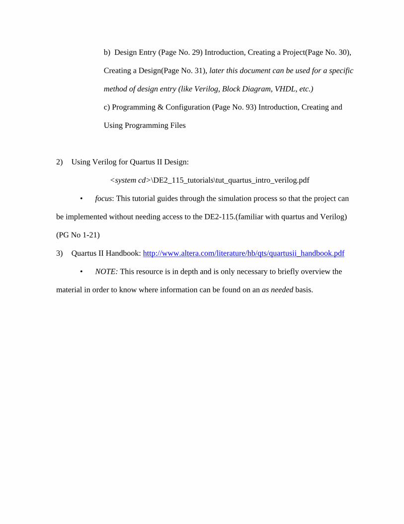
2.2 Design Flow (Hardware Only)
Design Entry
Synthesis
Timing Analysis and Simulation
Functional Simulation
Programming and Configuration
Fitting
Design correct?
Timing requirement met?
No
Yes
No
Yes
2.3 Binary Adder Example
Now that you are getting familiar with Quartus II and the DE2-11 a tutorial discussing
the basic steps for using Quartus II is discussed below.
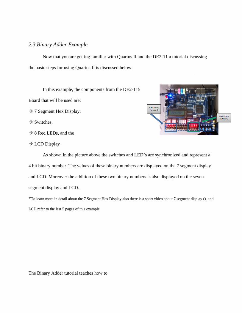
In this example, the components from the DE2-115
Board that will be used are:
7 Segment Hex Display,
Switches,
8 Red LEDs, and the
LCD Display
As shown in the picture above the switches and LED’s are synchronized and represent a
4 bit binary number. The values of these binary numbers are displayed on the 7 segment display
and LCD. Moreover the addition of these two binary numbers is also displayed on the seven
segment display and LCD.
*To learn more in detail about the 7 Segment Hex Display also there is a short video about 7 segment display () and
LCD refer to the last 5 pages of this example
The Binary Adder tutorial teaches how to

Connect the conputer with the DE2-115.
Create a new project using Quartus II.
Create a Verilog file.
Put I/O pin locations in the assignment editor.
Synthesize your design.
Use system builder.
1. The youtube video for the complete procedure can be accessed from the link given below:
http://www.youtube.com/watch?v=rpFxGuRB0xk
2. The example can also be implemented by using the written instructions given below:
Binary Adder Tutorial
Step 1: Install the USB driver for the FPGA development board. This step will only be
done for the first time the FPGA board is used.
a) On the FPGA board, connect the power plug to an outlet. Connect the USB cable
from your computer to the FPGA board in port J9 (closest to the power outlet).
b) Open the start Menu and Search Windows for “Device Manager”-> Scroll down
to “Other Devices”-> A new window called “USB Blaster Properties” will open.

c) Under the tab “Driver” select “Update Driver” -> A new window will pop up and
you’ll select “Browse my computer for driver software
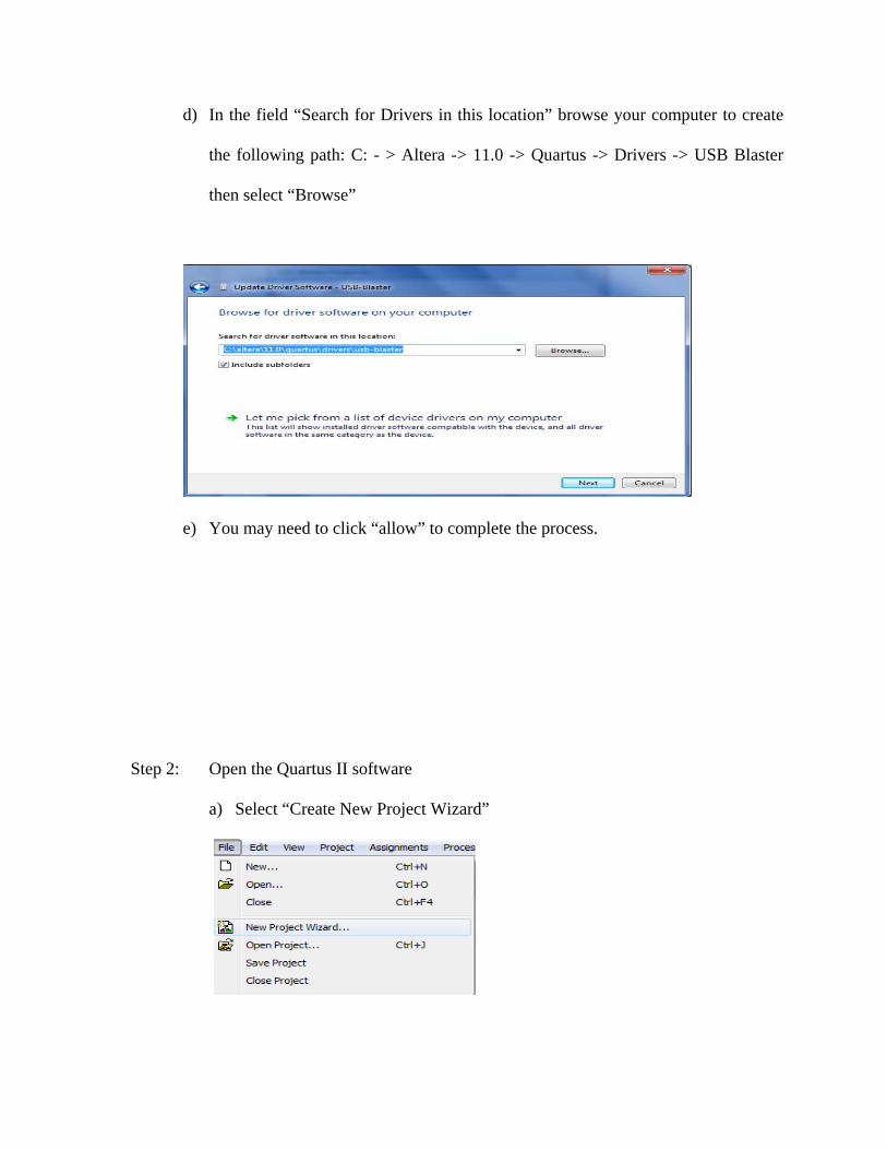
d) In the field “Search for Drivers in this location” browse your computer to create
the following path: C: - > Altera -> 11.0 -> Quartus -> Drivers -> USB Blaster
then select “Browse”
e) You may need to click “allow” to complete the process.
Step 2: Open the Quartus II software
a) Select “Create New Project Wizard”
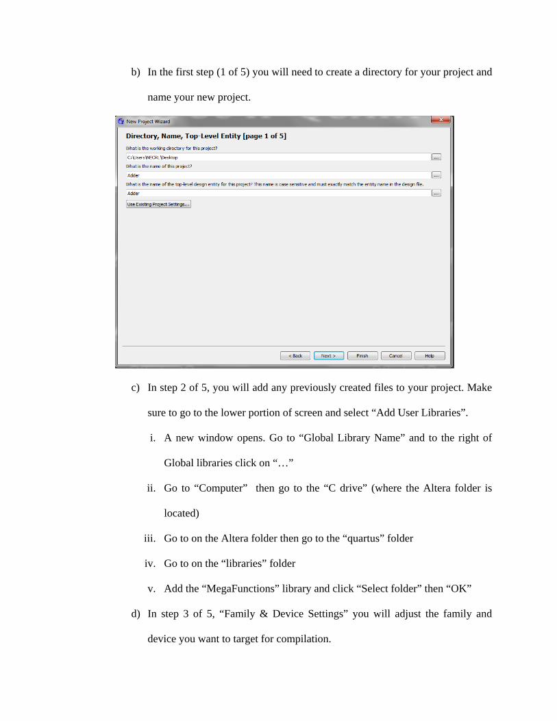
b) In the first step (1 of 5) you will need to create a directory for your project and
name your new project.
c) In step 2 of 5, you will add any previously created files to your project. Make
sure to go to the lower portion of screen and select “Add User Libraries”.
i. A new window opens. Go to “Global Library Name” and to the right of
Global libraries click on “…”
ii. Go to “Computer” then go to the “C drive” (where the Altera folder is
located)
iii. Go to on the Altera folder then go to the “quartus” folder
iv. Go to on the “libraries” folder
v. Add the “MegaFunctions” library and click “Select folder” then “OK”
d) In step 3 of 5, “Family & Device Settings” you will adjust the family and
device you want to target for compilation.
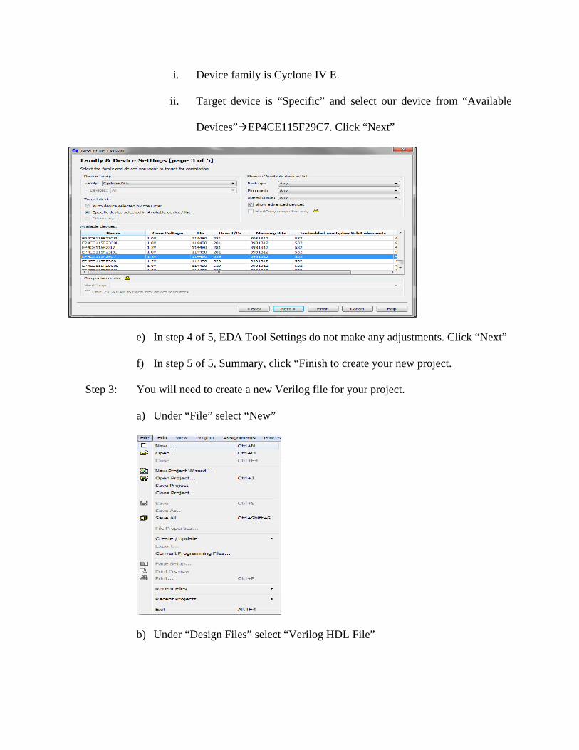
i. Device family is Cyclone IV E.
ii. Target device is “Specific” and select our device from “Available
Devices”EP4CE115F29C7. Click “Next”
e) In step 4 of 5, EDA Tool Settings do not make any adjustments. Click “Next”
f) In step 5 of 5, Summary, click “Finish to create your new project.
Step 3: You will need to create a new Verilog file for your project.
a) Under “File” select “New”
b) Under “Design Files” select “Verilog HDL File”
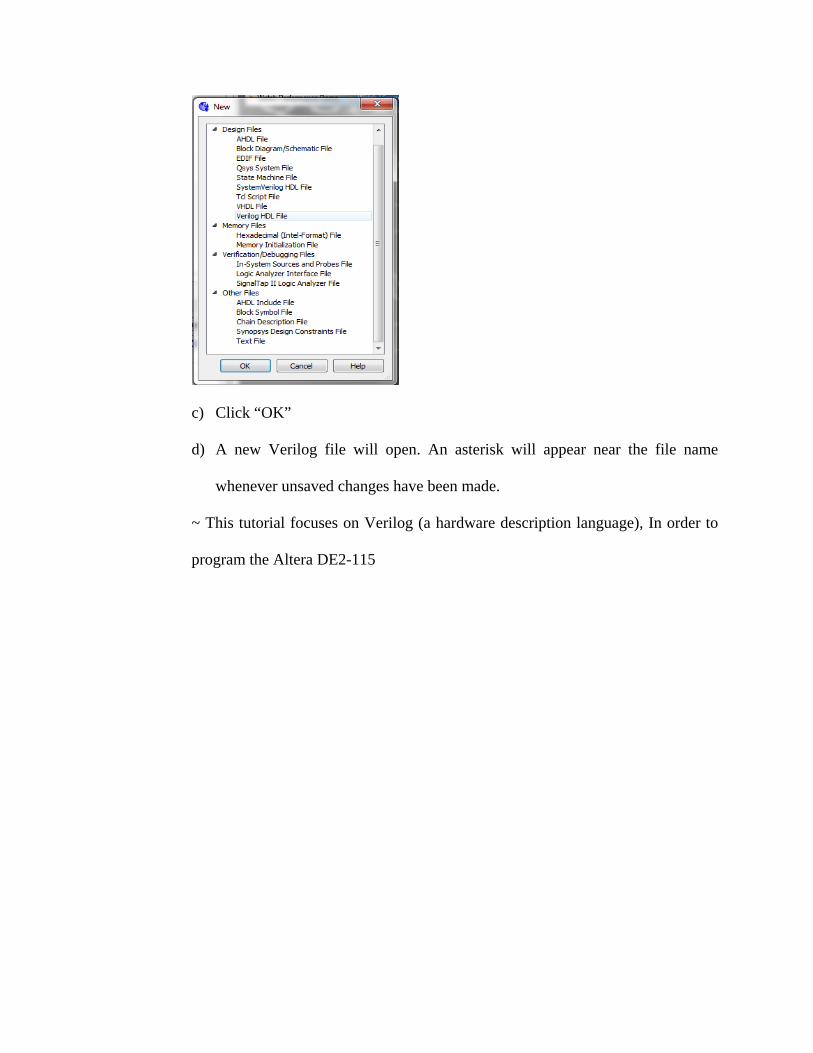
c) Click “OK”
d) A new Verilog file will open. An asterisk will appear near the file name
whenever unsaved changes have been made.
~ This tutorial focuses on Verilog (a hardware description language), In order to
program the Altera DE2-115
Step 4: Copy the Verilog Code from the file Binary_Adder.txt file into Quartus II
Note: Binary_Adder.txt is located in the Codes folder
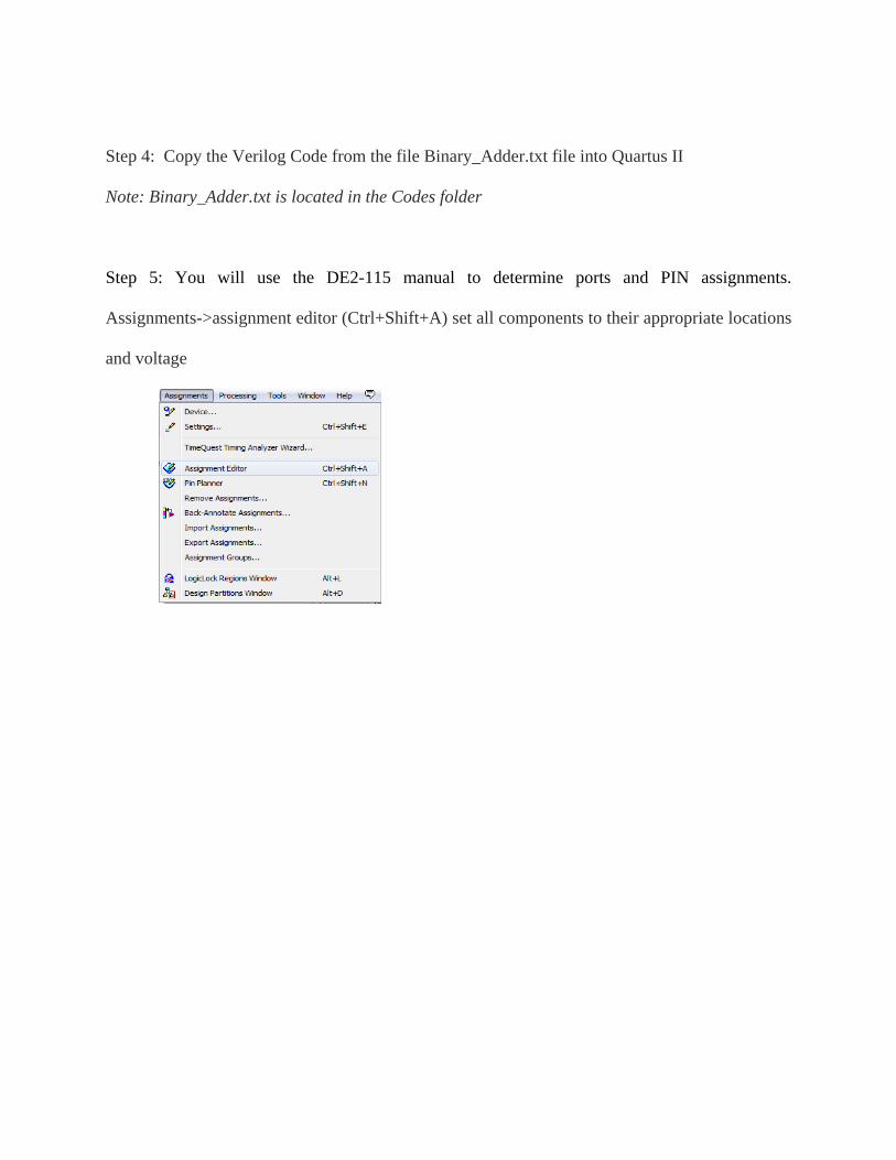
Step 5: You will use the DE2-115 manual to determine ports and PIN assignments.
Assignments->assignment editor (Ctrl+Shift+A) set all components to their appropriate locations
and voltage

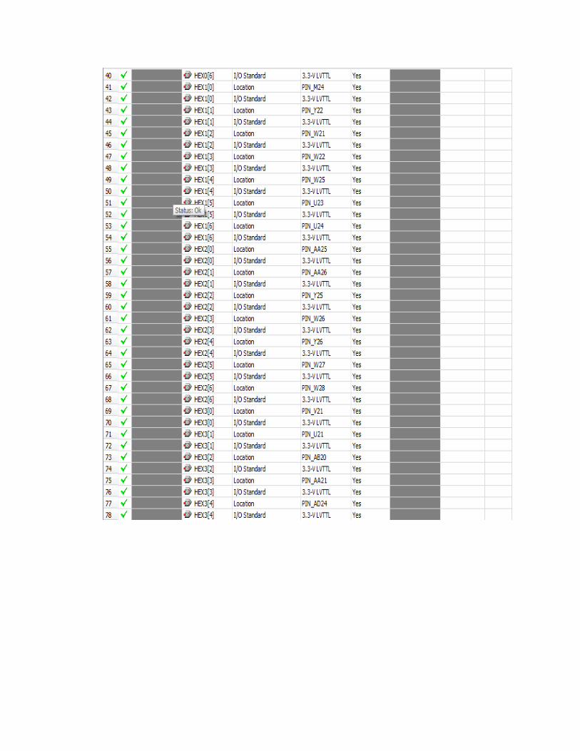
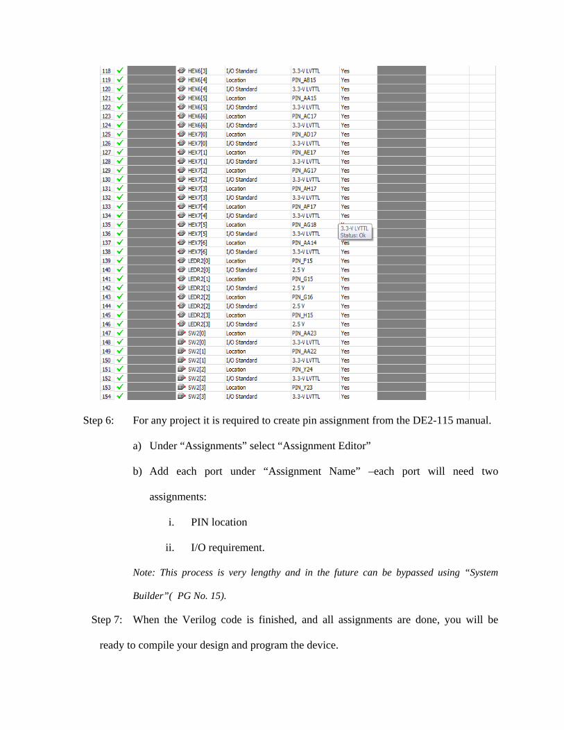
Step 6: For any project it is required to create pin assignment from the DE2-115 manual.
a) Under “Assignments” select “Assignment Editor”
b) Add each port under “Assignment Name” –each port will need two
assignments:
i. PIN location
ii. I/O requirement.
Note: This process is very lengthy and in the future can be bypassed using “System
Builder”( PG No. 15).
Step 7: When the Verilog code is finished, and all assignments are done, you will be
ready to compile your design and program the device.
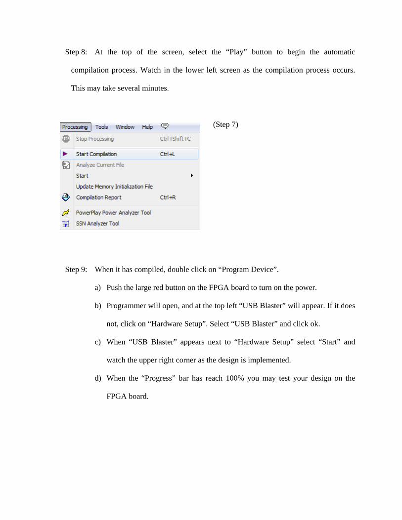
Step 8: At the top of the screen, select the “Play” button to begin the automatic
compilation process. Watch in the lower left screen as the compilation process occurs.
This may take several minutes.
(Step 7)
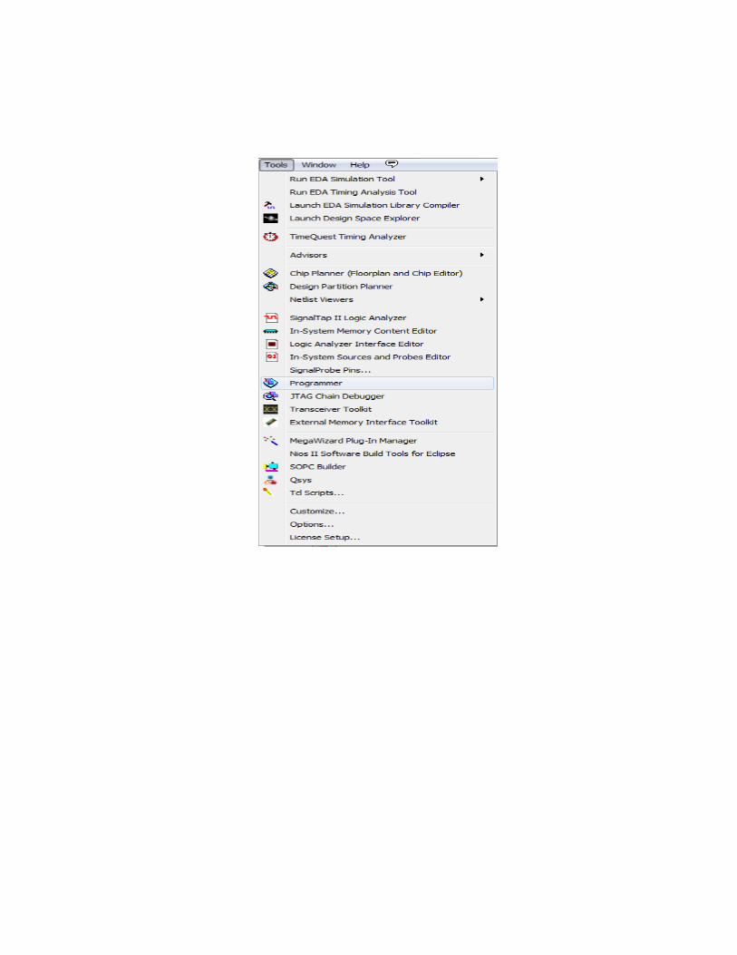
Step 9: When it has compiled, double click on “Program Device”.
a) Push the large red button on the FPGA board to turn on the power.
b) Programmer will open, and at the top left “USB Blaster” will appear. If it does
not, click on “Hardware Setup”. Select “USB Blaster” and click ok.
c) When “USB Blaster” appears next to “Hardware Setup” select “Start” and
watch the upper right corner as the design is implemented.
d) When the “Progress” bar has reach 100% you may test your design on the
FPGA board.
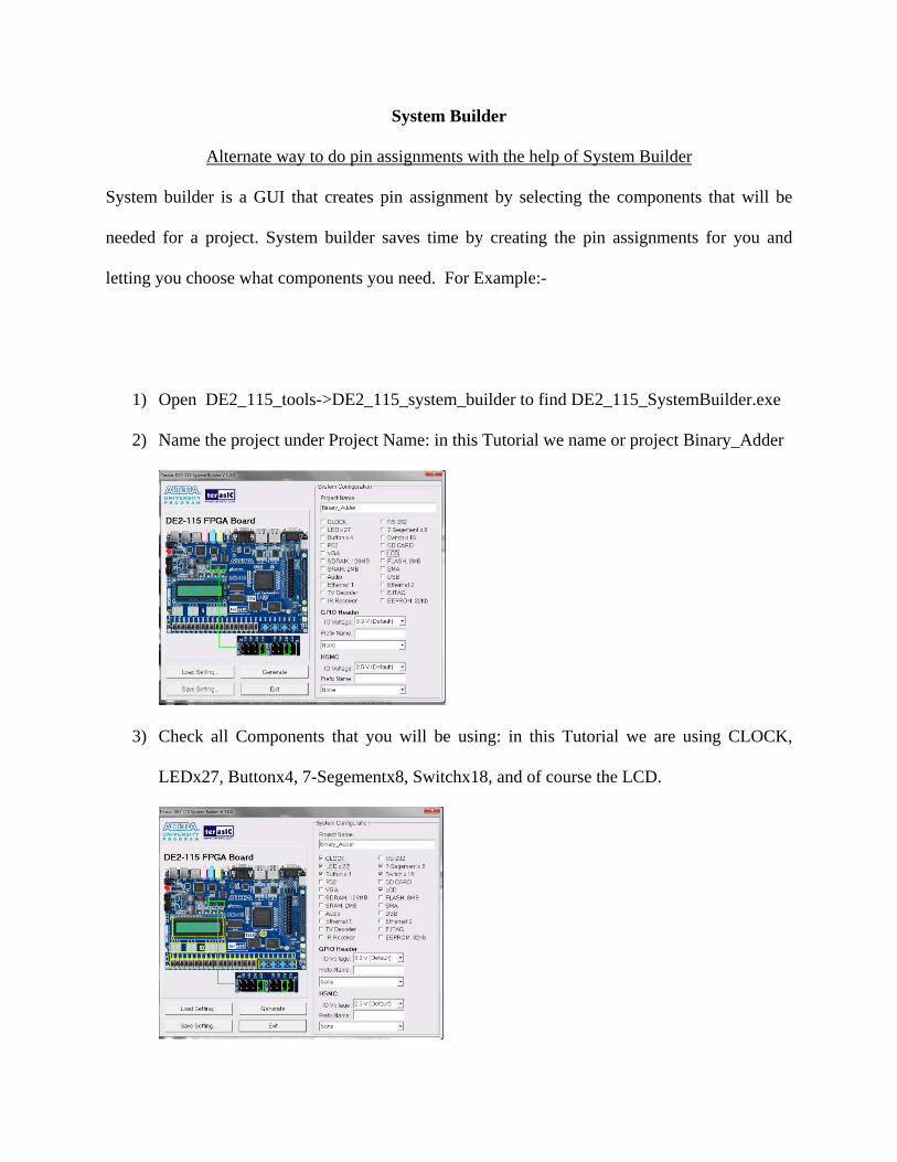
System Builder
Alternate way to do pin assignments with the help of System Builder
System builder is a GUI that creates pin assignment by selecting the components that will be
needed for a project. System builder saves time by creating the pin assignments for you and
letting you choose what components you need. For Example:-
1) Open DE2_115_tools->DE2_115_system_builder to find DE2_115_SystemBuilder.exe
2) Name the project under Project Name: in this Tutorial we name or project Binary_Adder
3) Check all Components that you will be using: in this Tutorial we are using CLOCK,
LEDx27, Buttonx4, 7-Segementx8, Switchx18, and of course the LCD.
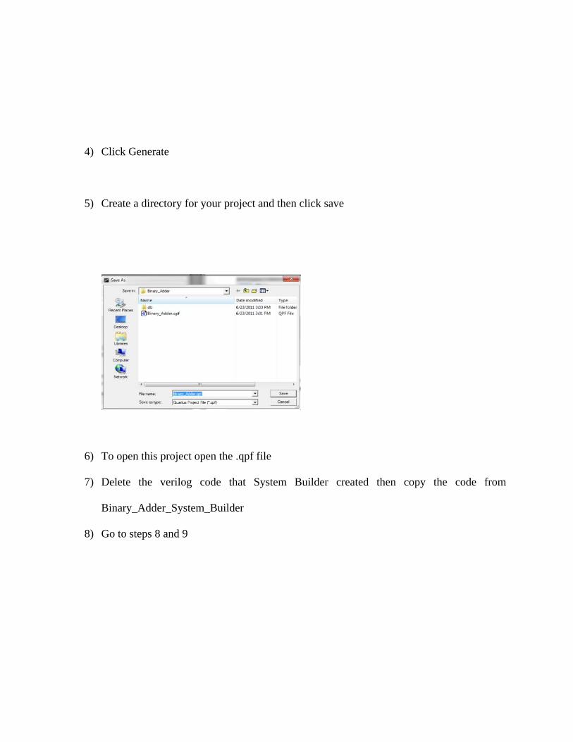
4) Click Generate
5) Create a directory for your project and then click save
6) To open this project open the .qpf file
7) Delete the verilog code that System Builder created then copy the code from
Binary_Adder_System_Builder
8) Go to steps 8 and 9
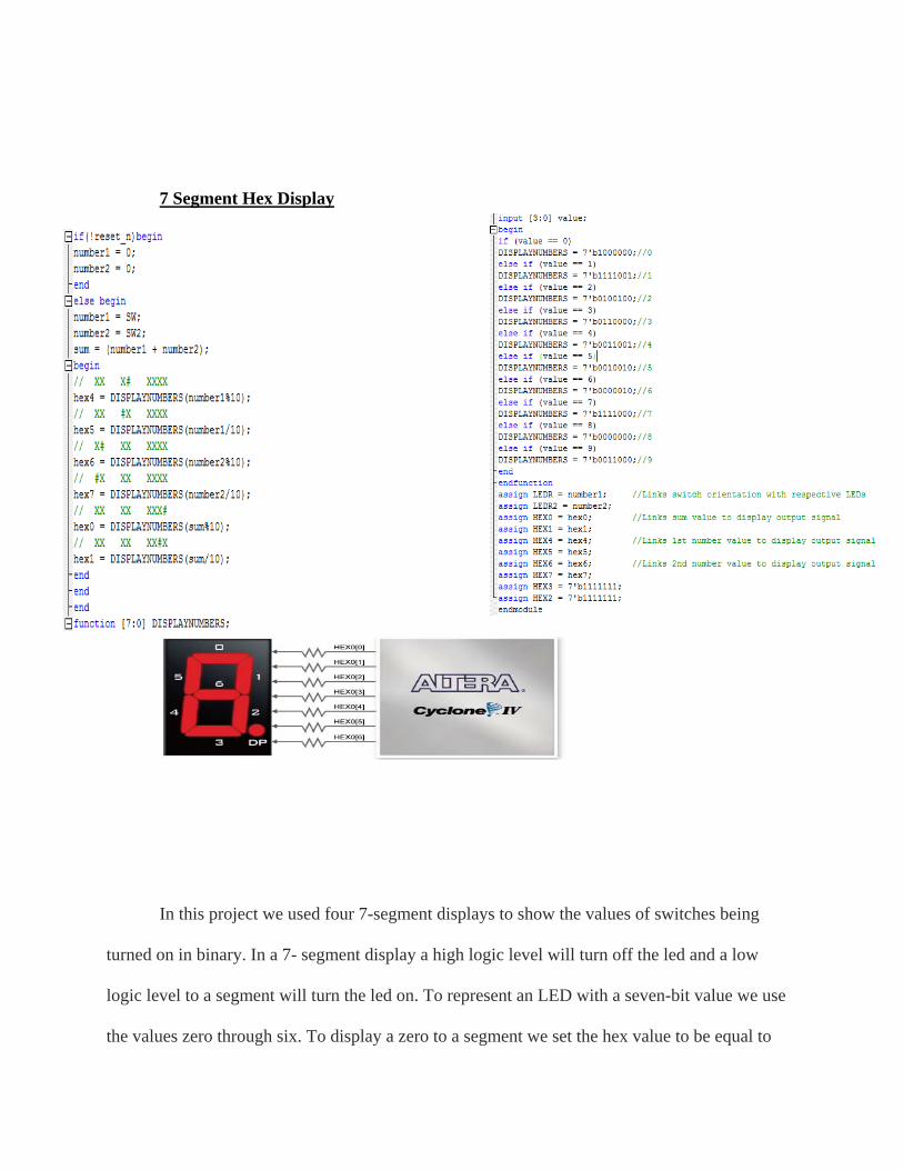
7 Segment Hex Display
In this project we used four 7-segment displays to show the values of switches being
turned on in binary. In a 7- segment display a high logic level will turn off the led and a low
logic level to a segment will turn the led on. To represent an LED with a seven-bit value we use
the values zero through six. To display a zero to a segment we set the hex value to be equal to

7b’1000000. This is because a zero will have all led on but the center led (number 6 on the figure
above). The code also uses a function to simplify the task of representing a bit value to a hex
value. Since the function DISPLAYNUMBERS only has one output it seemed like a function
instead of a task. In the function we have only one input value that represents a 4 bit switch
value, this value is passed through a series of if else statements to determine the hex value. At the
end of this program we assign all appropriate values to the represented LEDs.
There is a quick example of getting the LED’s, Switches, Keys, and 7 segment Hex
Display to function properly in the link below that goes more in detail about the 7 segment
display.
http://www.youtube.com/user/montoya332?blend=6&ob=5#p/a/u/0/78JQ4IgF9yc
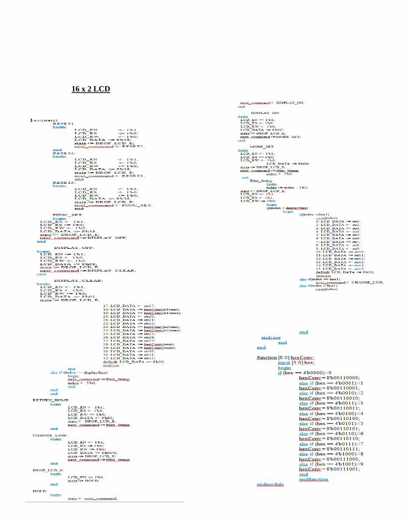
16 x 2 LCD
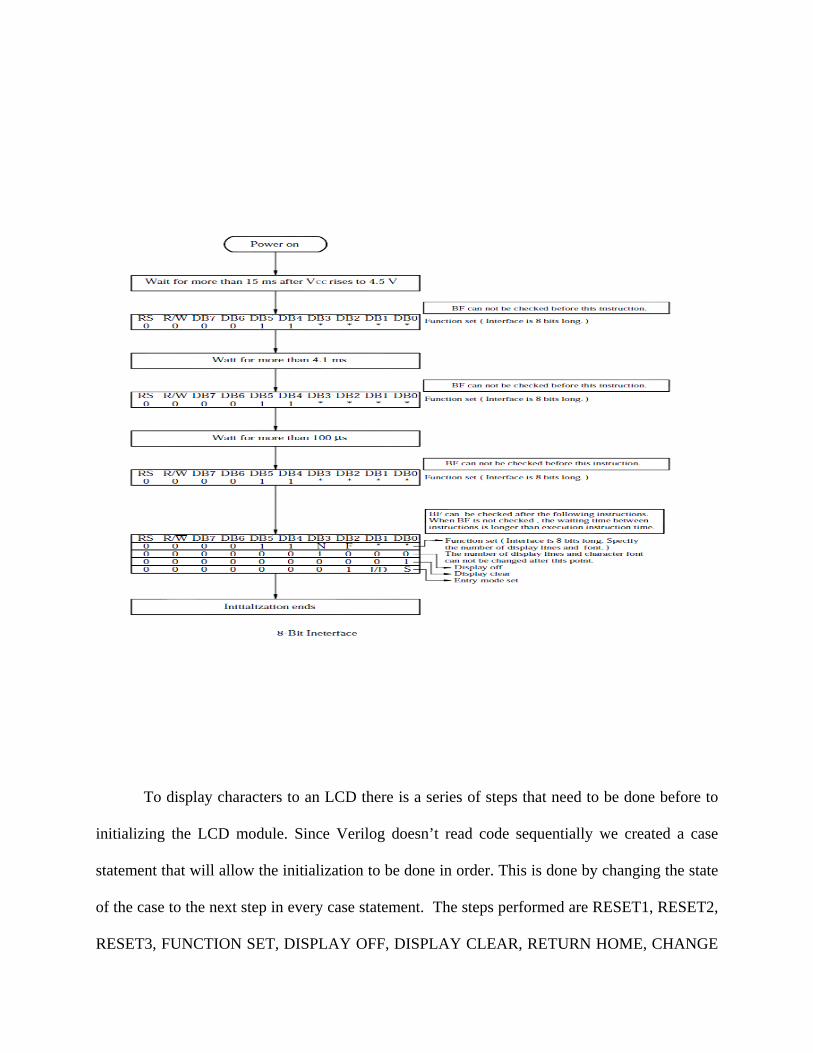
To display characters to an LCD there is a series of steps that need to be done before to
initializing the LCD module. Since Verilog doesn’t read code sequentially we created a case
statement that will allow the initialization to be done in order. This is done by changing the state
of the case to the next step in every case statement. The steps performed are RESET1, RESET2,
RESET3, FUNCTION SET, DISPLAY OFF, DISPLAY CLEAR, RETURN HOME, CHANGE

LINE, DROP LCD, HOLD, DISPLAY ON, and MODE SET AND PRINT STRING. These
reset needs to be done three time to because we need to initialize enable to high and register
select and read/write to low signals. These steps are also done to communicate with the LCD to
determine if it will be an 8 or 4 bit data bus, this is done by setting the data bus equal to the hex
value eight(8’h38). Before we can write to the screen we need to clear the LCD display, this is
done by changing the data bus equal to 8’h01 (Start of heading). Finally when we need to display
the screen we set enable and read/write to high and reset to low, this is done because this allows
us to write data to the LCD. In the print string case statement we added an else if (index ==line1)
because without this the LCD wouldn’t know when the next line begin or the first line starts.