Embed Size (px)
Citation preview

90
Chapter 5
Three Dimensional Surface Ribbon Method
When the dimension of the structure is electrically small, the signal paths can be
made short by sub-division and the quasi-static approach is sensible for the calcula-
tion of equivalent circuit models. For the simple case of non-parallel lines, as men-
tioned earlier, the volume filament method (VFM) is applicable with rather compli-
cated integration of Green's function as in [61]. Discontinuities such as a microstrip
line bend, via-hole, etc. have been examined using the integral equation method as-
suming perfect conductors and using scalar current potential or scalar magnetostatic
potential as state variables [68, 69]. For general structures frequency dependent resis-
tance and inductance can be obtained by solving the volume current integral equation
in three dimension, which is known as the partial element equivalent circuit method
(PEEC) [54, 60, 64, 70-73]. Full-wave techniques have also been applied to analyzing
three dimensional geometries, but at the expense of increased numerical burden. The
full-wave spectral domain method (SDM) has been used in analyzing a spiral inductor
having an air-bridge, with the assumption of perfect conductors [74]. The electric
field integral equation (EFIE) using the standard impedance boundary condition
(SIBC) has also been developed for characterizing three dimensional structures of mi-
crostrip line, via, and meshed reference plane at high frequency [9, 10, 54, 75]. The
finite difference time domain method (FDTD) has been used to characterizing discon-
tinuities and reference planes [76-79].
In the previous chapter, the effective internal impedance (EII) was successfully
combined with the current integral equation and it significantly reduced computation

91
time. This approach can be extended into three dimensional geometries under the
quasi-static assumption [80]. In this chapter, EII will be defined for all ribbons on the
surfaces of the conductor according to the direction of current flows, the surface cur-
rent integral equations will be derived, and the current continuity condition will be
applied. This three dimensional surface ribbon method (3DSRM) can be utilized
where PEEC can calculate frequency dependent resistance and inductance, such as the
discontinuities of bend and simple via, various reference planes, meander lines, etc.
The efficiency and accuracy of this 3DSRM will be examined through examples of
right-angled bends, meander lines, and a microstrip line with a meshed ground plane.
For comparison PEEC will be applied and the volume filament method (VFM) will be
used with a two dimensional approximation.
5.1 Partial Element Equivalent Circuit Technique
Ruehli [70] developed the partial element equivalent circuit method (PEEC) for
evaluating capacitance and frequency dependent resistance and inductance of three
dimensional geometries. And recently he has proved that the full-wave form of
PEEC is no more than exploiting the method of moments [81, 82]. He also derived a
quasi-static form of PEEC and applied it to evaluating resistance and inductance of a
microstrip line bend [71] and ground plane connections [60]. This approach is based
on the volume current integral equation using current vector as state variables, shown
in (4.6). Current continuity condition is enforced by applying Kirchhoff's current law
or voltage law, and, therefore, a nodal-based or mesh-based matrix is formed to be
solved. Also hybrid finite element method and method of moments was developed to
solve this volume integral equation in two steps instead of nodal-based or mesh-based

92
approach, and has been utilized to solve a microstrip bend and simple shaped vias
[83].
Recently, PEEC has been applied to calculating the frequency dependent induc-
tance of a ceramic quad flat pack (CQFP) having about 200 pins, considering the skin
effect of the non-straight signal paths and frequency dependent current distribution on
a ground plane [84]. And it has been utilized to calculate the inductance of a via [85]
and can also be applied to the effective inductance evaluation of reference planes pre-
sented in [86, 87] for the evaluation of simultaneous switching noise. But PEEC
needs an increasing number of segments to appropriately account for frequency de-
pendent resistance and inductance due to the skin and proximity effects at high fre-
quency and for complicated structures. To reduce the numerical complexity thick
conductors can be replaced by a thin strip and sheet resistance as in [84], which is
applicable for limited structures and does not accurately capture the high frequency
resistance.
Instead of approximating the structure a preconditioned generalized minimal
residual (GMRES) algorithm or a conjugate gradient algorithm can be adopted as a
fast iterative matrix solver, instead of expensive direct matrix solvers such as gaussian
elimination or LU decomposition. The speed of this approach can be enhanced with
the use of a multipole-accelerated algorithm for fast and approximated matrix-vector
multiplication [64]. Also PEEC has been speeded up more by a FFT-based algorithm
for matrix-vector multiplication in case of an uniformly segmented arbitrarily shaped
reference plane [72, 73]. To capture the finite conductivity and the skin and proxim-
ity effects fine discretization is required and it could be avoided by extending the

93
SRM into three dimensional geometries. In addition, numerically efficient techniques
can be incorporated with SRM as well as PEEC.
5.2 Three Dimensional Surface Ribbon Method
Instead of solving the volume current integral equation inside of the conductor in
PEEC, only the surface of the conductor is segmented into ribbons and at each ribbon
and along the current flow direction EII is defined to represent the characteristics of
the conductor interior, as in two dimensional problem. Unlike the two dimensional
problem where the current continuity condition is inherently satisfied, this condition
should be enforced in the surface current integral equations as in PEEC. In following
sub-sections, the segmentation scheme of 3DSRM will be explained compared to
PEEC, the EII will be defined using the transmission line model, and mesh-based
analysis will be considered.
5.2.1 Discretization and Effective Internal Impedance
In PEEC, the conductor is divided into small hexahedrons as shown in the right-
angled bend structure of Fig. 5.1(a), a node is placed at the center of each hexahedron,
and a partial element is defined between two adjoining nodes, as shown in Fig. 5.1(b).
The volume current integral equation is expanded and tested at each element using
pulse basis functions and, therefore, three dimensional current flow is considered in-
side of the conductor. In 3DSRM, the conductor surface is divided into rectangular
patches as in Fig. 5.2(a), a node is also given at the center of each rectangular patch,
and a ribbon is defined between two adjoining nodes as in Fig. 5.2(b). Therefore, the
number of segments is reduced by replacing volume discretization of the order N3 in
PEEC by surface discretization of the order N2 in 3DSRM.

94
JJ
unit cell junit cell i
element (i,j)
node j
node i
(a) (b)
Figure 5.1: Discretization of the conductor inside for the use of partial element
equivalent circuits (PEEC) method in an example of a right-angled bend. (a) The
conductor is divided into small hexahedrons, and (b) an element is defined between
adjoining nodes placed at the center of the hexahedrons; arrow indicates direction of
current flow.
unit cell junit cell i
Jnode j
J
node i
ribbon (i,j)
(a) (b)
Figure 5.2: Discretization of the conductor surface for the use of the three-dimen-
sional surface ribbon method (3DSRM) in an example of a right-angled bend. (a) The
conductor surface is divided into small rectangular patches, and (b) a ribbon is de-
fined between adjoining nodes placed at the center of the rectangles; arrow indicates
direction of current flow.

95
x y
z x y
z
(a) (b)
x y
z
(c)
Figure 5.3: Sub-divisions of the conductor interior for defining the effective internal
impedance (EII) along the direction of current flows in an example of a right-angled
bend. (a) y-axis, (b) z-axis, (c) x-axis; arrows indicate direction of current flow.
Based on the above discretization scheme, two directional surface current is de-
fined all over the surface of the conductor. And on each ribbon EII should be as-
signed the appropriate modeling corresponding to the direction of the surface current.
One possible way to define EII on three dimensional geometries is to approximate the
surface impedance of the structure, but it is hard to guess the surface impedance be-

96
cause of the complicated geometries. As in reference [20] and Chapter Two the plane
wave model could be modified or extended to account for arbitrary three dimensional
geometries. Or the transmission line model in Chapter Two could be extended into
three dimensional geometries. In this study, the transmission line model is easily ex-
tended into three dimensional structures. Figure 5.3 shows how to divide the conduc-
tor interior for EII models along all directions of the current for an example of a right-
angled bend. At and near the corner two tangential currents are defined and for uni-
form sections only longitudinal current is assumed. Where the number of outer sur-
faces are four, EII is defined as in two dimensional problems. If the number of outer
surfaces are three, then the rectangular cross-section is divided into two pairs of
isosceles triangles near two corners of adjoining surfaces and flat rectangles for what
remains. For adjoining two surfaces it is divided into two isosceles triangles at the
corner and two flat rectangles for what remains, and for two parallel surfaces it is di-
vided into two flat rectangles. For each isosceles triangle EII is derived using the
transmission line model, and for each rectangle the surface impedance of a flat con-
ductor is used as explained in Chapter Two.
5.2.2 Current Continuity Condition and Mesh Analysis
The surface current integral equation of (4.12) is driven at each ribbon. The
impedance matrix can be deduced by relating current and voltage at each ribbon as
follows
Z[ ] Ir[ ] = Vr[ ], (5.1)
where Vr[ ] and Ir[ ] are n ×1 ribbon voltage and current vectors, n is the number of
ribbons, and n × n impedance matrix of Z[ ] is given by

97
Z[ ] = Zeii (ω )[ ] + jω L[ ] (5.2)
To ensure the current continuity condition, Kirchhoff's voltage law (KVL) is applied
to the matrix equation of (5.1) that then leads to mesh analysis, which has fewer un-
knowns and a more regular matrix than the nodal analysis using Kirchhoff's current
law (KCL). KVL is expressed using the mesh matrix relating each ribbon and meshes
by
M[ ] Vr[ ] = Vm[ ] (5.3)
where M[ ] is the m × n mesh matrix, Vm[ ] is the m ×1 mesh voltage vector, and m
is the number of meshes. The mesh voltages are almost zero except the meshes where
external sources are applied. Also current on each ribbon is related to mesh currents
using the above mesh matrix as follows
M[ ]t Im[ ] = Ir[ ], (5.4)
Figure 5.4: Circuital representation of the three-dimensional surface ribbon method
(3DSRM) in case of a right-angled bend.

98
where Im[ ] is the m ×1 mesh current vector. Finally, the mesh matrix equation is
formed by
M[ ] Z[ ] M[ ]t Im[ ] = Vm[ ] (5.5)
The above procedure is identical to the mesh analysis [64] in PEEC, and fre-
quency dependent resistance and inductance are obtained by solving the above matrix
with direct or iterative matrix solvers. Figure 5.4 shows the equivalent circuits of the
mesh analysis for an example of a right-angled bend.
5.3 Examples
The accuracy and efficiency of 3DSRM could be shown by characterizing dis-
continuities and complex planar structures of high frequency circuits. Because the
quasi-static approximation is valid not only for uniform lines but also for discontinu-
ities such as bends and vias, a lumped circuit model can be used to represent the dis-
continuities. First, coupled right-angled bends are examined as one of the simplest
cases. When the planar structure becomes complicated and the non-uniform parts are
not negligible, the non-uniform structures can not be simplified into uniform lines.
The series impedance of coupled meander lines are analyzed as a complicated case.
And a microstrip line with a meshed ground plane is examined to see the effects of
mesh pitch and apertures. For comparisons PEEC is used and the volume filament
method (VFM) is also applied, but this requires simplifying the geometries.
5.3.1 Coupled Right-angled Bends
Figure 5.5 shows coupled right-angled bends, where the rectangular conductors
are 10 µm wide and 10 µm thick, placed on a plane with gap of 10 µm, and conduc-

99
tivity 5.8 ×10⁷ [S/m]. For that structure resistance and inductance are calculated by
3DSRM, PEEC, and approximated using VFM, To distinguish bend discontinuities
from uniform lines two reference planes are placed from the corner of outer lines at a
distance ld = 35 µm. These planes are selected where the current distribution is
within 10% that of uniform lines VFM simplifies the structure into two pairs of
straight lines with length chosen to give correct DC resistance. The "excess" resis-
tance and inductance of the bends are obtained by subtracting the impedance of uni-
form lines from the total impedance as follows
Rdis = Rtot − Runi
Ldis = Ltot − Luni(5.6)
where Rtot and Ltot are the total resistance and inductance, and Runi and Luni are the
resistance and inductance of two pairs of twin uniform lines with the length of l − ld .
Resistance and inductance of uniform lines are calculated with VFM for PEEC and
l
t = 10
µm
g = 10 µm
w = 10 µm
ld = 35 µm
y z
x
Figure 5.5: Coupled right-angled bends. The lines are 10 µm wide, 10 µm thick, 10
µm spacing, and conductivity 5.8 ×10⁷ [S/m]. Discontinuity section is defined on the
bends from the corner of outer lines with ld = 35 µm.

100
0.01
0.10.12
20
22
24
26
28
0.01 0.1 1 10 30Frequency [GHz]
Res
ista
nce
Rdi
s [Ω
]
Indu
ctan
ce L
dis [
pH]A
B
C
(a)
0.85
0.9
0.95
1
1.05
20 100 1000
Nor
mal
ized
Res
ista
nce
at 1
0 G
Hz
l - ld [µm]
B
C
0.98
1
1.02
1.04
20 100 1000
Nor
mal
ized
Ind
ucta
nce
at 1
0 G
Hz
l - ld [µm]
B C
(b) (c)
Figure 5.6: Comparison of resistance and inductance of coupled right-angled bends
between partial element equivalent circuits method (PEEC), three-dimensional sur-
face ribbon method (3DSRM), and two-dimensional approximation using the volumefilament method (VFM). (a) Discontinuity resistance and inductance with l − ld =
100 µm, (b) Total resistance normalized by resistance, (c) Total inductance normal-
ized by inductance of uniform lines having the same DC resistance. A(8): PEEC;
B(solid line): 3DSRM; C(dotted line): 2-D approximation using VFM.

101
VFM, and two dimensional SRM for 3DSRM with the same segmentation scheme.
PEEC uses uniform 4 × 4 segments at each side of the conductor and 9 segments lon-
gitudinally, VFM uses uniform 10 × 10 segments, and 3DSRM uses uniform 3 seg-
ments at each surface of the conductor. This leads 973, 249, and 199 unknowns for
PEEC, 3DSRM, and VFM, respectively. Figure 5.6(a) shows resistance and induc-
tance and compares with each technique used, when the length l − ld is 100 µm. For
discontinuity inductance 3DSRM is close to PEEC with a deviation of less than 2%,
and VFM is off 6% at low frequency and agrees well at high frequencies. For discon-
tinuity resistance PEEC does not capture the skin effect fully at high frequency due to
coarse segments, and VFM give quite close answer to 3DSRM with 20% error.
For this simple bend having small non-uniform parts compared to uniform parts,
the discontinuities do not have significant effect under the quasi-static assumption.
To see the effect of bends, total resistance and inductance are normalized, respec-
tively, by resistance and inductance of twin uniform lines having the same DC resis-
tance as that of the original lines. Impedance of twin uniform lines is calculated by
SRM with 7 segments on each side of the conductor. Figure 5.6(b) compares normal-
ized resistance and Fig. 5.6(c) shows normalized inductance at the high frequency of
10 GHz. As shown in the figures, discontinuity resistance and inductance can be
simply approximated by straight lines having the same DC resistance for a line length
longer than 100 µm.
5.3.2. Coupled Meander Lines
Like the rectangular spiral inductor in reference [74], the corners of meander
lines with short uniform sections may have significant effect on frequency dependent
resistance and inductance. When the meandering is periodically repeated, one period

102
is named the unit cell; two periods of coupled meander lines are drawn in Fig. 5.7.
The rectangular conductor is 10 µm wide and 10 µm thick, the pitch of a period is 40
µm, two lines are spaced with gap of 10 µm, and the conductivity is 5.8 ×10⁷ [S/m].
Because of the periodicity of the structure the periodic condition can be enforced into
the current integral equations, and again the number of unknowns can be reduced by a
half due to mirror image symmetries. Thus, the number of unknowns can be kept to
that of unit cell regardless of the line length. The surfaces of lines is expressed by
unit cell geometries as follows
Sall x, y, z( ) = Suc (−1)i x,y,z+kP( )k=0
nc
∑i=0
1
∑ , (5.7)
where Sall is the surface of the entire lines, Suc is the surface of a unit cell, nc is the
number of periods, and P is the pitch of a period. Therefore, the matrix equation of
(4.13) can be rewritten as follows
Zeii r x, y, z( )( )[ ] + jω L r x, y, z( ), ′r (−1)i ′x , ′y , ′z + kP( )( )[ ]k=0
nc
∑i=0
1
∑
Ir[ ] = Vr[ ] (5.8)
where r x, y, z( ), ′r ′x , ′y , ′z( ) ∈Suc . The above periodic condition requires more time
for assembling the matrix as the line length increases, but the number of unknowns
remains the same and matrix solving time is constant.
Resistance and inductance of meander lines with 10 cells has been calculated us-
ing 3DSRM, PEEC, and approximated using VFM. Figure 5.8(a) shows resistance
and inductance per period and compares the results with each other. Like in the case
of right-angled bends VFM uses the simplified structure of cascaded straight lines
giving correct DC resistance. PEEC uses uniform 5 × 4 segments at each side of the

103
. .
P= 40 µm
d = 10 µm
g = 10 µm
t = 10
µmw
= 1
0 µ
m
y z
x
Figure 5.7: Coupled meander lines. The lines are 10 µm wide, 10 µm thick, 10 µm
spacing, 40 µm period, and conductivity 5.8 ×10⁷ [S/m]. Two lines are mirror sym-
metric against yz -plane with x=0.
conductor, VFM uses uniform 10 × 10 segments, and 3DSRM uses uniform 3 seg-
ments at each surface of the conductor. This leads to 1021, 209, and 397 unknowns
for PEEC, 3DSRM, and VFM, respectively. For inductance 3DSRM is close to
PEEC with deviation of less than 3%, and VFM is considerably off 26% due to un-
derestimated line length. For resistance 3DSRM and PEEC are matched well up to
about 3 GHz, within 3%, and beyond that PEEC does not capture the skin effect fully
due to coarse segments, and VFM is off 30% from 3DSRM. Figure 5.8(b) compares
inductance vs. line length. When the line length becomes longer than 5 times the pe-
riod, per unit period inductance reaches a constant value. And 3DSRM and PEEC
give almost same low frequency inductance, are about 3% different for the high fre-
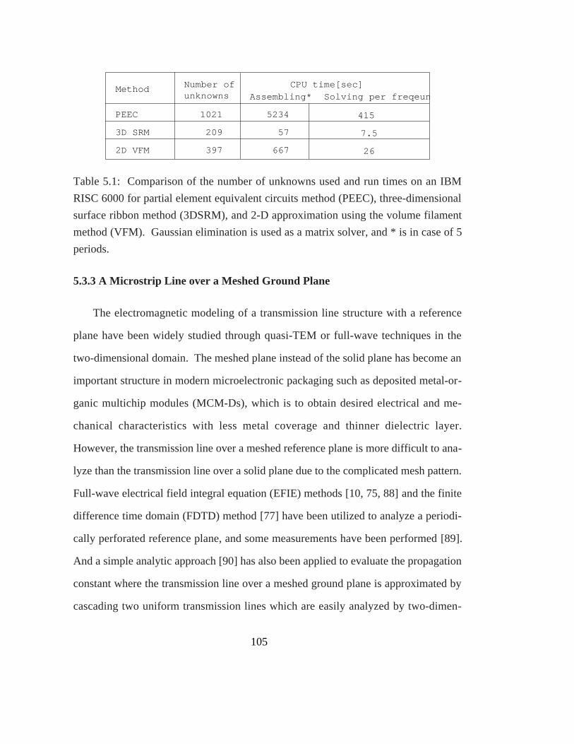
quency inductance, and VFM underestimates inductance about 26%. In Table 5.1 the
number of unknowns and the computation time are compared. It shows 3DSRM sig-
nificantly reduces the number of unknowns and CPU time over PEEC and even VFM
of two dimensional approximation.

104
0.01
0.1
0.2
20
25
30
35
40
0.01 0.1 1 10 30Frequency [GHz]
Res
ista
nce
Rce
ll [Ω
/cel
l]
Indu
ctan
ce L
cell [
pH/c
ell]
AB
C
(a)
15
20
25
30
35
40
1 2 3 4 5 6 7 8 9 10Number of Cell
AB
C
low frequency
high frequency
Indu
ctan
ce L
cell [
pH/c
ell]
(b)
Figure 5.8: Comparison of resistance and inductance of coupled meander lines be-
tween partial element equivalent circuits method (PEEC), three-dimensional surface
ribbon method (3DSRM), and two-dimensional approximation using the volume fil-
ament method (VFM). (a) Per unit period resistance and inductance calculated with
10 periods, (b) Per unit period inductance calculated vs. the number of periods. A(8):
PEEC; B(solid line): 3DSRM; C(dotted line): 2-D approximation using VFM.
105
Method Number ofunknowns
CPU time[sec]Assembling* Solving per freqeun
PEEC
3D SRM
2D VFM
1021
397
5234
57
667
415
7.5
26
209
Table 5.1: Comparison of the number of unknowns used and run times on an IBM
RISC 6000 for partial element equivalent circuits method (PEEC), three-dimensional
surface ribbon method (3DSRM), and 2-D approximation using the volume filament
method (VFM). Gaussian elimination is used as a matrix solver, and * is in case of 5
periods.
5.3.3 A Microstrip Line over a Meshed Ground Plane
The electromagnetic modeling of a transmission line structure with a reference
plane have been widely studied through quasi-TEM or full-wave techniques in the
two-dimensional domain. The meshed plane instead of the solid plane has become an
important structure in modern microelectronic packaging such as deposited metal-or-
ganic multichip modules (MCM-Ds), which is to obtain desired electrical and me-
chanical characteristics with less metal coverage and thinner dielectric layer.
However, the transmission line over a meshed reference plane is more difficult to ana-
lyze than the transmission line over a solid plane due to the complicated mesh pattern.
Full-wave electrical field integral equation (EFIE) methods [10, 75, 88] and the finite
difference time domain (FDTD) method [77] have been utilized to analyze a periodi-
cally perforated reference plane, and some measurements have been performed [89].
And a simple analytic approach [90] has also been applied to evaluate the propagation
constant where the transmission line over a meshed ground plane is approximated by
cascading two uniform transmission lines which are easily analyzed by two-dimen-

106
sional quasi-TEM field solvers. But the studies are mainly focused on calculating
high frequency characteristic impedance and propagation constant, frequency depen-
dent loss, so the effect of the reference plane have not been fully examined. In this
section, 3DSRM as well as PEEC is applied to calculate frequency dependent resis-
tance and inductance of the transmission line over a periodically perforated ground
plane.
wt
x
yz
gp
t
h
Figure 5.9: A microstrip line over a meshed ground plane where the aperture is
placed at an angle of 45o with respect to the signal line. The signal line is 12 µm
wide, 2.5 µm thick, 12 µm over the ground, the mesh pitch is 100 µm, the aperture is
50 µm square, and the conductivity is 5.8 ×10⁷ [S/m].
Figure 5.9 shows part of a microstrip line over an obliquely oriented meshed
ground plane, where the signal line is 12 µm wide, 2.5 µm thick and 12 µm over the
ground plane, the ground plane has the mesh pitch of 100 µm, an aperture of 50 µm
square, the signal line is 45o with respect to x -axis, and the conductivity is 5.8 ×10⁷
[S/m]. The shaded part is a unit ground cell with the period of 100 2 µm, so the pe-
riodic condition is utilized as in 5.3.2. Resistance and inductance of this structure
with 5 apertures perpendicular to the signal line and 9 apertures along the signal line

107
were calculated by PEEC and 3DSRM. Figure 5.10 shows resistance and inductance
per unit length and compares the results with each other and a microstrip line over a
solid ground. PEEC exploits three different segmentation schemes. First, the meshed
ground is approximated by connecting straight lines and 6 × 3 segments are used at
each side of the conductor with width ratios of 3 and 2.5, respectively. Second, one
unit cell of the meshed ground is segmented by uniform 9 × 9 segments on xy-plane
and one layer segment is used along the z -axis. Third, one unit cell of meshed
ground is segmented by uniform 9 × 9 segments on xy-plane and two layer segments
are used along the z -axis. The signal line is non-uniformly segmented into 12 × 4
5
10
25
4
6
8
10
12
14
0.01 0.1 1 10
Indu
ctan
ce [
nH/c
m]
Frequency [GHz]δ=t δ=t/3
B
A
E
D
C
Res
ista
nce
[Ω/c
m]
Figure 5.10: Comparison of resistance and inductance of a microstrip line over a
meshed ground plane between partial element equivalent circuits method (PEEC),
three-dimensional surface ribbon method (3DSRM), and a microstrip line over a solid
ground. A(dashed line): PEEC with straight line approximation; B(dotted line):
PEEC with one layer segment of the ground; C(8): PEEC with two layer segments of
the ground; D(solid line): 3DSRM, E(dot-and-dashed line): a microstrip line over a
solid ground. Meshed ground is considered by 5 apertures perpendicular to the signal
line and 9 apertures along the signal line.
108
Method Number ofunknowns
CPU time[sec]Assembling* Solving per freqeun
PEEC1
PEEC2
PEEC3
398
743
1360.1
1788.4
4745.1
18.6
8.0
146.7
283
3D SRM 148 37.2 3.1
Table 5.2: Comparison of the number of unknowns used and run times on an IBM
RISC 6000 for three segmentation schemes of partial element equivalent circuits
method (PEEC) and three-dimensional surface ribbon method (3DSRM). Gaussian
elimination algorithm is used as a matrix solver, and * is in case of 9 periods.
12
14
16
18
20
22
24
40 50 60 70 80 90 100
A
B
C
D
Res
ista
nce
[Ω /c
m]
at t=
2.5δ
Mesh pitch [µm]
7
8
9
10
11
12
40 50 60 70 80 90 100
Hig
h Fr
eque
ncy
Indu
ctan
ce [
nH/c
m]
Mesh pitch [µm]
A
B
C
D
(a) (b)
Figure 5.11: Comparison of resistance and inductance of a microstrip line over a
meshed ground plane with varying mesh pitch. (a) Resistance at t = 2.5δ vs. mesh
pitch, (b) High frequency inductance vs. mesh pitch. Aperture ratio = g / p( )2 × 100
[%]. A(O and solid line): 3DSRM at 50% aperture, B(O and dotted line): PEEC with
straight line approximation at 50% aperture, C(8 and solid line): 3DSRM at 25%
aperture, D(8 and dotted line): PEEC with straight line approximation at 25% aper-
ture.

109
segments on each side with width ratios of 1.4 and 2, respectively, for all three seg-
mentation schemes. These three segmentation schemes are identified as PEEC1,
PEEC2, and PEEC3, respectively. 3DSRM uses uniform 7 × 7 segments in the xy-
plane and three segments with width ratio of 2.8 for the wide surface and one segment
for the narrow surface of the signal line. To reduce the number of unknowns only the
top surface of the meshed ground is segmented instead of all surfaces. The strip
width of the meshed ground is approximately increased by the thickness to account
for the effect of finite thickness edges. This leads to 398, 283, 743 and 148 unknowns
for the three PEECs and 3DSRM, respectively. For inductance 3DSRM is close to
PEEC2 and PEEC3 with a deviation of 5% at low frequency and 4% at high fre-
quency, while PEEC1 is considerably off about 23% due to the simplified geometry
and overestimated line length. For resistance, 3DSRM and the PEECs are matched
well up to δ = t . PEEC3 is off about 20% from 3DSRM at 10 GHz because coarse
segments are used on the meshed ground plane and, therefore, current crowding is
underestimated. Table 5.2 compares the number of unknowns and the computation
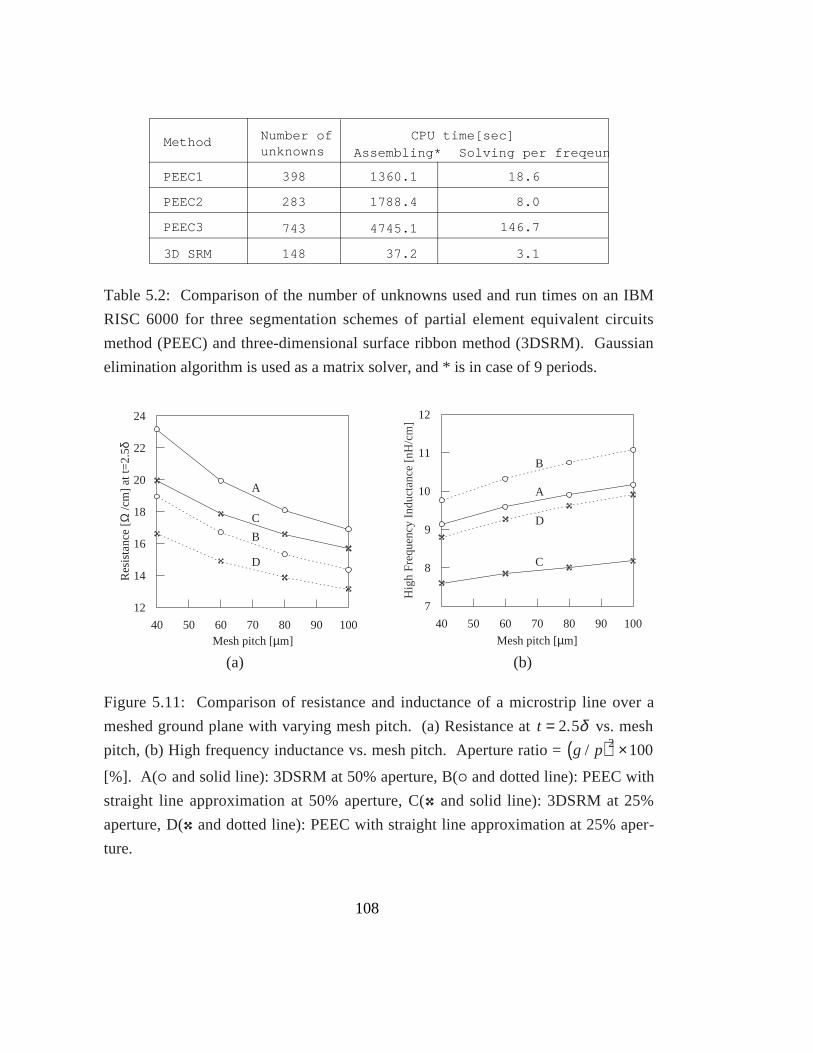
time of the various segmentation schemes and techniques used. When 3DSRM uses
uniform 12× 12 segments on one cell of the meshed ground plane, PEEC1 uses 6× 3
segments with width ratios of 3 and 2.5, respectively, on each side of simplified
straight lines, and 12 × 4 segments with width ratios of 1.4 and 2, respectively, on the
signal line for both cases. Figure 5.11 compares resistance and inductance vs. mesh
pitch. Figure 5.11(a) compares resistance at t = 2.5δ vs. mesh pitch, where PEEC1 is
off about 16% from 3DSRM. Figure 5.11(b) compares high frequency inductance vs.
mesh pitch, where for 25% aperture PEEC1 overestimated inductance about 20%
compared to the 3DSRM and for 50% aperture PEEC1 gives a slightly higher value
of 8% compared to 3DSRM. This indicates that the aperture ratio is becomes large

110
the simple approximation of straight lines is enough to capture the effect of the
meshed ground plane, as expected. Through this example the efficiency and accuracy
of 3DSRM is demonstrated by comparing the results to those of the more rigorous
PEEC.
5.4 Discussion and Further Considerations
Simple EII models have been derived for three dimensional geometries by ex-
tending the transmission line model from the two dimensional problems. EII can be
combined with the surface integral equations and the current continuity condition is
satisfied by applying Kirchhoff's voltage law (KVL). This 3DSRM is utilized to ex-
amine three examples and the accuracy and efficiency is verified.
Even though non-equal segments are used in this study, a more optimized non-
uniform discretization scheme can be developed to further enhance the efficiency of
the technique. This technique has been applied to structures having rectangular cross-
sections with rectangular segments, and it can be extended to the geometries of trape-
zoidal or circular cross-sections with developing the proper EII models. But to afford
a complicated geometries like a via-hole structure [74] triangular segments can be
used as in the full-wave electric field integral equation method (EFIE) of reference
[10, 54]. It may require higher order of basis functions [54] than pulse basis functions
and more CPU time to calculate the integral of Green's functions. The fast iterative
matrix solver [64] and FFT-based [72, 73] or multipole-accelerated matrix-vector
multiplication [64] can also be utilized in 3DSRM to enhance the numerical effi-
ciency.