Embed Size (px)
Citation preview

Chapter 6 – Selected Design TopicsPart 1 – The Design Space
Logic and Computer Design Fundamentals

Overview
Part 1 – The Design Space• Integrated Circuits
Levels of Integration
• CMOS Circuit Technology CMOS Transistor Models Circuits of Switches Fully Complementary CMOS Circuits Technology Parameters
Part 2 – Propagation Delay and Timing Part 3 – Asynchronous Interactions Part 4 - Programmable Implementation
Technologies

Integrated Circuits
Integrated circuit (informally, a “chip”) is a semiconductor crystal (most often silicon) containing the electronic components for the digital gates and storage elements which are interconnected on the chip.
Terminology - Levels of chip integration• SSI (small-scale integrated) - fewer than 10 gates
• MSI (medium-scale integrated) - 10 to 100 gates
• LSI (large-scale integrated) - 100 to thousands of gates
• VLSI (very large-scale integrated) - thousands to 100s of millions of gates

MOS Transistor
S (Source) D (Drain)G (Gate)
Substrate
Channellength Location of
conductinglayer
DD
n-ChannelTransistor: OFF - no D-to-S Currentr
0Volts V Volts0Volts

MOS Transistor
S (Source) D (Drain)G (Gate)
Substrate
Channellength Location of
conductinglayer
n-ChannelTransistor: ON - D-to-S Current
0Volts VDD VoltsVDD Volts

Switch Models for MOS Transistors
n-Channel – Normally Open (NO) Switch Contact
p-Channel – Normally Closed (NC) Switch Contact
XG
D
S
Symbol
X:••
Switch Model:
X:X
SimplifedSwitch Model
XG
D
S
•
Symbol
X:••
Switch Model
X:X
SimplifiedSwitch Model

Circuits of Switch Models
Series
Parallel
X: X
Y:Y
Series
X A ND Y
X: X Y:Y
Parallel
X OR Y

Fully-Complementary CMOS Circuit
Circuit structure for fully-complementary CMOS gate
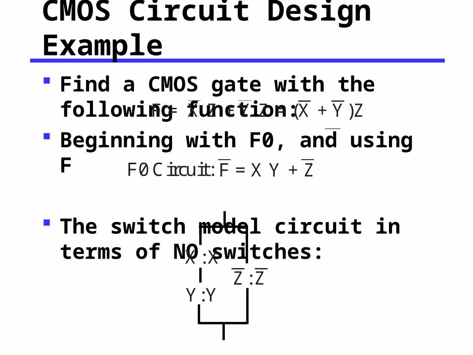
CMOS Circuit Design Example
Find a CMOS gate with the following function:
Beginning with F0, and using F
The switch model circuit in terms of NO switches:
F = X Z +Y Z = (X +Y )Z
F0 Circuit: F = X Y + Z
X: XZ: Z
Y:Y

CMOS Circuit Design Example
The switch model circuit for F1 in terms of NC contacts is the dual of the switch model circuit for F0:
The function for this circuit is:
which is the correct F.
X: X Y:Y
Z: Z
F = (X +Y ) ZF1 Circuit:

CMOS Circuit Design Example
Replacing theswitch modelswith CMOStransistors;note inputZ must be used.
•
+V
X
Z
From F1
From F0
••
•
•
•
•
Y
•
•
•
•

Technology Parameters
Specific gate implementation technologies are characterized by the following parameters: • Fan-in – the number of inputs available on a gate• Fan-out – the number of standard loads driven by a gate output• Logic Levels – the signal value ranges for 1 and 0 on the inputs
and 1 and 0 on the outputs (see Figure 1-1)• Noise Margin – the maximum external noise voltage superimposed
on a normal input value that will not cause an undesirable change in the circuit output
• Cost for a gate - a measure of the contribution by the gate to the cost of the integrated circuit
• Propagation Delay – The time required for a change in the value of a signal to propagate from an input to an output
• Power Dissipation – the amount of power drawn from the power supply and consumed by the gate

Fan-in
For high-speed circuits, fan-in is often restricted on gate primitives to no more than 4 or 5.
Fig. 6-4 Implementation of a 7-input NAND Gate

Fan-out
Fan-out can be defined in terms of a standard load• Example: 1 standard load equals the load
contributed by the input of 1 inverter.
• Transition time -the time required for the gate output to change from H to L, tHL, or from L to H, tLH
increases when load on the output increases
• The maximum fan-out that can be driven by a gate is the number of standard loads the gate can drive without exceeding its specified maximum transition time

Cost
In an integrated circuit:• The cost of a gate is proportional to the chip area
occupied by the gate
• The gate area is roughly proportional to the number and size of the transistors and the amount of wiring connecting them
• Ignoring the wiring area, the gate area is roughly proportional to the gate input count
• So gate input count is a rough measure of gate cost
If the actual chip layout area occupied by the gate is known, it is a far more accurate measure

Supplement documents
IC digital logic families • RTL ( Resistor-transistor logic)• DTL ( Diode-transistor logic)• TTL ( Transistor -transistor logic)• ECL ( Emitter-coupled logic)• MOS(Metal-oxide semiconductor)• CMOS ( Complementary Metal-oxide
semiconductor)

Supplement documents
),min(IL
OL
IH
OH
I
I
I
IoutFan
Computing fan-out

Supplement documents
CCCCD
CCLCCHCC
VavgIavgP
IIavgI
)()(2
)(
?7400)(
?)(
3,1
TTL standardFor
ICinavgPTotal
avgP
mAImAI
D
D
CCLCCH
Power dissipation

Supplement documents
TTL families

Example