Embed Size (px)
Citation preview

MT5F43750 © Fuji Electric Co., Ltd. All rights reserved.
Chapter 7 Typical Troubles and Troubleshooting
7-1
1. Troubleshooting 7-2
2. IGBT Test Procedures 7-7
3. Typical Troubles and Troubleshooting 7-8
MT5F43750 © Fuji Electric Co., Ltd. All rights reserved. 7-2
1. Troubleshooting
This chapter describes typical troubles and how to deal with them.
Table.7-1 Device destruction mode and cause estimation
When abnormalities such as device failure occurs, it is necessary to clarify the situation and determine the cause
before taking countermeasures. Referring to Table 7-1, please investigate the failure mode and analyze the
causes of abnormalities by observing the irregularities outside of the device. If the cause cannot be determined
by using Table 7-1, use the detailed diagram shown in Fig.7-1(a-f) to help your investigation.
External abnormalities Cause Device failure mode Check point
Short
circuit
Arm short
circuit
After short circuit detection, when protection is applied (turn-off), the overvoltage exceeds
SCSOA and the device is destroyed
SCSOA failure
(overvoltage)
destruction
Matching of the operation locus and
device withstand capability during
arm short circuit
Series arm
short circuit
(upper and
lower arm
short
circuit)
Insufficient dead timetoff increased due to insufficient -VGE, dead
time setting error
Overheat (short
circuit withstand
capability) failure
Check that toff and dead time match
dv/dt shoot through and causes short circuit
failureInsufficient -VGE, long gate wiring
SCSOA and
overheat failure
Check for dv/dt erroneous turn-on
Short circuit failure due to noise etc.Gate drive circuit malfunction, logic circuit
malfunctionCircuit malfunction check
Output
short circuitWiring mistake, abnormal wire contact, load short circuit
Check the conditions during failure,
matching of device withstand
capability and protection circuit,
ground fault wiring conditionGround
faultWiring mistake, abnormal wire contact.
Overload (overcurrent) Overcurrent flows
Logic circuit malfunction
Overheat
Logic signal
Overcurrent protection setting errorReview of overcurrent protection
setting value
Overvolta
ge
Excessive
DC voltage
Overvoltage exceeding the device withstand
voltage is applied to C-E
Excessive input voltage
C-E overvoltageReview of overvoltage protection
levelOvervoltage protection setting error
Excessive
overvoltage
Overvoltage at turn-off exceeds RBSOA RBSOAMatching of turn-off operation locus
and RBSOA, review of snubber circuit
Overvoltage during FWD reverse recovery exceeds device withstand voltage
C-E overvoltage
Matching of overvoltage and device
withstand voltage, review of snubber
circuit
Gate signal interruption, etc., that result in very short
off pulse, causes turn-off → turn-on in very short time
intervals (on the order of several hundred ns) and
generate excessive reverse recovery overvoltage that
exceeds the device withstand voltage (hereinafter,
short off pulse reverse recovery phenomenon)
Logic or gate drive circuit
malfunction due to noiseLogic and gate signals
Electromagnetic induction from the
main circuit to the gate signal line
Gate signal during high current
operation / twisted wire of gate signal
line / distance from main circuit to
gate signal line
Drive supply voltage
drop
VGE drops below the design value, VCE increases, heat
generation (loss) increases, causing destruction
DC-DC converter malfunction
Overheat Check circuitDrive supply voltage rise is too slow
Gate signal wiring disconnected
Gate overvoltage
Static electricity is applied to G-E
G-E overvoltage
Check working status (static
electricity countermeasures)
The gate wiring is too long, resulting in overvoltage exceeding G-E withstand voltage Check gate voltage
Driving with open gate Destruction by applying C-E voltage (on voltage / withstand voltage measurement, etc.) while
the gate is open
Overheat
destructionCheck gate voltage
Overheat
Insufficient
heat
dissipation
capacityInsufficient heat dissipation capacity causes the
device to overheat beyond Tvj max.
Loose terminal mounting screws
Overheat
Check heat dissipation condition
Insufficient application of thermal grease
Cooling fan malfunction Check logic circuitThermal
runaway
Stress
Stress
The terminal soldering part inside the product is
disconnected due to stress fatigue
Stress applied to terminals from external
wiring Electrical wiring
disconnection inside
the product (open)
Stress generated at terminals /
mounting state of product and other
partsVibrationVibration of other mounting parts applied
stress to the terminals
Reliability
The application conditions (environment, temperature change, assembly conditions at the
time of mounting, storage condition, etc.) of the device and the reliability of the product does
not match, causing failure of wiring inside the product, insulation structure, appearance, etc.
Failure mode is
different for each
case
Check based on Fig.7-1
MT5F43750 © Fuji Electric Co., Ltd. All rights reserved. 7-3
Fig.7-1 IGBT failure analysis diagram (A-E symbols are connected to the following figures)
Fig.7-1(a) Mode A: RBSOA deviation
Fig.7-1(b) Mode B: Gate overvoltage
B Gate overvoltage[ Origin of failure ]
Static electricityNo measures against static
electricityManufactural failure
Overvoltage Oscillation Long gate wiring
L・di/dt voltageLong gate wiring
Destruction of discrete IGBT Destruction of IGBT RBSOA deviation A
Gate overvoltage B
Junction overheating C
Destruction of FWD D
Reliability E
Dielectric breakdown F
A RBSOA deviation[ Origin of failure]
Excessive current Excessive turn-off currentOvercurrent protection
circuit malfunctionAbnormal control PCB
Series arm short circuitGate drive circuit
malfunctionAbnormal control PCB
Gate drive circuit error
Insufficient dead
timeAbnormal control PCB
Output short circuit Abnormal load
Ground fault Abnormal load
OvervoltageExcessive power supply
voltage Abnormal input voltage
Motor regenerative operation
Abnormal regenerative
circuit
Overvoltage protection
circuit malfunction
Abnormal control PCB
Insufficient discharge of
snubberAbnormal snubber circuit
Snubber resistance
disconnection
Turn-off operation during
short circuit
Abnormal gate drive
circuit
Abnormal control PCB
Excessive overvoltage during
reverse recovery (FWD)D
MT5F43750 © Fuji Electric Co., Ltd. All rights reserved. 7-4
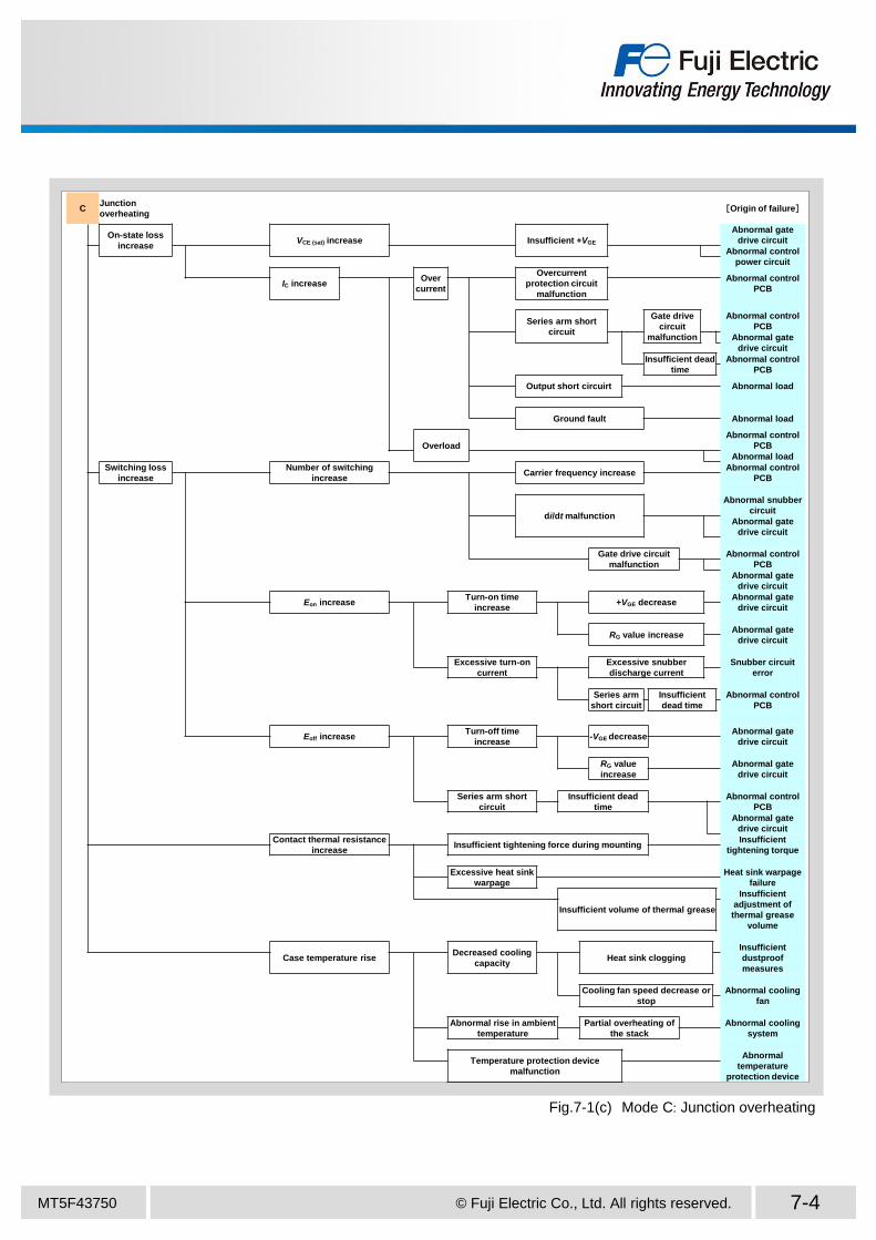
Fig.7-1(c) Mode C: Junction overheating
CJunction
overheating[Origin of failure]
On-state loss
increaseVCE (sat) increase Insufficient +VGE
Abnormal gate
drive circuit
Abnormal control
power circuit
IC increaseOver
current
Overcurrent
protection circuit
malfunction
Abnormal control
PCB
Series arm short
circuit
Gate drive
circuit
malfunction
Abnormal control
PCB
Abnormal gate
drive circuit
Insufficient dead
time
Abnormal control
PCB
Output short circuirt Abnormal load
Ground fault Abnormal load
Overload
Abnormal control
PCB
Abnormal load
Switching loss
increase
Number of switching
increaseCarrier frequency increase
Abnormal control
PCB
di/dt malfunction
Abnormal snubber
circuit
Abnormal gate
drive circuit
Gate drive circuit
malfunction
Abnormal control
PCB
Abnormal gate
drive circuit
Eon increaseTurn-on time
increase+VGE decrease
Abnormal gate
drive circuit
RG value increaseAbnormal gate
drive circuit
Excessive turn-on
current
Excessive snubber
discharge current
Snubber circuit
error
Series arm
short circuit
Insufficient
dead time
Abnormal control
PCB
Eoff increaseTurn-off time
increase-VGE decrease
Abnormal gate
drive circuit
RG value
increase
Abnormal gate
drive circuit
Series arm short
circuit
Insufficient dead
time
Abnormal control
PCB
Abnormal gate
drive circuit
Contact thermal resistance
increaseInsufficient tightening force during mounting
Insufficient
tightening torque
Excessive heat sink
warpage
Heat sink warpage
failure
Insufficient volume of thermal grease
Insufficient
adjustment of
thermal grease
volume
Case temperature riseDecreased cooling
capacityHeat sink clogging
Insufficient
dustproof
measures
Cooling fan speed decrease or
stop
Abnormal cooling
fan
Abnormal rise in ambient
temperature
Partial overheating of
the stack
Abnormal cooling
system
Temperature protection device
malfunction
Abnormal
temperature
protection device
MT5F43750 © Fuji Electric Co., Ltd. All rights reserved. 7-5
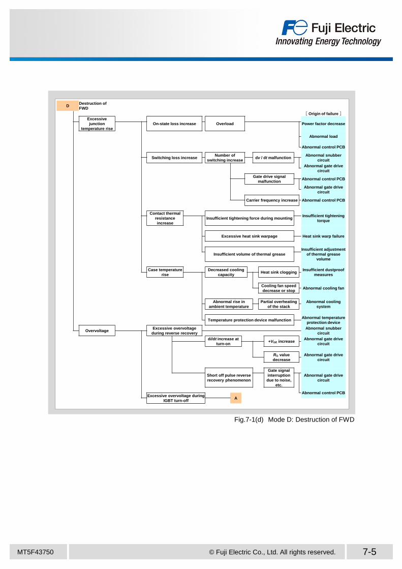
Fig.7-1(d) Mode D: Destruction of FWD
DDestruction of
FWD
[ Origin of failure ]
Excessive
junction
temperature rise
On-state loss increase Overload Power factor decrease
Abnormal load
Abnormal control PCB
Switching loss increaseNumber of
switching increasedv / dt malfunction
Abnormal snubber
circuit
Abnormal gate drive
circuit
Gate drive signal
malfunctionAbnormal control PCB
Abnormal gate drive
circuit
Carrier frequency increase Abnormal control PCB
Contact thermal
resistance
increase
Insufficient tightening force during mountingInsufficient tightening
torque
Excessive heat sink warpage Heat sink warp failure
Insufficient volume of thermal grease
Insufficient adjustment
of thermal grease
volume
Case temperature
rise
Decreased cooling
capacityHeat sink clogging
Insufficient dustproof
measures
Cooling fan speed
decrease or stopAbnormal cooling fan
Abnormal rise in
ambient temperature
Partial overheating
of the stack
Abnormal cooling
system
Temperature protection device malfunctionAbnormal temperature
protection device
OvervoltageExcessive overvoltage
during reverse recovery
Abnormal snubber
circuit
di/dt increase at
turn-on+VGE increase
Abnormal gate drive
circuit
RG value
decrease
Abnormal gate drive
circuit
Short off pulse reverse
recovery phenomenon
Gate signal
interruption
due to noise,
etc.
Abnormal gate drive
circuit
Abnormal control PCBExcessive overvoltage during
IGBT turn-offA
MT5F43750 © Fuji Electric Co., Ltd. All rights reserved. 7-6
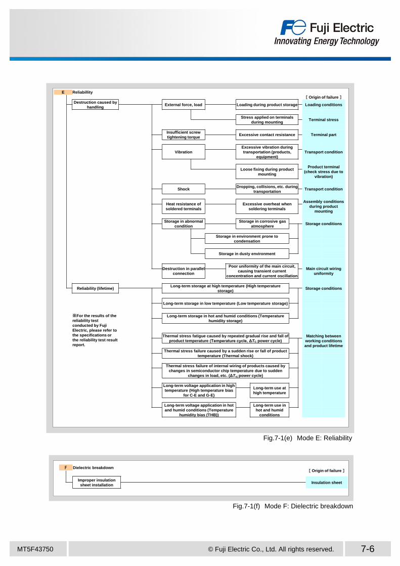
Fig.7-1(e) Mode E: Reliability
Fig.7-1(f) Mode F: Dielectric breakdown
F Dielectric breakdown[ Origin of failure ]
Improper insulation
sheet installationInsulation sheet
E Reliabillity
[ Origin of failure ]Destruction caused by
handlingExternal force, load Loading during product storage Loading conditions
Stress applied on terminals
during mountingTerminal stress
Insufficient screw
tightening torqueExcessive contact resistance Terminal part
Vibration
Excessive vibration during
transportation (products,
equipment)
Transport condition
Loose fixing during product
mounting
Product terminal
(check stress due to
vibration)
ShockDropping, collisions, etc. during
transportationTransport condition
Heat resistance of
soldered terminals
Excessive overheat when
soldering terminals
Assembly conditions
during product
mounting
Storage in abnormal
condition
Storage in corrosive gas
atmosphereStorage conditions
Storage in environment prone to
condensation
Storage in dusty environment
Destruction in parallel
connection
Poor uniformity of the main circuit,
causing transient current
concentration and current oscillation
Main circuit wiring
uniformity
Reliability (lifetime)Long-term storage at high temperature (High temperature
storage)Storage conditions
Long-term storage in low temperature (Low temperature storage)
※For the results of the
reliability test
conducted by Fuji
Electric, please refer to
the specifications or
the reliability test result
report.
Long-term storage in hot and humid conditions (Temperature
humidity storage)
Thermal stress fatigue caused by repeated gradual rise and fall of
product temperature (Temperature cycle, ΔTC power cycle)
Matching between
working conditions
and product lifetime
Thermal stress failure caused by a sudden rise or fall of product
temperature (Thermal shock)
Thermal stress failure of internal wiring of products caused by
changes in semiconductor chip temperature due to sudden
changes in load, etc. (ΔTvj power cycle)
Long-term voltage application in high
temperature (High temperature bias
for C-E and G-E)
Long-term use at
high temperature
Long-term voltage application in hot
and humid conditions (Temperature
humidity bias (THB))
Long-term use in
hot and humid
conditions
MT5F43750 © Fuji Electric Co., Ltd. All rights reserved. 7-7
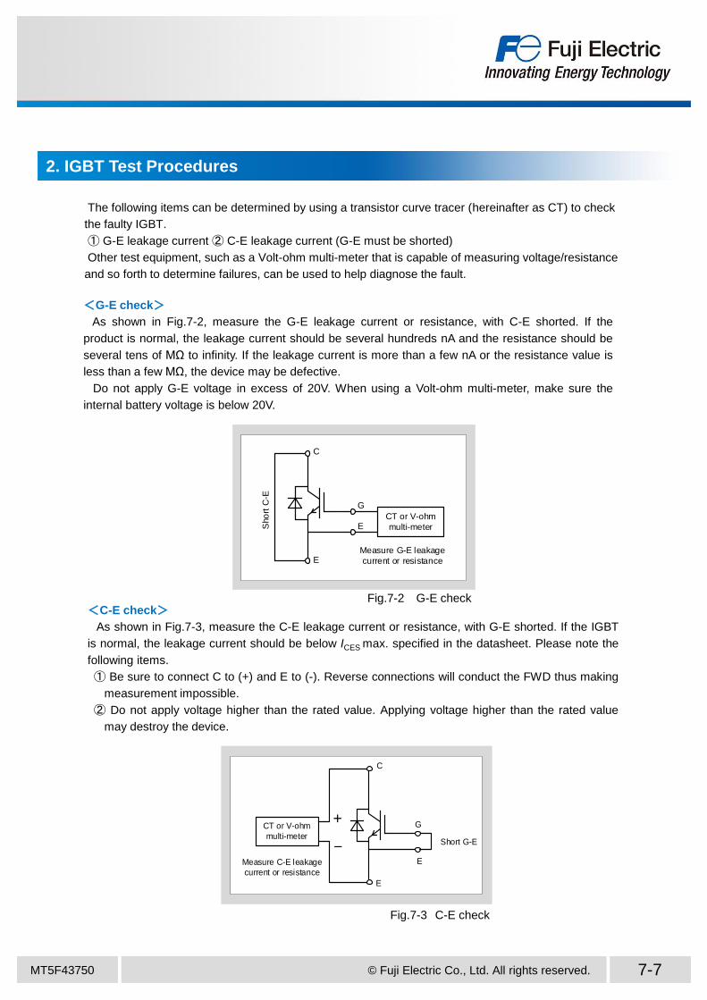
2. IGBT Test Procedures
The following items can be determined by using a transistor curve tracer (hereinafter as CT) to check
the faulty IGBT.
① G-E leakage current ② C-E leakage current (G-E must be shorted)
Other test equipment, such as a Volt-ohm multi-meter that is capable of measuring voltage/resistance
and so forth to determine failures, can be used to help diagnose the fault.
<G-E check>
As shown in Fig.7-2, measure the G-E leakage current or resistance, with C-E shorted. If the
product is normal, the leakage current should be several hundreds nA and the resistance should be
several tens of MΩ to infinity. If the leakage current is more than a few nA or the resistance value is
less than a few MΩ, the device may be defective.
Do not apply G-E voltage in excess of 20V. When using a Volt-ohm multi-meter, make sure the
internal battery voltage is below 20V.
Fig.7-2 G-E check<C-E check>
As shown in Fig.7-3, measure the C-E leakage current or resistance, with G-E shorted. If the IGBT
is normal, the leakage current should be below ICES max. specified in the datasheet. Please note the
following items.
① Be sure to connect C to (+) and E to (-). Reverse connections will conduct the FWD thus making
measurement impossible.
② Do not apply voltage higher than the rated value. Applying voltage higher than the rated value
may destroy the device.
Fig.7-3 C-E check
G
E
C
E
CT or V-ohm
multi-meterSho
rt C
-E
Measure G-E leakage
current or resistance
CT or V-ohm
multi-meter
E
E
G
C
+
-Measure C-E leakage
current or resistance
Short G-E
MT5F43750 © Fuji Electric Co., Ltd. All rights reserved. 7-8
3. Typical Troubles and Troubleshooting
c070-3765-4209
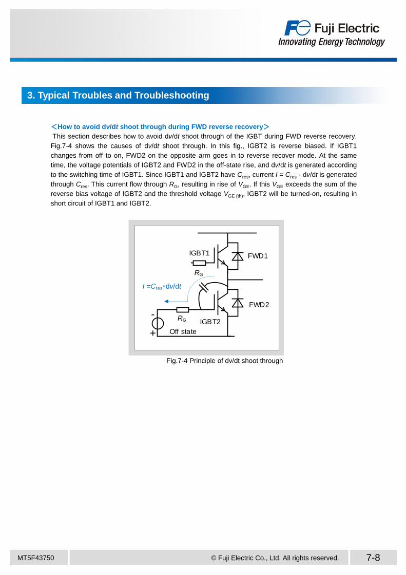
Fig.7-4 Principle of dv/dt shoot through
<How to avoid dv/dt shoot through during FWD reverse recovery>
This section describes how to avoid dv/dt shoot through of the IGBT during FWD reverse recovery.
Fig.7-4 shows the causes of dv/dt shoot through. In this fig., IGBT2 is reverse biased. If IGBT1
changes from off to on, FWD2 on the opposite arm goes in to reverse recover mode. At the same
time, the voltage potentials of IGBT2 and FWD2 in the off-state rise, and dv/dt is generated according
to the switching time of IGBT1. Since IGBT1 and IGBT2 have Cres, current I = Cres · dv/dt is generated
through Cres. This current flow through RG, resulting in rise of VGE. If this VGE exceeds the sum of the
reverse bias voltage of IGBT2 and the threshold voltage VGE (th), IGBT2 will be turned-on, resulting in
short circuit of IGBT1 and IGBT2.
IGBT1
IGBT2
FWD2
FWD1
RG
RG
I =Cres・dv/dt
Off state+
-
MT5F43750 © Fuji Electric Co., Ltd. All rights reserved. 7-9
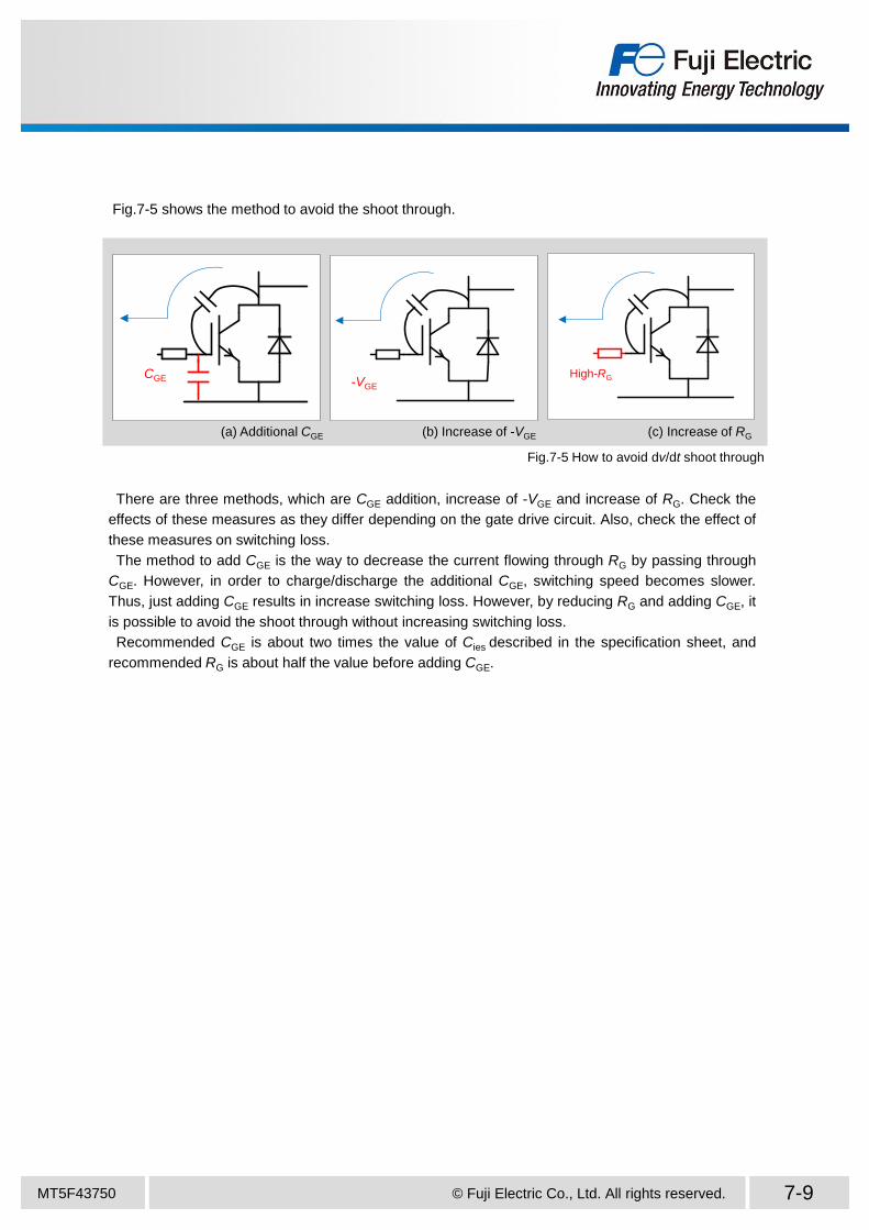
Fig.7-5 How to avoid dv/dt shoot through
There are three methods, which are CGE addition, increase of -VGE and increase of RG. Check the
effects of these measures as they differ depending on the gate drive circuit. Also, check the effect of
these measures on switching loss.
The method to add CGE is the way to decrease the current flowing through RG by passing through
CGE. However, in order to charge/discharge the additional CGE, switching speed becomes slower.
Thus, just adding CGE results in increase switching loss. However, by reducing RG and adding CGE, it
is possible to avoid the shoot through without increasing switching loss.
Recommended CGE is about two times the value of Cies described in the specification sheet, and
recommended RG is about half the value before adding CGE.
Fig.7-5 shows the method to avoid the shoot through.
High-RG-VGE
CGE
(a) Additional CGE (b) Increase of -VGE (c) Increase of RG
MT5F43750
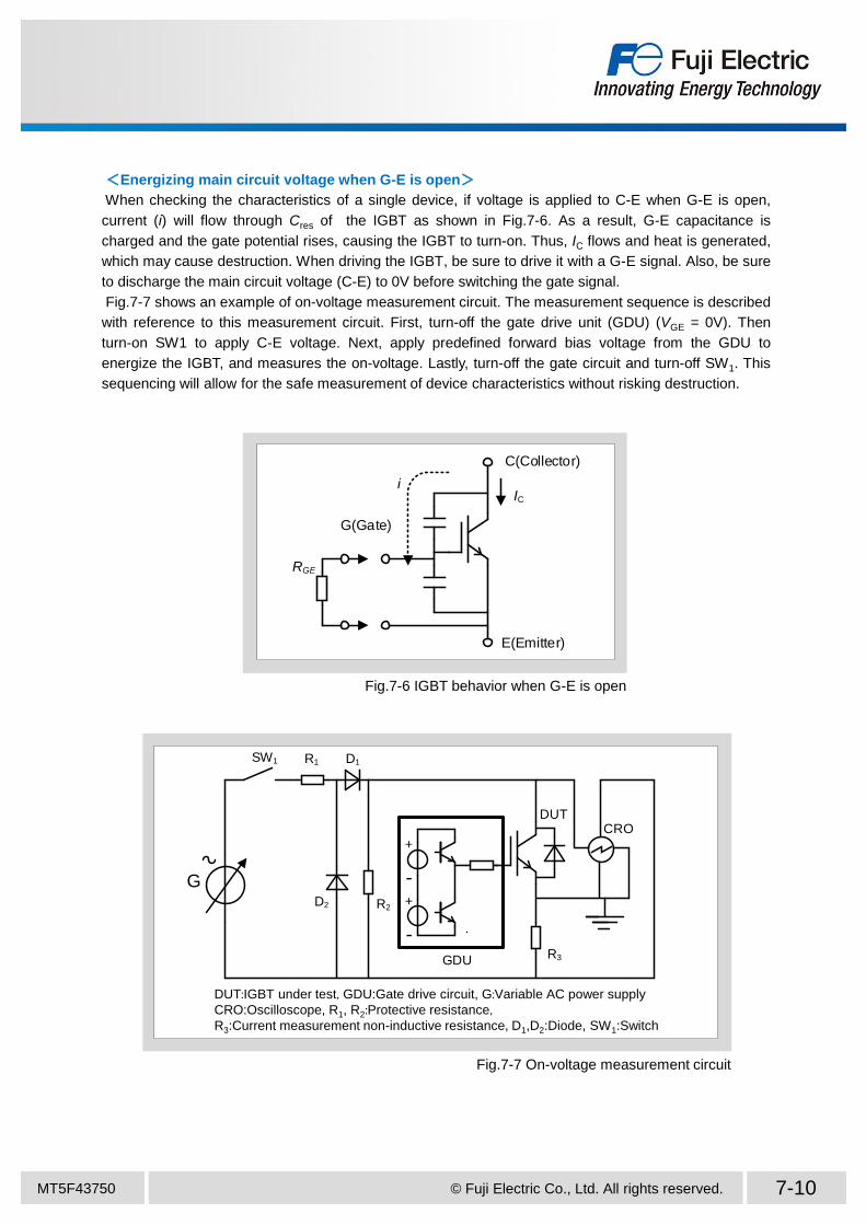
<Energizing main circuit voltage when G-E is open>
When checking the characteristics of a single device, if voltage is applied to C-E when G-E is open,
current (i) will flow through Cres of the IGBT as shown in Fig.7-6. As a result, G-E capacitance is
charged and the gate potential rises, causing the IGBT to turn-on. Thus, IC flows and heat is generated,
which may cause destruction. When driving the IGBT, be sure to drive it with a G-E signal. Also, be sure
to discharge the main circuit voltage (C-E) to 0V before switching the gate signal.
Fig.7-7 shows an example of on-voltage measurement circuit. The measurement sequence is described
with reference to this measurement circuit. First, turn-off the gate drive unit (GDU) (VGE = 0V). Then
turn-on SW1 to apply C-E voltage. Next, apply predefined forward bias voltage from the GDU to
energize the IGBT, and measures the on-voltage. Lastly, turn-off the gate circuit and turn-off SW1. This
sequencing will allow for the safe measurement of device characteristics without risking destruction.
© Fuji Electric Co., Ltd. All rights reserved. 7-10
DUT:IGBT under test, GDU:Gate drive circuit, G:Variable AC power supply
CRO:Oscilloscope, R1, R2:Protective resistance, R3:Current measurement non-inductive resistance, D1,D2:Diode, SW1:Switch
Fig.7-7 On-voltage measurement circuit
Fig.7-6 IGBT behavior when G-E is open
C(Collector)
E(Emitter)
G(Gate)
iIC
RGE
GDU
DUTCRO
R3
G
SW1 R1 D1
D2 R2
+
-+
-
MT5F43750 © Fuji Electric Co., Ltd. All rights reserved. 7-11
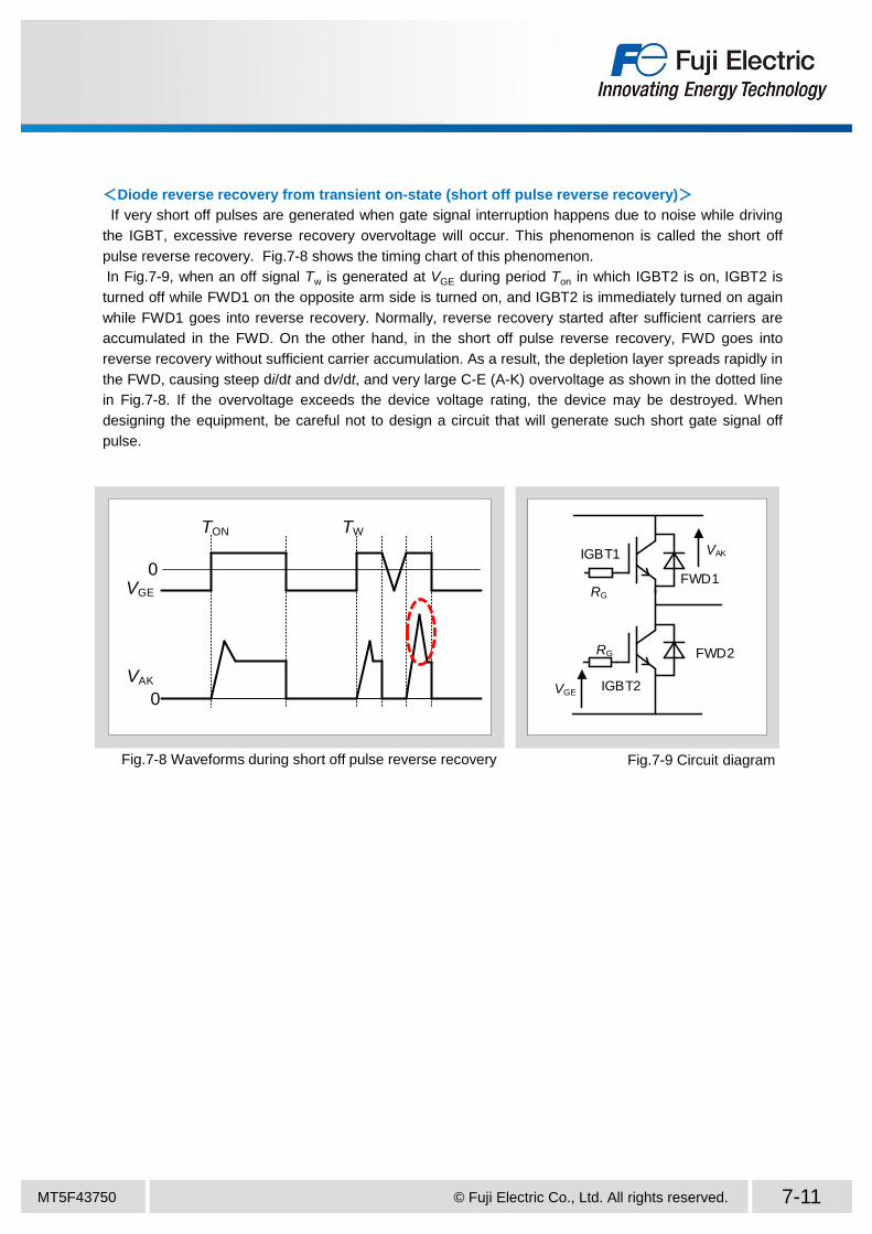
<Diode reverse recovery from transient on-state (short off pulse reverse recovery)>
If very short off pulses are generated when gate signal interruption happens due to noise while driving
the IGBT, excessive reverse recovery overvoltage will occur. This phenomenon is called the short off
pulse reverse recovery. Fig.7-8 shows the timing chart of this phenomenon.
In Fig.7-9, when an off signal Tw is generated at VGE during period Ton in which IGBT2 is on, IGBT2 is
turned off while FWD1 on the opposite arm side is turned on, and IGBT2 is immediately turned on again
while FWD1 goes into reverse recovery. Normally, reverse recovery started after sufficient carriers are
accumulated in the FWD. On the other hand, in the short off pulse reverse recovery, FWD goes into
reverse recovery without sufficient carrier accumulation. As a result, the depletion layer spreads rapidly in
the FWD, causing steep di/dt and dv/dt, and very large C-E (A-K) overvoltage as shown in the dotted line
in Fig.7-8. If the overvoltage exceeds the device voltage rating, the device may be destroyed. When
designing the equipment, be careful not to design a circuit that will generate such short gate signal off
pulse.
c070-3765-4209
Fig.7-9 Circuit diagram
c070-3765-4209
Fig.7-8 Waveforms during short off pulse reverse recovery
IGBT1
IGBT2
FWD2
FWD1RG
RG
VGE
VAK
0
0VGE
VAK
TON TW
MT5F43750 © Fuji Electric Co., Ltd. All rights reserved. 7-12
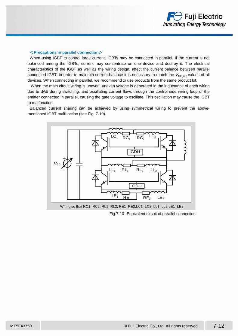
Fig.7-10 Equivalent circuit of parallel connection
Wiring so that RC1=RC2, RL1=RL2, RE1=RE2,LC1=LC2, LL1=LL2,LE1=LE2
<Precautions in parallel connection>
When using IGBT to control large current, IGBTs may be connected in parallel. If the current is not
balanced among the IGBTs, current may concentrate on one device and destroy it. The electrical
characteristics of the IGBT as well as the wiring design, affect the current balance between parallel
connected IGBT. In order to maintain current balance it is necessary to match the VCE(sat) values of all
devices. When connecting in parallel, we recommend to use products from the same product lot.
When the main circuit wiring is uneven, uneven voltage is generated in the inductance of each wiring
due to di/dt during switching, and oscillating current flows through the control side wiring loop of the
emitter connected in parallel, causing the gate voltage to oscillate. This oscillation may cause the IGBT
to malfunction.
Balanced current sharing can be achieved by using symmetrical wiring to prevent the above-
mentioned IGBT malfunction (see Fig. 7-10).
GDU
VCC
LC1 RC1 RC2LC2
LL1 RL1 RL2 LL2
LE1 RE1 LE2RE2
+
-
GDU
MT5F43750 © Fuji Electric Co., Ltd. All rights reserved. 7-13
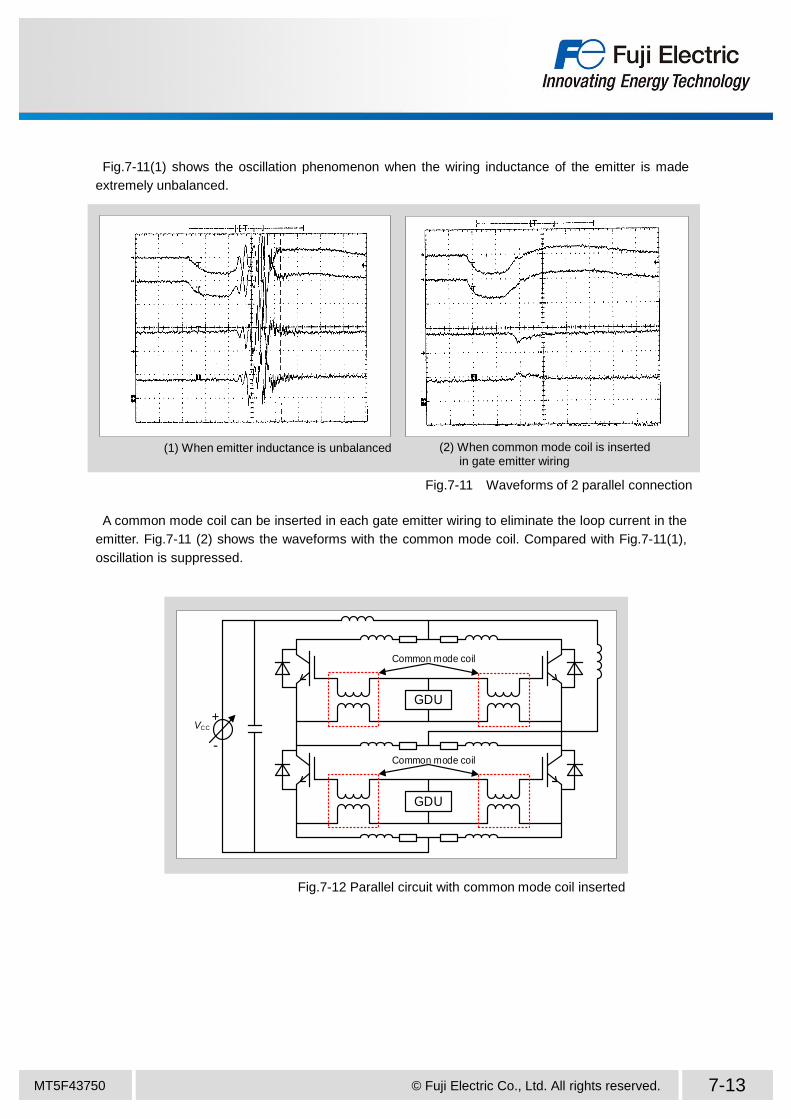
A common mode coil can be inserted in each gate emitter wiring to eliminate the loop current in the
emitter. Fig.7-11 (2) shows the waveforms with the common mode coil. Compared with Fig.7-11(1),
oscillation is suppressed.
Fig.7-12 Parallel circuit with common mode coil inserted
Fig.7-11(1) shows the oscillation phenomenon when the wiring inductance of the emitter is made
extremely unbalanced.
(1) When emitter inductance is unbalanced (2) When common mode coil is inserted
in gate emitter wiring
Fig.7-11 Waveforms of 2 parallel connection
iG1
iG2
iC11
iC21
iG1
iG2
iC11
iC21
iG1
iG2
iC11
iC21
iG1
iG2
iC11
iC21
+
-
GDU
GDU
VCC
Common mode coil
Common mode coil