Embed Size (px)
Citation preview
J.-P. Teyssier. Characterization of high power microwave transistors
Доклады ТУСУРа, № 2 (22), часть 1, декабрь 2010
127
UDC 621.382.323 J.-P. Teyssier
Characterization of high power microwave transistors
This paper describes up-to-date nonlinear measurements techniques for characterization and modelling of high power microwave transistors, from pulsed I(V) to time domain load-pull measurements. The described toolkit is well-suited for study of weak nonlinear regimes of transistors as long as long-term memory effects taking place into transistors. Keywords: characterization, high power microwave transistor, microwave measurements.
Introduction The transistor modeling task interacts with the real transistor through a relatively large
set of experiments and extracts a mathematical model from the measured data. This model describes how the transistor behaves under a wide range of excitation signals and operating conditions. The goal of transistor characterization is usually to get a good transistor model, and the relevant starting point consists in gathering knowledge about the transistor. It means to get some physical parameters of the transistor in order to have a minimum idea of its behavior, and then to applies a variety of signals to the transistor terminals and meas-ures quantities that are related to the voltage and current waveforms. The quantities that are measured can be instantaneous values of the voltages and currents, but can also be other de-rived quantities like S-parameters, or the time averaged values of voltages and currents. The trick is to apply a minimum number of excitation signals that allows determining the tran-sistor characteristics in all its working areas; this is an obvious but sometime insufficient requirement for the determination of all unknown parameters of the model. Note that the signals that are used for model extraction are usually quite simple and much different from the signals that the transistor will see in a final application.
The next task consists in verifying assumptions on the schematics and/or mathematical structure of the model by performing model validation experiments. The idea of model vali-dation is to provide excitation signals that are as close as possible to the signals that will be seen by the transistor in its final application, and to verify whether the model can predict the measured results. Load-pull and time domain load-pull large signal experiments are some of the most famous verification techniques at transistor or amplifier level. A usual extension of large signal measurements consists in applying signals more complex than a single tone CW frequency: multi-tone or modulated signals. The transistor's long term memory effects are of great importance; with such more complex signals the capability of the model to pre-dict them can be checked.
So power transistor characterization classically consists in two steps: measurements de-voted to model extraction, and measurements devoted to model verification. A new tendency now appears with the new family of behavioral models (like the recent X-Parameters models), where the experiments to build the model are very close to experiments devoted to model verification, i.e. microwave RF transistor nonlinear model is obtained from large signal mi-crowave measurements.
A reliable and accurate microwave power transistor characterization procedure is still a difficult task. The main difficulties are already included in the previous sentence: «micro-wave» and «power».
Due to the microwave frequencies, even a very low intrinsic or extrinsic capacitor will drive a very significant current, and any parasitic inductance (like the very small parasitic inductor of via holes) will present significant RF impedance. The DC I(V) characterization are sufficient to get the nonlinear behavior of the main transistor effects (usually output current versus voltages and diodes characteristics), but DC I(V) experiments do not provide any data about the reactive elements of the transistor under test. Moreover, at microwave frequencies, the usual voltage and current values are not easy to measure due to the wave propagation physics, but the microwave absolute or relative power level and the relative phases are more straightforward data. As a consequence, the scattering parameter (S-parameter) measurements are obviously the measurement techniques of choice for microwave devices. The inductive and capacitive behaviors will be extracted from S-parameters.
High power transistors are converting DC power into microwave power. Unfortunately transistors are also converting a significant portion of the DC power into heat, despite the use of new optimized working class of amplifiers. In many practical applications only about
ИЗМЕРЕНИЕ И ХАРАКТЕРИЗАЦИЯ ПАРАМЕТРОВ СВЧ-МАТЕРИАЛОВ И УСТРОЙСТВ
Доклады ТУСУРа, № 2 (22), часть 1, декабрь 2010
128
half of the DC power is converted into microwave power, the other half is converted into heat. The consequence is that power transistors are seeing a wide range of temperatures dur-ing the characterization measurements as well as during their operation; moreover the tem-perature is not a unique transistor parameter but a distribution inside the transistor and its fingers. Many of the elements of transistor's equivalent scheme are very sensitive to tem-perature. The temperature behavior linked to the dissipated power acts like as long term memories. Up-to-date device models will describe this thermal phenomenon by introducing one or several temperatures as explicit parameters in the model equations. As a direct conse-quence for the transistor characterization process, the temperature must be measured and kept as much as possible under control or, depending on the experiment methodlogy, swept during all the other kinds of electrical measurements. Pulsed measurements (including pulsed I(V), pulsed S-parameter and pulsed load-pull) will be a suitable answer to that issue.
This paper will describe in depth the following high power microwave transistor measurement techniques: pulsed I(V); pulsed S-parameters; load-pull and source-pull measurement; time domain load pull waveforms measurements, and will finally debate about the tendencies and future developments of nonlinear measurements.
Pulsed I(V) Measurements I(V) characteristics are the starting point for the transistor effect characterization,
providing the well-known drain or collector current characteristics versus voltages. These characteristics are very sensitive to the temperature; it's a linked loop problem because the temperature changes by self-heating when the transistor under test drives some current. The simplest way to get data would be to directly measure the temperature dependent voltage current relationship. Two simple measurement methods can then be imagined: keeping the temperature under control and measure I(V) relationships for several temperatures, or measuring all the parameters V, I , T simultaneously. Practically speaking, both approaches are difficult to apply without assumptions and limitations.
In practice we can apply a particular {VCE , IB} or {VGS, VDS} (the commands) and a temperature T and we make sure that we measure {VBE ,IC} or {IGS, IDS}(the responses) before the temperature has significantly changed. Such a measurement is referred to as «isothermal». From the hardware perspective this implies that we need to have means to control the temperature of the transistor, like a thermal chuck, such that it has a temperature T when we start the experiment, and that we need to have the capability to apply the commands and make a quick measurement of the results before there is any significant change of the device temperature. Since we want to do more than one measurement, we switch the commands off as quickly as possible after the experiment. We then wait until we are sure that the temperature has returned back to T before performing a subsequent measurement. This process is called pulsed I(V) or PIV characterization. Note that there are many ways to perform pulsed measurements. A lot of insight into the trapping behavior as well as the thermal behavior can be gained by not only changing the command values during the pulse, but by also changing the initial bias values.
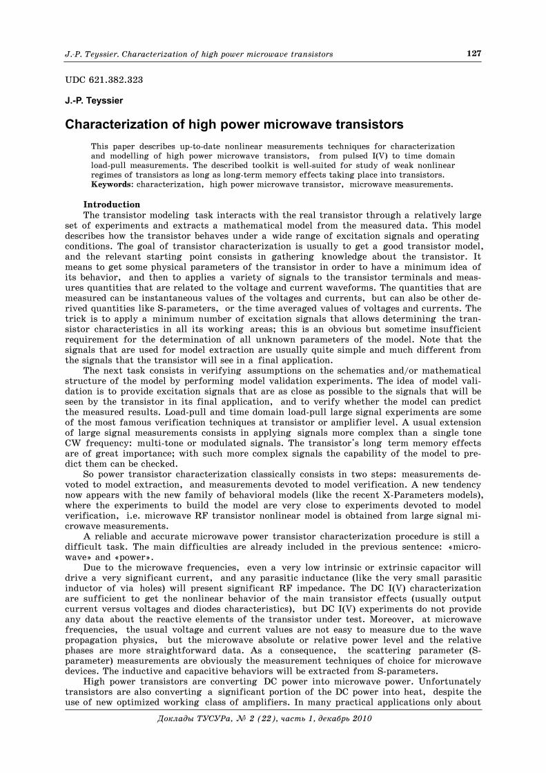
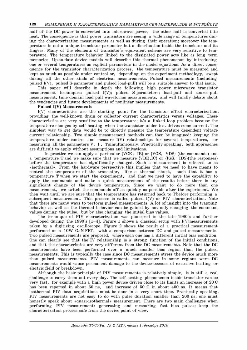
The technique of PIV characterization was pioneered in the late 1980's and further developed during the 1990's [1–4]. Figure 1 shows a classical setup with I(V)measurements taken by a digitizing oscilloscope. Figure 2 shows the result of a practical measurement performed on a 10W GaN FET, with a comparison between DC and pulsed measurements. Two pulsed measurements are proposed, where each one has a different initial bias condition. One can clearly see that the IV relationship is a strong function of the initial conditions, and that the characteristics are very different from the DC measurements. Note that the DC measurements have been performed over a much smaller bias region than the pulsed measurements. This is typically the case since DC measurements stress the device much more than pulsed measurements. PIV measurements can measure in some regions were DC measurements would cause permanent damage to the device because of excessive heating or electric field or breakdown.
Although the basic principle of PIV measurements is relatively simple, it is still a real challenge to carry them out every day. The self-heating phenomenon inside transistor can be very fast, for example with a high power device driven close to its limits an increase of 20 C has been reported in about 50 ns, and increase of 50 C in about 400 ns. It means that isothermal PIV data acquisitions must be done in a very short time. Practically speaking, PIV measurements are not easy to do with pulse duration smaller than 200 ns; one must honestly speak about «quasi-isothermal» measurement. There are two main challenges when performing PIV measurement: generating and measuring fast bias pulses; keep the characterization process safe from the device point of view.
J.-P. Teyssier. Characterization of high power microwave transistors
Доклады ТУСУРа, № 2 (22), часть 1, декабрь 2010
129
Fig. 1. PIV setup with 2 pulsers and measurements taken
with a digitizing oscilloscope
Fig. 2. PIVmeasurement of a 10W GaN device: comparison of DC (lines up to 20 Volts) and pulsed
characteristics, starting from (VDS, ID) = (0 V, 0 mA) for highest Id currents and from (45 V, 100 mA) for smaller Id currents
The first challenge consists in generating and measuring the fast high power bias
excitation pulses, which need transition times that are only a fraction of the pulse width, let's say 30 ns. The very new high power microwave transistors are now handling very high current and voltages. Only very recent MOSFET or GaN based pulsers can deliver pulses up to 300 V and 10 A. When performing such measurements, one has to be very cautious about the presence of parasitic inductive and capacitive elements. Because of the hard slopes of the voltage and the current pulses, parasitic inductive and capacitive elements can easily cause ringing effects in the applied pulses. In fact one needs a really careful design of the cabling between the pulses and the transistors; the good practice is to locate the pulsed bias generators as close as possible to the transistor terminals. A complete characterization of a transistor requires the application of extreme pulsed bias conditions, for example near the transistor breakdown area. Under such conditions, especially when using a low impedance generator, sudden breakdown effects may generate a spectacularly big current spike through the transistor, with an immediate destruction of the device and, sometimes of the pulser. To prevent this from happening, one can introduce a resistive network between the transistor and the pulser. The resistances will then provide a robust protection for breakdown current spikes. Moreover, this network provides access for the measurements and allows changing the bias impedance depending on the device limits. Such networks can be adjusted to reduce/avoid parametric oscillations of a particular device. An example resistive network is shown in Fig. 1.
Pulsed S-parameters Measurements As said before, microwave transistors cannot only be described by a set of static I(V)
relationships. The model will also contain capacitive and inductive effects that need to be characterized.
ИЗМЕРЕНИЕ И ХАРАКТЕРИЗАЦИЯ ПАРАМЕТРОВ СВЧ-МАТЕРИАЛОВ И УСТРОЙСТВ
Доклады ТУСУРа, № 2 (22), часть 1, декабрь 2010
130
Many of these are bias-dependent, like the famous nonlinear Cgs capacitor. The idea is then to measure bias dependent S-parameters and to convert the S-parameters into Y-parameters. The bias dependent Y-parameters are containing information on the partial derivatives of the charge storage functions. The modelling task integrates the measured Y-parameters and can reconstruct the unknown charge storage functions. It is not hard to imagine that a similar approach will also give information on the inductive effects. The conclusion is that bias dependent S-parameters are necessary for determining the nonlinear reactive elements of the transistor.
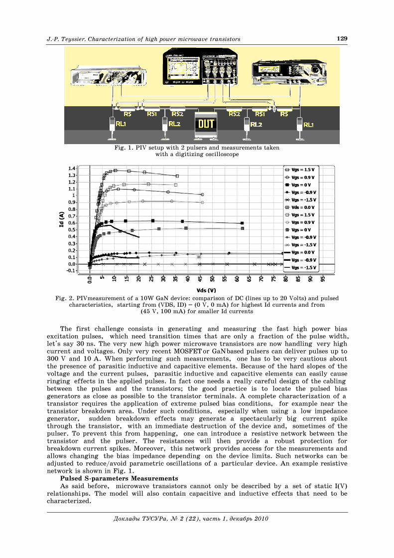
Moreover many of these reactive elements are also modified by the temperature. The idea is then to also measure the bias dependent S-parameters under controlled isothermal conditions. Such measurements are called isothermal pulsed-bias S-parameter measurements. Adding and synchronizing S-parameter capability to PIV measurements was pioneered in the early 1990's [2, 3, 5] and is still an interesting literature topic today [6, 7]. A practical example of pulsed bias S-parameter measurements of a 20 W FET is shown in Fig. 3.
Fig. 3. Pulsed bias S-parameters measurements, S-Parameters for 2 different pulsed points
The pulsed S-parameter measurements are very challenging because they need to be made
under fast pulsed conditions. In 1990, the VNA Anritsu Wiltron 360-PS20 was able to meas-ure RF pulses as short as 100 ns, but not without a severe desensitization that was propor-tional to the duty cycle. It was based on a high Q filtering at intermediate frequency. This VNA was the only one on the shelf with the capability to do very fast RF measurements. To-day, improved ways of measuring pulsed scattering parameters have become available with the advent of a new generation of VNAs. In addition to having better hardware, the dy-namic range of pulsed measurements is further improved, but there is still a desensitization function of the duty cycle. Nevertheless, it is now possible to make 0.001% duty cycle S-parameter measurements in the X-band with a dynamic range better than 50 dB.
Another weak point for synchronized PIV and pulsed S-parameters setups is the electric separation of LF and RF frequency domains: the bias tee. The requirements for these passive components are extreme: wideband RF on one hand, very large voltage and current for the bias path on the other hand, in addition with a wide low frequency bandwidth in order to keep the PIV short pulse capability. The bias tee is frequently one of the most restraining components of pulsed setups.
PIV combined with pulsed S-parameters measurements are frequently made under extrin-sic temperature control, with a thermo-chuck or a thermal chamber. Such setups have pro-vided data for parameters extraction of a large number of good quality microwave high power transistor models all over the world.
J.-P. Teyssier. Characterization of high power microwave transistors
Доклады ТУСУРа, № 2 (22), часть 1, декабрь 2010
131
Load-pull Measurements Circuit designers need to simulate their transistors under real operating conditions. So
the question is: will a model extracted from quite simple signals (PIV and pulsed S-parameters for several temperatures) correctly predict the transistor behavior inside an amplifier? To check a model reliability, the device must be experimentally characterized under more realistic operating conditions and the results have to be compared with the model prediction. Model validation is done by stimulating a transistor with excitation signals that are very similar to the signals that the device will experience in a power amplifier, and by measuring certain characteristics that can be derived from the response signals such as gain and power added efficiency. The most significant difference between a validation setup and the pulsed-bias S-parameter system is the power of the applied microwave signals. The validation system needs to apply microwave signals able to sweep across the whole transistor operating region, whereas a pulsed-bias S-parameter system will only use relatively small microwave signals and will cover the transistor operating region by means of pulsing the bias. Moreover, a pulsed-bias S-parameter system will usually terminate the transistor terminals into a 50 Ohm load. In microwave power amplifiers, the transistor output is terminated in a wide range of impedances. Finally, a validation system needs to provide three main functions: exciting the transistor with sufficient microwave power, controlling the output impedance, and measuring the response signal of the transistor. Controlling the output impedance is often referred to as «load-pull». Note that one sometimes also controls the impedance of the signal generator, this is called «source-pull».
As described in [8], load-pull systems are typically classified into two main categories: active and passive. In a passive load-pull system, the load impedance is controlled by passive tuners. The passive tuner is usually mechanical, whereby a metal part is moving in a waveguide in order to create controllable reflections. A good example is described in [9]. The major drawback of using a passive structure is that one cannot compensate for any power that is dissipated between the device under test and the passive structure that generates the controllable reflection. This power dissipation inevitably occurs in all components that are placed between the transistor terminal and the tuning elements such as probes, cables, couplers, diplexers... As a result, the maximum amplitude of the reflection coefficient, as seen by the transistor, will always be smaller than one. Depending on the amount of inevitable losses in the measurement setup, the maximum amplitude of the reflection coefficient may become too small for properly loading the transistor.
This problem may be solved by using so-called active load-pull setups. These are setups in which one introduces one or more amplifiers to generate wave signals that are sent towards the device-under-test output terminals. The amplifier can potentially compensate for any losses and generate reflection coefficients with amplitudes equal to and even bigger than one. A good example, illustrating the problems and benefits of active load-pull is described in [10]. The power handling capability of active load-pull setup is limited by the amplifier that is used.
In contrast to the active load-pull setups, the maximum power handling capability and frequency range of passive load-pull setup is only limited by passive structures like cables, couplers, etc... Passive tuners typically operate across multiple octaves and can handle power levels larger than 100 watts. Today, the vast majority of the load-pull setups use passive mechanical tuners. Note that the typical mismatch of a GaN transistor is low and suitable for most simple mechanical tuners, in contrast with silicon LDMOS transistors which exhibit strong mismatches.
An example of a classic load-pull setup is depicted in Fig. 3. Load and source tuners are placed as close as possible to the transistor under test. The two tuners are providing a whole range of possible input and output impedances. The input signal comes from a synthesizer, often boosted by a power amplifier. A vector network analyzer (VNA) and a power meter are used to measure the RF signals. A bias supply and monitoring system are also present. The setup can stimulate the transistor with a realistic, high power microwave signal while at the same time presenting realistic output impedances. Note that the power reading is taken after the tuner and not at the transistor output terminal. The transistor performance can only be calculated by using a combination of the power meter reading with the VNA measurements, the measured bias voltages and currents and, finally, the S-parameters of the tuners depending on their settings. The tuner S-parameters are stored in lock-up tables previously obtained with a time-consuming tuner calibration procedure.
There exist many variations of the load-pull system depicted in Fig. 3. For example, some systems are simpler because they do not have the input coupler and VNA. Some systems
ИЗМЕРЕНИЕ И ХАРАКТЕРИЗАЦИЯ ПАРАМЕТРОВ СВЧ-МАТЕРИАЛОВ И УСТРОЙСТВ
Доклады ТУСУРа, № 2 (22), часть 1, декабрь 2010
132
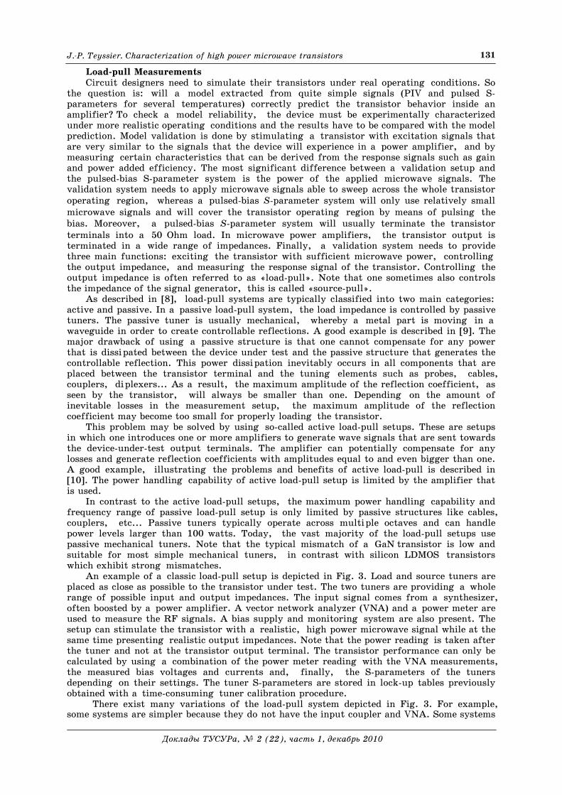
are more complex, for example, using a spectrum analyzer instead of a power meter. Of course the simpler systems provide less information on the transistor behavior than the more complex ones. If one eliminates the input coupler and VNA, for example, it is impossible to determine the power absorbed at the input of the transistor. Adding a spectrum analyzer, on the other hand, allows you to measure the amplitude of the harmonics.
Fig. 4. Simple passive load-pull and source-pull setup
Most classical load-pull systems control the load impedance and perform power measurements only at the input signal fundamental frequency. Any large-signal excitation of the power transistor will not only generate output power at the fundamental frequency, but also at multiples of the fundamental frequency, the harmonics. The overall behavior of the transistor will not only depend on the load impedance at the fundamental frequency but will also depend on the load impedances at the harmonic frequencies. Some load-pull systems control the load impedance at the second and even the third harmonic frequencies [11, 12]. Such systems are called harmonic load-pull systems.
A frequent extension of load-pull systems consists in applying modulated signals. Signals with two tones are of great interest as one can measure some intermodulation characteristics or memory effects. Pulsed bias and/or pulsed RF signals might be required if the target application of the transistor under test is pulsed.
Time Domain Load-pull waveforms measurements Classic load-pull systems allow one to verify whether a model can accurately predict
power levels under load-pull operating conditions. A more in-depth model validation for highly nonlinear effects can be achieved by measuring the time-domain voltage and current waveforms under realistic large-signal operating conditions, and by comparing them with the time-domain waveforms resulting from a simulation.
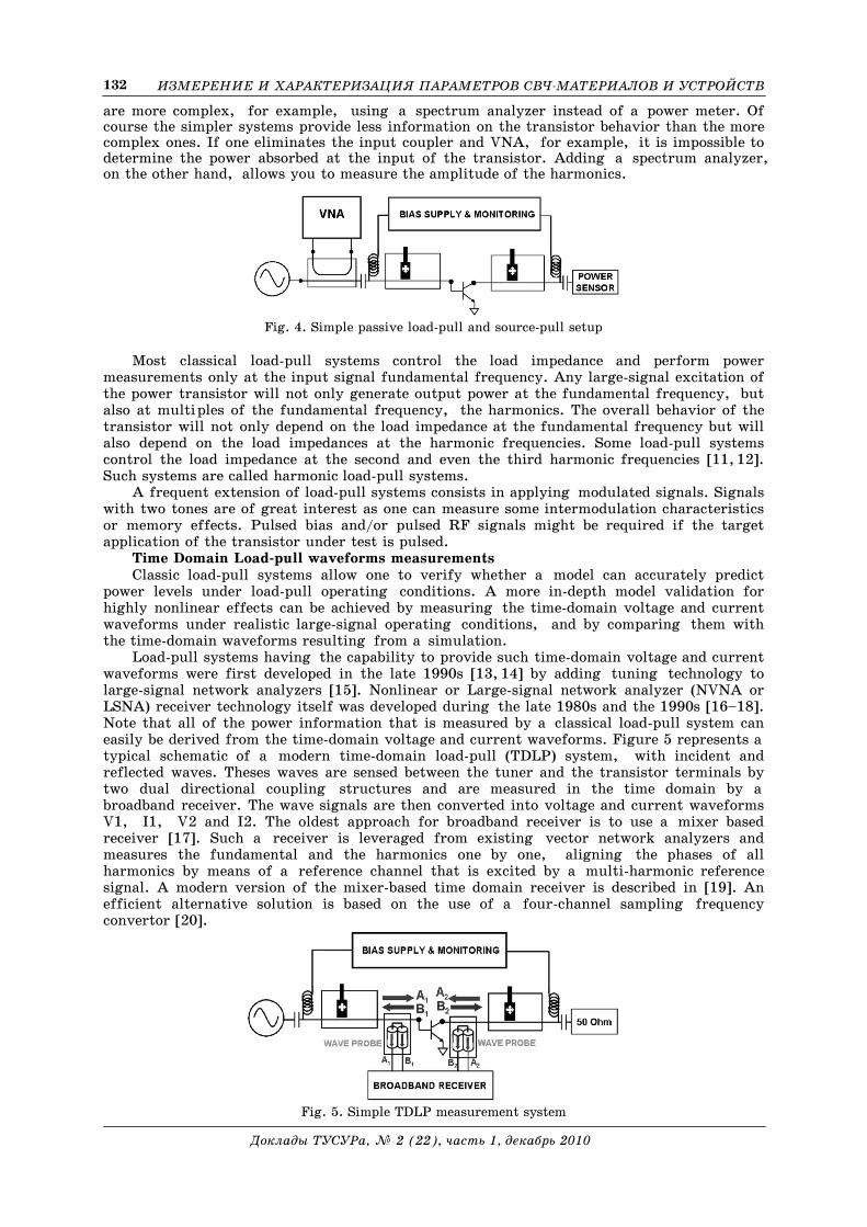
Load-pull systems having the capability to provide such time-domain voltage and current waveforms were first developed in the late 1990s [13, 14] by adding tuning technology to large-signal network analyzers [15]. Nonlinear or Large-signal network analyzer (NVNA or LSNA) receiver technology itself was developed during the late 1980s and the 1990s [16–18]. Note that all of the power information that is measured by a classical load-pull system can easily be derived from the time-domain voltage and current waveforms. Figure 5 represents a typical schematic of a modern time-domain load-pull (TDLP) system, with incident and reflected waves. Theses waves are sensed between the tuner and the transistor terminals by two dual directional coupling structures and are measured in the time domain by a broadband receiver. The wave signals are then converted into voltage and current waveforms V1, I1, V2 and I2. The oldest approach for broadband receiver is to use a mixer based receiver [17]. Such a receiver is leveraged from existing vector network analyzers and measures the fundamental and the harmonics one by one, aligning the phases of all harmonics by means of a reference channel that is excited by a multi-harmonic reference signal. A modern version of the mixer-based time domain receiver is described in [19]. An efficient alternative solution is based on the use of a four-channel sampling frequency convertor [20].
Fig. 5. Simple TDLP measurement system
J.-P. Teyssier. Characterization of high power microwave transistors
Доклады ТУСУРа, № 2 (22), часть 1, декабрь 2010
133
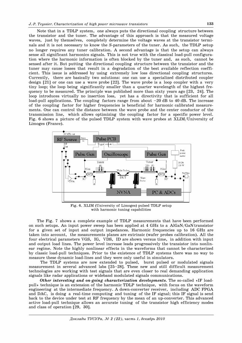
Note that in a TDLP system, one always puts the directional coupling structure between the transistor and the tuner. The advantage of this approach is that the measured voltage waves, just by themselves, completely determine the voltage waves at the transistor termi-nals and it is not necessary to know the S-parameters of the tuner. As such, the TDLP setup no longer requires any tuner calibration. A second advantage is that the setup can always sense all significant harmonics signals. This is not true with the classical load-pull configura-tion where the harmonic information is often blocked by the tuner and, as such, cannot be sensed after it. But putting the directional coupling structure between the transistor and the tuner may cause losses that result in a degradation of the best available reflection coeffi-cient. This issue is addressed by using extremely low loss directional coupling structures. Currently, there are basically two solutions: one can use a specialized distributed coupler design [21] or one can use a wave probe [22]. The wave probe is a loop coupler with a very tiny loop; the loop being significantly smaller than a quarter wavelength of the highest fre-quency to be measured. The principle was published more than sixty years ago [23, 24]. The loop introduces virtually no insertion loss, yet has a directivity that is sufficient for all load-pull applications. The coupling factors range from about –20 dB to 40 dB. The increase of the coupling factor for higher frequencies is beneficial for harmonic calibrated measure-ments. One can control the distance between the wave probe and the center conductor of the transmission line, which allows optimizing the coupling factor for a specific power level. Fig. 6 shows a picture of the pulsed TDLP system with wave probes at XLIM/University of Limoges (France).
Fig. 6. XLIM (University of Limoges) pulsed TDLP setup
with harmonic tuning capabilities
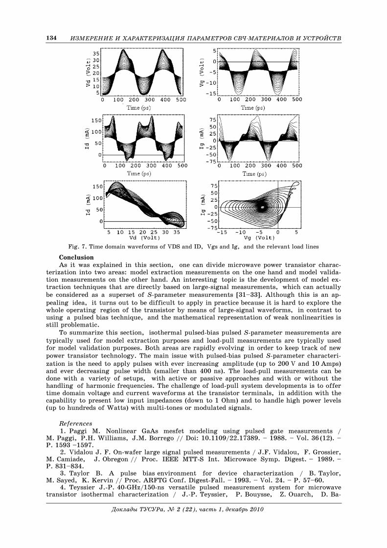
The Fig. 7 shows a complete example of TDLP measurements that have been performed
on such setups. An input power sweep has been applied at 4 GHz to a AlGaN/GaN transistor for a given set of input and output impedances. Harmonic frequencies up to 16 GHz are taken into account, the measurements planes are extrinsic (wafer probes calibration). All the four electrical parameters VGS, IG, VDS, ID are shown versus time, in addition with input and output load lines. The power level increase leads progressively the transistor into nonlin-ear regime. Note the highly nonlinear effects in the waveforms that cannot be characterized by classic load-pull techniques. Prior to the existence of TDLP systems there was no way to measure these dynamic load-lines and they were only useful in simulators.
The TDLP systems are now extended to pulsed, burst pulsed or modulated signals measurement in several advanced labs [25–28]. These new and still difficult measurement technologies are working with test signals that are even closer to real demanding application signals like radar applications or wideband modulated signals communications.
Other interesting and on-going characterization developments. The so-called «IF load-pull» technique is an extension of the harmonic TDLP technique, with focus on the waveform engineering at the intermediate frequency. A down-converter receiver, including ADC FPGA and DAC, is doing a real-time computing and tuning of the IF signal; this IF signal is send back to the device under test at RF frequency by the mean of an up-converter. This advanced active load-pull technique allows an accurate tuning of the transistor high efficiency modes and class of operation [29, 30].
ИЗМЕРЕНИЕ И ХАРАКТЕРИЗАЦИЯ ПАРАМЕТРОВ СВЧ-МАТЕРИАЛОВ И УСТРОЙСТВ
Доклады ТУСУРа, № 2 (22), часть 1, декабрь 2010
134
Fig. 7. Time domain waveforms of VDS and ID, Vgs and Ig, and the relevant load lines
Conclusion As it was explained in this section, one can divide microwave power transistor charac-
terization into two areas: model extraction measurements on the one hand and model valida-tion measurements on the other hand. An interesting topic is the development of model ex-traction techniques that are directly based on large-signal measurements, which can actually be considered as a superset of S-parameter measurements [31–33]. Although this is an ap-pealing idea, it turns out to be difficult to apply in practice because it is hard to explore the whole operating region of the transistor by means of large-signal waveforms, in contrast to using a pulsed bias technique, and the mathematical representation of weak nonlinearities is still problematic.
To summarize this section, isothermal pulsed-bias pulsed S-parameter measurements are typically used for model extraction purposes and load-pull measurements are typically used for model validation purposes. Both areas are rapidly evolving in order to keep track of new power transistor technology. The main issue with pulsed-bias pulsed S-parameter characteri-zation is the need to apply pulses with ever increasing amplitude (up to 200 V and 10 Amps) and ever decreasing pulse width (smaller than 400 ns). The load-pull measurements can be done with a variety of setups, with active or passive approaches and with or without the handling of harmonic frequencies. The challenge of load-pull system developments is to offer time domain voltage and current waveforms at the transistor terminals, in addition with the capability to present low input impedances (down to 1 Ohm) and to handle high power levels (up to hundreds of Watts) with multi-tones or modulated signals.
References 1. Paggi M. Nonlinear GaAs mesfet modeling using pulsed gate measurements /
M. Paggi, P.H. Williams, J.M. Borrego // Doi: 10.1109/22.17389. – 1988. – Vol. 36 (12). – P. 1593 –1597.
2. Vidalou J. F. On-wafer large signal pulsed measurements / J.F. Vidalou, F. Grossier, M. Camiade, J. Obregon // Proc. IEEE MTT-S Int. Microwace Symp. Digest. – 1989. – P. 831–834.
3. Taylor B. A pulse bias environment for device characterization / B. Taylor, M. Sayed, K. Kervin // Proc. ARFTG Conf. Digest-Fall. – 1993. – Vol. 24. – P. 57–60.
4. Teyssier J.-P. 40-GHz/150-ns versatile pulsed measurement system for microwave transistor isothermal characterization / J.-P. Teyssier, P. Bouysse, Z. Ouarch, D. Ba-
J.-P. Teyssier. Characterization of high power microwave transistors
Доклады ТУСУРа, № 2 (22), часть 1, декабрь 2010
135
rataud, T. Peyretaillade, R. Quere // Doi: 10.1109/ 22.739281. – 1998. – Vol. 46(12). – P. 2043–2052.
5. Parker A. Determining timing for isothermal pulsed-bias S-parameter measurements / A. Parker, J. Scott, J. Rathmell, M. Sayed // Proc. IEEE MTT-S Int. Microwave Symp. Digest. – 1996. – Vol. 3. –P. 1707–1710.
6. Aaen P. Characterization of RF and Microwave Power FETs / P. Aaen, J.A. Pla, J. Wood. – Cambridge Press, 2007.
7. Betts L. Tracking advances in pulsed s-parameters measurements / L. Betts // Mi-crowave and RF Journal. – 2007. – № 9. – P. 23–28.
8. Deshours F. Experimental comparison of load-pull measurement systems for nonlinear power transistor characterization / F. Deshours, E. Bergeault, F. Blache, J.-P. Villotte, B. Villeforceix // Doi: 10.1109/19.668266. – 1997. – Vol. 46(6). – P. 1251–1255.
9. Tsironic C. Harmonic rejection load tuner / C. Tsironic // Focus Microwaves. – 2001. – № 10. – P. 23–29.
10. Ferrero A. Active load or source impedance synthesis apparatus for measurement test set of microwave components and systems / A. Ferrero // Microwave Journal. – 2003. – № 7. – P. 45–59.
11. Application Note 5C-044. Device Characterization with Harmonic Source and Load Pull // Maury Microwave Corporation. – 2000. – № 10.
12. Load Pull Measurements on Transistors with Harmonic Impedance Control // Focus Microwaves. – 1999. – № 8.
13. Barataud D. Measurement and control of current/voltage waveforms of microwave transistors using a harmonic load-pull system for the optimum design of high efficiency power amplifiers / D. Barataud, F. Blache, A. Mallet, P.P. Bouysse, J.-M. Nebus, J.P. Villotte, J. Obregon, J. Verspecht, P. Auxemery // Doi: 10.1109/19.779185. – 1999. – Vol. 48(4). – P. 835–842.
14. Benedikt J. High-power time-domain measurement system with active harmonic load-pull for high-efficiency base-station amplifier design / J.М. Benedikt, R. Gaddi, P.J. Tasker, M. Goss // Doi: 10.1109/22.899021. – Vol. 48(12). – P. 2617–2624.
15. Verspecht J. Large-signal network analysis / J. Verspecht // Doi: 10.1109 / MMW.2005.1580340. – 2005. – Vol. 6. –P. 82–92.
16. Sipila M. High-frequency periodic time-domain waveform measurement system / M. Sipila, K. Lehtinen, V. Porra // Doi: 10.1109/22.6087. – 1988. – Vol. 36(10). – P. 1397–1405.
17. Lott U. Measurement of magnitude and phase of harmonic generated in nonlinear micro-wave two-ports / U. Lott // Doi: 10.1109/22.40993. – 1989. – Vol. 37(10). – P. 1506–1511.
18. Verspecht J. Measuring transistor dynamic loadlines and breakdown currents under large-signal high-frequency operating conditions / J. Verspecht, D. Schreurs // Proc. IEEE MTT-S Int. Microwave Symp. Digest. – 1989. – Vol. 3. –P. 1495–1498
19. Blockley P. Mixed-based, vector-corrected, vector signal/network analyzer offering 300khz-20ghz bandwidth and traceable phase response / P. Blockley, D. Gunyan, J.B. Scott // Proc. IEEE MTT-S Int. Microwave Symp. Digest. – 2005. (Doi: 10.1109 / MWSYM.2005.1515977).
20. Verspecht J. The return of the sampling frequency convertor / J. Verspecht // Proc. 62nd ARFTG Microwave Measurements Conf. Fall. – 2003. – P. 155–164.
21. Teppati V. A new class of nonuniform, broadband, nonsymmetrical rectangular co-axial-to-microstrip directional couplers for high power applications / V. Teppati, A. Ferrero // Doi: 10.1109/LMWC.2003.811066. – 2003. – Vol. 13(4). – P. 152–154.
22. De Groote F. An improved coupling method for time domain load-pull measurements / F.De Groote, J. Verspecht, C. Tsironic, D. Baratud, J.-P. Teyssier // Proc. 65th ARFTG Conf. Digest Spring 2005. – 2005. (Doi: 10.1109/ARFTGS.2005.1500568).
23. Early H.C. A wide-band directional coupler for wave guide / H.C. Early // Proceed-ings of the IRE. – 1946. – Vol. 34 (11). – P. 883–886.
24. Schwartz R.F. Criteria for the design of loop-type directional couplers for the l band / R.F. Schwartz, P.J. Kelly, P.P. Lombardini // IRE Transactions on Microwave Theory and Techniques. – 1956. – Vol. 4(4). – P. 234–239. (Doi: 10.1109/TMTT.1956.1125068).
25. Teyssier J.-P. Large-signal time domain characterization of microwave transistors under rf pulsed conditions / J.-P. Teyssier, S. Augaudy, D. Barataud, J.M. Nebus, R. Quere // Proc. th ARTFG Conf. Digest-Spring. – 2001. –Vol. 39. –P. 1–4. (Doi: 110.1109/ARFTG.2001.327460).
26. Faraj J. Pulse profiling for algan/gan hemts large signal characterizations / J. Faraj, F. De Groote, J.-P. Teyssier, J. Verspecht, R. Quere, R. Aubry // Proc. 38th Euro-pean Microwave Conf. EuMC 2008. – 2008. – P. 757–760. (Doi: 10.1109/EUMC.2008. 4751563).
ИЗМЕРЕНИЕ И ХАРАКТЕРИЗАЦИЯ ПАРАМЕТРОВ СВЧ-МАТЕРИАЛОВ И УСТРОЙСТВ
Доклады ТУСУРа, № 2 (22), часть 1, декабрь 2010
136
27. De Groote F. Pulsed multi-tone measurements for time domain load pull characteri-zations of power transistors / F.De Groote, P. Roblin, Young-Seo Ko, Chieh-Kai Yang, S.J. Doo, M.V. Bossche, J.-P. Teyssier // Proc. 73rd ARFTG Microwave Measurement Conf. – 2009. – P. 1-4. (Doi: 10.1109/ARFTG.2009.5248072).
28. Abouchahine M. Broadband time-domain measurement system for the characteriza-tion of nonlinear microwave devices with memory / M. Abouchahine, A. Saleh, G. Neveux, T. Reveyrand, J.-P. Teyssier, D. Rousset, D. Barataud, J.-M. Nebus // Doi: 10.1109/ TMTT.2010.2042503. – 2010. – Vol. 58(4). –P. 1038–1045.
29. Aboush Z. Active harmonic load-pull system for characterizing highly mismatched high power transistors / Z. Aboush, J. Lees, J. Benedikt, P. Tasker // Proc. IEEE MTT-S Int. Microwave Symp. Digest. – 2005. (Doi: 10.1109/MWSYM.2005.1516920).
30. Cripps C. On the continuity of high efficiency modes in linear rf power amplifiers / C. Cripps, P.J. Tasker, A.L. Clarke, J. Lees, J. Benedikt // Doi: 10.1109/LMWC.2009. 2029754. – 2009. – Vol. 19(10). –P. 665–667.
31. Verspecht J. Black box modeling of hard nonlinear behavior in the freauency do-main / J. Verspecht, D. Schreurs, A. Barel, B. Nauwelaers // Proc. IEEE MTT-S Int. Mi-cro-wave Symp. Digest. – 1996. – Vol. 3. –P. 1735–1738. (Doi: 10.1109/MWSYM.1996. 512277).
32. Curras-Francos M.C. Direct extraction of nonlinear FET Q-V functionsfrom time do-main large signal measurements / M.C. Curras-Francos, P.J. Tasker, M. Fernandez-Barciela, Y. Campos-Roca, E. Sanchez // Doi: 10.1109/75.895093. – 2000. – Vol. 10 (12). – P. 531–533.
33. Verspecht J. Multi-tone, multi-port, and dynamic memory enhancements to phd nonlinear behavioral models from large-signal measurements and simulations / J. Verspecht, D. Gunyan, J. Horn, Jianjun Xu, A. Cognata, D.E. Root // Proc. IEEE/MTT-S Int. Mi-crowave Symp. – 2007. – P. 969–972. (Doi: 10.1109/MWSYM.2007.380180). _____________________________________________________________________________________ Teyssier Jean-Pierre Professor, XLIM, University of Limoges, France E-mail: [email protected] _____________________________________________________________________________________