Embed Size (px)
Citation preview

The International Journal of Microcircuits and Electronic Packaging, Volume 22, Number 1, First Quarter 1999 (ISSN 1063-1674)
8 International Microelectronics And Packaging Society
Microwave Characterization and Modeling of Multilayered Cofired Ceramic Waveguides
Microwave Characterization and Modeling ofMultilayered Cofired Ceramic Waveguides
Daniel Stevens and John GipprichNorthrop Grumman CorporationElectronic Sensors and Systems DivisionP.O. Box 1521, MS 3K11Baltimore, Maryland 21203Phone: 410-765-2832Fax: 410-765-2116e-mail: [email protected]
Abstract
This paper examines, with the aid of an Electromagnetic (EM) Field Solver (High Frequency Structure Simulator, HFSS1) the performanceof via sidewall rectangular waveguide structures in a cofired ceramic substrate, and compares the modeled results to the modeled perfor-mance of a conventional solid conductor waveguide. The comparisons are made on the basis of insertion loss, reflection loss, and waveguidecutoff frequency. In addition, HFSS simulations were performed to determine the crosstalk between two adjacent waveguides that share acommon metal via fence sidewall, as well as two adjacent waveguides with separate, closely spaced, via sidewalls. In order to facilitatetesting, a transition from stripline to cofired ceramic waveguide was developed. Finally, the authors present measured results of a viasidewall rectangular waveguide structure fabricated as a Low Temperature Cofired Ceramic (LTCC) substrate, which demonstrate verygood agreement with the modeled performance.
Key words:
Waveguide, W/G resonators, X-band, LTCC, and EM Simulation.
1. Introduction
Cofired ceramics have found increasing acceptance in the pack-aging of various microwave integrated circuits. One reason for thisincreased usage is that the electrical properties of cofired ceramicshave reached the point that microwave transmission lines and otherplanar microwave structures (such as couplers and filters) can befabricated with reasonably low Radio Frequency (RF) losses. Dueto the way cofired ceramics are processed and fabricated, these mi-crowave transmission line circuits and structures have been limitedprimarily to planar configurations. These structures are typicallyrealized as strip transmission lines, such as microstrip lines, copla-
nar waveguides, and buried striplines. However, the RF losses ofthese strip transmission lines, while reaching tolerable levels, arestill much higher than that of most traditional microwave substrates(such as Duroid2 and ceramics).
In this paper, the researchers investigate the feasibility of usingwaveguide structures in cofired ceramics since such structures, dueto their wider conductors, offer lower RF losses than strip transmis-sion lines, particularly at higher microwave and millimeter wavefrequencies. This difference in loss becomes even more significantfor applications requiring a small ground plane spacing. Figure 1shows a comparison of rectangular waveguide and 50 ohm striplineloss for various ground plane spacings.
43

8 International Microelectronics And Packaging Society
The International Journal of Microcircuits and Electronic Packaging, Volume 22, Number 1, First Quarter 1999 (ISSN 1063-1674)
Intl. Journal of Microcircuits and Electronic Packaging
0.0
0.2
0.4
0.6
0.8
1.0
1.2
10 20 30 40 50 60 70 80 90 100
Stripline
Waveguide
Freq=10 GHz, Er=6, Tand=0.002, Rho=3
Figure 1. Loss (dB/in) vs ground plane spacing (mils).
2. Conventional RectangularWaveguide
Conventional rectangular waveguide3 consists of four solid con-ductor walls, a top and a bottom conductor, and two vertical sidewallconductors. A typical rectangular waveguide, of horizontal dimen-sion A, vertical dimension B, and length L, is shown in Figure 2A.A ceramic filled waveguide of g
r = 6.1, A = 0.25”, B = 0.10”, and L
= 0.70” has a cutoff frequency for the dominant TE10
mode of 9.6GHz, allowing propagation of Ku Band frequencies (12-18 GHz)with minimal RF losses. The next higher order mode, the TE
20, is
cutoff for frequencies below 19.3 GHz. Figure 2B shows an EMsimulation of the frequency response of a solid conductor waveguidewith these dimensions.
A
B L
Figure 2A. Solid conductor waveguide model.
Figure 2B. Simulation of solid conductor W/G.
3. Cofired Ceramic RectangularWaveguide
A rectangular waveguide may be constructed in cofired ceramicwith two parallel planar conductors serving as the top and the bot-tom waveguide conductors, connected together with two metal filled“via fences” that serve as the sidewalls of the waveguide. Figure 3Ashows this construction. If the spacing of the vias within the viafence is less than the 1/10 of the guide wavelength, then a negligibleamount of the RF signal escapes the guide structure, resulting in lowRF transmission losses. If the via spacings are too large, then a sig-nificant potential difference can develop across adjacent vias result-ing in radiation outside the guide structure. Figure 3B shows an EMsimulation of the frequency response of the via sidewall waveguidewith g
r = 6.1, A = 0.25”, B = 0.10”, and L = 0.70”. The via diameter
is 0.006” and the via spacing within the via fence is 0.03” (center tocenter), or approximately 1/10 the guide wavelength. The frequencyresponse of the via sidewall waveguide agrees closely with that ofthe solid sidewall waveguide of Figure 2B. It was found that a spac-ing of 0.25" between the inside edges of the sidewall via fencesproduced the same cutoff frequency as the solid conductor waveguide.
Figure 3A. Via sidewall waveguide model.
44
gr=6, Tand=0.002, Rho=3
The International Journal of Microcircuits and Electronic Packaging, Volume 22, Number 1, First Quarter 1999 (ISSN 1063-1674)
8 International Microelectronics And Packaging Society
Microwave Characterization and Modeling of Multilayered Cofired Ceramic Waveguides
The simulation for Figure 3A used radiation boundaries placedat the outer sides of the ceramic substrate in order to absorb anysignal energy escaping the waveguide structure. Figure 3C shows aplot of the magnitude of the electric field as the wave propagatesalong the guide. It can be seen that the fields are well contained bythe via fence sidewalls.
Figure 3B. Simulation of via sidewall W/G.
Figure 3C. E of via sidewall waveguide.
4. Via Sidewall RectangularWaveguide RF Losses
In order to quantify the effect of a via sidewalls on the RF lossesof a cofired ceramic waveguide, a half-wavelength resonator4 wascharacterized for a solid conductor waveguide and the via sidewallwaveguide. The resonators were designed for a resonant frequencyof 10 GHz using A = 0.36", B = 0.18", g
r = 6.1, and an iris spacing of
0.32". The iris opening selected was 0.04". The simulation used adielectric loss of 0.002 and a metal resistivity three times that of
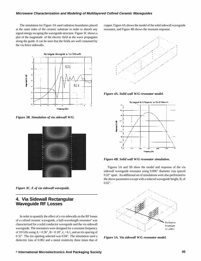
copper. Figure 4A shows the model of the solid sidewall waveguideresonator, and Figure 4B shows the resonant response.
Figure 4A. Solid wall W/G resonator model.
Figure 4B. Solid wall W/G resonator simulation.
Figures 5A and 5B show the model and response of the viasidewall waveguide resonator using 0.006” diameter vias spaced0.02” apart. An additional set of simulations were also performed tothe above parameters except with a reduced waveguide height, B, of0.02".
Figure 5A. Via sidewall W/G resonator model.
45

8 International Microelectronics And Packaging Society
The International Journal of Microcircuits and Electronic Packaging, Volume 22, Number 1, First Quarter 1999 (ISSN 1063-1674)
Intl. Journal of Microcircuits and Electronic Packaging
Figure 5B. Via sidewall W/G resonator simulation.
Table 1 summarizes the resonator simulation results, includingthe resonant frequency, the 3dB bandwidth, the loss, the unloadedQ, and the attenuation in dB/inch. Equations (1) and (2) were usedfor the calculation of unloaded Q and attenuation. From Table 1, itcan be seen that the via sidewalls add little, if any, to the RF lossesfor vias spaced less than one-tenth the guide wavelength. In thisTable, Tand = 0.002, and Rho = 3 × copper.
Table 1. Summary of waveguide resonator simulation results.
Walltype
Bdim.
FRES,GHz
B3dB,MHz
Loss@ Fc QU
Atten(dB/in)
Solid 0.18” 9.95 23.5 32.7 433 0.197Via 0.18” 9.92 23.9 28.4 432 0.197
Solid 0.02” 9.93 43.4 29.9 237 0.360Via 0.02” 9.91 43.7 30.0 233 0.364
QU=Q
L/(1-|S
21|) (1)
where QL=F
RES/B
3dB
andAttenuation = 8.686p / Q
U·L , (in dB per unit length) (2)
Figure 5C shows the loss of the waveguide for various spacingof the vias used to construct the waveguide sidewalls for an X-bandstructure. It can be readily seen that a via spacing up to 30 mils(center to center) provides similar loss to a solid sidewall waveguide(that is a spacing = 0 mils).
Figure 5C. W/G loss vs sidewall via spacing.
5. Crosstalk Between Two AdjacentWaveguides
Crosstalk between adjacent transmission lines is an importantissue for RF assemblies packaged in cofired ceramics. The abilityto obtain at least 40 dB of isolation is frequently necessary for manyapplications. For strip transmission lines, it is common practice toenclose RF signal conductors within via fences, or to place a viafence between two adjacent conductors, in order to provide the neededisolation. For even higher isolation, a double via fence can be used,as well as separating adjacent conductors electrically far apart toreduce coupling.
The HFSS model shown in Figure 6A was examined to deter-mine the crosstalk between adjacent waveguide structures using acommon via fence sidewall. This waveguide has dimensions of A =0.25", B = 0.10", a length of 0.50" and an g
r = 6.1. The via diameter
is 0.006" and via spacings of 0.02”, 0.04” and 0.06” were simulated.
Figure 6A. Common via sidewall crosstalk model.
Figure 6B. Common via fence crosstalk simulation.
Figure 7A shows a similar model except it uses two separate viafences, separated 0.02" apart, between the adjacent waveguides.Simulation results are shown in Figures 6B and 7B, for the commonvia sidewall and the separate via sidewall models, respectively. Fora 0.02” via spacing, the common via fence sidewall provides ap-proximately 50 dB isolation between adjacent waveguides while
46

The International Journal of Microcircuits and Electronic Packaging, Volume 22, Number 1, First Quarter 1999 (ISSN 1063-1674)
8 International Microelectronics And Packaging Society
Microwave Characterization and Modeling of Multilayered Cofired Ceramic Waveguides
the separate via fence sidewall provides approximately 80 dB isola-tion5.
Figure 7A. Separate via sidewall crosstalk model.
Figure 7B. Separate via fence crosstalk simulation.
6. Cofired Ceramic WaveguidePrototype
A stripline to waveguide transition was designed to facilitate test-ing of a via sidewall waveguide structure. A waveguide height of B= 0.011" was chosen since it would provide a sufficiently high lossthat could be accurately measured. An E-plane probe transition wasattempted, however this proved very unefficient in coupling to thereduced height waveguide. Instead, an end-feed transition fromstripline to waveguide was developed. In this transition, the striplineconductor is connected directly to the common center conductor oftwo stacked waveguides. Figure 8A shows the stripline to waveguidetransition.
If the stripline ground plane spacing is made equal to twice thewaveguide height, then the ground plane step discontinuity at thestripline to waveguide junction is eliminated. In order to couple thesignal into the lower waveguide, a short was placed in the topwaveguide a quarter of the guide wavelength from the stripline towaveguide junction.
Figure 8A. Stripline to W/G transition model.
The height of the top quarterwave waveguide was subsequentlyincreased to B = 0.05" in order to raise its impedance and therebyminimize its effect on the frequency response of the matched transi-tion. Figure 8B shows the response of the matched transition.
Figure 8B. Stripline to W/G transition model.
A prototype via sidewall rectangular waveguide was fabricatedin Low Temperature Cofired Ceramic (LTCC) in order to validatethe performance of the proposed waveguide structure. A rectangu-lar waveguide with dimensions A = 0.36" and B = 0.011" was builtusing 0.006" diameter vias spaced 0.02" apart for the sidewalls.Figure 9A shows the layout of the LTCC test substrate used for theprototype waveguide. The test circuit is a length of reduced heightwaveguide 2.0 inches long with two transitions to stripline at eachend.
Figure 9A. Prototype LTCC W/G w/transitions.
47
8 International Microelectronics And Packaging Society
The International Journal of Microcircuits and Electronic Packaging, Volume 22, Number 1, First Quarter 1999 (ISSN 1063-1674)
Intl. Journal of Microcircuits and Electronic Packaging
References
1. High Frequency Structure Simulator (HFSS), Hewlett PackardCompany, Westlake, California.
2. Duroid, Rogers Corp., Chandler, Arizona.3. Samuel Laio, “Microwave Devices and Circuits”, pp. 102-
119, Prentice Hall, 1990.4. G. L. Mathaei, L. Young, and E.M.T Jones, “Microwave Fil-
ters, Impedance Matching Networks, and Coupling Structures”,pg. 243, Artech House, Dedham, Massachusetts, 1985.
5. H. Uchimura, T. Takenoshita, and M. Fuji, “Development ofthe Laminated Waveguide”, IEEE MTT-S Digest, pp. 1811-1814, 1998.
About the authors
Daniel Stevens received his B.S. Degree from the Georgia Insti-tute of Technology in 1983. He joined the Westinghouse ElectricCorporation in Baltimore, Maryland in 1983, where he has workedin the area of high power solid state microwave transmitter designfor airborne radar applications. In 1996, he joined NorthropGrumman’s Electronic Sensors and Systems Division in Baltimoreas a Senior engineer and is currently involved in the active apertureT/R module development Group.
John Gipprich joined Westinghouse Electric Corporation in Bal-timore, Maryland in 1959, as a participant in the Westinghouse/JohnsHopkins Work Study Program. He received his B. S. and M. S.Degrees in Electrical Engineering from Johns Hopkins University,in 1965 and 1971, respectively. Since 1963, Mr. Gipprich has workedin the antenna and microwave areas and has been involved in micro-wave circuit and subsystems design. In 1996, he joined the NorthropGrumman Electronic Sensors and Systems Division in Baltimore.Currently, he is an Advisory engineer in the active aperture moduleengineering Department and is responsible for T/R module devel-opment and microwave multilayer cicuit designs. Mr. Gipprich is amember of IMAPS, IMAPS National Technical Committee, andIEEE/MTT-S. In 1987, he served as Chairman of the BaltimoreIEEE AP-MT Chapter.
48
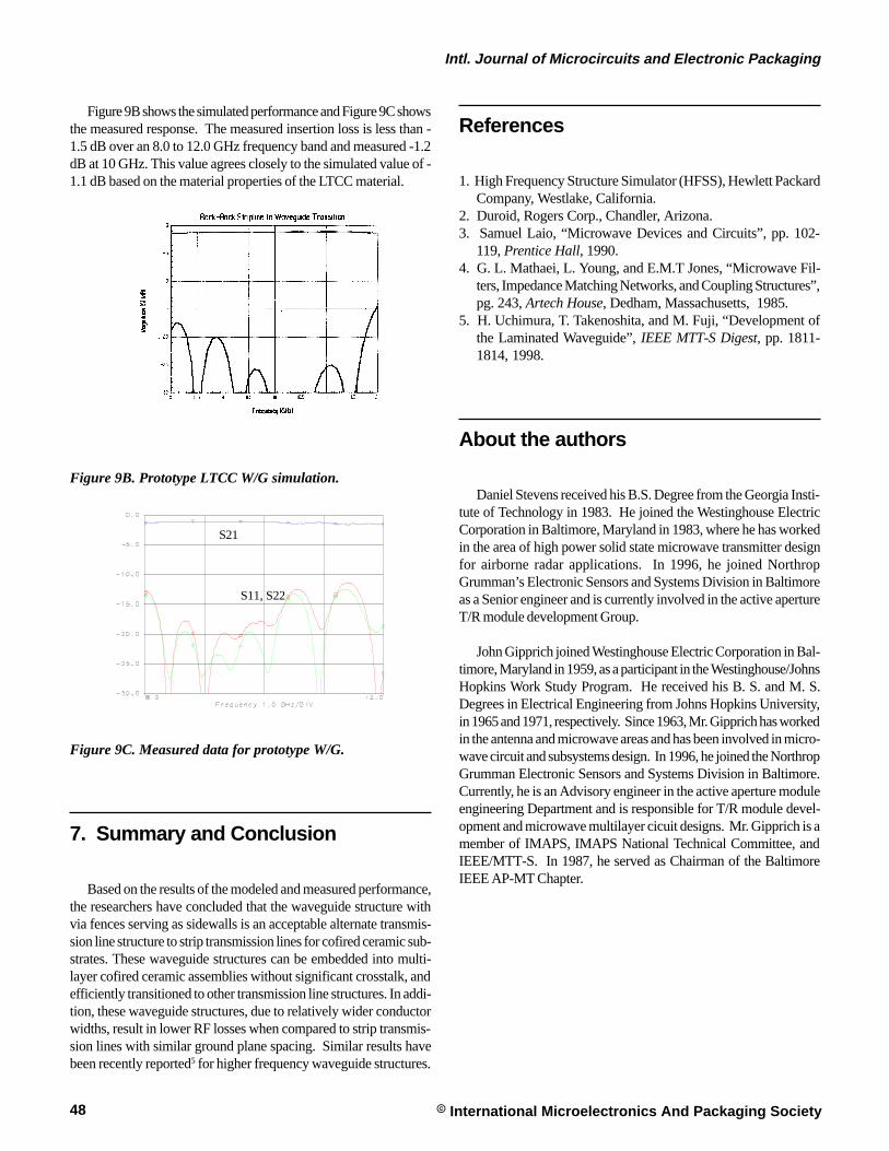
Figure 9B shows the simulated performance and Figure 9C showsthe measured response. The measured insertion loss is less than -1.5 dB over an 8.0 to 12.0 GHz frequency band and measured -1.2dB at 10 GHz. This value agrees closely to the simulated value of -1.1 dB based on the material properties of the LTCC material.
Figure 9B. Prototype LTCC W/G simulation.
S21
S11, S22
Figure 9C. Measured data for prototype W/G.
7. Summary and Conclusion
Based on the results of the modeled and measured performance,the researchers have concluded that the waveguide structure withvia fences serving as sidewalls is an acceptable alternate transmis-sion line structure to strip transmission lines for cofired ceramic sub-strates. These waveguide structures can be embedded into multi-layer cofired ceramic assemblies without significant crosstalk, andefficiently transitioned to other transmission line structures. In addi-tion, these waveguide structures, due to relatively wider conductorwidths, result in lower RF losses when compared to strip transmis-sion lines with similar ground plane spacing. Similar results havebeen recently reported5 for higher frequency waveguide structures.


![Synthesis and characterization of multilayered BaTiO3 ... 19 03.pdf · 15 Processing and Application of Ceramics 7 [1] (2013) 15–20 Synthesis and characterization of multilayered](https://img.pdfslide.net/doc/110x75/60fd07ef6c8a8a6f0e41161d/synthesis-and-characterization-of-multilayered-batio3-19-03pdf-15-processing.jpg)


![Microstructural and magnetic characterization of ion-beam ...web.nchu.edu.tw/~hfhsu/HomePage/paper/2015/Vacuum 118...barded) and argon ion-beam bombarded multilayered [Ni80Fe20-Cr]50](https://img.pdfslide.net/doc/110x75/60aa06044f1313078c37d4e6/microstructural-and-magnetic-characterization-of-ion-beam-webnchuedutwhfhsuhomepagepaper2015vacuum.jpg)